EP3396703A1 - Mécanisme de support de plaquette, appareil de dépôt chimique en phase vapeur et procédé de fabrication de plaquette épitaxiale - Google Patents
Mécanisme de support de plaquette, appareil de dépôt chimique en phase vapeur et procédé de fabrication de plaquette épitaxiale Download PDFInfo
- Publication number
- EP3396703A1 EP3396703A1 EP16878443.7A EP16878443A EP3396703A1 EP 3396703 A1 EP3396703 A1 EP 3396703A1 EP 16878443 A EP16878443 A EP 16878443A EP 3396703 A1 EP3396703 A1 EP 3396703A1
- Authority
- EP
- European Patent Office
- Prior art keywords
- wafer
- wafer supporting
- transfer
- supporting portion
- film formation
- Prior art date
- Legal status (The legal status is an assumption and is not a legal conclusion. Google has not performed a legal analysis and makes no representation as to the accuracy of the status listed.)
- Granted
Links
Images



Classifications
-
- H—ELECTRICITY
- H10—SEMICONDUCTOR DEVICES; ELECTRIC SOLID-STATE DEVICES NOT OTHERWISE PROVIDED FOR
- H10P—GENERIC PROCESSES OR APPARATUS FOR THE MANUFACTURE OR TREATMENT OF DEVICES COVERED BY CLASS H10
- H10P72/00—Handling or holding of wafers, substrates or devices during manufacture or treatment thereof
- H10P72/70—Handling or holding of wafers, substrates or devices during manufacture or treatment thereof for supporting or gripping
-
- H—ELECTRICITY
- H10—SEMICONDUCTOR DEVICES; ELECTRIC SOLID-STATE DEVICES NOT OTHERWISE PROVIDED FOR
- H10P—GENERIC PROCESSES OR APPARATUS FOR THE MANUFACTURE OR TREATMENT OF DEVICES COVERED BY CLASS H10
- H10P72/00—Handling or holding of wafers, substrates or devices during manufacture or treatment thereof
- H10P72/30—Handling or holding of wafers, substrates or devices during manufacture or treatment thereof for conveying, e.g. between different workstations
- H10P72/33—Handling or holding of wafers, substrates or devices during manufacture or treatment thereof for conveying, e.g. between different workstations into and out of processing chamber
- H10P72/3306—Horizontal transfer of a single workpiece
-
- C—CHEMISTRY; METALLURGY
- C23—COATING METALLIC MATERIAL; COATING MATERIAL WITH METALLIC MATERIAL; CHEMICAL SURFACE TREATMENT; DIFFUSION TREATMENT OF METALLIC MATERIAL; COATING BY VACUUM EVAPORATION, BY SPUTTERING, BY ION IMPLANTATION OR BY CHEMICAL VAPOUR DEPOSITION, IN GENERAL; INHIBITING CORROSION OF METALLIC MATERIAL OR INCRUSTATION IN GENERAL
- C23C—COATING METALLIC MATERIAL; COATING MATERIAL WITH METALLIC MATERIAL; SURFACE TREATMENT OF METALLIC MATERIAL BY DIFFUSION INTO THE SURFACE, BY CHEMICAL CONVERSION OR SUBSTITUTION; COATING BY VACUUM EVAPORATION, BY SPUTTERING, BY ION IMPLANTATION OR BY CHEMICAL VAPOUR DEPOSITION, IN GENERAL
- C23C16/00—Chemical coating by decomposition of gaseous compounds, without leaving reaction products of surface material in the coating, i.e. chemical vapour deposition [CVD] processes
- C23C16/44—Chemical coating by decomposition of gaseous compounds, without leaving reaction products of surface material in the coating, i.e. chemical vapour deposition [CVD] processes characterised by the method of coating
-
- C—CHEMISTRY; METALLURGY
- C23—COATING METALLIC MATERIAL; COATING MATERIAL WITH METALLIC MATERIAL; CHEMICAL SURFACE TREATMENT; DIFFUSION TREATMENT OF METALLIC MATERIAL; COATING BY VACUUM EVAPORATION, BY SPUTTERING, BY ION IMPLANTATION OR BY CHEMICAL VAPOUR DEPOSITION, IN GENERAL; INHIBITING CORROSION OF METALLIC MATERIAL OR INCRUSTATION IN GENERAL
- C23C—COATING METALLIC MATERIAL; COATING MATERIAL WITH METALLIC MATERIAL; SURFACE TREATMENT OF METALLIC MATERIAL BY DIFFUSION INTO THE SURFACE, BY CHEMICAL CONVERSION OR SUBSTITUTION; COATING BY VACUUM EVAPORATION, BY SPUTTERING, BY ION IMPLANTATION OR BY CHEMICAL VAPOUR DEPOSITION, IN GENERAL
- C23C16/00—Chemical coating by decomposition of gaseous compounds, without leaving reaction products of surface material in the coating, i.e. chemical vapour deposition [CVD] processes
- C23C16/44—Chemical coating by decomposition of gaseous compounds, without leaving reaction products of surface material in the coating, i.e. chemical vapour deposition [CVD] processes characterised by the method of coating
- C23C16/458—Chemical coating by decomposition of gaseous compounds, without leaving reaction products of surface material in the coating, i.e. chemical vapour deposition [CVD] processes characterised by the method of coating characterised by the method used for supporting substrates in the reaction chamber
-
- C—CHEMISTRY; METALLURGY
- C30—CRYSTAL GROWTH
- C30B—SINGLE-CRYSTAL GROWTH; UNIDIRECTIONAL SOLIDIFICATION OF EUTECTIC MATERIAL OR UNIDIRECTIONAL DEMIXING OF EUTECTOID MATERIAL; REFINING BY ZONE-MELTING OF MATERIAL; PRODUCTION OF A HOMOGENEOUS POLYCRYSTALLINE MATERIAL WITH DEFINED STRUCTURE; SINGLE CRYSTALS OR HOMOGENEOUS POLYCRYSTALLINE MATERIAL WITH DEFINED STRUCTURE; AFTER-TREATMENT OF SINGLE CRYSTALS OR A HOMOGENEOUS POLYCRYSTALLINE MATERIAL WITH DEFINED STRUCTURE; APPARATUS THEREFOR
- C30B25/00—Single-crystal growth by chemical reaction of reactive gases, e.g. chemical vapour-deposition growth
- C30B25/02—Epitaxial-layer growth
- C30B25/10—Heating of the reaction chamber or the substrate
- C30B25/105—Heating of the reaction chamber or the substrate by irradiation or electric discharge
-
- C—CHEMISTRY; METALLURGY
- C30—CRYSTAL GROWTH
- C30B—SINGLE-CRYSTAL GROWTH; UNIDIRECTIONAL SOLIDIFICATION OF EUTECTIC MATERIAL OR UNIDIRECTIONAL DEMIXING OF EUTECTOID MATERIAL; REFINING BY ZONE-MELTING OF MATERIAL; PRODUCTION OF A HOMOGENEOUS POLYCRYSTALLINE MATERIAL WITH DEFINED STRUCTURE; SINGLE CRYSTALS OR HOMOGENEOUS POLYCRYSTALLINE MATERIAL WITH DEFINED STRUCTURE; AFTER-TREATMENT OF SINGLE CRYSTALS OR A HOMOGENEOUS POLYCRYSTALLINE MATERIAL WITH DEFINED STRUCTURE; APPARATUS THEREFOR
- C30B25/00—Single-crystal growth by chemical reaction of reactive gases, e.g. chemical vapour-deposition growth
- C30B25/02—Epitaxial-layer growth
- C30B25/12—Substrate holders or susceptors
-
- C—CHEMISTRY; METALLURGY
- C30—CRYSTAL GROWTH
- C30B—SINGLE-CRYSTAL GROWTH; UNIDIRECTIONAL SOLIDIFICATION OF EUTECTIC MATERIAL OR UNIDIRECTIONAL DEMIXING OF EUTECTOID MATERIAL; REFINING BY ZONE-MELTING OF MATERIAL; PRODUCTION OF A HOMOGENEOUS POLYCRYSTALLINE MATERIAL WITH DEFINED STRUCTURE; SINGLE CRYSTALS OR HOMOGENEOUS POLYCRYSTALLINE MATERIAL WITH DEFINED STRUCTURE; AFTER-TREATMENT OF SINGLE CRYSTALS OR A HOMOGENEOUS POLYCRYSTALLINE MATERIAL WITH DEFINED STRUCTURE; APPARATUS THEREFOR
- C30B25/00—Single-crystal growth by chemical reaction of reactive gases, e.g. chemical vapour-deposition growth
- C30B25/02—Epitaxial-layer growth
- C30B25/14—Feed and outlet means for the gases; Modifying the flow of the reactive gases
-
- H—ELECTRICITY
- H10—SEMICONDUCTOR DEVICES; ELECTRIC SOLID-STATE DEVICES NOT OTHERWISE PROVIDED FOR
- H10P—GENERIC PROCESSES OR APPARATUS FOR THE MANUFACTURE OR TREATMENT OF DEVICES COVERED BY CLASS H10
- H10P14/00—Formation of materials, e.g. in the shape of layers or pillars
- H10P14/20—Formation of materials, e.g. in the shape of layers or pillars of semiconductor materials
-
- H—ELECTRICITY
- H10—SEMICONDUCTOR DEVICES; ELECTRIC SOLID-STATE DEVICES NOT OTHERWISE PROVIDED FOR
- H10P—GENERIC PROCESSES OR APPARATUS FOR THE MANUFACTURE OR TREATMENT OF DEVICES COVERED BY CLASS H10
- H10P14/00—Formation of materials, e.g. in the shape of layers or pillars
- H10P14/60—Formation of materials, e.g. in the shape of layers or pillars of insulating materials
-
- H—ELECTRICITY
- H10—SEMICONDUCTOR DEVICES; ELECTRIC SOLID-STATE DEVICES NOT OTHERWISE PROVIDED FOR
- H10P—GENERIC PROCESSES OR APPARATUS FOR THE MANUFACTURE OR TREATMENT OF DEVICES COVERED BY CLASS H10
- H10P72/00—Handling or holding of wafers, substrates or devices during manufacture or treatment thereof
- H10P72/10—Handling or holding of wafers, substrates or devices during manufacture or treatment thereof using carriers specially adapted therefor, e.g. front opening unified pods [FOUP]
- H10P72/18—Handling or holding of wafers, substrates or devices during manufacture or treatment thereof using carriers specially adapted therefor, e.g. front opening unified pods [FOUP] characterised by being specially adapted for supporting a single substrate or by comprising a stack of such individual supports
-
- H—ELECTRICITY
- H10—SEMICONDUCTOR DEVICES; ELECTRIC SOLID-STATE DEVICES NOT OTHERWISE PROVIDED FOR
- H10P—GENERIC PROCESSES OR APPARATUS FOR THE MANUFACTURE OR TREATMENT OF DEVICES COVERED BY CLASS H10
- H10P72/00—Handling or holding of wafers, substrates or devices during manufacture or treatment thereof
- H10P72/70—Handling or holding of wafers, substrates or devices during manufacture or treatment thereof for supporting or gripping
- H10P72/76—Handling or holding of wafers, substrates or devices during manufacture or treatment thereof for supporting or gripping using mechanical means, e.g. clamps or pinches
- H10P72/7604—Handling or holding of wafers, substrates or devices during manufacture or treatment thereof for supporting or gripping using mechanical means, e.g. clamps or pinches the wafers being placed on a susceptor, stage or support
- H10P72/7612—Handling or holding of wafers, substrates or devices during manufacture or treatment thereof for supporting or gripping using mechanical means, e.g. clamps or pinches the wafers being placed on a susceptor, stage or support characterised by lifting arrangements, e.g. lift pins
-
- H—ELECTRICITY
- H10—SEMICONDUCTOR DEVICES; ELECTRIC SOLID-STATE DEVICES NOT OTHERWISE PROVIDED FOR
- H10P—GENERIC PROCESSES OR APPARATUS FOR THE MANUFACTURE OR TREATMENT OF DEVICES COVERED BY CLASS H10
- H10P72/00—Handling or holding of wafers, substrates or devices during manufacture or treatment thereof
- H10P72/70—Handling or holding of wafers, substrates or devices during manufacture or treatment thereof for supporting or gripping
- H10P72/76—Handling or holding of wafers, substrates or devices during manufacture or treatment thereof for supporting or gripping using mechanical means, e.g. clamps or pinches
- H10P72/7604—Handling or holding of wafers, substrates or devices during manufacture or treatment thereof for supporting or gripping using mechanical means, e.g. clamps or pinches the wafers being placed on a susceptor, stage or support
- H10P72/7618—Handling or holding of wafers, substrates or devices during manufacture or treatment thereof for supporting or gripping using mechanical means, e.g. clamps or pinches the wafers being placed on a susceptor, stage or support characterised by a movable susceptor, stage or support, others than those only rotating on their own vertical axis, e.g. susceptors on a rotating carrousel
Definitions
- the present invention relates to a wafer supporting mechanism, a chemical vapor deposition apparatus, and a method of manufacturing an epitaxial wafer.
- a chemical vapor deposition (CVD) method has been known as methods for forming a thin film layer on a substrate.
- CVD chemical vapor deposition
- a SiC epitaxial layer is formed on a SiC wafer by using a chemical vapor deposition apparatus to produce a SiC epitaxial wafer.
- wafer before epitaxial layer formation
- epitaxial wafer a wafer after epitaxial layer formation
- Patent Document 1 describes that a substrate is transferred while being installed on a susceptor (wafer supporting table) and film formation is performed as it is in order to suppress the shape change of the wafer due to high temperature transfer.
- the shape change of the wafer during high temperature transfer becomes more prominent as the temperature difference between the film formation space and the external environment increases.
- the temperature in the film formation space may be increased up to 1,500°C or higher. Even during the high temperature transfer, the temperature of the film formation space is as high as 700 to 1,200°C.
- Patent Document 2 describes that in a CVD apparatus for manufacturing a SiC epitaxial wafer requiring high temperature growth, a susceptor on which a wafer is carried is transferred using a transfer robot.
- Patent Document 3 describes that when the entire wafer surface is placed on a susceptor, the wafer warps concavely toward the wafer front surface side due to heating from the back surface. In addition, as means for suppressing problems caused by such warpage, it is described that the wafer is supported only at the peripheral edge portion of the wafer.
- the present invention takes the above problems into consideration, and has an object of providing a wafer supporting mechanism which is capable of suppressing breakage of a wafer caused by the thermal stress applied to the wafer, a chemical vapor deposition apparatus, and a method of manufacturing an epitaxial wafer.
- the inventors of the present invention have found that by changing the position for supporting the wafer at the time of high temperature transfer and the position for supporting the wafer at the time of film formation process, breakage of the wafer due to the thermal stress applied to the wafer can be suppressed.
- the present invention provides the following procedures in order to solve the above problems.
- the chemical vapor deposition apparatus and the method of manufacturing an epitaxial wafer according to one aspect of the present invention it is possible to suppress the breakage of the wafer due to the thermal stress applied to the wafer.
- FIG. 1 is a schematic cross-sectional view of a chemical vapor deposition apparatus according to one aspect of the present invention.
- a chemical vapor deposition apparatus 100 shown in FIG. 1 has a furnace body 30 for forming a film formation space R and a preparation chamber 40 for forming a transfer space P.
- the furnace body 30 and the preparation chamber 40 are partitioned by a shutter 31.
- An installation part 20 for installing a wafer supporting mechanism 10 on which a wafer W is placed is provided below the furnace body 30.
- the installation part 20 is supported by a supporting column 21, and the supporting column 21 is rotatable.
- a gas supply pipe and a heater and the like (not shown) are installed.
- the gas supply pipe supplies a source gas, a carrier gas, an etching gas, and the like to the film formation space R, and the heater heats the inside of the film formation space R.
- the film formation surface side of the wafer W may be referred to as being above, and the side opposite to the film formation surface may be referred to as being below.
- the wafer W is placed on the wafer supporting mechanism 10.
- the wafer supporting mechanism 10 on which the wafer W is placed is transferred to the furnace body 30 by an arm 41 after opening the shutter 31 which is provided between the preparation chamber 40 and the furnace body 30.
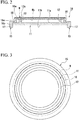
- FIG. 2 is a schematic cross-sectional view of a wafer supporting mechanism according to one aspect of the present invention.
- FIG. 3 is a schematic plan view of the wafer supporting mechanism according to the present embodiment.
- the wafer W is shown at the same time.
- the wafer supporting mechanism 10 shown in FIG. 2 is separated into and configured by a wafer supporting table 11 and a movable part 15.
- the wafer supporting table 11 has a wafer supporting portion for transfer 12 that stands up from a first surface 11a facing a back surface Wb of the placed wafer W.
- the wafer supporting portion for transfer 12 is provided, in plan view, further inside than the outer periphery of the wafer W to be placed. More specifically, the outer periphery of the wafer supporting portion for transfer 12 is present, preferably 2 mm or more, and more preferably 6 mm or more, toward the inner side than the outer periphery of the wafer W.
- the diameter of a circle formed by the wafer supporting portion for transfer 12 is preferably 97% or less, more preferably 92% or less, and still more preferably 80% or less of the diameter of the wafer W to be placed.
- a suitable width or position can be selected depending on the size of the wafer and the structure of the movable part and the wafer supporting portion for film formation that are supported by the wafer supporting table.
- the "outer periphery of the wafer supporting portion for transfer” indicates the outer peripheral edge of the supporting portion.
- the diameter of a circle formed by the wafer supporting portion for transfer indicates the diameter of a circle serving as the outer periphery of the wafer supporting portion for transfer.
- the thermal stress applied to the wafer W when the wafer W is transferred at a high temperature reaches the maximum at a portion supporting the wafer W.
- the wafer supporting mechanism 10 has a larger heat capacity than that of the wafer W, and is more difficult to be heated than the wafer when transferred at a high temperature. Accordingly, during high temperature transfer, the wafer supporting mechanism 10 is in a state of having a lower temperature than that of the wafer W. Therefore, the heat of the wafer W escapes from the portion which is in contact with the wafer supporting portion for transfer 12 to the supporting portion having a relatively low temperature. As a result, the wafer temperature at the portion which is in contact with the wafer supporting portion for transfer 12 is lowered, and a temperature distribution is formed within the wafer W. It is due to this temperature distribution that the thermal stress applied to the wafer W reaches the maximum at the portion where the wafer W is supported.
- the breaking strength of the outer peripheral portion is smaller than the inner breaking strength. Therefore, when a stress is applied to the outer peripheral portion rather than to the inner peripheral portion, the wafer easily cracks. In order to suppress the cracking of the wafer, it is important to reduce the stress to the outer peripheral portion. By setting the position of the wafer supporting portion for transfer 12, that supports the wafer W during transfer, further inside than the outer periphery of the wafer W to be placed, it is possible to reduce the stress to the outer peripheral portion and to suppress the cracking of the wafer.
- the diameter of the circle formed by the wafer supporting portion for transfer 12 is preferably 30% or more, and more preferably 50% or more of the diameter of the wafer W to be placed.
- the wafer supporting portion for transfer refers to a portion that supports the wafer in a state immediately before the wafer is set to the position used during epitaxial growth.
- the wafer supporting portion for transfer supports the wafer inside the outer peripheral edge of the wafer in order to suppress cracking of the wafer when the temperature of the wafer and the supporting portion for transfer changes.
- a supporting portion for ultimately moving the wafer to the position which is used at the time of epitaxial growth is the wafer supporting portion for transfer according to the present embodiment.
- the movable part 15 is positioned on the outer periphery of the wafer supporting table 11.
- the movable part 15 shown in FIG. 2 includes an extension portion 15a extending along the wafer supporting table from the outer peripheral edge toward the center of the wafer supporting table 11, and a suspension portion 15b suspended downward from the extension portion 15a.
- the movable part 15 is supported such that the extension portion 15a is suspended on the wafer supporting table 11.
- a part of the suspension portion 15b protrudes from the back surface (second surface) 11b of the wafer supporting table 11 and functions as a push-up portion 17.
- a wafer supporting portion for film formation 16 that stands toward the wafer W is provided.
- the wafer supporting portion for film formation 16 is located further on the outer peripheral side of the wafer W than the wafer supporting portion for transfer 12.
- An upper surface 16a of the wafer supporting portion for film formation 16 on the wafer W side is present below an upper surface 12a of the wafer supporting portion for transfer 12 on the wafer W side in a state where the movable part 15 is suspended from the wafer supporting table 11.
- the movable part 15 can be relatively moved with respect to the wafer supporting table 11 in the standing direction of the wafer supporting portion for transfer 12.
- the wafer supporting portion for film formation 16 moves upward together with the movable part 15, so that the upper surface 16a of the wafer supporting portion for film formation 16 and the back surface Wb of the wafer W come into contact.
- the wafer supporting portion for film formation 16 supports the wafer W. That is, the position for supporting the wafer W changes from the wafer supporting portion for transfer 12 to the wafer supporting portion for film formation 16.
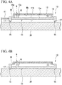
- FIG. 4A is a schematic cross-sectional view of a wafer supporting mechanism for supporting a wafer at the time of transfer
- FIG. 4B is a schematic cross-sectional view of a wafer supporting mechanism for supporting the wafer at the time of film formation.
- the wafer supporting mechanism 10 is supported and transferred by the arm 41.
- the movable part 15 In a transferred state, the movable part 15 is in a state of being suspended from the wafer supporting table 11. Therefore, as in FIG. 2 , a part of the movable part 15 protrudes from the second surface 11b of the wafer supporting table 11.
- the protruding portion is the push-up portion 17.
- the wafer W In a transferred state, the wafer W is supported by the wafer supporting portion for transfer 12. Therefore, even when the film formation space R in FIG. 1 is at a high temperature, the generated thermal stress per se can be reduced, and the moment generated by the thermal stress can also be reduced. As a result, damage to the wafer W can be prevented.
- the wafer supporting mechanism 10 is installed on the installation part 20 of the furnace body 30 shown in FIG. 1 . Therefore, the push-up portion 17 protruding from the second surface 11b of the wafer supporting table 11 is pushed up by the installation part 20. Accordingly, the entire movable part 15 is pushed upward. As a result, the portion for supporting the wafer W changes from the wafer supporting portion for transfer 12 to the wafer supporting portion for film formation 16.
- the wafer warps into a concave shape with respect to the installation part 20.
- the position of the outer peripheral portion of the warped wafer may be located above the upper surface of a wafer side surface supporting portion which is provided on the outer peripheral side of the wafer in order to suppress positional deviation of the wafer in some cases. In this case, there is nothing to suppress the positional deviation of the wafer from the side surface, and the possibility of occurrence of positional deviation increases.
- the wafer deviates from a predetermined position during epitaxial growth, the targeted film formation quality cannot be achieved.
- the central portion of the wafer merely shifts downward even if the wafer warps, and the position of the outer peripheral portion of the wafer does not change from the position supported by the wafer supporting portion. That is, the positional relationship between the outer peripheral portion of the wafer and the wafer side surface supporting portion does not change, and positional deviation of the wafer hardly occurs.
- the thermal stress is alleviated. Therefore, even if the wafer W is supported at the outer peripheral edge portion of the wafer W, the wafer W will not be damaged by the thermal stress.
- the position of the wafer supporting portion for film formation 16 is further on the outer peripheral side of the wafer W to be placed than the wafer supporting portion for transfer 12, and at least a part of the wafer supporting portion for film formation 16 is in contact with the outer peripheral edge of the wafer W.
- a wafer side surface supporting portion for supporting the side surface of the wafer W as described above in the wafer supporting mechanism 10.
- the chemical vapor deposition apparatus supports the wafer W at the time of transfer by the wafer supporting portion for transfer 12 that is provided further inside than the outer periphery of the wafer W to be placed, so that it is possible to avoid breakage of the wafer due to the thermal stress. Especially when using a wafer with a large diameter, or when the temperature before transfer and the temperature after transfer are greatly different, the effect is remarkable. Further, at the time of film formation, since the wafer W is supported by the wafer supporting portion for film formation 16 that is arranged further on the outer peripheral side of the wafer W to be placed than the wafer supporting portion for transfer 12, it is possible to enhance the quality of the obtained epitaxial wafer.
- the chemical vapor deposition apparatus can be used for chemical vapor deposition in which a wafer is inserted one by one, and also for chemical vapor deposition in which a plurality of wafers are simultaneously inserted, into a reaction space in an epitaxial reaction furnace.
- the effect is particularly great in the case of an apparatus that transfers wafers one by one because the number of times of transfer is large.
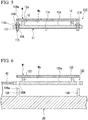
- FIG. 5 is a schematic cross-sectional view of a modified example of a wafer supporting mechanism according to one aspect of the present invention.
- a movable part 115 having a wafer supporting portion for film formation 116 is inserted in a through hole 11A provided in the wafer supporting table 11.
- the movable part 115 is suspended from the wafer supporting table 11 by a protrusion portion 116b that stands up in the in-plane direction of the wafer supporting table 11 at the time of transfer.
- the wafer supporting mechanism 110 is installed in an installation part.
- a push-up portion 117 of the movable part 115 which is protruding from the second surface 11b of the wafer supporting table 11, is pushed up by the installation part.
- the entire movable part 115 is pushed up, and the wafer supporting portion for film formation 116 also moves upward.
- an upper surface 116a of the wafer supporting portion for film formation 116 comes into contact with the wafer W, and the portion for supporting the wafer W changes from the wafer supporting portion for transfer 12 to the wafer supporting portion for film formation 116.
- the wafer supporting portion for transfer 12 of the wafer supporting mechanism 110 shown in FIG. 5 is provided further inside than the outer peripheral edge of the wafer to be placed, cracking of the wafer W due to thermal stress can be avoided.
- the wafer supporting portion for film formation 116 in the wafer supporting mechanism 110 is disposed further on the outer peripheral side of the wafer W to be placed than the wafer supporting portion for transfer 12, it is possible to enhance the quality of the obtained epitaxial wafer.
- FIG. 6 is a schematic cross-sectional view of a wafer supporting mechanism according to another embodiment of the present invention, and is a schematic cross-sectional view showing a state immediately before a susceptor is installed in an installation part.
- a wafer supporting table 120 shown in FIG. 6 has a wafer supporting portion for transfer 122 that protrudes from a first surface 120a opposing the back surface Wb of the wafer W and is provided further inside than the outer peripheral edge of the wafer to be placed, and a through hole 120A is provided further on the outer peripheral side of the wafer W to be placed than the wafer supporting portion for transfer 122.
- a wafer supporting portion for film formation 126 that stands up from a surface of the installation part 20 on the film formation direction side is provided.
- the position of the wafer supporting portion for film formation 126 corresponds to the position of the through hole 120A of the wafer supporting table 120.
- the wafer supporting table 120 shown in FIG. 6 is transferred by the arm 41.
- the wafer W is supported by the wafer supporting portion for transfer 122 of the wafer supporting table 120. Since the wafer supporting portion for transfer 122 is provided further inside than the outer peripheral edge of the wafer to be placed, cracking of the wafer W due to thermal stress can be avoided.
- the wafer supporting portion for film formation 126 When installing the wafer supporting table 120 in the installation part 20, the wafer supporting portion for film formation 126 is inserted into the through hole 120A of the wafer supporting table 120.
- the inserted wafer supporting portion for film formation 126 penetrates the through hole 120A and supports the wafer W.
- the height of the wafer supporting portion for film formation 126 is larger than the combined thickness of the wafer supporting portion for transfer 122 and the through hole 120A.
- an upper surface 126a of the wafer supporting portion for film formation 126 provided in the installation part 20 comes into contact with the wafer W, and the portion for supporting the wafer W changes from the wafer supporting portion for transfer 122 to the wafer supporting portion for film formation 126.
- the wafer supporting portion for film formation 126 is disposed further on the outer peripheral side of the wafer W to be placed than the wafer supporting portion for transfer 122, it is possible to enhance the quality of the obtained epitaxial wafer.
- a configuration may be adopted in which the wafer supporting portion for film formation is moved in the vertical direction by electric drive.
- the temperature in the furnace body 30 rises up to almost 1,500°C, it is required to shield the drive circuit and the like from the heat.
- the shape of the wafer supporting mechanism as seen in a plan view can also be variously changed.
- both the wafer supporting portion for transfer 12 and the wafer supporting portion for film formation 16 are formed into an annular shape.
- the wafer supporting portion for transfer 12 and the wafer supporting portion for film formation 16 do not necessarily need to be annular, and wafer supporting portions for transfer 132 may be scattered about as shown in FIG. 7 .
- the wafer supporting portions for transfer 132 may be randomly scattered about, it is preferable that they are present on a concentric circle from the viewpoint of stability.
- the "diameter of a circle formed by the wafer supporting portion for transfer" means the diameter of the largest circle that can be drawn by connecting the scattered wafer supporting portions for transfer 132.
- the wafer supporting portion for film formation 16 may also have a shape in which a part of a circular ring is cut out.
- the installation part 20 is also not particularly limited as long as it can support the wafer supporting mechanism 10.
- it can adopt various shapes such as a disc shape, an annular shape and the like.
- the method of manufacturing an epitaxial wafer according to the present embodiment is a method of manufacturing an epitaxial wafer in which a wafer is transferred from a transfer space to a film formation space higher in temperature than the transfer space, and a layer is formed on the wafer in the film formation space.
- the method of manufacturing an epitaxial wafer according to the present embodiment includes: a placing step of placing a wafer on a wafer supporting portion for transfer of a wafer supporting table; a transfer step of transferring the wafer together with the wafer supporting table from the transfer space to the film formation space; and a film formation step of installing the transferred wafer supporting table in the film formation space and forming a layer on the wafer.
- a method of manufacturing an epitaxial wafer will be specifically described with reference to the chemical vapor deposition apparatus shown in FIG. 1 and the wafer supporting mechanism shown in FIG. 2 as examples.
- the wafer W is placed on the wafer supporting portion for transfer 12 of the wafer supporting table 11.
- the wafer supporting portion for transfer 12 is set to be located further inside than the outer periphery of the wafer W to be placed thereon. It is preferable that the center of the circle formed by the wafer supporting portion for transfer 12 and the center of the wafer W to be placed are made to coincide. By making these centers coincide with each other, it is easy for the rotation axis of the supporting column 21 for supporting the installation part 20 to coincide with the center of the wafer W, and the obtained epitaxial wafer can be made homogeneous. Further, the stability of the wafer W at the time of transfer can also be enhanced.
- the wafer supporting mechanism 10 on which the wafer W is placed is introduced into a transfer space P and installed on an arm 41 for transfer.
- Installation of the arm 41 and the wafer supporting mechanism 10 is not particularly limited. For example, it is possible to provide a screw hole in the wafer supporting mechanism 10, insert the arm 41 into the screw hole, and install the wafer supporting mechanism 10 on the arm 41.
- the temperature in the transfer space P is preferably about a temperature at which a person can perform an operation from the viewpoint of workability, and for example, it is preferably room temperature.
- the shutter 31 that partitions the furnace body 30 from the preparation chamber 40 is opened, and the wafer W is transferred together with the wafer supporting mechanism 10 from the transfer space P to the film formation space R.
- the transfer space P is subjected to a decompression treatment or the like as necessary.
- the temperature of the film formation space R is higher than that of the transfer space P. More specifically, for example, when fabricating a SiC epitaxial wafer, the temperature at which epitaxial growth is performed is 1,500°C or higher. Therefore, it is preferable that the temperature of the film formation space R is 700°C or more even at the time of transfer.
- the thermal stress applied to the wafer W reaches the maximum at a portion supporting the wafer W.
- the wafer supporting portion for transfer 12 is placed so as to be located further inside than the outer periphery of the wafer W to be placed in the placing step. Therefore, it is possible to avoid the application of an excessive moment to the wafer W, and cracking of the wafer W can be avoided.
- the effect of suppressing cracking of the wafer W is effective if it is during transfer between environments having a temperature difference. Above all, this effect is particularly remarkable when an epitaxial wafer is produced which requires an extremely high temperature of about 1,500°C for epitaxial growth such as SiC epitaxial wafers and the like.
- the temperature of the film formation space R at the time of transfer is preferably 700°C or more.
- the temperature difference between the transfer space P and the film formation space R is 650°C or more.
- the wafer supporting mechanism 10 transferred into the film formation space R is installed in the installation part 20 provided in the furnace body 30.
- the position for supporting the wafer is switched from the wafer supporting portion for transfer 12 to the wafer supporting portion for film formation 16.
- the switching direction is not particularly limited, but it can be realized by using, for example, the wafer supporting mechanism or the like shown in FIGS. 2 , 5, and 6 .
- the wafer supporting portion for film formation 16 is located further on the outer peripheral side of the wafer W than the wafer supporting portion for transfer 12.
- an epitaxial layer is formed on the wafer W.
- the portion for supporting the wafer W is changed from the wafer supporting portion for transfer 12 that supports the wafer W at the time of transfer to the outer peripheral side of the wafer W.
- a known chemical vapor deposition (CVD) method or the like can be used as a method of forming an epitaxial layer.
- CVD chemical vapor deposition
- heating is performed while introducing a source gas, a dopant gas, an etching gas, a carrier gas and the like into the furnace body 30.
- the source gas decomposed by heating reacts on the surface of the SiC wafer, whereby the epitaxial layer grows and the SiC epitaxial wafer is obtained.
- the wafer supporting mechanism and the chemical vapor deposition apparatus according to the present embodiment can also be applied to devices other than the SiC epitaxial growth apparatus, it is particularly effective in, and preferably used for, SiC epitaxial growth where the epitaxial growth temperature is high.
- the method of manufacturing a SiC epitaxial wafer according to the present embodiment it is possible to avoid cracking of the wafer at the time of transfer.
- the epitaxial layer grown at the time of film formation can be made homogeneous.
- FIG. 8 is a cross-sectional view of a wafer supporting table used for simulation.
- a width w of a wafer supporting portion 141 of a wafer supporting table 140 was 2 mm.
- the temperature below the wafer supporting table 140 was set to 1,000°C, and the temperature at the side thereof was set to 900°C.
- the temperature below the wafer supporting table corresponds to a heater for heating the susceptor in the chemical vapor deposition apparatus, and the temperature at the side thereof corresponds to radiation heating from the side surface of the furnace body.
- simulation result becomes bilaterally symmetric about the center of the wafer, simulation was performed from the center to one end of the wafer in order to suppress the calculation load.
- the stress applied to the wafer W was simulated while changing the distance d from the outer peripheral edge of the wafer W to the outer peripheral edge of the wafer supporting portion 141.
- the stress when a wafer having a diameter of 100 mm was placed on the wafer supporting table was determined.
- a portion supported by the wafer supporting portion was set at a position of 48 to 50 mm from the center of the wafer. That is, the outer periphery of the wafer supporting portion is provided at a position of 0 mm from the outer periphery of the placed wafer.
- the radius (50 mm) of the circle formed by the wafer supporting portion is 100% of the radius (50 mm) of the wafer to be placed.
- the stress when a wafer having a diameter of 100 mm was placed on the wafer supporting table was determined.
- a portion supported by the wafer supporting portion was set at a position of 46 to 48 mm from the center of the wafer. That is, the outer periphery of the wafer supporting portion is provided at a position of 2 mm from the outer periphery of the placed wafer.
- the radius (48 mm) of the circle formed by the wafer supporting portion is 96% of the radius (50 mm) of the wafer to be placed.
- the stress when a wafer having a diameter of 100 mm was placed on the wafer supporting table was determined.
- a portion supported by the wafer supporting portion was set at a position of 44 to 46 mm from the center of the wafer. That is, the outer periphery of the wafer supporting portion is provided at a position of 4 mm from the outer periphery of the placed wafer.
- the radius (46 mm) of the circle formed by the wafer supporting portion is 92% of the radius (50 mm) of the wafer to be placed.
- FIGS. 9 to 11 are diagrams showing simulation results under the conditions of Comparative Example 1-1 and Examples 1-1 and 1-2.
- FIG. 9 corresponds to Comparative Example 1-1
- FIG. 10 corresponds to Example 1-1
- FIG. 11 corresponds to Example 1-2.
- the temperature of the wafer W is the lowest at a portion that is in contact with the wafer supporting portion. This is because the thermal conductivity differs between a portion that is in contact with the wafer supporting portion and a portion that is not in contact therewith.
- Example 1-1 Comparative Example 1-1 ( FIG. 9 ) compared to those in Example 1-1 and Example 1-2 ( FIG. 10 , FIG. 11 ).
- the lowest temperature portion is present in the middle of the diameter direction of the wafer as shown in FIG. 10 and FIG. 11 , since the ambient temperature also changes gently, the stress is dispersed in the radial direction of the wafer.
- FIG. 9 when the lowest temperature portion is present at the edge portion of the wafer, the stress cannot be dispersed and the maximum stress increases.
- the breaking strength of the outer peripheral portion is smaller than the breaking strength of the inner portion. Therefore, the wafer cracks more easily when a stress is applied to the outer peripheral portion rather than to the inner peripheral portion.
- it is important to reduce the stress to the outer peripheral portion By setting the position of the wafer supporting portion further inside than the outer periphery of the wafer to be placed, it is possible to reduce the stress to the outer peripheral portion and to suppress the cracking of the wafer.
- the stress when a wafer having a diameter of 150 mm was placed on the wafer supporting table was determined.
- a portion supported by the wafer supporting portion was set at a position of 73 to 75 mm from the center of the wafer. That is, the outer periphery of the wafer supporting portion is provided at a position of 0 mm from the outer periphery of the placed wafer.
- the radius (75 mm) of the circle formed by the wafer supporting portion is 100% of the radius (75 mm) of the wafer to be placed.
- the stress when a wafer having a diameter of 150 mm was placed on the wafer supporting table was determined.
- a portion supported by the wafer supporting portion was set at a position of 71 to 73 mm from the center of the wafer. That is, the outer periphery of the wafer supporting portion is provided at a position of 2 mm from the outer periphery of the placed wafer.
- the radius (73 mm) of the circle formed by the wafer supporting portion is 97% of the radius (75 mm) of the wafer to be placed.
- the stress when a 6-inch wafer (having a diameter of 152.4 mm) was placed on the wafer supporting table was determined.
- a portion supported by the wafer supporting portion was set at a position of 69 to 71 mm from the center of the wafer. That is, the outer periphery of the wafer supporting portion is provided at a position of 4 mm from the outer periphery of the placed wafer.
- the radius (71 mm) of the circle formed by the wafer supporting portion is 95% of the radius (75 mm) of the wafer to be placed.
- FIGS. 12 to 14 are diagrams showing simulation results under the conditions of Comparative Example 2-1 and Examples 2-1 and 2-2.
- FIG. 12 corresponds to Comparative Example 2-1
- FIG. 13 corresponds to Example 2-1
- FIG. 14 corresponds to Example 2-2.
- the temperature of the wafer W is the lowest at a portion that is in contact with the wafer supporting portion.
- the maximum stress is larger in Comparative Example 2-1 ( FIG. 12 ) compared to those in Example 2-1 and Example 2-2 ( FIG. 13, FIG. 14 ). It is considered that this is because the lowest temperature portion is present at the edge portion of the wafer, and thus the stress cannot be dispersed. Further, when the main stresses at the edge portions of the wafers are compared, they are 180 MPa in Comparative Example 2-1 ( FIG. 12 ), 150 MPa in Example 2-1 ( FIG. 13 ) and 110 MPa in Example 2-2 ( FIG. 14 ). In the wafer, the breaking strength of the outer peripheral portion is smaller than the breaking strength of the inner portion. Therefore, the wafer cracks more easily when a stress is applied to the outer peripheral portion rather than to the inner peripheral portion.
- 100 Chemical vapor deposition apparatus; 10, 110: Wafer supporting mechanism; 11, 120, 140: Wafer supporting table; 11a, 120a: First surface; 11b: Second surface; 11A, 120A: Through hole; 12, 122, 132: Wafer supporting portion for transfer; 12a, 16a, 116a, 126a: Upper surface; 15, 115: Movable part; 15a: Extension portion; 15b: Suspension portion; 16, 116, 126: Wafer supporting portion for film formation; 115b: Protrusion portion; 17, 117: Push-up portion; 20: Installation part; 21: Supporting column; 30: Furnace body; 31: Shutter; 40: Preparation chamber; 41: Arm; 141: Wafer supporting portion; P: Transfer space; R: Film formation space; W: Wafer; Wb: Back surface
Landscapes
- Chemical & Material Sciences (AREA)
- Chemical Kinetics & Catalysis (AREA)
- General Chemical & Material Sciences (AREA)
- Engineering & Computer Science (AREA)
- Materials Engineering (AREA)
- Metallurgy (AREA)
- Organic Chemistry (AREA)
- Crystallography & Structural Chemistry (AREA)
- Mechanical Engineering (AREA)
- Container, Conveyance, Adherence, Positioning, Of Wafer (AREA)
- Chemical Vapour Deposition (AREA)
- Crystals, And After-Treatments Of Crystals (AREA)
Applications Claiming Priority (2)
| Application Number | Priority Date | Filing Date | Title |
|---|---|---|---|
| JP2015249024A JP6539929B2 (ja) | 2015-12-21 | 2015-12-21 | ウェハ支持機構、化学気相成長装置およびエピタキシャルウェハの製造方法 |
| PCT/JP2016/086898 WO2017110552A1 (fr) | 2015-12-21 | 2016-12-12 | Mécanisme de support de plaquette, appareil de dépôt chimique en phase vapeur et procédé de fabrication de plaquette épitaxiale |
Publications (3)
| Publication Number | Publication Date |
|---|---|
| EP3396703A1 true EP3396703A1 (fr) | 2018-10-31 |
| EP3396703A4 EP3396703A4 (fr) | 2019-08-21 |
| EP3396703B1 EP3396703B1 (fr) | 2023-06-07 |
Family
ID=59090209
Family Applications (1)
| Application Number | Title | Priority Date | Filing Date |
|---|---|---|---|
| EP16878443.7A Active EP3396703B1 (fr) | 2015-12-21 | 2016-12-12 | Mécanisme de support de plaquette, appareil de dépôt chimique en phase vapeur et procédé de fabrication de plaquette épitaxiale |
Country Status (6)
| Country | Link |
|---|---|
| US (1) | US11427929B2 (fr) |
| EP (1) | EP3396703B1 (fr) |
| JP (1) | JP6539929B2 (fr) |
| KR (1) | KR102143287B1 (fr) |
| CN (1) | CN108475635B (fr) |
| WO (1) | WO2017110552A1 (fr) |
Families Citing this family (10)
| Publication number | Priority date | Publication date | Assignee | Title |
|---|---|---|---|---|
| CN109423626B (zh) * | 2017-08-30 | 2021-07-09 | 胜高股份有限公司 | 成膜装置、成膜用托盘、成膜方法、成膜用托盘的制造方法 |
| JP7322365B2 (ja) * | 2018-09-06 | 2023-08-08 | 株式会社レゾナック | サセプタ及び化学気相成長装置 |
| DE102019132933A1 (de) * | 2018-12-10 | 2020-06-10 | Showa Denko K.K. | Suszeptor und vorrichtung zur chemischen gasphasenabscheidung |
| EP3990680A4 (fr) * | 2019-06-25 | 2023-01-11 | Picosun Oy | Protection de face arrière de substrat |
| JP7325260B2 (ja) * | 2019-08-21 | 2023-08-14 | 株式会社ニューフレアテクノロジー | 真空装置 |
| US12522949B2 (en) * | 2019-10-03 | 2026-01-13 | Lpe S.P.A. | Treating arrangement with storage chamber and epitaxial reactor |
| JP7619019B2 (ja) * | 2020-11-24 | 2025-01-22 | 株式会社レゾナック | サセプタ、cvd装置 |
| JP2022133684A (ja) | 2021-03-02 | 2022-09-14 | 株式会社ジェイテクトサーモシステム | 熱処理装置 |
| JP2022133685A (ja) | 2021-03-02 | 2022-09-14 | 株式会社ジェイテクトサーモシステム | 熱処理装置 |
| CN117096073B (zh) * | 2023-10-16 | 2023-12-19 | 凯德芯贝(沈阳)石英有限公司 | 一种半导体芯片气相沉积石英架及其制备和使用方法 |
Family Cites Families (30)
| Publication number | Priority date | Publication date | Assignee | Title |
|---|---|---|---|---|
| JP2583675Y2 (ja) | 1993-12-08 | 1998-10-27 | 日新電機株式会社 | 薄膜気相成長装置 |
| JPH0992625A (ja) * | 1995-09-20 | 1997-04-04 | Tokyo Electron Ltd | 熱処理用ボ−ト |
| JPH1022226A (ja) | 1996-07-05 | 1998-01-23 | Super Silicon Kenkyusho:Kk | エピタキシャルウエハ製造方法及び装置 |
| US6309163B1 (en) * | 1997-10-30 | 2001-10-30 | Applied Materials, Inc. | Wafer positioning device with storage capability |
| DE19882823T1 (de) | 1997-11-19 | 2001-03-22 | Super Silicon Crystal Res Inst | Einrichtung zum Halten von Halbleiter-Wafer |
| TW457616B (en) | 1999-01-19 | 2001-10-01 | Tokyo Electron Ltd | Film-forming apparatus |
| JP2001176808A (ja) * | 1999-12-21 | 2001-06-29 | Toshiba Ceramics Co Ltd | 気相薄膜成長装置におけるウエハ搬送方法およびそれに用いるウエハ支持部材 |
| JP2001210597A (ja) * | 2000-01-28 | 2001-08-03 | Hitachi Kokusai Electric Inc | 半導体製造装置及び半導体装置の製造方法 |
| JP2001300869A (ja) | 2000-04-19 | 2001-10-30 | Sony Corp | ウエハ劈開用のけがき線形成装置 |
| JP3956350B2 (ja) * | 2002-03-25 | 2007-08-08 | 東京エレクトロン株式会社 | 位置決め機能を有する基板処理装置及び位置決め機能を有する基板処理方法 |
| KR100549273B1 (ko) * | 2004-01-15 | 2006-02-03 | 주식회사 테라세미콘 | 반도체 제조장치의 기판홀더 |
| JP2005223142A (ja) | 2004-02-05 | 2005-08-18 | Tokyo Electron Ltd | 基板保持具、成膜処理装置及び処理装置 |
| ITMI20050645A1 (it) | 2005-04-14 | 2006-10-15 | Lpe Spa | Suscettori per reattori epitassiali e utensile per maneggiarlo |
| JP4841355B2 (ja) * | 2006-08-08 | 2011-12-21 | 日東電工株式会社 | 半導体ウエハの保持方法 |
| JP2008211109A (ja) | 2007-02-28 | 2008-09-11 | Nuflare Technology Inc | 気相成長装置および気相成長方法 |
| KR101397124B1 (ko) * | 2007-02-28 | 2014-05-19 | 주성엔지니어링(주) | 기판지지프레임 및 이를 포함하는 기판처리장치, 이를이용한 기판의 로딩 및 언로딩 방법 |
| JP2009270143A (ja) * | 2008-05-02 | 2009-11-19 | Nuflare Technology Inc | サセプタ、半導体製造装置及び半導体製造方法 |
| JP5412759B2 (ja) | 2008-07-31 | 2014-02-12 | 株式会社Sumco | エピタキシャルウェーハの保持具及びそのウェーハの製造方法 |
| JP5271648B2 (ja) | 2008-09-22 | 2013-08-21 | 株式会社ニューフレアテクノロジー | 半導体製造方法および半導体製造装置 |
| JP5038365B2 (ja) | 2009-07-01 | 2012-10-03 | 株式会社東芝 | サセプタおよび成膜装置 |
| KR101094279B1 (ko) * | 2009-11-06 | 2011-12-19 | 삼성모바일디스플레이주식회사 | 가열 수단 및 이를 포함하는 기판 가공 장치 |
| JP5542560B2 (ja) | 2010-07-20 | 2014-07-09 | 株式会社ニューフレアテクノロジー | 半導体製造装置およびサセプタのクリーニング方法 |
| JP5669512B2 (ja) * | 2010-10-12 | 2015-02-12 | トヨタ自動車株式会社 | 成膜装置と成膜装置用の支持台 |
| CN103210475B (zh) | 2010-11-15 | 2016-04-27 | 信越半导体股份有限公司 | 衬托器和外延晶片的制造方法 |
| WO2012134663A2 (fr) * | 2011-03-16 | 2012-10-04 | Applied Materials, Inc | Procédé et appareil utilisant un mécanisme de levée unique permettant de traiter et de transférer des substrats |
| JP6003011B2 (ja) * | 2011-03-31 | 2016-10-05 | 東京エレクトロン株式会社 | 基板処理装置 |
| JP5802069B2 (ja) | 2011-06-30 | 2015-10-28 | 株式会社ニューフレアテクノロジー | 気相成長方法及び気相成長装置 |
| KR101308318B1 (ko) | 2011-11-10 | 2013-09-17 | 주식회사 엘지실트론 | 에피텍셜 반응기 및 에피텍셜 반응기의 써셉터 지지장치 |
| JP6078428B2 (ja) | 2013-07-05 | 2017-02-08 | 昭和電工株式会社 | ウェハ支持台、およびそのウェハ支持台が用いられてなる化学的気相成長装置 |
| DE102013012082A1 (de) | 2013-07-22 | 2015-01-22 | Aixtron Se | Vorrichtung zum thermischen Behandeln eines Halbleitersubstrates, insbesondere zum Aufbringen einer Beschichtung |
-
2015
- 2015-12-21 JP JP2015249024A patent/JP6539929B2/ja active Active
-
2016
- 2016-12-12 US US16/063,391 patent/US11427929B2/en active Active
- 2016-12-12 KR KR1020187016953A patent/KR102143287B1/ko active Active
- 2016-12-12 WO PCT/JP2016/086898 patent/WO2017110552A1/fr not_active Ceased
- 2016-12-12 EP EP16878443.7A patent/EP3396703B1/fr active Active
- 2016-12-12 CN CN201680071748.8A patent/CN108475635B/zh active Active
Also Published As
| Publication number | Publication date |
|---|---|
| WO2017110552A1 (fr) | 2017-06-29 |
| EP3396703B1 (fr) | 2023-06-07 |
| JP2017117850A (ja) | 2017-06-29 |
| EP3396703A4 (fr) | 2019-08-21 |
| CN108475635B (zh) | 2022-08-02 |
| US11427929B2 (en) | 2022-08-30 |
| CN108475635A (zh) | 2018-08-31 |
| US20180371640A1 (en) | 2018-12-27 |
| JP6539929B2 (ja) | 2019-07-10 |
| KR20180082574A (ko) | 2018-07-18 |
| KR102143287B1 (ko) | 2020-08-10 |
Similar Documents
| Publication | Publication Date | Title |
|---|---|---|
| EP3396703B1 (fr) | Mécanisme de support de plaquette, appareil de dépôt chimique en phase vapeur et procédé de fabrication de plaquette épitaxiale | |
| US20240112945A1 (en) | Thermal processing susceptor | |
| JP2024133383A (ja) | サセプタ | |
| JP6878212B2 (ja) | サセプタ、cvd装置及びエピタキシャルウェハの製造方法 | |
| CN107924821B (zh) | 外延成长装置、外延晶片的制造方法以及外延成长装置用顶升销 | |
| US20150270150A1 (en) | Boat | |
| CN107851560A (zh) | 基座、外延生长装置、及外延晶圆 | |
| US9607832B2 (en) | Epitaxial wafer manufacturing device and manufacturing method | |
| CN103765573A (zh) | 衬托器 | |
| CN114232084B (zh) | 基座支撑结构和外延生长装置 | |
| KR20100102131A (ko) | 에피텍셜 성장용 서셉터 | |
| CN115565852B (zh) | 用于对硅片进行背封的方法和设备 | |
| JP6562546B2 (ja) | ウェハ支持台、ウェハ支持体、化学気相成長装置 | |
| KR101990533B1 (ko) | 배치식 기판처리장치 | |
| US20120266809A1 (en) | Insulation device of single crystal growth device and single crystal growth device including the same | |
| WO2011083529A1 (fr) | Appareil de fabrication de monocristal | |
| KR102195649B1 (ko) | 에피택셜 웨이퍼 성장 장치 | |
| US9657411B2 (en) | Single-crystal growth apparatus | |
| CN118621434B (zh) | 一种多坩埚生长设备及使用方法 | |
| JP2021089933A (ja) | 気相成長装置 | |
| KR20120107205A (ko) | 웨이퍼 제조장치 | |
| JP6838569B2 (ja) | ウェーハ処理装置及びエピタキシャルウェーハの製造方法 | |
| JP2009032946A (ja) | 気相成長装置および気相成長方法 | |
| JP2010258074A (ja) | ウェーハ加熱方法及びエピタキシャルウェーハ製造方法 |
Legal Events
| Date | Code | Title | Description |
|---|---|---|---|
| STAA | Information on the status of an ep patent application or granted ep patent |
Free format text: STATUS: THE INTERNATIONAL PUBLICATION HAS BEEN MADE |
|
| PUAI | Public reference made under article 153(3) epc to a published international application that has entered the european phase |
Free format text: ORIGINAL CODE: 0009012 |
|
| STAA | Information on the status of an ep patent application or granted ep patent |
Free format text: STATUS: REQUEST FOR EXAMINATION WAS MADE |
|
| 17P | Request for examination filed |
Effective date: 20180721 |
|
| AK | Designated contracting states |
Kind code of ref document: A1 Designated state(s): AL AT BE BG CH CY CZ DE DK EE ES FI FR GB GR HR HU IE IS IT LI LT LU LV MC MK MT NL NO PL PT RO RS SE SI SK SM TR |
|
| AX | Request for extension of the european patent |
Extension state: BA ME |
|
| DAV | Request for validation of the european patent (deleted) | ||
| DAX | Request for extension of the european patent (deleted) | ||
| A4 | Supplementary search report drawn up and despatched |
Effective date: 20190719 |
|
| RIC1 | Information provided on ipc code assigned before grant |
Ipc: C30B 25/14 20060101ALI20190715BHEP Ipc: C23C 16/458 20060101ALI20190715BHEP Ipc: C23C 16/44 20060101ALI20190715BHEP Ipc: H01L 21/677 20060101ALI20190715BHEP Ipc: H01L 21/683 20060101ALI20190715BHEP Ipc: C30B 25/10 20060101ALI20190715BHEP Ipc: H01L 21/31 20060101AFI20190715BHEP Ipc: C30B 25/12 20060101ALI20190715BHEP Ipc: H01L 21/673 20060101ALI20190715BHEP Ipc: H01L 21/205 20060101ALI20190715BHEP |
|
| STAA | Information on the status of an ep patent application or granted ep patent |
Free format text: STATUS: EXAMINATION IS IN PROGRESS |
|
| 17Q | First examination report despatched |
Effective date: 20210712 |
|
| GRAP | Despatch of communication of intention to grant a patent |
Free format text: ORIGINAL CODE: EPIDOSNIGR1 |
|
| STAA | Information on the status of an ep patent application or granted ep patent |
Free format text: STATUS: GRANT OF PATENT IS INTENDED |
|
| INTG | Intention to grant announced |
Effective date: 20221223 |
|
| RIN1 | Information on inventor provided before grant (corrected) |
Inventor name: ATSUMI, HIRONORI Inventor name: UTASHIRO, TOMOYA Inventor name: FUKADA, KEISUKE Inventor name: ISHIBASHI, NAOTO Inventor name: YU, JIA |
|
| GRAS | Grant fee paid |
Free format text: ORIGINAL CODE: EPIDOSNIGR3 |
|
| GRAA | (expected) grant |
Free format text: ORIGINAL CODE: 0009210 |
|
| STAA | Information on the status of an ep patent application or granted ep patent |
Free format text: STATUS: THE PATENT HAS BEEN GRANTED |
|
| RAP1 | Party data changed (applicant data changed or rights of an application transferred) |
Owner name: RESONAC CORPORATION |
|
| AK | Designated contracting states |
Kind code of ref document: B1 Designated state(s): AL AT BE BG CH CY CZ DE DK EE ES FI FR GB GR HR HU IE IS IT LI LT LU LV MC MK MT NL NO PL PT RO RS SE SI SK SM TR |
|
| REG | Reference to a national code |
Ref country code: GB Ref legal event code: FG4D |
|
| REG | Reference to a national code |
Ref country code: CH Ref legal event code: EP Ref country code: AT Ref legal event code: REF Ref document number: 1577530 Country of ref document: AT Kind code of ref document: T Effective date: 20230615 Ref country code: DE Ref legal event code: R096 Ref document number: 602016080209 Country of ref document: DE |
|
| REG | Reference to a national code |
Ref country code: LT Ref legal event code: MG9D |
|
| REG | Reference to a national code |
Ref country code: NL Ref legal event code: MP Effective date: 20230607 |
|
| PG25 | Lapsed in a contracting state [announced via postgrant information from national office to epo] |
Ref country code: SE Free format text: LAPSE BECAUSE OF FAILURE TO SUBMIT A TRANSLATION OF THE DESCRIPTION OR TO PAY THE FEE WITHIN THE PRESCRIBED TIME-LIMIT Effective date: 20230607 Ref country code: NO Free format text: LAPSE BECAUSE OF FAILURE TO SUBMIT A TRANSLATION OF THE DESCRIPTION OR TO PAY THE FEE WITHIN THE PRESCRIBED TIME-LIMIT Effective date: 20230907 Ref country code: ES Free format text: LAPSE BECAUSE OF FAILURE TO SUBMIT A TRANSLATION OF THE DESCRIPTION OR TO PAY THE FEE WITHIN THE PRESCRIBED TIME-LIMIT Effective date: 20230607 |
|
| REG | Reference to a national code |
Ref country code: AT Ref legal event code: MK05 Ref document number: 1577530 Country of ref document: AT Kind code of ref document: T Effective date: 20230607 |
|
| PG25 | Lapsed in a contracting state [announced via postgrant information from national office to epo] |
Ref country code: RS Free format text: LAPSE BECAUSE OF FAILURE TO SUBMIT A TRANSLATION OF THE DESCRIPTION OR TO PAY THE FEE WITHIN THE PRESCRIBED TIME-LIMIT Effective date: 20230607 Ref country code: NL Free format text: LAPSE BECAUSE OF FAILURE TO SUBMIT A TRANSLATION OF THE DESCRIPTION OR TO PAY THE FEE WITHIN THE PRESCRIBED TIME-LIMIT Effective date: 20230607 Ref country code: LV Free format text: LAPSE BECAUSE OF FAILURE TO SUBMIT A TRANSLATION OF THE DESCRIPTION OR TO PAY THE FEE WITHIN THE PRESCRIBED TIME-LIMIT Effective date: 20230607 Ref country code: LT Free format text: LAPSE BECAUSE OF FAILURE TO SUBMIT A TRANSLATION OF THE DESCRIPTION OR TO PAY THE FEE WITHIN THE PRESCRIBED TIME-LIMIT Effective date: 20230607 Ref country code: HR Free format text: LAPSE BECAUSE OF FAILURE TO SUBMIT A TRANSLATION OF THE DESCRIPTION OR TO PAY THE FEE WITHIN THE PRESCRIBED TIME-LIMIT Effective date: 20230607 Ref country code: GR Free format text: LAPSE BECAUSE OF FAILURE TO SUBMIT A TRANSLATION OF THE DESCRIPTION OR TO PAY THE FEE WITHIN THE PRESCRIBED TIME-LIMIT Effective date: 20230908 |
|
| PG25 | Lapsed in a contracting state [announced via postgrant information from national office to epo] |
Ref country code: FI Free format text: LAPSE BECAUSE OF FAILURE TO SUBMIT A TRANSLATION OF THE DESCRIPTION OR TO PAY THE FEE WITHIN THE PRESCRIBED TIME-LIMIT Effective date: 20230607 |
|
| PG25 | Lapsed in a contracting state [announced via postgrant information from national office to epo] |
Ref country code: SK Free format text: LAPSE BECAUSE OF FAILURE TO SUBMIT A TRANSLATION OF THE DESCRIPTION OR TO PAY THE FEE WITHIN THE PRESCRIBED TIME-LIMIT Effective date: 20230607 |
|
| PG25 | Lapsed in a contracting state [announced via postgrant information from national office to epo] |
Ref country code: IS Free format text: LAPSE BECAUSE OF FAILURE TO SUBMIT A TRANSLATION OF THE DESCRIPTION OR TO PAY THE FEE WITHIN THE PRESCRIBED TIME-LIMIT Effective date: 20231007 |
|
| PG25 | Lapsed in a contracting state [announced via postgrant information from national office to epo] |
Ref country code: SM Free format text: LAPSE BECAUSE OF FAILURE TO SUBMIT A TRANSLATION OF THE DESCRIPTION OR TO PAY THE FEE WITHIN THE PRESCRIBED TIME-LIMIT Effective date: 20230607 Ref country code: SK Free format text: LAPSE BECAUSE OF FAILURE TO SUBMIT A TRANSLATION OF THE DESCRIPTION OR TO PAY THE FEE WITHIN THE PRESCRIBED TIME-LIMIT Effective date: 20230607 Ref country code: RO Free format text: LAPSE BECAUSE OF FAILURE TO SUBMIT A TRANSLATION OF THE DESCRIPTION OR TO PAY THE FEE WITHIN THE PRESCRIBED TIME-LIMIT Effective date: 20230607 Ref country code: PT Free format text: LAPSE BECAUSE OF FAILURE TO SUBMIT A TRANSLATION OF THE DESCRIPTION OR TO PAY THE FEE WITHIN THE PRESCRIBED TIME-LIMIT Effective date: 20231009 Ref country code: IS Free format text: LAPSE BECAUSE OF FAILURE TO SUBMIT A TRANSLATION OF THE DESCRIPTION OR TO PAY THE FEE WITHIN THE PRESCRIBED TIME-LIMIT Effective date: 20231007 Ref country code: EE Free format text: LAPSE BECAUSE OF FAILURE TO SUBMIT A TRANSLATION OF THE DESCRIPTION OR TO PAY THE FEE WITHIN THE PRESCRIBED TIME-LIMIT Effective date: 20230607 Ref country code: CZ Free format text: LAPSE BECAUSE OF FAILURE TO SUBMIT A TRANSLATION OF THE DESCRIPTION OR TO PAY THE FEE WITHIN THE PRESCRIBED TIME-LIMIT Effective date: 20230607 Ref country code: AT Free format text: LAPSE BECAUSE OF FAILURE TO SUBMIT A TRANSLATION OF THE DESCRIPTION OR TO PAY THE FEE WITHIN THE PRESCRIBED TIME-LIMIT Effective date: 20230607 |
|
| PG25 | Lapsed in a contracting state [announced via postgrant information from national office to epo] |
Ref country code: PL Free format text: LAPSE BECAUSE OF FAILURE TO SUBMIT A TRANSLATION OF THE DESCRIPTION OR TO PAY THE FEE WITHIN THE PRESCRIBED TIME-LIMIT Effective date: 20230607 |
|
| REG | Reference to a national code |
Ref country code: DE Ref legal event code: R097 Ref document number: 602016080209 Country of ref document: DE |
|
| PLBE | No opposition filed within time limit |
Free format text: ORIGINAL CODE: 0009261 |
|
| STAA | Information on the status of an ep patent application or granted ep patent |
Free format text: STATUS: NO OPPOSITION FILED WITHIN TIME LIMIT |
|
| PG25 | Lapsed in a contracting state [announced via postgrant information from national office to epo] |
Ref country code: DK Free format text: LAPSE BECAUSE OF FAILURE TO SUBMIT A TRANSLATION OF THE DESCRIPTION OR TO PAY THE FEE WITHIN THE PRESCRIBED TIME-LIMIT Effective date: 20230607 |
|
| PG25 | Lapsed in a contracting state [announced via postgrant information from national office to epo] |
Ref country code: SI Free format text: LAPSE BECAUSE OF FAILURE TO SUBMIT A TRANSLATION OF THE DESCRIPTION OR TO PAY THE FEE WITHIN THE PRESCRIBED TIME-LIMIT Effective date: 20230607 |
|
| 26N | No opposition filed |
Effective date: 20240308 |
|
| PG25 | Lapsed in a contracting state [announced via postgrant information from national office to epo] |
Ref country code: SI Free format text: LAPSE BECAUSE OF FAILURE TO SUBMIT A TRANSLATION OF THE DESCRIPTION OR TO PAY THE FEE WITHIN THE PRESCRIBED TIME-LIMIT Effective date: 20230607 Ref country code: IT Free format text: LAPSE BECAUSE OF FAILURE TO SUBMIT A TRANSLATION OF THE DESCRIPTION OR TO PAY THE FEE WITHIN THE PRESCRIBED TIME-LIMIT Effective date: 20230607 |
|
| REG | Reference to a national code |
Ref country code: CH Ref legal event code: PL |
|
| PG25 | Lapsed in a contracting state [announced via postgrant information from national office to epo] |
Ref country code: LU Free format text: LAPSE BECAUSE OF NON-PAYMENT OF DUE FEES Effective date: 20231212 |
|
| PG25 | Lapsed in a contracting state [announced via postgrant information from national office to epo] |
Ref country code: MC Free format text: LAPSE BECAUSE OF FAILURE TO SUBMIT A TRANSLATION OF THE DESCRIPTION OR TO PAY THE FEE WITHIN THE PRESCRIBED TIME-LIMIT Effective date: 20230607 |
|
| GBPC | Gb: european patent ceased through non-payment of renewal fee |
Effective date: 20231212 |
|
| REG | Reference to a national code |
Ref country code: BE Ref legal event code: MM Effective date: 20231231 |
|
| PG25 | Lapsed in a contracting state [announced via postgrant information from national office to epo] |
Ref country code: MC Free format text: LAPSE BECAUSE OF FAILURE TO SUBMIT A TRANSLATION OF THE DESCRIPTION OR TO PAY THE FEE WITHIN THE PRESCRIBED TIME-LIMIT Effective date: 20230607 Ref country code: LU Free format text: LAPSE BECAUSE OF NON-PAYMENT OF DUE FEES Effective date: 20231212 |
|
| REG | Reference to a national code |
Ref country code: IE Ref legal event code: MM4A |
|
| PG25 | Lapsed in a contracting state [announced via postgrant information from national office to epo] |
Ref country code: IE Free format text: LAPSE BECAUSE OF NON-PAYMENT OF DUE FEES Effective date: 20231212 |
|
| PG25 | Lapsed in a contracting state [announced via postgrant information from national office to epo] |
Ref country code: GB Free format text: LAPSE BECAUSE OF NON-PAYMENT OF DUE FEES Effective date: 20231212 |
|
| PG25 | Lapsed in a contracting state [announced via postgrant information from national office to epo] |
Ref country code: BE Free format text: LAPSE BECAUSE OF NON-PAYMENT OF DUE FEES Effective date: 20231231 |
|
| PG25 | Lapsed in a contracting state [announced via postgrant information from national office to epo] |
Ref country code: FR Free format text: LAPSE BECAUSE OF NON-PAYMENT OF DUE FEES Effective date: 20231231 |
|
| PG25 | Lapsed in a contracting state [announced via postgrant information from national office to epo] |
Ref country code: CH Free format text: LAPSE BECAUSE OF NON-PAYMENT OF DUE FEES Effective date: 20231231 |
|
| PG25 | Lapsed in a contracting state [announced via postgrant information from national office to epo] |
Ref country code: IE Free format text: LAPSE BECAUSE OF NON-PAYMENT OF DUE FEES Effective date: 20231212 Ref country code: GB Free format text: LAPSE BECAUSE OF NON-PAYMENT OF DUE FEES Effective date: 20231212 Ref country code: FR Free format text: LAPSE BECAUSE OF NON-PAYMENT OF DUE FEES Effective date: 20231231 Ref country code: CH Free format text: LAPSE BECAUSE OF NON-PAYMENT OF DUE FEES Effective date: 20231231 Ref country code: BE Free format text: LAPSE BECAUSE OF NON-PAYMENT OF DUE FEES Effective date: 20231231 |
|
| PG25 | Lapsed in a contracting state [announced via postgrant information from national office to epo] |
Ref country code: BG Free format text: LAPSE BECAUSE OF FAILURE TO SUBMIT A TRANSLATION OF THE DESCRIPTION OR TO PAY THE FEE WITHIN THE PRESCRIBED TIME-LIMIT Effective date: 20230607 |
|
| PG25 | Lapsed in a contracting state [announced via postgrant information from national office to epo] |
Ref country code: BG Free format text: LAPSE BECAUSE OF FAILURE TO SUBMIT A TRANSLATION OF THE DESCRIPTION OR TO PAY THE FEE WITHIN THE PRESCRIBED TIME-LIMIT Effective date: 20230607 |
|
| PG25 | Lapsed in a contracting state [announced via postgrant information from national office to epo] |
Ref country code: CY Free format text: LAPSE BECAUSE OF FAILURE TO SUBMIT A TRANSLATION OF THE DESCRIPTION OR TO PAY THE FEE WITHIN THE PRESCRIBED TIME-LIMIT; INVALID AB INITIO Effective date: 20161212 |
|
| PG25 | Lapsed in a contracting state [announced via postgrant information from national office to epo] |
Ref country code: HU Free format text: LAPSE BECAUSE OF FAILURE TO SUBMIT A TRANSLATION OF THE DESCRIPTION OR TO PAY THE FEE WITHIN THE PRESCRIBED TIME-LIMIT; INVALID AB INITIO Effective date: 20161212 |
|
| REG | Reference to a national code |
Ref country code: DE Ref legal event code: R079 Ref document number: 602016080209 Country of ref document: DE Free format text: PREVIOUS MAIN CLASS: H01L0021310000 Ipc: H10P0014600000 |
|
| PG25 | Lapsed in a contracting state [announced via postgrant information from national office to epo] |
Ref country code: TR Free format text: LAPSE BECAUSE OF FAILURE TO SUBMIT A TRANSLATION OF THE DESCRIPTION OR TO PAY THE FEE WITHIN THE PRESCRIBED TIME-LIMIT Effective date: 20230607 |
|
| PGFP | Annual fee paid to national office [announced via postgrant information from national office to epo] |
Ref country code: DE Payment date: 20251028 Year of fee payment: 10 |