EP3399537B1 - Kanonenlinsendesign in einem ladungsträgerteilchenmikroskop - Google Patents
Kanonenlinsendesign in einem ladungsträgerteilchenmikroskop Download PDFInfo
- Publication number
- EP3399537B1 EP3399537B1 EP18170249.9A EP18170249A EP3399537B1 EP 3399537 B1 EP3399537 B1 EP 3399537B1 EP 18170249 A EP18170249 A EP 18170249A EP 3399537 B1 EP3399537 B1 EP 3399537B1
- Authority
- EP
- European Patent Office
- Prior art keywords
- source
- lens
- specimen
- magnetic
- microscope
- Prior art date
- Legal status (The legal status is an assumption and is not a legal conclusion. Google has not performed a legal analysis and makes no representation as to the accuracy of the status listed.)
- Active
Links
Images

Classifications
-
- H—ELECTRICITY
- H01—ELECTRIC ELEMENTS
- H01J—ELECTRIC DISCHARGE TUBES OR DISCHARGE LAMPS
- H01J37/00—Discharge tubes with provision for introducing objects or material to be exposed to the discharge, e.g. for the purpose of examination or processing thereof
- H01J37/26—Electron or ion microscopes; Electron or ion diffraction tubes
- H01J37/29—Reflection microscopes
-
- H—ELECTRICITY
- H01—ELECTRIC ELEMENTS
- H01J—ELECTRIC DISCHARGE TUBES OR DISCHARGE LAMPS
- H01J37/00—Discharge tubes with provision for introducing objects or material to be exposed to the discharge, e.g. for the purpose of examination or processing thereof
- H01J37/26—Electron or ion microscopes; Electron or ion diffraction tubes
-
- G—PHYSICS
- G02—OPTICS
- G02B—OPTICAL ELEMENTS, SYSTEMS OR APPARATUS
- G02B21/00—Microscopes
- G02B21/06—Means for illuminating specimens
-
- H—ELECTRICITY
- H01—ELECTRIC ELEMENTS
- H01J—ELECTRIC DISCHARGE TUBES OR DISCHARGE LAMPS
- H01J37/00—Discharge tubes with provision for introducing objects or material to be exposed to the discharge, e.g. for the purpose of examination or processing thereof
- H01J37/02—Details
- H01J37/04—Arrangements of electrodes and associated parts for generating or controlling the discharge, e.g. electron-optical arrangement or ion-optical arrangement
- H01J37/06—Electron sources; Electron guns
- H01J37/065—Construction of guns or parts thereof
-
- H—ELECTRICITY
- H01—ELECTRIC ELEMENTS
- H01J—ELECTRIC DISCHARGE TUBES OR DISCHARGE LAMPS
- H01J37/00—Discharge tubes with provision for introducing objects or material to be exposed to the discharge, e.g. for the purpose of examination or processing thereof
- H01J37/02—Details
- H01J37/04—Arrangements of electrodes and associated parts for generating or controlling the discharge, e.g. electron-optical arrangement or ion-optical arrangement
- H01J37/06—Electron sources; Electron guns
- H01J37/067—Replacing parts of guns; Mutual adjustment of electrodes
-
- H—ELECTRICITY
- H01—ELECTRIC ELEMENTS
- H01J—ELECTRIC DISCHARGE TUBES OR DISCHARGE LAMPS
- H01J37/00—Discharge tubes with provision for introducing objects or material to be exposed to the discharge, e.g. for the purpose of examination or processing thereof
- H01J37/02—Details
- H01J37/04—Arrangements of electrodes and associated parts for generating or controlling the discharge, e.g. electron-optical arrangement or ion-optical arrangement
- H01J37/10—Lenses
- H01J37/12—Lenses electrostatic
-
- H—ELECTRICITY
- H01—ELECTRIC ELEMENTS
- H01J—ELECTRIC DISCHARGE TUBES OR DISCHARGE LAMPS
- H01J37/00—Discharge tubes with provision for introducing objects or material to be exposed to the discharge, e.g. for the purpose of examination or processing thereof
- H01J37/02—Details
- H01J37/04—Arrangements of electrodes and associated parts for generating or controlling the discharge, e.g. electron-optical arrangement or ion-optical arrangement
- H01J37/10—Lenses
- H01J37/14—Lenses magnetic
- H01J37/143—Permanent magnetic lenses
-
- H—ELECTRICITY
- H01—ELECTRIC ELEMENTS
- H01J—ELECTRIC DISCHARGE TUBES OR DISCHARGE LAMPS
- H01J37/00—Discharge tubes with provision for introducing objects or material to be exposed to the discharge, e.g. for the purpose of examination or processing thereof
- H01J37/02—Details
- H01J37/04—Arrangements of electrodes and associated parts for generating or controlling the discharge, e.g. electron-optical arrangement or ion-optical arrangement
- H01J37/10—Lenses
- H01J37/145—Combinations of electrostatic and magnetic lenses
-
- H—ELECTRICITY
- H01—ELECTRIC ELEMENTS
- H01J—ELECTRIC DISCHARGE TUBES OR DISCHARGE LAMPS
- H01J37/00—Discharge tubes with provision for introducing objects or material to be exposed to the discharge, e.g. for the purpose of examination or processing thereof
- H01J37/02—Details
- H01J37/04—Arrangements of electrodes and associated parts for generating or controlling the discharge, e.g. electron-optical arrangement or ion-optical arrangement
- H01J37/147—Arrangements for directing or deflecting the discharge along a desired path
- H01J37/1471—Arrangements for directing or deflecting the discharge along a desired path for centering, aligning or positioning of ray or beam
-
- H—ELECTRICITY
- H01—ELECTRIC ELEMENTS
- H01J—ELECTRIC DISCHARGE TUBES OR DISCHARGE LAMPS
- H01J37/00—Discharge tubes with provision for introducing objects or material to be exposed to the discharge, e.g. for the purpose of examination or processing thereof
- H01J37/02—Details
- H01J37/244—Detectors; Associated components or circuits therefor
-
- H—ELECTRICITY
- H01—ELECTRIC ELEMENTS
- H01J—ELECTRIC DISCHARGE TUBES OR DISCHARGE LAMPS
- H01J2237/00—Discharge tubes exposing object to beam, e.g. for analysis treatment, etching, imaging
- H01J2237/06—Sources
- H01J2237/063—Electron sources
- H01J2237/06308—Thermionic sources
- H01J2237/06316—Schottky emission
-
- H—ELECTRICITY
- H01—ELECTRIC ELEMENTS
- H01J—ELECTRIC DISCHARGE TUBES OR DISCHARGE LAMPS
- H01J2237/00—Discharge tubes exposing object to beam, e.g. for analysis treatment, etching, imaging
- H01J2237/06—Sources
- H01J2237/063—Electron sources
- H01J2237/06325—Cold-cathode sources
-
- H—ELECTRICITY
- H01—ELECTRIC ELEMENTS
- H01J—ELECTRIC DISCHARGE TUBES OR DISCHARGE LAMPS
- H01J2237/00—Discharge tubes exposing object to beam, e.g. for analysis treatment, etching, imaging
- H01J2237/06—Sources
- H01J2237/063—Electron sources
- H01J2237/06325—Cold-cathode sources
- H01J2237/06341—Field emission
-
- H—ELECTRICITY
- H01—ELECTRIC ELEMENTS
- H01J—ELECTRIC DISCHARGE TUBES OR DISCHARGE LAMPS
- H01J2237/00—Discharge tubes exposing object to beam, e.g. for analysis treatment, etching, imaging
- H01J2237/06—Sources
- H01J2237/063—Electron sources
- H01J2237/06325—Cold-cathode sources
- H01J2237/06358—Secondary emission
-
- H—ELECTRICITY
- H01—ELECTRIC ELEMENTS
- H01J—ELECTRIC DISCHARGE TUBES OR DISCHARGE LAMPS
- H01J2237/00—Discharge tubes exposing object to beam, e.g. for analysis treatment, etching, imaging
- H01J2237/06—Sources
- H01J2237/065—Source emittance characteristics
- H01J2237/0656—Density
-
- H—ELECTRICITY
- H01—ELECTRIC ELEMENTS
- H01J—ELECTRIC DISCHARGE TUBES OR DISCHARGE LAMPS
- H01J2237/00—Discharge tubes exposing object to beam, e.g. for analysis treatment, etching, imaging
- H01J2237/06—Sources
- H01J2237/08—Ion sources
-
- H—ELECTRICITY
- H01—ELECTRIC ELEMENTS
- H01J—ELECTRIC DISCHARGE TUBES OR DISCHARGE LAMPS
- H01J2237/00—Discharge tubes exposing object to beam, e.g. for analysis treatment, etching, imaging
- H01J2237/06—Sources
- H01J2237/08—Ion sources
- H01J2237/0802—Field ionization sources
- H01J2237/0805—Liquid metal sources
-
- H—ELECTRICITY
- H01—ELECTRIC ELEMENTS
- H01J—ELECTRIC DISCHARGE TUBES OR DISCHARGE LAMPS
- H01J2237/00—Discharge tubes exposing object to beam, e.g. for analysis treatment, etching, imaging
- H01J2237/10—Lenses
- H01J2237/12—Lenses electrostatic
-
- H—ELECTRICITY
- H01—ELECTRIC ELEMENTS
- H01J—ELECTRIC DISCHARGE TUBES OR DISCHARGE LAMPS
- H01J2237/00—Discharge tubes exposing object to beam, e.g. for analysis treatment, etching, imaging
- H01J2237/10—Lenses
- H01J2237/14—Lenses magnetic
-
- H—ELECTRICITY
- H01—ELECTRIC ELEMENTS
- H01J—ELECTRIC DISCHARGE TUBES OR DISCHARGE LAMPS
- H01J2237/00—Discharge tubes exposing object to beam, e.g. for analysis treatment, etching, imaging
- H01J2237/10—Lenses
- H01J2237/14—Lenses magnetic
- H01J2237/1405—Constructional details
- H01J2237/1415—Bores or yokes, i.e. magnetic circuit in general
-
- H—ELECTRICITY
- H01—ELECTRIC ELEMENTS
- H01J—ELECTRIC DISCHARGE TUBES OR DISCHARGE LAMPS
- H01J2237/00—Discharge tubes exposing object to beam, e.g. for analysis treatment, etching, imaging
- H01J2237/153—Correcting image defects, e.g. stigmators
- H01J2237/1534—Aberrations
-
- H—ELECTRICITY
- H01—ELECTRIC ELEMENTS
- H01J—ELECTRIC DISCHARGE TUBES OR DISCHARGE LAMPS
- H01J2237/00—Discharge tubes exposing object to beam, e.g. for analysis treatment, etching, imaging
- H01J2237/26—Electron or ion microscopes
- H01J2237/28—Scanning microscopes
Definitions
- the invention relates to a charged particle microscope comprising:
- Charged-particle microscopy is a well-known and increasingly important technique for imaging microscopic objects, particularly in the form of electron microscopy.
- the basic genus of electron microscope has undergone evolution into a number of well-known apparatus species, such as the Transmission Electron Microscope (TEM), Scanning Electron Microscope (SEM), and Scanning Transmission Electron Microscope (STEM), and also into various sub-species, such as so-called “dual-beam” tools (e.g . a FIB-SEM), which additionally employ a "machining" Focused Ion Beam (FIB), allowing supportive activities such as ion-beam milling or Ion-Beam-Induced Deposition (IBID), for example. More specifically:
- charged particle microscopy can also be performed using other species of charged particle.
- charged particle should be broadly interpreted as encompassing electrons, positive ions (e.g. Ga or He ions), negative ions, protons and positrons, for instance.
- positive ions e.g. Ga or He ions
- negative ions e.g. Ga or He ions
- protons e.g., protons
- positrons e.g., positrons, for instance.
- references such as the following:
- a charged particle microscope may also have other functionalities, such as performing spectroscopy, examining diffractograms, etc.
- a Charged-Particle Microscope will comprise at least the following components:
- a dual-beam microscope there will be (at least) two sources/illuminators (particle-optical columns), for producing two different species of charged particle.
- an electron column (arranged vertically) will be used to image the specimen
- an ion column (arranged at an angle) can be used to (concurrently) modify (machine/process) and/or image the specimen, whereby the specimen holder can be positioned in multiple degrees of freedom so as to suitably "present" a surface of the specimen to the employed electron/ion beams.
- a transmission-type microscope such as a (S)TEM, for example
- a CPM will specifically comprise:
- the illuminator in the present situation comprises:
- the invention may - by way of example - sometimes be set forth in the specific context of electron microscopy; however, such simplification is intended solely for clarity/illustrative purposes, and should not be interpreted as limiting.
- a charged particle microscope such as a SEM or STEM, preferably employs a high brightness source.
- a Cold Field Emission source also referred to as a Cold Field Emission Gun or CFEG.
- CFEG Cold Field Emission Gun
- the source size and angular current density are very small, but the brightness is very high, and since the source is operated at room temperature (or a temperature close thereto) minimal thermal energy spread is introduced.
- a similar source producing ions is a Liquid Metal Ion Source (LMIS), for example.
- LMIS Liquid Metal Ion Source
- the angular current density of a CFEG presents a challenge, in that it is about two orders of magnitude smaller than that of a conventional Schottky FEG, for example.
- the solid angle focused by the employed source lens (gun lens) must be ca. two orders of magnitude larger for a CFEG than for a Schottky FEG. Therefore, in an existing CPM design, replacing a Schottky FEG (or other relatively large source) by a CFEG (or other relatively small source) is not a straightforward task, since the source lens in the existing design will generally be incompatible with the new source.
- ab initio overhauling the existing design to match the new source is generally a very unattractive option, because of the (typically) large amount of effort required to conceive, optimize and execute any CPM design. This is particularly the case in situations in which the CPM design includes a monochromator in / upstream of the condenser system, since such a monochromator tends to complicate the design and reduce the available space / optical options for a re-design.
- a relatively small source such as a CFEG
- a basic particle-optical design such as a Schottky FEG
- the inventive design essentially bifurcates the functionality of the source lens into two different aspects, as follows:
- said ancillary portion basically serves to "translate" the geometry/properties of a given (small) source into a form that is essentially "standardized” to / optimized for the ensuing main portion.
- the ancillary portion acts as a sort of adapter between the (new) source and an (existing) illuminator design: if the source type/size is changed, it is then a relatively simple task to concurrently replace the ancillary source lens by a different one (optimized to the new source), whilst leaving the main source lens (and the optics that follow it) unchanged.
- the ancillary/upper source lens is of the aforementioned permanent-magnetic design inter alia for the following reasons:
- the main/lower source lens is of a variable electrostatic design because such an implementation (which, again, does not specifically require cooling) is easily adjustable in terms of its focusing power (refractive power).
- an aligning beam deflector is provided between the two components of the compound source lens, i.e. between said ancillary/upper magnetic lens and said main/lower electrostatic lens.
- a deflector / set of deflectors allows adjustment / proper alignment of the beam position before it enters the main/lower source lens, to allow for possible beam position errors caused (for example) by sub-optimal manufacturing/placement tolerances in/of the ancillary/upper source lens or source.
- it allows small longitudinal/axial adjustments in focal position to be made if, for example, one adjusts the beam potential in the ancillary/upper magnetic lens, thereby causing a slight focal length variation.
- a monochromator is provided between the source lens and condenser system.
- Such an implementation allows effects of chromatic aberration to be reduced, with an attendant increase in attainable resolution (e.g. of the order of 0.05 nm). It also allows greater accuracy to be achieved in EELS, for example, by improving the energy purity of the input beam (prior to interaction with the specimen), leading to less “noise” in the detected signal from the output beams (after interaction with the specimen).
- the ancillary/upper magnetic lens of the compound source lens comprises a magnetic yoke, provided at least partially within said vacuum enclosure, and comprising one or more components of said source.
- the various sub-components of a CPM are generally cramped together in a limited volume, so that there is great incentive to use space efficiently.
- the present invention allows the use of dedicated pole pieces in the aforementioned ancillary/upper magnetic lens, so as to guide magnetic field lines from the aforementioned permanent magnets ( ex vacuo ) and direct them into the vicinity of the beam ( in vacuo ); however, as an alternative/supplement, the present embodiment uses components that are already present in the source to (at least partially) achieve such pole piece functionality.
- such components can be configured to comprise a suitable (ferro)magnetic material, such as NiFe, for example.
- EIIS Electron Impact Ionization Source
- NAIS Nano Aperture Ion Source
- LMIS Liquid Metal Ion Source
- field ionization source For more information on EIIS/NAIS sources, see, for example, copending US applications US 9 899 181 B1 and US 9 941 094 B1 both of which are assigned to the assignee of the present application.
- LMIS sources see, for example, the following Wikipedia reference: https://en.wikipedia.org/wiki/Liquid metal ion source
- the "bifurcation" of functionality designed into the source lens of the present invention allows a source swapping operation comprising:
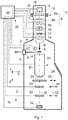
- Figure 1 (not to scale) is a highly schematic depiction of an embodiment of a charged-particle microscope M in which the present invention is implemented; more specifically, it shows an embodiment of a transmission-type microscope M, which, in this case, is a TEM/STEM (though, in the context of the current invention, it could just as validly be a SEM, or an ion-based microscope, for example).
- a transmission-type microscope M which, in this case, is a TEM/STEM (though, in the context of the current invention, it could just as validly be a SEM, or an ion-based microscope, for example).
- a small-emission-area source such as a CFEG electron source 4 produces a beam B of electrons that propagates along an electron-optical axis B' and traverses an electron-optical illuminator 6 (schematically depicted within a broken line), serving to direct/focus the electrons onto a chosen part of a specimen S (which may, for example, be (locally) thinned/planarized).
- This illuminator 6 will be discussed in more detail below.
- the specimen S is held on a specimen holder H that can be positioned in multiple degrees of freedom by a positioning device / stage A, which moves a cradle A' into which holder H is (removably) affixed; for example, the specimen holder H may comprise a finger that can be moved ( inter alia ) in the XY plane (see the depicted Cartesian coordinate system; typically, motion parallel to Z and tilt about X/Y will also be possible). Such movement allows different parts of the specimen S to be irradiated / imaged / inspected by the electron beam B traveling along axis B' (in the Z direction) (and/or allows scanning motion to be performed, as an alternative to beam scanning).
- an optional cooling device (not depicted) can be brought into intimate thermal contact with the specimen holder H, so as to maintain it (and the specimen S thereupon) at cryogenic temperatures, for example.
- the electron beam B will interact with the specimen S in such a manner as to cause various types of "stimulated” radiation to emanate from the specimen S, including (for example) secondary electrons, backscattered electrons, X-rays and optical radiation (cathodoluminescence).
- various types of "stimulated" radiation including (for example) secondary electrons, backscattered electrons, X-rays and optical radiation (cathodoluminescence).
- these radiation types can be detected with the aid of analysis device 22, which might be a combined scintillator/photomultiplier or EDX (Energy-Dispersive X-Ray Spectroscopy) module, for instance; in such a case, an image could be constructed using basically the same principle as in a SEM.
- an imaging system projection lens 24 which will generally comprise a variety of electrostatic / magnetic lenses, deflectors, correctors (such as stigmators), etc.
- this imaging system 24 can focus the transmitted electron flux onto a fluorescent screen 26, which, if desired, can be retracted/withdrawn (as schematically indicated by arrows 26') so as to get it out of the way of axis B'.
- An image (or diffractogram) of (part of) the specimen S will be formed by imaging system 24 on screen 26, and this may be viewed through viewing port 28 located in a suitable part of a wall of enclosure 2.
- the retraction mechanism for screen 26 may, for example, be mechanical and/or electrical in nature, and is not depicted here.
- controller 20 is connected to various illustrated components via control lines (buses) 20'.
- This controller 20 can provide a variety of functions, such as synchronizing actions, providing setpoints, processing signals, performing calculations, and displaying messages/information on a display device (not depicted).
- the (schematically depicted) controller 20 may be (partially) inside or outside the enclosure 2, and may have a unitary or composite structure, as desired.
- the interior of the enclosure 2 does not have to be kept at a strict vacuum; for example, in a so-called "Environmental TEM/STEM", a background atmosphere of a given gas is deliberately introduced / maintained within the enclosure 2.
- the skilled artisan will also understand that, in practice, it may be advantageous to confine the volume of enclosure 2 so that, where possible, it essentially hugs the axis B', taking the form of a small tube ( e.g . of the order of 1 cm in diameter) through which the employed electron beam passes, but widening out to accommodate structures such as the source 4, specimen holder H, screen 26, camera 30, camera 32, spectroscopic apparatus 34, etc.
- the illuminator 6 comprises (considered parallel to the propagation direction of beam B):
- the illuminator 6 additionally comprises:
- the source lens 8 is a compound lens comprising:
- source 4 and magnetic lens 8a may be regarded as forming an interchangeable assembly 4', which can be swapped out and replaced by a different such assembly.
- the properties of the magnetic lens 8a can be tuned to those of the chosen source 4 in such a manner that, regardless of the particular such assembly 4' chosen, the "lower" illuminator from electrostatic lens 8b downward does not have to be specifically matched each time to each different assembly 4', but can instead maintain a constant, generic architecture/configuration.
- Figure 2 shows a magnified, more detailed view of a portion of the subject of Figure 1 . More particularly, it shows (to approximate scale) the following components:
- the magnetic lens 8a is matched to the source 4 in such a way that the focal point 8d essentially coincides (relative to item 8b, for instance) with the position of a Schottky FEG, if one were to be used in this configuration.
Landscapes
- Chemical & Material Sciences (AREA)
- Analytical Chemistry (AREA)
- Physics & Mathematics (AREA)
- General Physics & Mathematics (AREA)
- Optics & Photonics (AREA)
- Analysing Materials By The Use Of Radiation (AREA)
- Investigating, Analyzing Materials By Fluorescence Or Luminescence (AREA)
Claims (7)
- Mikroskop (M) mit geladenen Teilchen, Folgendes umfassend:- ein Vakuumgehäuse (2);- eine Quelle (4) zum Erzeugen eines Strahls (B) geladener Teilchen;- einen Objekthalter (H) zum Halten eines Objekts (S);- eine Leuchte (6), die zwischen der Quelle (4) und dem Objekthalter (H) bereitgestellt ist und in einer Ausbreitungsrichtung des Strahls (B) Folgendes umfasst:- ein Quellenobjektiv (8), das dazu dient, eine Vergrößerung/Kollimation des Strahls unmittelbar nach einer Erzeugung durch die Quelle zu bewirken;- ein Kondensorsystem (10);- einen Detektor zum Erfassen von von dem Objekt (S) ausgehender Strahlung als Reaktion auf eine Bestrahlung durch den Strahl (B),wobei das Quellenobjektiv (8) ein mehrgliedriges Objektiv ist, das in der Ausbreitungsrichtung Folgendes umfasst:- ein magnetisches Objektiv (8a), das Permanentmagneten (16) umfasst, die außerhalb des Vakuumgehäuses (2) angeordnet sind, aber ein Magnetfeld innerhalb dessen erzeugen; und- ein variables elektrostatisches Objektiv (8b);
dadurch gekennzeichnet, dass das Quellenobjektiv (8) ferner einen Ausrichtungsstrahlablenker (8c) umfasst, der zwischen dem magnetischen Objektiv (8a) und dem elektrostatischen Objektiv (8b) bereitgestellt ist. - Mikroskop (M) nach Anspruch 1, wobei ein Monochromator zwischen dem elektrostatischen Objektiv (8b) und dem Kondensorsystem (10) bereitgestellt ist.
- Mikroskop (M) nach einem der Ansprüche 1-2, wobei das magnetische Objektiv (8a) ein magnetisches Joch (18) umfasst, das wenigstens teilweise innerhalb des Vakuumgehäuses (2) bereitgestellt ist und eine oder mehrere Komponenten der Quelle (4) umfasst.
- Mikroskop (M) nach Anspruch 3, wobei die Quelle (4) eine Extraktorelektrode (508) umfasst, die wenigstens teilweise in einem ersten Polstück des Jochs (18) enthalten ist.
- Mikroskop (M) nach Anspruch 3 oder 4, wobei die Quelle (4) eine Einschlusselektrode umfasst, die wenigstens teilweise in einem zweiten Polstück des Jochs (18) enthalten ist.
- Mikroskop (M) mit geladenen Teilchen nach einem der Ansprüche 1-5, wobei die Quelle (4) aus der Gruppe ausgewählt ist, die eine Feldemissionskaltkanone (Cold Field Emitter Gun - CFEG), eine Elektronenstoßionenquelle, eine Nanoöffnungsionenquelle (Nano Aperture Ion Source - NAIS), eine Flüssigmetallionenquelle (Liquid Metal Ion Source - LMIS) und eine Feldionisierungsquelle umfasst.
- Verfahren zum Betreiben eines Mikroskops (M) mit geladenen Teilchen, Folgendes umfassend:- Bereitstellen eines Objekts (S) auf einem Objekthalter (H);- Verwenden einer Quelle (4), um einen Strahl (B) geladener Teilchen zu erzeugen;- Führen des Strahls (B) durch eine Leuchte (6), die zwischen der Quelle (4) und dem Objekthalter (H) bereitgestellt ist und in einer Ausbreitungsrichtung des Strahls (B) Folgendes umfasst:- ein Quellenobjektiv (8), das dazu dient, eine Vergrößerung/Kollimation des Strahls unmittelbar nach einer Erzeugung durch die Quelle zu bewirken;- ein Kondensorsystem (10);- Bestrahlen des Objekts (S) mit dem Strahl (B), der aus der Leuchte (6) hervortritt;- Verwenden eines Detektors, um Strahlung zu erfassen, die von dem Objekt (S) als Reaktion auf die Bestrahlung ausgeht,- Konfigurieren und Verwenden des Quellenobjektivs (8) als ein mehrgliedriges Objektiv, das in der Ausbreitungsrichtung Folgendes umfasst:- ein magnetisches Objektiv (8a), die Permanentmagneten umfasst, die außerhalb des Vakuumgehäuses (2) angeordnet sind, aber ein Magnetfeld innerhalb dessen erzeugen; und- ein variables elektrostatisches Objektiv (8b);
wobei das Verfahren ferner ein Ausrichten des Strahls (B) an einem Ausrichtungsstrahlablenker (8c) umfasst, der zwischen dem magnetischen Objektiv (8a) und dem elektrostatischen Objektiv (8b) bereitgestellt ist
Applications Claiming Priority (1)
| Application Number | Priority Date | Filing Date | Title |
|---|---|---|---|
| US15/586,194 US10410827B2 (en) | 2017-05-03 | 2017-05-03 | Gun lens design in a charged particle microscope |
Publications (2)
| Publication Number | Publication Date |
|---|---|
| EP3399537A1 EP3399537A1 (de) | 2018-11-07 |
| EP3399537B1 true EP3399537B1 (de) | 2019-10-16 |
Family
ID=62104144
Family Applications (1)
| Application Number | Title | Priority Date | Filing Date |
|---|---|---|---|
| EP18170249.9A Active EP3399537B1 (de) | 2017-05-03 | 2018-05-01 | Kanonenlinsendesign in einem ladungsträgerteilchenmikroskop |
Country Status (6)
| Country | Link |
|---|---|
| US (1) | US10410827B2 (de) |
| EP (1) | EP3399537B1 (de) |
| JP (1) | JP7079135B2 (de) |
| KR (1) | KR102524584B1 (de) |
| CN (1) | CN108807120B (de) |
| BR (1) | BR102018009002A2 (de) |
Families Citing this family (5)
| Publication number | Priority date | Publication date | Assignee | Title |
|---|---|---|---|---|
| EP3550585B1 (de) * | 2018-04-05 | 2021-06-23 | FEI Company | Untersuchung dynamischer proben in einem transmissionsteilchenmikroskop |
| EP3881347A1 (de) | 2018-11-16 | 2021-09-22 | ASML Netherlands B.V. | Elektromagnetische zusammengesetzte linse und optisches system mit geladenen teilchen mit einer solchen linse |
| DE102020102314B4 (de) * | 2020-01-30 | 2022-02-10 | Carl Zeiss Microscopy Gmbh | Objektaufnahmebehälter, Objekthaltesystem mit einem Objektaufnahmebehälter, Strahlgerät und Gerät mit einem Objektaufnahmebehälter oder einem Objekthaltesystem sowie Verfahren zum Untersuchen, Analysieren und/oder Bearbeiten eines Objekts |
| EP3913654A1 (de) * | 2020-05-20 | 2021-11-24 | FEI Company | Axiale ausrichtungsanordnung und ladungsträgerteilchenmikroskop mit einer solchen ausrichtungsanordnung |
| US11417493B2 (en) * | 2020-12-18 | 2022-08-16 | Fei Company | Counter pole with permanent magnets |
Family Cites Families (20)
| Publication number | Priority date | Publication date | Assignee | Title |
|---|---|---|---|---|
| US2926254A (en) * | 1955-08-11 | 1960-02-23 | Vickers Electrical Co Ltd | Electron lenses |
| JPH0779016B2 (ja) * | 1990-08-13 | 1995-08-23 | 株式会社日立製作所 | 荷電粒子線装置 |
| KR970005769B1 (ko) | 1992-08-27 | 1997-04-19 | 가부시끼가이샤 도시바 | 자계 계침형 전자총 |
| JP2835265B2 (ja) * | 1992-08-27 | 1998-12-14 | 株式会社東芝 | 磁界界浸型電子銃及び磁界界浸型電子銃操作方法 |
| JP3325982B2 (ja) * | 1993-12-27 | 2002-09-17 | 株式会社東芝 | 磁界界浸型電子銃 |
| WO2000079565A1 (en) | 1999-06-22 | 2000-12-28 | Philips Electron Optics B.V. | Particle-optical apparatus including a particle source that can be switched between high brightness and large beam current |
| NL1023260C1 (nl) | 2003-04-24 | 2004-10-27 | Fei Co | Deeltjes-optisch apparaat met een permanent magnetische lens en een elektrostatische lens. |
| NL1025500C2 (nl) | 2004-02-17 | 2005-08-19 | Fei Co | Deeltjesbron met selecteerbare bundelstroom en energiespreiding. |
| NL1026006C2 (nl) * | 2004-04-22 | 2005-10-25 | Fei Co | Deeltjes-optisch apparaat voorzien van lenzen met permanent magnetisch materiaal. |
| JP2006216396A (ja) | 2005-02-04 | 2006-08-17 | Hitachi High-Technologies Corp | 荷電粒子線装置 |
| JP2006324119A (ja) | 2005-05-19 | 2006-11-30 | Hitachi Ltd | 電子銃 |
| US7446320B1 (en) * | 2005-08-17 | 2008-11-04 | Kla-Tencor Technologies Corproation | Electronically-variable immersion electrostatic lens |
| US7888654B2 (en) | 2007-01-24 | 2011-02-15 | Fei Company | Cold field emitter |
| EP2128885A1 (de) | 2008-05-26 | 2009-12-02 | FEI Company | Quelle für geladene Teilchen mit integriertem Energiefilter |
| EP2453461A1 (de) | 2010-11-10 | 2012-05-16 | FEI Company | Quelle für geladene Teilchen mit integriertem elektrostatischen Energiefilter |
| US8736170B1 (en) | 2011-02-22 | 2014-05-27 | Fei Company | Stable cold field emission electron source |
| US8779376B2 (en) | 2012-01-09 | 2014-07-15 | Fei Company | Determination of emission parameters from field emission sources |
| JP2015015200A (ja) * | 2013-07-08 | 2015-01-22 | 株式会社日立ハイテクノロジーズ | 電子銃および電子顕微鏡 |
| EP2827357A1 (de) * | 2013-07-18 | 2015-01-21 | Fei Company | Magnetische Linse zum Fokussieren eines Strahls geladener Teilchen |
| KR101633978B1 (ko) * | 2014-06-20 | 2016-06-28 | 한국표준과학연구원 | 모노크로메이터 및 이를 구비한 하전입자빔 장치 |
-
2017
- 2017-05-03 US US15/586,194 patent/US10410827B2/en active Active
-
2018
- 2018-04-24 KR KR1020180047606A patent/KR102524584B1/ko active Active
- 2018-04-27 CN CN201810393514.6A patent/CN108807120B/zh active Active
- 2018-05-01 EP EP18170249.9A patent/EP3399537B1/de active Active
- 2018-05-02 JP JP2018088536A patent/JP7079135B2/ja active Active
- 2018-05-03 BR BR102018009002-0A patent/BR102018009002A2/pt not_active Application Discontinuation
Non-Patent Citations (1)
| Title |
|---|
| None * |
Also Published As
| Publication number | Publication date |
|---|---|
| KR102524584B1 (ko) | 2023-04-21 |
| CN108807120B (zh) | 2020-07-10 |
| CN108807120A (zh) | 2018-11-13 |
| EP3399537A1 (de) | 2018-11-07 |
| KR20180122551A (ko) | 2018-11-13 |
| JP2018190723A (ja) | 2018-11-29 |
| JP7079135B2 (ja) | 2022-06-01 |
| BR102018009002A2 (pt) | 2018-11-21 |
| US10410827B2 (en) | 2019-09-10 |
| US20180323036A1 (en) | 2018-11-08 |
Similar Documents
| Publication | Publication Date | Title |
|---|---|---|
| EP3399537B1 (de) | Kanonenlinsendesign in einem ladungsträgerteilchenmikroskop | |
| EP3444836B1 (de) | Beugungsbilddetektion in einem ladungsträgerteilchenmikroskop | |
| JP7030549B2 (ja) | 荷電粒子源の放出雑音補正 | |
| US10157727B2 (en) | Aberration measurement in a charged particle microscope | |
| US11955310B2 (en) | Transmission charged particle microscope with an electron energy loss spectroscopy detector | |
| US9984852B1 (en) | Time-of-flight charged particle spectroscopy | |
| EP3401943B1 (de) | Innovative bildverarbeitung in der ladungsteilchenmikroskopie | |
| US11024483B2 (en) | Transmission charged particle microscope with adjustable beam energy spread | |
| US10559448B2 (en) | Transmission charged particle microscope with improved EELS/EFTEM module | |
| EP3477679B1 (de) | Verbesserte kryogene zelle zum anbringen einer probe in einem geladenen teilchenmikroskop |
Legal Events
| Date | Code | Title | Description |
|---|---|---|---|
| PUAI | Public reference made under article 153(3) epc to a published international application that has entered the european phase |
Free format text: ORIGINAL CODE: 0009012 |
|
| STAA | Information on the status of an ep patent application or granted ep patent |
Free format text: STATUS: THE APPLICATION HAS BEEN PUBLISHED |
|
| AK | Designated contracting states |
Kind code of ref document: A1 Designated state(s): AL AT BE BG CH CY CZ DE DK EE ES FI FR GB GR HR HU IE IS IT LI LT LU LV MC MK MT NL NO PL PT RO RS SE SI SK SM TR |
|
| AX | Request for extension of the european patent |
Extension state: BA ME |
|
| STAA | Information on the status of an ep patent application or granted ep patent |
Free format text: STATUS: REQUEST FOR EXAMINATION WAS MADE |
|
| 17P | Request for examination filed |
Effective date: 20190402 |
|
| RBV | Designated contracting states (corrected) |
Designated state(s): AL AT BE BG CH CY CZ DE DK EE ES FI FR GB GR HR HU IE IS IT LI LT LU LV MC MK MT NL NO PL PT RO RS SE SI SK SM TR |
|
| RIC1 | Information provided on ipc code assigned before grant |
Ipc: H01J 37/28 20060101ALN20190430BHEP Ipc: H01J 37/067 20060101ALI20190430BHEP Ipc: H01J 37/065 20060101AFI20190430BHEP Ipc: H01J 37/145 20060101ALI20190430BHEP |
|
| GRAP | Despatch of communication of intention to grant a patent |
Free format text: ORIGINAL CODE: EPIDOSNIGR1 |
|
| STAA | Information on the status of an ep patent application or granted ep patent |
Free format text: STATUS: GRANT OF PATENT IS INTENDED |
|
| RIC1 | Information provided on ipc code assigned before grant |
Ipc: H01J 37/28 20060101ALN20190524BHEP Ipc: H01J 37/067 20060101ALI20190524BHEP Ipc: H01J 37/065 20060101AFI20190524BHEP Ipc: H01J 37/145 20060101ALI20190524BHEP |
|
| INTG | Intention to grant announced |
Effective date: 20190612 |
|
| GRAS | Grant fee paid |
Free format text: ORIGINAL CODE: EPIDOSNIGR3 |
|
| GRAA | (expected) grant |
Free format text: ORIGINAL CODE: 0009210 |
|
| STAA | Information on the status of an ep patent application or granted ep patent |
Free format text: STATUS: THE PATENT HAS BEEN GRANTED |
|
| AK | Designated contracting states |
Kind code of ref document: B1 Designated state(s): AL AT BE BG CH CY CZ DE DK EE ES FI FR GB GR HR HU IE IS IT LI LT LU LV MC MK MT NL NO PL PT RO RS SE SI SK SM TR |
|
| REG | Reference to a national code |
Ref country code: GB Ref legal event code: FG4D |
|
| REG | Reference to a national code |
Ref country code: CH Ref legal event code: EP |
|
| REG | Reference to a national code |
Ref country code: DE Ref legal event code: R096 Ref document number: 602018000891 Country of ref document: DE |
|
| REG | Reference to a national code |
Ref country code: IE Ref legal event code: FG4D |
|
| REG | Reference to a national code |
Ref country code: AT Ref legal event code: REF Ref document number: 1192113 Country of ref document: AT Kind code of ref document: T Effective date: 20191115 |
|
| REG | Reference to a national code |
Ref country code: NL Ref legal event code: MP Effective date: 20191016 |
|
| REG | Reference to a national code |
Ref country code: LT Ref legal event code: MG4D |
|
| REG | Reference to a national code |
Ref country code: AT Ref legal event code: MK05 Ref document number: 1192113 Country of ref document: AT Kind code of ref document: T Effective date: 20191016 |
|
| PG25 | Lapsed in a contracting state [announced via postgrant information from national office to epo] |
Ref country code: AT Free format text: LAPSE BECAUSE OF FAILURE TO SUBMIT A TRANSLATION OF THE DESCRIPTION OR TO PAY THE FEE WITHIN THE PRESCRIBED TIME-LIMIT Effective date: 20191016 Ref country code: SE Free format text: LAPSE BECAUSE OF FAILURE TO SUBMIT A TRANSLATION OF THE DESCRIPTION OR TO PAY THE FEE WITHIN THE PRESCRIBED TIME-LIMIT Effective date: 20191016 Ref country code: LV Free format text: LAPSE BECAUSE OF FAILURE TO SUBMIT A TRANSLATION OF THE DESCRIPTION OR TO PAY THE FEE WITHIN THE PRESCRIBED TIME-LIMIT Effective date: 20191016 Ref country code: PL Free format text: LAPSE BECAUSE OF FAILURE TO SUBMIT A TRANSLATION OF THE DESCRIPTION OR TO PAY THE FEE WITHIN THE PRESCRIBED TIME-LIMIT Effective date: 20191016 Ref country code: GR Free format text: LAPSE BECAUSE OF FAILURE TO SUBMIT A TRANSLATION OF THE DESCRIPTION OR TO PAY THE FEE WITHIN THE PRESCRIBED TIME-LIMIT Effective date: 20200117 Ref country code: NO Free format text: LAPSE BECAUSE OF FAILURE TO SUBMIT A TRANSLATION OF THE DESCRIPTION OR TO PAY THE FEE WITHIN THE PRESCRIBED TIME-LIMIT Effective date: 20200116 Ref country code: BG Free format text: LAPSE BECAUSE OF FAILURE TO SUBMIT A TRANSLATION OF THE DESCRIPTION OR TO PAY THE FEE WITHIN THE PRESCRIBED TIME-LIMIT Effective date: 20200116 Ref country code: PT Free format text: LAPSE BECAUSE OF FAILURE TO SUBMIT A TRANSLATION OF THE DESCRIPTION OR TO PAY THE FEE WITHIN THE PRESCRIBED TIME-LIMIT Effective date: 20200217 Ref country code: FI Free format text: LAPSE BECAUSE OF FAILURE TO SUBMIT A TRANSLATION OF THE DESCRIPTION OR TO PAY THE FEE WITHIN THE PRESCRIBED TIME-LIMIT Effective date: 20191016 Ref country code: LT Free format text: LAPSE BECAUSE OF FAILURE TO SUBMIT A TRANSLATION OF THE DESCRIPTION OR TO PAY THE FEE WITHIN THE PRESCRIBED TIME-LIMIT Effective date: 20191016 Ref country code: NL Free format text: LAPSE BECAUSE OF FAILURE TO SUBMIT A TRANSLATION OF THE DESCRIPTION OR TO PAY THE FEE WITHIN THE PRESCRIBED TIME-LIMIT Effective date: 20191016 |
|
| PG25 | Lapsed in a contracting state [announced via postgrant information from national office to epo] |
Ref country code: HR Free format text: LAPSE BECAUSE OF FAILURE TO SUBMIT A TRANSLATION OF THE DESCRIPTION OR TO PAY THE FEE WITHIN THE PRESCRIBED TIME-LIMIT Effective date: 20191016 Ref country code: IS Free format text: LAPSE BECAUSE OF FAILURE TO SUBMIT A TRANSLATION OF THE DESCRIPTION OR TO PAY THE FEE WITHIN THE PRESCRIBED TIME-LIMIT Effective date: 20200224 Ref country code: RS Free format text: LAPSE BECAUSE OF FAILURE TO SUBMIT A TRANSLATION OF THE DESCRIPTION OR TO PAY THE FEE WITHIN THE PRESCRIBED TIME-LIMIT Effective date: 20191016 |
|
| PG25 | Lapsed in a contracting state [announced via postgrant information from national office to epo] |
Ref country code: AL Free format text: LAPSE BECAUSE OF FAILURE TO SUBMIT A TRANSLATION OF THE DESCRIPTION OR TO PAY THE FEE WITHIN THE PRESCRIBED TIME-LIMIT Effective date: 20191016 |
|
| REG | Reference to a national code |
Ref country code: DE Ref legal event code: R097 Ref document number: 602018000891 Country of ref document: DE |
|
| PG2D | Information on lapse in contracting state deleted |
Ref country code: IS |
|
| PG25 | Lapsed in a contracting state [announced via postgrant information from national office to epo] |
Ref country code: ES Free format text: LAPSE BECAUSE OF FAILURE TO SUBMIT A TRANSLATION OF THE DESCRIPTION OR TO PAY THE FEE WITHIN THE PRESCRIBED TIME-LIMIT Effective date: 20191016 Ref country code: RO Free format text: LAPSE BECAUSE OF FAILURE TO SUBMIT A TRANSLATION OF THE DESCRIPTION OR TO PAY THE FEE WITHIN THE PRESCRIBED TIME-LIMIT Effective date: 20191016 Ref country code: EE Free format text: LAPSE BECAUSE OF FAILURE TO SUBMIT A TRANSLATION OF THE DESCRIPTION OR TO PAY THE FEE WITHIN THE PRESCRIBED TIME-LIMIT Effective date: 20191016 Ref country code: DK Free format text: LAPSE BECAUSE OF FAILURE TO SUBMIT A TRANSLATION OF THE DESCRIPTION OR TO PAY THE FEE WITHIN THE PRESCRIBED TIME-LIMIT Effective date: 20191016 Ref country code: IS Free format text: LAPSE BECAUSE OF FAILURE TO SUBMIT A TRANSLATION OF THE DESCRIPTION OR TO PAY THE FEE WITHIN THE PRESCRIBED TIME-LIMIT Effective date: 20200216 |
|
| PLBE | No opposition filed within time limit |
Free format text: ORIGINAL CODE: 0009261 |
|
| STAA | Information on the status of an ep patent application or granted ep patent |
Free format text: STATUS: NO OPPOSITION FILED WITHIN TIME LIMIT |
|
| PG25 | Lapsed in a contracting state [announced via postgrant information from national office to epo] |
Ref country code: IT Free format text: LAPSE BECAUSE OF FAILURE TO SUBMIT A TRANSLATION OF THE DESCRIPTION OR TO PAY THE FEE WITHIN THE PRESCRIBED TIME-LIMIT Effective date: 20191016 Ref country code: SM Free format text: LAPSE BECAUSE OF FAILURE TO SUBMIT A TRANSLATION OF THE DESCRIPTION OR TO PAY THE FEE WITHIN THE PRESCRIBED TIME-LIMIT Effective date: 20191016 Ref country code: SK Free format text: LAPSE BECAUSE OF FAILURE TO SUBMIT A TRANSLATION OF THE DESCRIPTION OR TO PAY THE FEE WITHIN THE PRESCRIBED TIME-LIMIT Effective date: 20191016 |
|
| 26N | No opposition filed |
Effective date: 20200717 |
|
| PG25 | Lapsed in a contracting state [announced via postgrant information from national office to epo] |
Ref country code: SI Free format text: LAPSE BECAUSE OF FAILURE TO SUBMIT A TRANSLATION OF THE DESCRIPTION OR TO PAY THE FEE WITHIN THE PRESCRIBED TIME-LIMIT Effective date: 20191016 |
|
| PG25 | Lapsed in a contracting state [announced via postgrant information from national office to epo] |
Ref country code: MC Free format text: LAPSE BECAUSE OF FAILURE TO SUBMIT A TRANSLATION OF THE DESCRIPTION OR TO PAY THE FEE WITHIN THE PRESCRIBED TIME-LIMIT Effective date: 20191016 |
|
| REG | Reference to a national code |
Ref country code: BE Ref legal event code: MM Effective date: 20200531 |
|
| PG25 | Lapsed in a contracting state [announced via postgrant information from national office to epo] |
Ref country code: LU Free format text: LAPSE BECAUSE OF NON-PAYMENT OF DUE FEES Effective date: 20200501 |
|
| PG25 | Lapsed in a contracting state [announced via postgrant information from national office to epo] |
Ref country code: IE Free format text: LAPSE BECAUSE OF NON-PAYMENT OF DUE FEES Effective date: 20200501 |
|
| PG25 | Lapsed in a contracting state [announced via postgrant information from national office to epo] |
Ref country code: BE Free format text: LAPSE BECAUSE OF NON-PAYMENT OF DUE FEES Effective date: 20200531 |
|
| REG | Reference to a national code |
Ref country code: CH Ref legal event code: PL |
|
| PG25 | Lapsed in a contracting state [announced via postgrant information from national office to epo] |
Ref country code: LI Free format text: LAPSE BECAUSE OF NON-PAYMENT OF DUE FEES Effective date: 20210531 Ref country code: CH Free format text: LAPSE BECAUSE OF NON-PAYMENT OF DUE FEES Effective date: 20210531 |
|
| PG25 | Lapsed in a contracting state [announced via postgrant information from national office to epo] |
Ref country code: TR Free format text: LAPSE BECAUSE OF FAILURE TO SUBMIT A TRANSLATION OF THE DESCRIPTION OR TO PAY THE FEE WITHIN THE PRESCRIBED TIME-LIMIT Effective date: 20191016 Ref country code: MT Free format text: LAPSE BECAUSE OF FAILURE TO SUBMIT A TRANSLATION OF THE DESCRIPTION OR TO PAY THE FEE WITHIN THE PRESCRIBED TIME-LIMIT Effective date: 20191016 Ref country code: CY Free format text: LAPSE BECAUSE OF FAILURE TO SUBMIT A TRANSLATION OF THE DESCRIPTION OR TO PAY THE FEE WITHIN THE PRESCRIBED TIME-LIMIT Effective date: 20191016 |
|
| PG25 | Lapsed in a contracting state [announced via postgrant information from national office to epo] |
Ref country code: MK Free format text: LAPSE BECAUSE OF FAILURE TO SUBMIT A TRANSLATION OF THE DESCRIPTION OR TO PAY THE FEE WITHIN THE PRESCRIBED TIME-LIMIT Effective date: 20191016 |
|
| PGFP | Annual fee paid to national office [announced via postgrant information from national office to epo] |
Ref country code: DE Payment date: 20250416 Year of fee payment: 8 |
|
| PGFP | Annual fee paid to national office [announced via postgrant information from national office to epo] |
Ref country code: FR Payment date: 20250506 Year of fee payment: 8 |
|
| PGFP | Annual fee paid to national office [announced via postgrant information from national office to epo] |
Ref country code: CZ Payment date: 20250428 Year of fee payment: 8 |
|
| PGFP | Annual fee paid to national office [announced via postgrant information from national office to epo] |
Ref country code: GB Payment date: 20260312 Year of fee payment: 9 |