EP3399639A1 - Wechselrichter - Google Patents
Wechselrichter Download PDFInfo
- Publication number
- EP3399639A1 EP3399639A1 EP16881606.4A EP16881606A EP3399639A1 EP 3399639 A1 EP3399639 A1 EP 3399639A1 EP 16881606 A EP16881606 A EP 16881606A EP 3399639 A1 EP3399639 A1 EP 3399639A1
- Authority
- EP
- European Patent Office
- Prior art keywords
- terminal
- power device
- wiring
- electrolytic capacitor
- circuit board
- Prior art date
- Legal status (The legal status is an assumption and is not a legal conclusion. Google has not performed a legal analysis and makes no representation as to the accuracy of the status listed.)
- Granted
Links
Images


Classifications
-
- H—ELECTRICITY
- H05—ELECTRIC TECHNIQUES NOT OTHERWISE PROVIDED FOR
- H05K—PRINTED CIRCUITS; CASINGS OR CONSTRUCTIONAL DETAILS OF ELECTRIC APPARATUS; MANUFACTURE OF ASSEMBLAGES OF ELECTRICAL COMPONENTS
- H05K1/00—Printed circuits
- H05K1/02—Details
- H05K1/0201—Thermal arrangements, e.g. for cooling, heating or preventing overheating
- H05K1/0203—Cooling of mounted components
- H05K1/0204—Cooling of mounted components using means for thermal conduction connection in the thickness direction of the substrate
- H05K1/0206—Cooling of mounted components using means for thermal conduction connection in the thickness direction of the substrate by printed thermal vias
-
- H—ELECTRICITY
- H01—ELECTRIC ELEMENTS
- H01G—CAPACITORS; CAPACITORS, RECTIFIERS, DETECTORS, SWITCHING DEVICES, LIGHT-SENSITIVE OR TEMPERATURE-SENSITIVE DEVICES OF THE ELECTROLYTIC TYPE
- H01G9/00—Electrolytic capacitors, rectifiers, detectors, switching devices, light-sensitive or temperature-sensitive devices; Processes of their manufacture
- H01G9/0003—Protection against electric or thermal overload; cooling arrangements; means for avoiding the formation of cathode films
-
- H—ELECTRICITY
- H02—GENERATION; CONVERSION OR DISTRIBUTION OF ELECTRIC POWER
- H02M—APPARATUS FOR CONVERSION BETWEEN AC AND AC, BETWEEN AC AND DC, OR BETWEEN DC AND DC, AND FOR USE WITH MAINS OR SIMILAR POWER SUPPLY SYSTEMS; CONVERSION OF DC OR AC INPUT POWER INTO SURGE OUTPUT POWER; CONTROL OR REGULATION THEREOF
- H02M7/00—Conversion of AC power input into DC power output; Conversion of DC power input into AC power output
- H02M7/003—Constructional details, e.g. physical layout, assembly, wiring or busbar connections
-
- H—ELECTRICITY
- H02—GENERATION; CONVERSION OR DISTRIBUTION OF ELECTRIC POWER
- H02M—APPARATUS FOR CONVERSION BETWEEN AC AND AC, BETWEEN AC AND DC, OR BETWEEN DC AND DC, AND FOR USE WITH MAINS OR SIMILAR POWER SUPPLY SYSTEMS; CONVERSION OF DC OR AC INPUT POWER INTO SURGE OUTPUT POWER; CONTROL OR REGULATION THEREOF
- H02M7/00—Conversion of AC power input into DC power output; Conversion of DC power input into AC power output
- H02M7/42—Conversion of DC power input into AC power output without possibility of reversal
- H02M7/44—Conversion of DC power input into AC power output without possibility of reversal by static converters
- H02M7/48—Conversion of DC power input into AC power output without possibility of reversal by static converters using discharge tubes with control electrode or semiconductor devices with control electrode
-
- H—ELECTRICITY
- H05—ELECTRIC TECHNIQUES NOT OTHERWISE PROVIDED FOR
- H05K—PRINTED CIRCUITS; CASINGS OR CONSTRUCTIONAL DETAILS OF ELECTRIC APPARATUS; MANUFACTURE OF ASSEMBLAGES OF ELECTRICAL COMPONENTS
- H05K1/00—Printed circuits
- H05K1/02—Details
- H05K1/0201—Thermal arrangements, e.g. for cooling, heating or preventing overheating
- H05K1/0203—Cooling of mounted components
-
- H—ELECTRICITY
- H05—ELECTRIC TECHNIQUES NOT OTHERWISE PROVIDED FOR
- H05K—PRINTED CIRCUITS; CASINGS OR CONSTRUCTIONAL DETAILS OF ELECTRIC APPARATUS; MANUFACTURE OF ASSEMBLAGES OF ELECTRICAL COMPONENTS
- H05K1/00—Printed circuits
- H05K1/18—Printed circuits structurally associated with non-printed electric components
- H05K1/181—Printed circuits structurally associated with non-printed electric components associated with surface mounted components
-
- H—ELECTRICITY
- H05—ELECTRIC TECHNIQUES NOT OTHERWISE PROVIDED FOR
- H05K—PRINTED CIRCUITS; CASINGS OR CONSTRUCTIONAL DETAILS OF ELECTRIC APPARATUS; MANUFACTURE OF ASSEMBLAGES OF ELECTRICAL COMPONENTS
- H05K7/00—Constructional details common to different types of electric apparatus
- H05K7/20—Modifications to facilitate cooling, ventilating, or heating
- H05K7/2089—Modifications to facilitate cooling, ventilating, or heating for power electronics, e.g. for inverters for controlling motor
- H05K7/209—Heat transfer by conduction from internal heat source to heat radiating structure
-
- H—ELECTRICITY
- H01—ELECTRIC ELEMENTS
- H01G—CAPACITORS; CAPACITORS, RECTIFIERS, DETECTORS, SWITCHING DEVICES, LIGHT-SENSITIVE OR TEMPERATURE-SENSITIVE DEVICES OF THE ELECTROLYTIC TYPE
- H01G9/00—Electrolytic capacitors, rectifiers, detectors, switching devices, light-sensitive or temperature-sensitive devices; Processes of their manufacture
- H01G9/28—Structural combinations of electrolytic capacitors, rectifiers, detectors, switching devices with other electric components not covered by this subclass
-
- H—ELECTRICITY
- H05—ELECTRIC TECHNIQUES NOT OTHERWISE PROVIDED FOR
- H05K—PRINTED CIRCUITS; CASINGS OR CONSTRUCTIONAL DETAILS OF ELECTRIC APPARATUS; MANUFACTURE OF ASSEMBLAGES OF ELECTRICAL COMPONENTS
- H05K2201/00—Indexing scheme relating to printed circuits covered by H05K1/00
- H05K2201/10—Details of components or other objects attached to or integrated in a printed circuit board
- H05K2201/10007—Types of components
- H05K2201/10015—Non-printed capacitor
-
- H—ELECTRICITY
- H05—ELECTRIC TECHNIQUES NOT OTHERWISE PROVIDED FOR
- H05K—PRINTED CIRCUITS; CASINGS OR CONSTRUCTIONAL DETAILS OF ELECTRIC APPARATUS; MANUFACTURE OF ASSEMBLAGES OF ELECTRICAL COMPONENTS
- H05K2201/00—Indexing scheme relating to printed circuits covered by H05K1/00
- H05K2201/10—Details of components or other objects attached to or integrated in a printed circuit board
- H05K2201/10431—Details of mounted components
- H05K2201/10507—Involving several components
- H05K2201/10545—Related components mounted on both sides of the PCB
Definitions
- This invention relates to a technique for dissipating heat of a power device, and particularly to a technique for dissipating, on a printed circuit board, heat of a power device mounted together with an electrolytic capacitor on the printed circuit board.
- the inverter generally includes a power device used for power conversion, and a smoothing capacitor.
- the capacitance of the smoothing capacitor is normally selected approximately from several tens to several hundreds ⁇ F.
- the electrolytic capacitor is used as the smoothing capacitor. Since the electrolytic capacitor having such degree of capacitance is not only high but also large in the width direction, the electrolytic capacitor disposed horizontally occupies a large region along the substrate on which the electrolytic capacitor is mounted.
- the outer shell of the electrolytic capacitor is generally made of a metal covered with a film. Since the metal has the same potential as that of the negative side of the capacitor, the potential of the metal in an inverter is set to a ground potential (a potential of a lower-potential side of DC buses).
- disposing a component handling a generally-called heavy current near the electrolytic capacitor is not preferable from the viewpoint of securing an insulation distance.
- disposing the electrolytic capacitor horizontally which solely contributes to reduction in the thickness, does not necessarily contribute to miniaturization of the electrical equipment.
- a heat dissipation metal for dissipating heat of a power device also occupies the large region.
- a structure for dissipating, on a printed circuit board, heat of a power device mounted together with an electrolytic capacitor on the printed circuit board has a tendency to occupy the large region.
- this invention provides a technique for dissipating heat of a power device mounted on a printed circuit board together with an electrolytic capacitor without occupying a large region on a surface along the printed circuit board.
- An inverter includes: a printed circuit board (9); an electrolytic capacitor (4) horizontally disposed and mounted on one surface (90a) of the printed circuit board; and a power device (1) mounted on the printed circuit board and including a terminal (11) connected to a terminal (41) of the electrolytic capacitor.
- the printed circuit board includes: a plate-shaped substrate (90) with insulation properties; and a metal object (2) connecting the terminal of the electrolytic capacitor to the terminal of the power device, the metal object including a heat dissipating portion (22) facing the electrolytic capacitor on the one surface and dissipating heat generated by the power device.
- the second aspect of the inverter of this invention is the first aspect thereof in which the metal object (2) further includes a wiring (21) connecting the terminal (11) of the power device to the terminal (41) of the electrolytic capacitor (4).
- the heat dissipating portion (22) is provided to branch off from the wiring, and is connected to the terminal (11) of the power device and the terminal of the electrolytic capacitor through the wiring at a place (20, 23) of the branching.
- the third aspect of the inverter of this invention is the second aspect thereof in which the power device (1) is disposed on the one surface (90a), the metal object (2) is of an even thickness, and the heat dissipating portion (22) is wider than a pattern width required for the wiring (21).
- the fourth aspect of the inverter of this invention is the third aspect thereof in which the heat dissipating portion (22) includes a portion exceeding a width defined by 1 mm/A at a maximum value of a current flowing through the wiring.
- the fifth aspect of the inverter of this invention is the second aspect thereof in which the power device (1) is disposed on another surface (90b) of the printed circuit board, and the metal object further includes a through hole (23) penetrating the substrate (90) to connect the wiring (21) to the heat dissipating portion (22).
- heat of the power device mounted on the printed circuit board together with the electrolytic capacitor will be dissipated without occupying a large region on a surface along the printed circuit board.
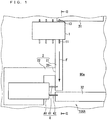
- FIG. 1 is a plan view exemplifying a structure of an inverter 100A according to the first embodiment.
- FIG. 2 is a cross-sectional view on arrows at positions II-II of FIG. 1 .
- the inverter 100A includes a power device 1, an electrolytic capacitor 4, and a printed circuit board 9.
- the power device 1 and the electrolytic capacitor 4 are mounted on the printed circuit board 9.
- the electrolytic capacitor 4 is horizontally disposed and mounted on one surface 90a of the printed circuit board 9.
- the electrolytic capacitor 4 includes a main body 40 and terminals 41 and 42.
- the power device 1 includes a plurality of terminals one of which is a terminal 11 connected to the terminal 41 of the electrolytic capacitor 4. According to the first embodiment, the power device 1 is also disposed on the surface 90a.
- the printed circuit board 9 includes a substrate 90 and a metal object 2.
- the substrate 90 has insulation properties and is plate-shaped.
- the metal object 2 includes a heat dissipating portion 22.
- the heat dissipating portion 22 faces the electrolytic capacitor 4 on the surface 90a, and dissipates heat generated by the power device 1.
- Another surface 90b (a surface opposite to the surface 90a) of the printed circuit board 9 has nothing to do with the structure for obtaining the advantages in the first embodiment.
- the metal object 2 further includes a wiring 21 according to the first embodiment.
- the wiring 21 connects the terminal 11 to the terminal 41. Specifically, one end of the wiring 21 is connected to the terminal 11, and the other end of the wiring 21 is connected to the terminal 41.
- the heat dissipating portion 22 is provided to branch off from the wiring 21 at a place 20. Thus, it can be said that the heat dissipating portion 22 is connected to both the terminals 11 and 41 through the wiring 21.
- the branching place 20 is preferably closer to the terminal 11 than a connection point between the wiring 21 and the terminal 41.
- Wirings 31 and 32 are also provided on the surface 90a.
- the power device 1 includes, other than the terminal 11, a terminal 13 connected to the wiring 31.
- the terminal 42 is connected to the wiring 32.
- the power device 1 includes terminals other than the terminals 11 and 13, the connection relationship between such terminals and wirings (not illustrated) is irrelevant to the first embodiment. Thus, the description thereof will be omitted.
- FIG. 3 illustrates an electric equivalent circuit of the metal object 2 illustrated in FIGS. 1 and 2 .
- An electric resistance of the wiring 21 between the terminal 11 and the place 20 is depicted as an equivalent resistor R21a.
- An electric resistance of the wiring 21 between the place 20 and the terminal 41 is depicted as an equivalent resistor R21b.
- a total electric resistance of the wiring 21 is depicted as an equivalent resistor R21 by the series connection of the equivalent resistors R21a and R21b.
- An arrow F in FIG. 1 schematically illustrates a current flowing from the terminal 11 to the terminal 41. Since the heat dissipating portion 22 branches off from the wiring 21 closer to the terminal 11 than the connection point between the wiring 21 and the terminal 41, the current is hardly diverted to the heat dissipating portion 22 but flows from the terminal 11 to the terminal 41.
- FIG. 3 illustrates connection of one end of the equivalent resistor R22 to the equivalent resistors R21a and R21b at the place 20 using solid lines, and also connection of the other end of the equivalent resistor R22 to the terminal 41 using a broken line.
- the heat dissipating portion 22 may branch off from the wiring 21 at a plurality of portions. In other words, the heat dissipating portion 22 may be jointed to the wiring 21 at the portions. This is because the current is hardly diverted to the heat dissipating portion 22 also with such a structure.
- the heat dissipating portion 22 does not function as a current path between the terminals 11 and 41. However, the heat dissipating portion 22 functions as dissipating heat of the power device 1 through the terminal 11 and the wiring 21. Since the heat dissipating portion 22 faces the main body 40 of the electrolytic capacitor 4, the region occupied by the heat dissipating portion 22 has an overlap with the region occupied by the main body 40 along the surface 90a.
- the heat of the power device 1 mounted together with the electrolytic capacitor 4 on the printed circuit board 9 can be dissipated without occupying a large region on the surface 90a along the printed circuit board 9.
- the heat dissipating portion 22 faces the main body 40 of the electrolytic capacitor 4, the heat dissipating portion 22 preferably has the same potential as that of the negative side of the electrolytic capacitor 4, i.e., the ground potential (the potential of the lower-potential side of DC buses). This is possible by using the wiring 21 as the lower-potential side of the buses of the inverter 100A. In other words, both the terminal 11 of the power device 1 and the terminal 41 of the electrolytic capacitor 4 are terminals on the lower-potential side of the DC buses of the inverter 100A.
- the wiring 32 is used as a bus on a higher-potential side of the DC buses of the inverter 100A.
- both of the wirings 31 and 32 may be used as the bus on the higher-potential side so that the terminal 13 should be connected to a high potential end of the inverter 100A.
- the metal object 2 is normally of an even thickness to avoid complexity in the manufacturing processes. Since the heat dissipating portion 22 as well as the wiring 21 is a component of the metal object 2, both the heat dissipating portion 22 and the wiring 21 are normally of even thickness.
- the pattern width of the wiring 21 is preferably set to a value defined by 1 mm/A at the maximum value of a current flowing through the wiring 21 (exemplified by the arrow F in FIG. 1 ).
- the standard MIL-STD-257A defines allowable current values each corresponding to the thickness of a wiring (the thickness of copper foil) and temperature rise in the printed circuit board 9.
- the pattern width and the allowable value are not completely in a direct proportional relationship, it is understood that a temperature rise value falls within 10 degrees centigrade when 1 mm/A is used as a design value.
- the heat dissipating portion 22 is preferably provided widely on the surface 90a. Although the heat dissipating portion 22 does not function as a current path between the terminals 11 and 41, the heat dissipating portion 22 is preferably wider than the pattern width required for the wiring 21 as a current path. In other words, the heat dissipating portion 22 preferably includes a portion exceeding the pattern width defined by 1 mm/A.
- a wiring pattern is not set to be wider than the assumed current density from the viewpoint of reducing materials.
- the pattern width of the heat dissipating portion 22 is preferably set wider from the viewpoint of dissipating heat.
- FIGS. 4 and 5 illustrate a top view and a bottom view, respectively, for exemplifying a structure of an inverter 100B according to the second embodiment.
- FIG. 6 is a cross-sectional view on arrows at positions VI-VI of FIG. 4 .
- the inverter 100B includes the power device 1, the electrolytic capacitor 4, and the printed circuit board 9.
- the power device 1 and the electrolytic capacitor 4 are mounted on the printed circuit board 9.
- the electrolytic capacitor 4 is horizontally disposed and mounted on the one surface 90a of the printed circuit board 9.
- the electrolytic capacitor 4 includes the main body 40 and the terminals 41 and 42.
- the power device 1 includes a plurality of terminals one of which is the terminal 11 connected to the terminal 41 of the electrolytic capacitor 4. According to the second embodiment, the power device 1 is disposed on a surface 90b.
- FIG. 4 has been used as a plan view seen from the surface 90a side as the top view
- FIG. 5 has been used as a plan view seen from the surface 90b side as the bottom view.
- the printed circuit board 9 includes the substrate 90 and the metal object 2.
- the substrate 90 has insulation properties and is plate-shaped.
- the metal object 2 includes the wiring 21, the heat dissipating portion 22, and through holes 23 and 24.
- the heat dissipating portion 22 faces the electrolytic capacitor 4 on the surface 90a, and dissipates heat generated by the power device 1.
- the wiring 21 is provided on the surface 90b, and is connected to the terminal 11.
- the through hole 24 penetrates the substrate 90 to connect the wiring 21 to the terminal 41.
- the wiring 21 connects the terminal 11 to the terminal 41 through the through hole 24.
- the heat dissipating portion 22 is provided on the surface 90a to face the electrolytic capacitor 4, and dissipates heat generated by the power device 1. Specifically, the heat dissipating portion 22 is connected to the wiring 21 through the through hole 23 that penetrates the substrate 90.
- the heat dissipating portion 22 does not function as a current path between the terminals 11 and 41 but functions as dissipating heat of the power device 1 through the terminal 11, the wiring 21, and the through hole 23 according to the second embodiment similarly as the first embodiment. Since the heat dissipating portion 22 faces the main body 40 of the electrolytic capacitor 4, the region occupied by the heat dissipating portion 22 has an overlap with the region occupied by the main body 40 along the surface 90a.
- the heat of the power device 1 mounted together with the electrolytic capacitor 4 on the printed circuit board 9 can be dissipated without occupying a large region on the surface 90a along the printed circuit board 9, similarly as the first embodiment.
- the wiring 31 is provided on the surface 90b, and the wiring 32 is provided on the surface 90a.
- the power device 1 includes, other than the terminal 11, the terminal 13 connected to the wiring 31.
- the terminal 42 is connected to the wiring 32.
- the wirings 31 and 32 are connected through a through hole (not illustrated).
- the power device 1 includes terminals other than the terminals 11 and 13, the connection relationship between such terminals and wirings (not illustrated) is irrelevant to the second embodiment. Thus, the description thereof will be omitted.
Landscapes
- Engineering & Computer Science (AREA)
- Microelectronics & Electronic Packaging (AREA)
- Power Engineering (AREA)
- Physics & Mathematics (AREA)
- Thermal Sciences (AREA)
- Inverter Devices (AREA)
Applications Claiming Priority (2)
| Application Number | Priority Date | Filing Date | Title |
|---|---|---|---|
| JP2015256553A JP6098705B1 (ja) | 2015-12-28 | 2015-12-28 | インバータ |
| PCT/JP2016/086374 WO2017115627A1 (ja) | 2015-12-28 | 2016-12-07 | インバータ |
Publications (3)
| Publication Number | Publication Date |
|---|---|
| EP3399639A1 true EP3399639A1 (de) | 2018-11-07 |
| EP3399639A4 EP3399639A4 (de) | 2019-08-14 |
| EP3399639B1 EP3399639B1 (de) | 2020-03-04 |
Family
ID=58363145
Family Applications (1)
| Application Number | Title | Priority Date | Filing Date |
|---|---|---|---|
| EP16881606.4A Active EP3399639B1 (de) | 2015-12-28 | 2016-12-07 | Wechselrichter |
Country Status (6)
| Country | Link |
|---|---|
| US (1) | US10305391B2 (de) |
| EP (1) | EP3399639B1 (de) |
| JP (1) | JP6098705B1 (de) |
| CN (1) | CN108450048B (de) |
| ES (1) | ES2794570T3 (de) |
| WO (1) | WO2017115627A1 (de) |
Cited By (2)
| Publication number | Priority date | Publication date | Assignee | Title |
|---|---|---|---|---|
| EP3905288A3 (de) * | 2020-04-29 | 2021-11-10 | Samsung Electronics Co., Ltd. | Horizontal montiertes kondensatormodul |
| US11856700B2 (en) | 2020-04-29 | 2023-12-26 | Samsung Electronics Co., Ltd. | Horizontally mounted capacitor module and electronic device including same |
Families Citing this family (1)
| Publication number | Priority date | Publication date | Assignee | Title |
|---|---|---|---|---|
| JP7590919B2 (ja) * | 2021-05-17 | 2024-11-27 | 株式会社日立製作所 | 電力変換装置 |
Family Cites Families (22)
| Publication number | Priority date | Publication date | Assignee | Title |
|---|---|---|---|---|
| US5016139A (en) * | 1989-09-06 | 1991-05-14 | Whelen Technologies, Inc. | Electronic power supply with enhanced heat transfer characteristics |
| JPH10336985A (ja) | 1997-06-05 | 1998-12-18 | Matsushita Electric Ind Co Ltd | ブラシレスモータにおける駆動回路の放熱装置 |
| US6212086B1 (en) * | 1998-05-22 | 2001-04-03 | Intel Corporation | Packaging of a DC-to-DC converter |
| US6257329B1 (en) * | 1998-08-17 | 2001-07-10 | Alfiero Balzano | Thermal management system |
| US6212071B1 (en) * | 1999-08-20 | 2001-04-03 | Lucent Technologies, Inc. | Electrical circuit board heat dissipation system |
| JP3923703B2 (ja) * | 2000-03-29 | 2007-06-06 | ローム株式会社 | 放熱手段を有するプリント配線板 |
| JP3899844B2 (ja) * | 2001-05-15 | 2007-03-28 | 松下電器産業株式会社 | 電源回路 |
| JP2004007951A (ja) * | 2002-04-18 | 2004-01-08 | Canon Inc | スイッチング電源装置 |
| JP3847691B2 (ja) | 2002-09-26 | 2006-11-22 | 三菱電機株式会社 | 電力用半導体装置 |
| US6930885B2 (en) * | 2002-12-23 | 2005-08-16 | Eastman Kodak Company | Densely packed electronic assemblage with heat removing element |
| JP4507739B2 (ja) | 2004-07-26 | 2010-07-21 | パナソニック株式会社 | 横置き型面実装電解コンデンサ |
| JP4859443B2 (ja) * | 2005-11-17 | 2012-01-25 | 日立オートモティブシステムズ株式会社 | 電力変換装置 |
| JP5517650B2 (ja) * | 2010-02-01 | 2014-06-11 | 三菱重工業株式会社 | インバータ一体型電動圧縮機 |
| JP4958990B2 (ja) * | 2010-05-06 | 2012-06-20 | 三菱電機株式会社 | 車載用電力変換装置 |
| CN201708703U (zh) * | 2010-05-13 | 2011-01-12 | 深圳市麦格米特电气技术有限公司 | 一种交流适配器电路板 |
| CN201878031U (zh) * | 2010-08-13 | 2011-06-22 | 马成照 | 一种逆变器结构 |
| CN201928509U (zh) * | 2010-11-15 | 2011-08-10 | 芯通科技(成都)有限公司 | 安装在系统机箱内的射频功放pcb板及系统机箱 |
| CN202103943U (zh) * | 2011-05-27 | 2012-01-04 | 乐健线路板(珠海)有限公司 | 带有金属微散热器的印刷电路板 |
| JP2013187998A (ja) * | 2012-03-07 | 2013-09-19 | Nissan Motor Co Ltd | 電力変換装置 |
| US9642289B2 (en) * | 2013-09-19 | 2017-05-02 | Infineon Technologies Austria Ag | Power supply and method |
| JP6349807B2 (ja) * | 2014-03-14 | 2018-07-04 | オムロン株式会社 | 電子機器 |
| JP6252873B2 (ja) * | 2015-03-27 | 2017-12-27 | 株式会社オートネットワーク技術研究所 | 車載配電基板、電気接続箱および充放電コントローラ |
-
2015
- 2015-12-28 JP JP2015256553A patent/JP6098705B1/ja active Active
-
2016
- 2016-12-07 US US15/779,673 patent/US10305391B2/en active Active
- 2016-12-07 WO PCT/JP2016/086374 patent/WO2017115627A1/ja not_active Ceased
- 2016-12-07 ES ES16881606T patent/ES2794570T3/es active Active
- 2016-12-07 CN CN201680067150.1A patent/CN108450048B/zh active Active
- 2016-12-07 EP EP16881606.4A patent/EP3399639B1/de active Active
Cited By (2)
| Publication number | Priority date | Publication date | Assignee | Title |
|---|---|---|---|---|
| EP3905288A3 (de) * | 2020-04-29 | 2021-11-10 | Samsung Electronics Co., Ltd. | Horizontal montiertes kondensatormodul |
| US11856700B2 (en) | 2020-04-29 | 2023-12-26 | Samsung Electronics Co., Ltd. | Horizontally mounted capacitor module and electronic device including same |
Also Published As
| Publication number | Publication date |
|---|---|
| JP6098705B1 (ja) | 2017-03-22 |
| US10305391B2 (en) | 2019-05-28 |
| EP3399639A4 (de) | 2019-08-14 |
| ES2794570T3 (es) | 2020-11-18 |
| EP3399639B1 (de) | 2020-03-04 |
| CN108450048A (zh) | 2018-08-24 |
| JP2017121124A (ja) | 2017-07-06 |
| CN108450048B (zh) | 2019-06-18 |
| US20180359846A1 (en) | 2018-12-13 |
| WO2017115627A1 (ja) | 2017-07-06 |
Similar Documents
| Publication | Publication Date | Title |
|---|---|---|
| US7839645B2 (en) | Module having at least two surfaces and at least one thermally conductive layer therebetween | |
| CN103796488B (zh) | 用于电基板的冷却装置 | |
| US10504813B2 (en) | Heat sink assemblies for surface mounted devices | |
| US9906154B2 (en) | Power conversion unit and power conversion device | |
| US9839128B2 (en) | Solder void reduction between electronic packages and printed circuit boards | |
| US20140198461A1 (en) | Low profile inductors for high density circuit boards | |
| US6618266B2 (en) | Method for high-density, low-via-count, decoupling capacitor placement | |
| US10031562B2 (en) | Cooling electronic components and supplying power to the electronic components | |
| EP3399639B1 (de) | Wechselrichter | |
| CN111418141A (zh) | 紧凑型热效率牵引电机逆变器 | |
| Gautam et al. | A comparison of thermal vias patterns used for thermal management in power converter | |
| WO2020155270A1 (en) | A power converter | |
| CN205670879U (zh) | 电路板 | |
| JP2014207370A (ja) | プリント基板 | |
| US11711897B2 (en) | Power conversion device | |
| US8625299B2 (en) | Circuit board with even current distribution | |
| US10219375B2 (en) | Hybrid circuit assembly | |
| CN103906356B (zh) | 用于印刷电路板结构中嵌入器件的系统和方法 | |
| KR102093893B1 (ko) | 고전류 회로 기판 | |
| US10728999B2 (en) | Circuit boards and method to manufacture circuit boards | |
| EP3319407A1 (de) | Modulare stromversorgung | |
| US20260025907A1 (en) | Power module using terminals of passive component as vias | |
| EP2200408A1 (de) | Platinenvorrichtung, insbesondere für eine stromverbrauchende Vorrichtung in einem Kraftfahrzeug | |
| KR20180013669A (ko) | 하이브리드 pcb 제조 방법 및 그 방법에 의해 제조된 하이브리드 pcb |
Legal Events
| Date | Code | Title | Description |
|---|---|---|---|
| STAA | Information on the status of an ep patent application or granted ep patent |
Free format text: STATUS: THE INTERNATIONAL PUBLICATION HAS BEEN MADE |
|
| PUAI | Public reference made under article 153(3) epc to a published international application that has entered the european phase |
Free format text: ORIGINAL CODE: 0009012 |
|
| STAA | Information on the status of an ep patent application or granted ep patent |
Free format text: STATUS: REQUEST FOR EXAMINATION WAS MADE |
|
| 17P | Request for examination filed |
Effective date: 20180608 |
|
| AK | Designated contracting states |
Kind code of ref document: A1 Designated state(s): AL AT BE BG CH CY CZ DE DK EE ES FI FR GB GR HR HU IE IS IT LI LT LU LV MC MK MT NL NO PL PT RO RS SE SI SK SM TR |
|
| AX | Request for extension of the european patent |
Extension state: BA ME |
|
| DAV | Request for validation of the european patent (deleted) | ||
| DAX | Request for extension of the european patent (deleted) | ||
| A4 | Supplementary search report drawn up and despatched |
Effective date: 20190716 |
|
| RIC1 | Information provided on ipc code assigned before grant |
Ipc: H02M 7/48 20070101AFI20190710BHEP Ipc: H05K 7/20 20060101ALI20190710BHEP |
|
| GRAP | Despatch of communication of intention to grant a patent |
Free format text: ORIGINAL CODE: EPIDOSNIGR1 |
|
| STAA | Information on the status of an ep patent application or granted ep patent |
Free format text: STATUS: GRANT OF PATENT IS INTENDED |
|
| INTG | Intention to grant announced |
Effective date: 20191119 |
|
| GRAS | Grant fee paid |
Free format text: ORIGINAL CODE: EPIDOSNIGR3 |
|
| GRAA | (expected) grant |
Free format text: ORIGINAL CODE: 0009210 |
|
| STAA | Information on the status of an ep patent application or granted ep patent |
Free format text: STATUS: THE PATENT HAS BEEN GRANTED |
|
| AK | Designated contracting states |
Kind code of ref document: B1 Designated state(s): AL AT BE BG CH CY CZ DE DK EE ES FI FR GB GR HR HU IE IS IT LI LT LU LV MC MK MT NL NO PL PT RO RS SE SI SK SM TR |
|
| REG | Reference to a national code |
Ref country code: GB Ref legal event code: FG4D |
|
| REG | Reference to a national code |
Ref country code: CH Ref legal event code: EP |
|
| REG | Reference to a national code |
Ref country code: AT Ref legal event code: REF Ref document number: 1241532 Country of ref document: AT Kind code of ref document: T Effective date: 20200315 |
|
| REG | Reference to a national code |
Ref country code: DE Ref legal event code: R096 Ref document number: 602016031303 Country of ref document: DE |
|
| REG | Reference to a national code |
Ref country code: IE Ref legal event code: FG4D |
|
| PG25 | Lapsed in a contracting state [announced via postgrant information from national office to epo] |
Ref country code: RS Free format text: LAPSE BECAUSE OF FAILURE TO SUBMIT A TRANSLATION OF THE DESCRIPTION OR TO PAY THE FEE WITHIN THE PRESCRIBED TIME-LIMIT Effective date: 20200304 Ref country code: FI Free format text: LAPSE BECAUSE OF FAILURE TO SUBMIT A TRANSLATION OF THE DESCRIPTION OR TO PAY THE FEE WITHIN THE PRESCRIBED TIME-LIMIT Effective date: 20200304 Ref country code: NO Free format text: LAPSE BECAUSE OF FAILURE TO SUBMIT A TRANSLATION OF THE DESCRIPTION OR TO PAY THE FEE WITHIN THE PRESCRIBED TIME-LIMIT Effective date: 20200604 |
|
| REG | Reference to a national code |
Ref country code: NL Ref legal event code: MP Effective date: 20200304 |
|
| PG25 | Lapsed in a contracting state [announced via postgrant information from national office to epo] |
Ref country code: BG Free format text: LAPSE BECAUSE OF FAILURE TO SUBMIT A TRANSLATION OF THE DESCRIPTION OR TO PAY THE FEE WITHIN THE PRESCRIBED TIME-LIMIT Effective date: 20200604 Ref country code: GR Free format text: LAPSE BECAUSE OF FAILURE TO SUBMIT A TRANSLATION OF THE DESCRIPTION OR TO PAY THE FEE WITHIN THE PRESCRIBED TIME-LIMIT Effective date: 20200605 Ref country code: HR Free format text: LAPSE BECAUSE OF FAILURE TO SUBMIT A TRANSLATION OF THE DESCRIPTION OR TO PAY THE FEE WITHIN THE PRESCRIBED TIME-LIMIT Effective date: 20200304 Ref country code: LV Free format text: LAPSE BECAUSE OF FAILURE TO SUBMIT A TRANSLATION OF THE DESCRIPTION OR TO PAY THE FEE WITHIN THE PRESCRIBED TIME-LIMIT Effective date: 20200304 Ref country code: SE Free format text: LAPSE BECAUSE OF FAILURE TO SUBMIT A TRANSLATION OF THE DESCRIPTION OR TO PAY THE FEE WITHIN THE PRESCRIBED TIME-LIMIT Effective date: 20200304 |
|
| REG | Reference to a national code |
Ref country code: LT Ref legal event code: MG4D |
|
| PG25 | Lapsed in a contracting state [announced via postgrant information from national office to epo] |
Ref country code: NL Free format text: LAPSE BECAUSE OF FAILURE TO SUBMIT A TRANSLATION OF THE DESCRIPTION OR TO PAY THE FEE WITHIN THE PRESCRIBED TIME-LIMIT Effective date: 20200304 |
|
| PG25 | Lapsed in a contracting state [announced via postgrant information from national office to epo] |
Ref country code: IS Free format text: LAPSE BECAUSE OF FAILURE TO SUBMIT A TRANSLATION OF THE DESCRIPTION OR TO PAY THE FEE WITHIN THE PRESCRIBED TIME-LIMIT Effective date: 20200704 Ref country code: PT Free format text: LAPSE BECAUSE OF FAILURE TO SUBMIT A TRANSLATION OF THE DESCRIPTION OR TO PAY THE FEE WITHIN THE PRESCRIBED TIME-LIMIT Effective date: 20200729 Ref country code: LT Free format text: LAPSE BECAUSE OF FAILURE TO SUBMIT A TRANSLATION OF THE DESCRIPTION OR TO PAY THE FEE WITHIN THE PRESCRIBED TIME-LIMIT Effective date: 20200304 Ref country code: RO Free format text: LAPSE BECAUSE OF FAILURE TO SUBMIT A TRANSLATION OF THE DESCRIPTION OR TO PAY THE FEE WITHIN THE PRESCRIBED TIME-LIMIT Effective date: 20200304 Ref country code: CZ Free format text: LAPSE BECAUSE OF FAILURE TO SUBMIT A TRANSLATION OF THE DESCRIPTION OR TO PAY THE FEE WITHIN THE PRESCRIBED TIME-LIMIT Effective date: 20200304 Ref country code: EE Free format text: LAPSE BECAUSE OF FAILURE TO SUBMIT A TRANSLATION OF THE DESCRIPTION OR TO PAY THE FEE WITHIN THE PRESCRIBED TIME-LIMIT Effective date: 20200304 Ref country code: SK Free format text: LAPSE BECAUSE OF FAILURE TO SUBMIT A TRANSLATION OF THE DESCRIPTION OR TO PAY THE FEE WITHIN THE PRESCRIBED TIME-LIMIT Effective date: 20200304 Ref country code: SM Free format text: LAPSE BECAUSE OF FAILURE TO SUBMIT A TRANSLATION OF THE DESCRIPTION OR TO PAY THE FEE WITHIN THE PRESCRIBED TIME-LIMIT Effective date: 20200304 |
|
| REG | Reference to a national code |
Ref country code: AT Ref legal event code: MK05 Ref document number: 1241532 Country of ref document: AT Kind code of ref document: T Effective date: 20200304 |
|
| REG | Reference to a national code |
Ref country code: ES Ref legal event code: FG2A Ref document number: 2794570 Country of ref document: ES Kind code of ref document: T3 Effective date: 20201118 |
|
| REG | Reference to a national code |
Ref country code: DE Ref legal event code: R097 Ref document number: 602016031303 Country of ref document: DE |
|
| PLBE | No opposition filed within time limit |
Free format text: ORIGINAL CODE: 0009261 |
|
| STAA | Information on the status of an ep patent application or granted ep patent |
Free format text: STATUS: NO OPPOSITION FILED WITHIN TIME LIMIT |
|
| PG25 | Lapsed in a contracting state [announced via postgrant information from national office to epo] |
Ref country code: DK Free format text: LAPSE BECAUSE OF FAILURE TO SUBMIT A TRANSLATION OF THE DESCRIPTION OR TO PAY THE FEE WITHIN THE PRESCRIBED TIME-LIMIT Effective date: 20200304 Ref country code: AT Free format text: LAPSE BECAUSE OF FAILURE TO SUBMIT A TRANSLATION OF THE DESCRIPTION OR TO PAY THE FEE WITHIN THE PRESCRIBED TIME-LIMIT Effective date: 20200304 |
|
| 26N | No opposition filed |
Effective date: 20201207 |
|
| PG25 | Lapsed in a contracting state [announced via postgrant information from national office to epo] |
Ref country code: PL Free format text: LAPSE BECAUSE OF FAILURE TO SUBMIT A TRANSLATION OF THE DESCRIPTION OR TO PAY THE FEE WITHIN THE PRESCRIBED TIME-LIMIT Effective date: 20200304 Ref country code: SI Free format text: LAPSE BECAUSE OF FAILURE TO SUBMIT A TRANSLATION OF THE DESCRIPTION OR TO PAY THE FEE WITHIN THE PRESCRIBED TIME-LIMIT Effective date: 20200304 |
|
| REG | Reference to a national code |
Ref country code: CH Ref legal event code: PL |
|
| GBPC | Gb: european patent ceased through non-payment of renewal fee |
Effective date: 20201207 |
|
| PG25 | Lapsed in a contracting state [announced via postgrant information from national office to epo] |
Ref country code: MC Free format text: LAPSE BECAUSE OF FAILURE TO SUBMIT A TRANSLATION OF THE DESCRIPTION OR TO PAY THE FEE WITHIN THE PRESCRIBED TIME-LIMIT Effective date: 20200304 |
|
| REG | Reference to a national code |
Ref country code: BE Ref legal event code: MM Effective date: 20201231 |
|
| PG25 | Lapsed in a contracting state [announced via postgrant information from national office to epo] |
Ref country code: LU Free format text: LAPSE BECAUSE OF NON-PAYMENT OF DUE FEES Effective date: 20201207 Ref country code: IE Free format text: LAPSE BECAUSE OF NON-PAYMENT OF DUE FEES Effective date: 20201207 |
|
| PG25 | Lapsed in a contracting state [announced via postgrant information from national office to epo] |
Ref country code: GB Free format text: LAPSE BECAUSE OF NON-PAYMENT OF DUE FEES Effective date: 20201207 Ref country code: LI Free format text: LAPSE BECAUSE OF NON-PAYMENT OF DUE FEES Effective date: 20201231 Ref country code: CH Free format text: LAPSE BECAUSE OF NON-PAYMENT OF DUE FEES Effective date: 20201231 |
|
| PG25 | Lapsed in a contracting state [announced via postgrant information from national office to epo] |
Ref country code: TR Free format text: LAPSE BECAUSE OF FAILURE TO SUBMIT A TRANSLATION OF THE DESCRIPTION OR TO PAY THE FEE WITHIN THE PRESCRIBED TIME-LIMIT Effective date: 20200304 Ref country code: MT Free format text: LAPSE BECAUSE OF FAILURE TO SUBMIT A TRANSLATION OF THE DESCRIPTION OR TO PAY THE FEE WITHIN THE PRESCRIBED TIME-LIMIT Effective date: 20200304 Ref country code: CY Free format text: LAPSE BECAUSE OF FAILURE TO SUBMIT A TRANSLATION OF THE DESCRIPTION OR TO PAY THE FEE WITHIN THE PRESCRIBED TIME-LIMIT Effective date: 20200304 |
|
| PG25 | Lapsed in a contracting state [announced via postgrant information from national office to epo] |
Ref country code: MK Free format text: LAPSE BECAUSE OF FAILURE TO SUBMIT A TRANSLATION OF THE DESCRIPTION OR TO PAY THE FEE WITHIN THE PRESCRIBED TIME-LIMIT Effective date: 20200304 Ref country code: AL Free format text: LAPSE BECAUSE OF FAILURE TO SUBMIT A TRANSLATION OF THE DESCRIPTION OR TO PAY THE FEE WITHIN THE PRESCRIBED TIME-LIMIT Effective date: 20200304 |
|
| PG25 | Lapsed in a contracting state [announced via postgrant information from national office to epo] |
Ref country code: BE Free format text: LAPSE BECAUSE OF NON-PAYMENT OF DUE FEES Effective date: 20201231 |
|
| P01 | Opt-out of the competence of the unified patent court (upc) registered |
Effective date: 20230525 |
|
| PGFP | Annual fee paid to national office [announced via postgrant information from national office to epo] |
Ref country code: DE Payment date: 20251028 Year of fee payment: 10 |
|
| PGFP | Annual fee paid to national office [announced via postgrant information from national office to epo] |
Ref country code: IT Payment date: 20251121 Year of fee payment: 10 |
|
| PGFP | Annual fee paid to national office [announced via postgrant information from national office to epo] |
Ref country code: FR Payment date: 20251117 Year of fee payment: 10 |
|
| PGFP | Annual fee paid to national office [announced via postgrant information from national office to epo] |
Ref country code: ES Payment date: 20260108 Year of fee payment: 10 |