EP3401183B1 - Verarbeitungssystem, zugehörige integrierte schaltung, vorrichtung und verfahren - Google Patents
Verarbeitungssystem, zugehörige integrierte schaltung, vorrichtung und verfahren Download PDFInfo
- Publication number
- EP3401183B1 EP3401183B1 EP18171268.8A EP18171268A EP3401183B1 EP 3401183 B1 EP3401183 B1 EP 3401183B1 EP 18171268 A EP18171268 A EP 18171268A EP 3401183 B1 EP3401183 B1 EP 3401183B1
- Authority
- EP
- European Patent Office
- Prior art keywords
- configuration data
- mode
- processing system
- module
- reset
- Prior art date
- Legal status (The legal status is an assumption and is not a legal conclusion. Google has not performed a legal analysis and makes no representation as to the accuracy of the status listed.)
- Active
Links
Images


Classifications
-
- G—PHYSICS
- G06—COMPUTING OR CALCULATING; COUNTING
- G06F—ELECTRIC DIGITAL DATA PROCESSING
- G06F11/00—Error detection; Error correction; Monitoring
- G06F11/07—Responding to the occurrence of a fault, e.g. fault tolerance
- G06F11/0703—Error or fault processing not based on redundancy, i.e. by taking additional measures to deal with the error or fault not making use of redundancy in operation, in hardware, or in data representation
- G06F11/0706—Error or fault processing not based on redundancy, i.e. by taking additional measures to deal with the error or fault not making use of redundancy in operation, in hardware, or in data representation the processing taking place on a specific hardware platform or in a specific software environment
- G06F11/0736—Error or fault processing not based on redundancy, i.e. by taking additional measures to deal with the error or fault not making use of redundancy in operation, in hardware, or in data representation the processing taking place on a specific hardware platform or in a specific software environment in functional embedded systems, i.e. in a data processing system designed as a combination of hardware and software dedicated to performing a certain function
-
- G—PHYSICS
- G06—COMPUTING OR CALCULATING; COUNTING
- G06F—ELECTRIC DIGITAL DATA PROCESSING
- G06F11/00—Error detection; Error correction; Monitoring
- G06F11/07—Responding to the occurrence of a fault, e.g. fault tolerance
- G06F11/08—Error detection or correction by redundancy in data representation, e.g. by using checking codes
-
- G—PHYSICS
- G06—COMPUTING OR CALCULATING; COUNTING
- G06F—ELECTRIC DIGITAL DATA PROCESSING
- G06F11/00—Error detection; Error correction; Monitoring
- G06F11/006—Identification
-
- G—PHYSICS
- G06—COMPUTING OR CALCULATING; COUNTING
- G06F—ELECTRIC DIGITAL DATA PROCESSING
- G06F11/00—Error detection; Error correction; Monitoring
- G06F11/07—Responding to the occurrence of a fault, e.g. fault tolerance
- G06F11/0703—Error or fault processing not based on redundancy, i.e. by taking additional measures to deal with the error or fault not making use of redundancy in operation, in hardware, or in data representation
- G06F11/079—Root cause analysis, i.e. error or fault diagnosis
-
- G—PHYSICS
- G06—COMPUTING OR CALCULATING; COUNTING
- G06F—ELECTRIC DIGITAL DATA PROCESSING
- G06F11/00—Error detection; Error correction; Monitoring
- G06F11/07—Responding to the occurrence of a fault, e.g. fault tolerance
- G06F11/0796—Safety measures, i.e. ensuring safe condition in the event of error, e.g. for controlling element
-
- G—PHYSICS
- G06—COMPUTING OR CALCULATING; COUNTING
- G06F—ELECTRIC DIGITAL DATA PROCESSING
- G06F11/00—Error detection; Error correction; Monitoring
- G06F11/07—Responding to the occurrence of a fault, e.g. fault tolerance
- G06F11/14—Error detection or correction of the data by redundancy in operations
- G06F11/1402—Saving, restoring, recovering or retrying
- G06F11/1415—Saving, restoring, recovering or retrying at system level
- G06F11/142—Reconfiguring to eliminate the error
-
- G—PHYSICS
- G06—COMPUTING OR CALCULATING; COUNTING
- G06F—ELECTRIC DIGITAL DATA PROCESSING
- G06F11/00—Error detection; Error correction; Monitoring
- G06F11/22—Detection or location of defective computer hardware by testing during standby operation or during idle time, e.g. start-up testing
- G06F11/2247—Verification or detection of system hardware configuration
-
- G—PHYSICS
- G06—COMPUTING OR CALCULATING; COUNTING
- G06F—ELECTRIC DIGITAL DATA PROCESSING
- G06F11/00—Error detection; Error correction; Monitoring
- G06F11/30—Monitoring
- G06F11/3065—Monitoring arrangements determined by the means or processing involved in reporting the monitored data
Definitions
- Embodiments of the present disclosure relate to processing systems, such as micro-controllers, having associated a memory in which configuration data are stored.
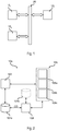
- Figure 1 shows a typical electronic system, such as the electronic system of a vehicle, comprising a plurality of processing systems 10, such as embedded systems or integrated circuits, e.g., a FPGA (Field Programmable Gate Array), DSP (Digital Signal Processor) or a micro-controller (e.g., dedicated to the automotive market).
- processing systems 10 such as embedded systems or integrated circuits, e.g., a FPGA (Field Programmable Gate Array), DSP (Digital Signal Processor) or a micro-controller (e.g., dedicated to the automotive market).
- FPGA Field Programmable Gate Array
- DSP Digital Signal Processor
- micro-controller e.g., dedicated to the automotive market.
- the communication system may include a vehicle control bus, such as a CAN (Controller Area Network) bus, and possibly a multimedia bus, such as a MOST (Media Oriented Systems Transport) bus, connected to vehicle control bus via a gateway.
- vehicle control bus such as a CAN (Controller Area Network) bus
- multimedia bus such as a MOST (Media Oriented Systems Transport) bus
- the processing systems 10 are located at different positions of the vehicle and may include, e.g., an Engine Control Unit (ECU), a Transmission Control Unit (TCU), an Anti-lock Braking System (ABS), a body control modules (BCM), and/or a navigation and/or multimedia audio system.
- ECU Engine Control Unit
- TCU Transmission Control Unit
- ABS Anti-lock Braking System
- BCM body control modules
- Future generation of processing systems in particular micro-controllers dedicated to automotive applications, will exhibit a significant increase in complexity, mainly due to the increasing number of functionalities (such as new protocols, new features, etc.) and to the tight constraints concerning the operation conditions of the system (such as lower power consumption, increased calculation power and speed, etc.).
- complexity is expected to increase in particular in the context of the forthcoming Car2X and autonomous driving world, because safety and security of the processing systems 10 will become more and more relevant.
- safety is intended to guarantee the functionality in case of both random and systematic faults, e.g., due to the corruption of "functional-critical" configuration data programmed during the production of the micro-controller, such as calibration data or other types of configuration data used to trim and/or configure the device functionalities.
- "functional-critical" configuration data programmed during the production of the micro-controller, such as calibration data or other types of configuration data used to trim and/or configure the device functionalities.
- calibration data or other types of configuration data used to trim and/or configure the device functionalities.
- ISO 26262 dictates a complete process and the requirements to achieve a functionality being compliant within the chosen safety goals.
- security is intended to guarantee the protection of the internal resources against malicious attacks, which, for example, might lead to the corruption of the above mentioned data.
- encryption of the communications between the various systems will become mandatory for the upcoming Car2X and autonomous driving scenario.
- safety and security should be treated in conjunction. For example, this becomes evident when considering a possible abnormal behavior of a processing system 10 of the vehicle. From a safety point of view, the micro-controller should still be able to operate permitting an operation of the vehicle, even in a "degraded" mode. Conversely, from security point of view, it might be advisable to stop the car, e.g., because the car might have been hacked. Unfortunately, the distinction of malfunctions or security faults may often not be taken, e.g., because often it is rather difficult to determine the actual failure root.
- the present application relates thus to a processing system according to the preamble of Claim 1, which is known, e.g. from document WO 2014/125326 A1 .
- Documents US 2016/146888 A1 , GB 2 255 212 A , US 2004/025086 A1 , US 2004/139443 A1 and US 9 495 239 B1 may also be of interest for the present invention.
- one or more of the above objectives is achieved by means of a processing system having the features specifically set forth in the claims that follow.
- Embodiments moreover concern a related integrated circuit, device and method.
- the processing system comprises at least one hardware block configured to change operation as a function of configuration data, a non-volatile memory comprising the configuration data for the at least one hardware block, and configuration means configured to read the configuration data from the non-volatile memory and provide the configuration data read from the non-volatile memory to the at least one hardware block.
- the processing system may comprise a processing unit, such as a microprocessor, and the configuration data may be stored in the non-volatile program memory for storing the firmware of the processing unit.
- the configuration means are configured to receive mode configuration data, read the configuration data from the non-volatile memory and test whether the configuration data contain errors by verifying whether the configuration data are corrupted and/or invalid.
- the configuration means may activate a normal operation mode of the processing system by providing the configuration data read from the non-volatile memory to the at least one hardware block.
- the configuration means may activate an error operation mode of the processing system as a function of the mode configuration data.
- the configuration means may provide reset values to the at least one hardware block when the mode configuration data indicate that a reset mode should be activated, and provide preset configuration data to the at least one hardware block when the mode configuration data indicate that a degraded mode should be activated.
- the configuration means may also activate a diagnostic module of the processing system when the mode configuration data indicate that a diagnostic mode should be activated.
- the configuration means comprise at least one configuration data client comprising a register for storing configuration data, wherein the configuration data stored in the register are provided to at least one hardware block.
- the configuration means may also comprise a configuration module.
- the configuration module may comprise a hardware data read module configured to read the configuration data from the non-volatile memory and a hardware dispatch module configured to send the configuration data read from the non-volatile memory to the at least one configuration data client.
- each configuration data client may have associated a respective address, and the hardware dispatch module may send the configuration data to the configuration data clients in the form of data packets addressed to a given configuration data client.
- the configuration module comprises also a hardware error and diagnostic module configured to test whether the configuration data contain errors by verifying whether the configuration data are corrupted and/or invalid, and in case the configuration data do contain errors, the error and diagnostic module may activate an error operation mode of the processing system as a function of the mode configuration data.
- the error and diagnostic module may:
- one or more of the configuration data clients may be configured to:
- the mode configuration data are stored in the non-volatile memory comprising also the configuration data.
- the configuration module may have associated a configuration data client, i.e., the configuration module may read via the data read module the mode configuration data from the non-volatile memory and send the mode configuration data via the dispatch module to the configuration data client associated with the configuration module.
- the error and diagnostic module may receive the mode configuration data from the configuration data client associated with the configuration module.
- the configuration means may also activate the error operation mode of the processing system as a function of additional life cycle data.
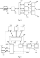
- Figure 2 shows a block diagram of an embodiment of a digital processing system 10a, such as a micro-controller.
- the processing system 10a comprises at least one processing unit 102, such as a microprocessor, usually the Central Processing Unit (CPU), programmed via software instructions.
- a processing unit 102 such as a microprocessor, usually the Central Processing Unit (CPU), programmed via software instructions.
- the software executed by the processing unit 102 is stored in a program memory 104a, such as a non-volatile memory, such as a Flash memory or EEPROM.
- the memory 104a may be integrated with the processing unit 102 in a single integrated circuit, or the memory 104a may be in the form of a separate integrated circuit and connected to the processing unit 102, e.g. via the traces of a printed circuit board.
- the memory 104a contains the firmware for the processing unit 102, wherein the term firmware includes both the software of a micro-processor and the programming data of a programmable logic circuits, such as a FPGA.
- the processing unit 102 may have associated one or more resources 106, such as:
- the digital processing systems 10a may support different functionalities.
- the processing systems may have different hardware architectures.
- the processing units 102 may have different architectures and processing speeds, and/or the number and type of the hardware resources 106 may vary.
- the behavior of the processing unit 102 is determined by the firmware stored in the memory 104a, e.g., the software instructions to be executed by a microprocessor 102 of a micro-controller 10a.
- the firmware stored in the memory 104a, e.g., the software instructions to be executed by a microprocessor 102 of a micro-controller 10a.
- the behavior of the processing system 10a may also be varied based on configuration data written, e.g. during the production stage.
- these configuration data may be written into specific areas of the non-volatile memory 104a and retrieved when the processing system 10a is powered on.
- the configuration data may be stored in an additional non-volatile memory 104b, such as a one-time programmable (OTP) memory, e.g. implemented with fuses.
- OTP one-time programmable
- the program memory 104a may be used, in case the blocks shown in Figure 2 are integrated in a common integrated circuit.
- an additional memory 104b may be used, in case the program memory 104a is an external memory, and only the other blocks are integrated in a common integrated circuit.
- the configuration data CD are stored in a non-volatile memory (104a and/or 104b) of the integrated circuit comprising the block requiring configuration data, such as the processing unit 102 and/or one or more of the hardware resources 106.
- configuration data CD are often calibration data used to guarantee that the hardware behavior is uniform, thereby compensating possible production process tolerances.
- this applies often to the calibration of analog components of the processing system, such as a temperature sensor, analog-to-digital converter, voltage reference, etc.
- a voltage monitor threshold level of an analog comparator could be "trimmed" to the exact intended value by adjusting some levels with configuration/calibration data, which are written by the producer of the hardware of the processing systems, e.g. the micro-controller producer.
- the configuration data CD may also be used to customize the behavior of the hardware, e.g., the hardware resources 106, according to different application needs. For example, once the firmware of the processing system has been stored in the processing system 10a, some configuration data may be written in order to deactivate the debug interface, which e.g. could be used to download the firmware of the processing system.
- a first part of the configuration data CD may be written by the producer of the hardware of the processing system (e.g., the producer of an integrated circuit), and/or a second part of the configuration data CD may be written by the developer of the firmware of the processing system 10a.
- the programmed configuration data CD may be read during a reset phase, which usually starts as soon as the processing system 10a is powered on.
- the processing system 10a may comprise for this purpose a configuration module 108 configured to read the configuration data CD from the non-volatile memory 104a and/or 104b, and distribute these configuration data CD within the processing system 10a.
- a configuration module 108 configured to read the configuration data CD from the non-volatile memory 104a and/or 104b, and distribute these configuration data CD within the processing system 10a.
- Figure 3 shows a possible embodiment for distributing the configuration data in the processing system 10a of Figure 2 .
- one or more configuration data CD are stored in one or more non-volatile memories 104 (i.e., memories 104a and/or 104b). In various embodiments, these configuration data CD are stored in reserved memory areas, e.g. in the form of a plurality of consecutive memory locations.
- the configuration module 108 accesses the reserved memory areas containing the configuration data CD, reads the configuration data CD and transmits the configuration data CD to a respective block 110 within the processing system 10a.
- the block 110 may corresponds to any block of the processing system 10a requiring configuration data and may correspond to the processing unit 102, a hardware resource 106, or even a memory (e.g. the memory 104a).
- the block 110 may be a power management controller of the processing system 10a, which may be configured to receive some calibration data for the internal voltage level trimming, and/or the various IPs, such as the hardware resources 106, whose behavior can be tailored by the customer according to their needs.
- each block 110 may have associated a respective configuration data client 112.
- each configuration data client 112 may be associated univocally to a single hardware block 110, and provided configuration data only to the associated hardware block 110, e.g. a specific hardware resource 106, or may be associated with a plurality of hardware blocks 110, e.g. a plurality of hardware resource 106.
- the configuration data clients 112a, 112b and 112c may also be integrated in the respective block 110a, 110b and 110c.
- the configuration module 108 may determine the respective configuration data (selected from the configuration data CD) for each target block 110 to be configured and transmit the configuration data associated with the target block to the configuration data client 112 associated with the target block 110. Similarly, while reading the configuration data CD from the memory 104, the configuration module 108 may determine the target block(s) for the current configuration information and send the current configuration data to the configuration data client(s) associated with the respective target block(s). Generally, any communication may be used for transmitting the configuration data to the configuration data client 112, including both serial and parallel communications. For example, the configuration module 108 and the configuration data clients 112 may be connected via a bus 114, and each configuration data clients 112 may have associated a respective target address.
- each configuration data client 112 is configured to receive the configuration data from the module 108, store them into the internal register, e.g. store them into one or more internal flip-flops or latches.
- the data stored in the register may then be used to generate one or more signals which influence the behavior of one or more hardware blocks 110.
- the register may comprise a bit providing a flag specifying whether a certain protection (e.g. the possibility to write a certain area of the non-volatile memory) over some internal assets shall be applied or not, wherein this flag is provided to the hardware block in charge of enforcing this protection.
- the module 108 distributes the configuration data CD preferably during the reset phase.
- the processing system 10a may be kept in the reset phase.
- the reset phase is usually considered both a safe and secured state, e.g., because when the processing system 10a (in particular the processing unit 102 and possibly the resources 106) is under reset, it usually cannot make damage to system it belongs to and it cannot be attacked as well.
- availability and testability of the processing system 10a may not be ensured.
- availability might be an issue, especially for the Car2X and autonomous driving world, where the system should be ready to react to its inputs, i.e., the run-time functionalities provided by the processing system 10a should be available.
- testability is almost impossible when the processing system 10a is kept under reset, e.g., upon a failure, i.e. the processing system 10a is unable to make a diagnosis of possible malfunctions.
- the processing system 10a described with respect to Figures 2 and 3 is thus modified in order to permit, even in case of malfunction, safety, security, availability, and testability of the processing system 10a.
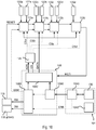
- FIG. 4 shows in this regard a second embodiment of a processing system 10a in accordance with the present invention.
- the processing system 10a comprises a configuration module 108 configured to read the configuration data CD form one or more non-volatile memories 104 (e.g ., memories 104a and/or 104b, and a plurality of configuration data clients 112 configured to receive respective configuration data from the module 108 and distribute them among a plurality of blocks 110 (not shown) requiring configuration data.
- each configuration data client 112 may be associate univocally with a respective block 110.
- the processing system 10a comprises again three configuration data clients 112a, 112b and 112c.
- the configuration module 108 comprises a data read module 1080 configured to read the configuration data CD from the memory 104 and a dispatch module 1082 configured to transmit the configuration data to the configuration data clients 112.
- any communication may be used for communication between the dispatch module 1082 and the configuration data clients 112.
- the communication between the dispatch module 1082 and the configuration data clients 112 is based on a data frames in accordance with a given format, called in the following Device Configuration Format (DCF).
- DCF Device Configuration Format
- each data frame comprises two fields: the payload (i.e., the real data), called DCF Format payload, and possible additional data attributes used to identify the receiver of the data, called DCF Format attributes, wherein the receiver is one of the configuration data clients 112 representing a DCF client.
- the data attributes may consist in 16 or 32 bits, wherein a given number of bits specifies the address of one of the configuration data clients 112, and the payload may consist in 16 or 32 bits.
- the data read module 1080 is configured to read blocks of 64 bits from the memory 104, wherein the first 32 bits contain the data attributes (including the address of a configuration data client) and the second 32 bits contain the configuration data to be transmitted to the address specified in the data attributes.
- each configuration data client/DCF client 112 may be a hardware module, usually comprising a combinational circuit configured to store the received data in an internal register implemented, e.g., with flip-flops/latches, thereby permitting to distribute, via one or more internal signals generated as a function of the data stored in the internal register, the configuration data received to various parts of the associate hardware block(s) 110.
- each configuration data client 112 may have associated a univocal address (i.e., univocal within each processing system 10a) and analyse the data transmitted by the dispatch module 1082 in order to determine whether the additional data attributes (DCF Format attributes) contain the address associated with the configuration data client 112.
- the module 108 comprises an error and diagnostic module 1084 configured to manage the various modes of operation of the processing system 10a.
- corrupted data may be detected by storing one of more additional check bits together with the configuration data CD in the memory 104.
- these additional bits may be analyzed and compared with the configuration data read directly by a memory interface 1040 of the memory 104, or by the error and diagnostic module 1084.
- the memory interface 1040 of the memory 104 may be used, in case the memory contains additional check bits for all data stored in the non-volatile memory 104, i.e., the memory may be a memory with ECC (Error-Correcting Code).
- ECC Error-Correcting Code
- the memory interface 1040 may generate an error signal ERR when the data read from the memory 104 are corrupted.
- the error and diagnostic module 1084 may analyze the configuration data CD and the additional check bits, in case the additional check bits are stored only for the configuration data CD, e.g. when the additional check bits are stored in the data attributes field.
- the error and diagnostic module 1084 may analyze the configuration data CD read from the memory 104 in order to determine invalid configuration data.
- each configuration data client 112 may also verify the configuration data received and determine whether the respective configuration data are valid. In this case, each configuration data client 112 may signal an error to the error and diagnostic module 1084 indicating that the received configuration data are invalid.
- the error and diagnostic module 1084 may generate a reset mode signal RM for the reset module 116 of the processing system 10a in order to activate the reset state.
- this step is purely optional, because the reset module 116 could also activate automatically the reset state.
- the specific implementation of the reset module 116 depends on architecture of the processing system. For example, the reset module 116 may generate a reset pulse of a given number of clock cycles provided to the blocks 110 of the processing system 10a.
- the data read module 1080 may read the configuration data CD from the memory 104 and the error and diagnostic module 1084 may determine (directly or indirectly via the memory interface 1040 of the memory 104) whether the configuration data CD are corrupted. In various embodiments, the error and diagnostic module 1084 may also determine whether the configuration data are valid.
- the error and diagnostic module 1084 may send a signal to the dispatch module 1082 and the dispatch module 1082 may distribute the configuration data CD.
- the configuration data CD may be verified and distributed sequentially, or the complete configuration data CD may be read and verified before these data are indeed transmitted to the various configuration data clients 112.
- the dispatch module 1082 will distribute the configuration data CD, thereby activating the processing system 10a, i.e., the various blocks 110 will use the configuration data CD stored in the memory 104 (normal operation mode).
- the error and diagnostic module 1084 may perform different tasks.
- the error and diagnostic module 1084 may drive the reset module 112 of the processing system 10a via the signal RM, in order to perform a new reset of the processing system 10a.
- the processing system 10a is kept in a reset mode when the configuration data are permanently corrupted or invalid.
- the processing system 10a may however support also further operation modes, such as a safe secure mode and/or a diagnostic mode.
- the error and diagnostic module 1084 may activate the safe security mode by providing via the dispatch module 1082 a set of preset configuration data to the configuration data clients.
- the preset configuration data may also be stored directly within each configuration data client 112 and the error and diagnostic module 1084 may inform the configuration data clients 112, e.g., via a safe secure mode signal SSM, that the preset configuration data should be used.
- these preset configuration data correspond to configuration data for operating the various blocks 110 in an ISO 26262 "degraded" mode, wherein preferably additional security features are activated. Accordingly, once each configuration data client 112 has stored the preset configuration data in the internal register, the processing system 10a is started and the various blocks 110 will use the preset configuration data.
- the error and diagnostic module 1084 may activate the diagnostic mode by activating via a diagnostic mode signal DM a diagnostic module 118, so called design for testability (DFT), of the processing system 10a.
- DFT design for testability
- the diagnostic module 118 depends on the architecture of the processing system.
- the diagnostic block 118 may be configured to instruct the various blocks 110 of the processing system 10a to perform a given sequence of tasks, thereby executing a predefines test cycle. For example, during the test cycle, the blocks 110 may be instructed to generate given output signals at the pins of the processing system 10a.
- the error and diagnostic module 1084 may activate one of the following error states:
- the above modes of operation are not mutually exclusive, but as will be described in the following, different combinations of them are possible by providing appropriate preset configuration information to the various blocks 110, and activating or deactivating the reset module 116 and the diagnostic module 118.
- some blocks 110 may use the configuration data stored in the memory 104, while the blocks 110 with corrupted/invalid configuration data may use the preset configuration data.
- FIG. 5 shows a possible embodiment of the above operations.
- the complete management of the operation modes of the processing system 10a is again managed by the error and diagnostic module 1084, representing thus a mode selection circuit.
- the configuration data CD are stored in the non-volatile memory 104, which is configure to determine whether the configuration data are corrupted.
- the memory 104 comprises a memory interface 1040 configured to determine, e.g., based on additional ECC bits stored in the memory 104, a signal ERR indicating whether the configuration data CD are corrupted.
- the data read module 1080 is configured to read the configuration data CD from the memory 104 and the memory 104 signals also whether the data read are corrupted, e.g. via the signal ERR transmitted to the module 1084.
- the dispatch module 1082 provides the configuration data read from the memory to the various configuration data clients 112.
- the dispatch module 1082 may generate a data signal DATA having a given number of bits (corresponding to the bits of the payload) containing the configuration data to be transmitted to a given configuration data client 112 and further control signals for selecting the target configuration data client (i.e. the additional data attributes).
- the dispatch module 1082 generates also an address signal ADR containing the address of the target configuration data client 112 and optionally a chip select signal CS used to signal to the configuration data clients 112 that the address signal ADD and the data signal DATA are valid.
- the address signal ADR (and the chip select signal CS) may be provided to a decoder 124 configured to activate one of the configuration data clients 112 as a function of the address signal ADD.
- the decoder 124 may set a chip select signal CSa in order to indicate that the configuration data client 112a should read the data signal DATA when the address signal ADD corresponds to an address assigned to the configuration data client 112a (and the chip select signal CS is set).
- the decoder 124 may set a chip select signal CSb in order to indicate that the configuration data client 112b should read the data signal DATA when the address signal ADR corresponds to an address assigned to the configuration data client 112b (and the chip select signal CS is set), etc.
- each configuration data client 112 may receive at input various data signals, selected as a function of a reset signal RESET generate by the reset module 112 and the safe security mode SSM signal generated by the module 108, in particular the error and diagnostic module 1084:
- Figure 7 shows a possible embodiment of the configuration data client 112a which may be used in the embodiment shown in Figure 6 .
- the same architecture may also be used for the other configuration data client.
- the configuration data client 120a has associated reset data 120a and preset configuration data 122.
- these data are hardwired within the configuration data client 120a.
- the configuration data client 120a receives at input the configuration data DATA from the dispatch module.
- the configuration data client 120a is configured to store one of these data (reset, preset configuration data or received configuration data) in an internal register 1120 as a function of the chip select signal CSa, the safe secure mode signal SSM and the reset signal RESET.
- the configuration data client 120a comprises:
- the reset data 120a when the reset signal RESET is set, the reset data 120a will be stored in the register 1120. Conversely, when the reset signal is not set and the safe secure mode signal SSM is set, the preset configuration data 122a will be stored in the register 1120. Conversely, if both signal are not set, the chip select signal CSa determines whether the data DATA or the previous configuration data CDa should be stored in the register 1120.
- the switching between the various operation states of the processing system 10a is managed by the error and diagnostic module 1084.
- the module 1084 may support the following modes:
- the module 1084 activates the reset mode when the processing system 10a is switched on. During this mode, the module 1084 drives the reset module 116, which thus generates the reset signal RESET and the various configuration data clients load the reset data into the internal register.
- the module 108 reads via the data read module 1080 the configuration data CD from the non-volatile memory 104 and transmits the configuration data read to the various configuration data clients 112, thereby overwriting the reset data.
- the error and diagnostic module 1084 may enable the safe secure mode and/or the diagnostic mode.
- the error and diagnostic module 1084 may activate the safe secure mode by setting the signal SSM, whereby the configuration data clients 112 read the respective preset configuration data 122.
- the error and diagnostic module 1084 may activate the diagnostic mode by sending a signal DM to the diagnostic module 118.
- This diagnostic module 114 may then activate diagnostic functions in the various blocks 110.
- the memory 104 may comprise a test logic 1042 configured to verify the non-volatile memory 104 and a signal DIAG generated by the diagnostic module 118 or directly the signal DM may be used to activate this test logic 1042.
- the error and diagnostic module 1084 requires some additional information in order to decide whether the safe secure mode and/or the diagnostic mode should be activated.
- this information representing mode configuration data MCD, may be stored in a non-volatile memory, such as a one-time programmable memory, associated with the module 108. Conversely, in other embodiments, this information is stored in the non-volatile memory 104.
- the mode configuration data are encoded with plurality of bits, wherein:
- a single keyword/bit sequence may be used for all blocks 110, i.e. the error and diagnostic module 1084 is configured to activate the safe secure mode and/or the diagnostic mode for all blocks 110.
- a respective keyword/bit sequence may be stored for each block 110, i.e. the error and diagnostic module 1084 is configured to selectively activate the safe secure mode and/or the diagnostic mode for each block 110.
- the memory 104 may provide the mode configuration data MCD consisting in a given number of bits, such as 32 bits, wherein a first subset of the bits, e.g., the bits [31:16], are associated with the diagnostic mode, and a second subset of the bits, e.g., the bits [15:0], are associated with the safe secure mode.
- the module 1084 may activate the diagnostic mode by setting the signal DIAG, and when the second subset of bits corresponds to a given reference bit sequence, e.g., 0x5E5A, the module 1084 may activate the safe secure mode by setting the signal SSM.
- the module 1084 may activate the reset mode via the reset module 116. Accordingly, in the embodiment considered, the reset mode is also activated when bits of the mode configuration data MCD are corrupted.
- the use of a plurality of bits for the first and second subset of bits ensures that a single bit error of these mode configuration data MCD may not activate incidentally the diagnostic mode or the safe secure mode, but at most the reset state is activated.
- the mode configuration data MCD may be stored directly in the non-volatile memory 104, i.e., the memory in which are also stored the configuration data CD.
- the mode configuration data are stored at one or more fixed memory locations of the non-volatile memory or together with the configuration data.
- Figure 9 shows an embodiment, in which the mode configuration data MCD are stored at one or more fixed memory locations.
- the module 108 may read the mode configuration data MCD via the data read module 1080 and store them in an internal register 1086.
- the module 1084 may compare the mode configuration data MCD stored in the internal register 1086 with the respective reference bit sequences in order to decide which error more (reset, diagnostic or safe secure mode) should be activated.
- the module 108 may extract the mode configuration data and store them in the internal register 1086.
- Figure 10 shows an embodiment, in which an additional configuration data client 112d is used.
- the configuration data client 112d is configured to store in an internal register during a reset state a given reset value 120d and overwrite the reset values by storing the data received from the module 108.
- the configuration data client 112d may have associated a respective address ADR.
- the decoder 124 may generate a chip select signal CSd when the address ADR provided by the module 108 corresponds to the address associated with the configuration data client 112d.
- the configuration data client 112d does not have associated preset values 122d. For this reason, the multiplexer 1124 in Figure 7 may also be omitted.
- the architecture of the other configuration data clients 112 may be used, by simply setting the respective preset configuration data 122 to the reset values 120.
- the configuration module 108 in particular the dispatch module 1082, distributes the configuration data CD read from the memory 104 to the various configuration data clients 112, without knowing that these data include also the mode configuration data MCD.
- the configuration data client 112d represents thus the configuration data client associated with the configuration module 108, wherein the configuration data client 112d provides the mode configuration data MCD the configuration module 108, in particular the error and diagnostic module 1084.
- the module 108 passes the mode configuration data read from the memory 104 to the configuration data client 112d and receives from the same the stored configuration data, i.e., the mode configuration data MCD.
- the memory interface 1042 may report via the signal ERR a data error to the module 108 and the error and diagnostic module 1084 may determine the reaction of the processing systems 10a by means of the signals SSM, DM and RM.
- the module 1082 may trigger a new reset by driving the reset module 112 via the signal RM. Accordingly, the processing system 10a (including the blocks 110 and the also the configuration module 108) will perform a new restart. The configuration data clients 112 will thus re-load the default reset values 120 (which is fixed at design time) in response to the reset signal RESET generate by the reset module 116. Next, the configuration module 108 will perform a new attempt to read the configuration data CD from the non-volatile memory 104. Accordingly, in case the configuration data are permanently corrupted, the processing system 10a may be kept in the reset mode by performing an infinite number of reset loops. Generally, the configuration module 108 may also monitor the number of resets performed and interrupt the reset loop.
- the mode configuration data MCD may indicate that the preset configuration data 122 should be used.
- this mode may only be activated once the configuration module 108 has read the mode configuration data MCD from the memory 104 (and possibly transmitted to the configuration data client 112d).
- the error and diagnostic module 1084 Once activated, the error and diagnostic module 1084 generates the signal SSM, and the configuration data clients 112 associated with the blocks 110 (in particular the clients 112a-112c) will load the preset configuration data 122.
- the configuration data client 112d associated with the module 108 may not have associates preset configuration data 122.
- the preset configuration data 122 may be fixed during the design of the processing system 10a, e.g., hardwired. As mentioned before, each block 110 should be designed that in response to the preset configuration data 122, the block 110 should still be able to operate, possibly with reduced device functionality. Accordingly, once the signal SSM is set, the configuration data clients 112a-112c will replace the reset data 120 (or already loaded configuration data) with the preset configuration data 122.
- the error and diagnostic module 1084 may generate the signal DM in order to activate the diagnostic module 118, which e.g. performs one or more system tests.
- this mode may only be activated once the configuration module 108 has read the mode configuration data MCD from the memory 104 (and possibly transmitted to the configuration data client 112d). For example, once activated, several internal signals might be exposed on some internal non-bonded pads. Another possibility is that the non-volatile memory 104 might enable some test features on some areas of the memory that usually cannot be analyzed for security reason.
- configuration data may relate to security aspects, such as a cipher key to be used by a hardware secure element.
- security related configuration data are usually stored in separate memory locations or a separate non-volatile memory.
- these security related configuration data are stored in encrypted format and the memory interface may be configured to decrypt these data.
- each block 110 may have associated two or more independent configuration data clients 112, e.g., one for the non-security related configuration data and another for the security related configuration data.
- the above modes may thus be activated by writing the mode configuration data into the memory 104.
- at least the diagnostic mode may provide sensible data from a security point of reason, e.g. because the memory interface 1040 could perform a sequential readout of the data stored in the memory 104 and make the data available via one or more pads of the processing system 10a.
- Figure 11 shows in this regard an embodiment, in which the configuration module 108 is configured to take into account also the life cycle of the processing system.
- this life cycle may be encoded with a bit sequence.
- this bit sequence is stored in a non-volatile memory 126, preferably a one-time programmable memory.
- this life cycle data LCD may also be stored at reserved memory locations of the memory 104.
- bit sequence LCD stored in the memory 122 may indicate one of the following stages:
- the error and diagnostic module 1084 may not only take into account the mode configuration data MCD but also the product life cycle as indicated by the bit sequence LCD stored in the memory 126.
- the configuration module 108 may distribute the configuration data CD to the configuration data clients 112 and the processing system 10a is normally operated with these configuration data, i.e. the mode configuration data MCD and the product life cycle data LCD are not taken into account at all.
- the configuration module 108 uses these data only when the configuration data CD are corrupted (or invalid).
- the configuration module 108 may use the mode configuration data MCD, which may indicate that any of the previous modes may be activated (i.e., reset, diagnostic, safe secure or both diagnostic and safe secure).
- the reset mode corresponds to the default mode, which is used, e.g., in case the mode configuration data are corrupted (or invalid)
- the configuration module 108 may disregard the mode configuration data MCD and the reset mode may be used by default.
- the module 108 may only permit an activation of the safe secure mode as an alternative to the default reset mode, i.e. the configuration module 108 may activate the safe secure mode only when the mode configuration data MCD indicate that the safe secure mode should be used.
- the diagnostic mode can only be activated by the producer of the processing system 10a, but cannot be activated, e.g., when the processing system 10a is indeed used ("in field" stage).
- this mode corresponds in general to a downgraded mode, in which preset configuration data are used.
- the preset configuration data may activate also these security related features.
Landscapes
- Engineering & Computer Science (AREA)
- Theoretical Computer Science (AREA)
- General Engineering & Computer Science (AREA)
- Quality & Reliability (AREA)
- Physics & Mathematics (AREA)
- General Physics & Mathematics (AREA)
- Health & Medical Sciences (AREA)
- Biomedical Technology (AREA)
- Computer Hardware Design (AREA)
- Techniques For Improving Reliability Of Storages (AREA)
- Automation & Control Theory (AREA)
- Human Computer Interaction (AREA)
- Transportation (AREA)
- Mechanical Engineering (AREA)
Claims (11)
- Verarbeitungssystem (10a), das Folgendes umfasst:- mindestens einen Hardware-Block (110), der konfiguriert ist, den Betrieb als Funktion von Konfigurationsdaten (CD) zu ändern;- einen nichtflüchtigen Speicher (104), der die Konfigurationsdaten (CD) für den mindestens einen Hardware-Block (110) enthält; und- Konfigurationsmittel (108, 112), die konfiguriert sind, die Konfigurationsdaten (CD) aus dem nichtflüchtigen Speicher (104) zu lesen und die Konfigurationsdaten (CD), die aus dem nichtflüchtigen Speicher (104) gelesen wurden, zu dem mindestens einen Hardware-Block (110) zu liefern;dadurch gekennzeichnet, dass die Konfigurationsmittel (108, 112) Folgendes umfassen:- mehrere Konfigurationsdaten-Clients (112a-112c), wobei jeder Konfigurationsdaten-Client (112a-112c) ein Register (1120) zum Speichern von Konfigurationsdaten umfasst, die Konfigurationsdaten, die in den Registern (1120) gespeichert sind, dem mindestens einen Hardware-Block (110) geliefert werden und jedem Konfigurationsdaten-Client (112a-112c) eine entsprechende Adresse zugeordnet ist; und- ein Konfigurationsmodul (108), das konfiguriert ist, Moduskonfigurationsdaten (MCD) zu empfangen, und Folgendes umfasst:a) ein Hardware-Daten-Lesemodul (1080), das konfiguriert ist, die Konfigurationsdaten (CD) aus dem nichtflüchtigen Speicher (104) zu lesen, wobei die Konfigurationsdaten (CD) im nichtflüchtigen Speicher (104) gespeichert sind und in Form von Datenrahmen, die ein Attributfeld, das die Adresse eines Zielkonfigurationsdaten-Clients (112) umfasst, und als Nutzlast die entsprechenden Konfigurationsdaten umfassen, kommuniziert werden;b) ein Hardware-Auslieferungsmodul (1082), das konfiguriert ist, die Konfigurationsdaten (CD), die aus dem nichtflüchtigen Speicher (104) gelesen wurden, in Form von Datenpaketen, die an einen gegebenen Konfigurationsdaten-Client (112a-112c) der mehreren Konfigurationsdaten-Clients (112a-112c) adressiert sind, zu den mehreren Konfigurationsdaten-Clients (112a-112c) zu senden; undc) ein Hardware-Fehler- und Diagnosemodul (1084), das konfiguriert ist zum- Prüfen, ob die Konfigurationsdaten (CD) Fehler enthalten, indem geprüft wird, ob die Konfigurationsdaten (CD), die aus dem nichtflüchtigen Speicher (104) gelesen worden sind, beschädigt und/oder ungültig sind,- falls die Konfigurationsdaten (CD) keine Fehler enthalten, Aktivieren eines normalen Betriebsmodus des Verarbeitungssystems (10a) durch Liefern der Konfigurationsdaten (CD), die aus dem nichtflüchtigen Speicher (104) gelesen wurden, zum mindestens einen Hardware-Block (110) und- falls die Konfigurationsdaten (CD) Fehler enthalten, Aktivieren eines Fehlerbetriebsmodus des Verarbeitungssystems (10a) als Funktion der Moduskonfigurationsdaten (MCD) durch- Ansteuern eines Rücksetzmoduls (112) des Verarbeitungssystems (10a), um ein neues Zurücksetzen des Verarbeitungssystems (10a) durchzuführen, wenn die Moduskonfigurationsdaten (MCD) anzeigen, dass ein Rücksetzmodus aktiviert werden soll, wodurch Rücksetzwerte (120) zum mindestens einen Hardware-Block (110) geliefert werden, wenn die Moduskonfigurationsdaten (MCD) anzeigen, dass ein Rücksetzmodus aktiviert werden soll, und- Liefern voreingestellter Konfigurationsdaten (122) zum mindestens einen Hardware-Block (110), wenn die Moduskonfigurationsdaten (MCD) anzeigen, dass ein herabgestufter Modus aktiviert werden soll; wobeidie Moduskonfigurationsdaten (MCD) gemeinsam mit den Konfigurationsdaten (CD) im nichtflüchtigen Speicher (104) gespeichert werden und dem Konfigurationsmodul (108) ein Konfigurationsdaten-Client (112d) zugeordnet ist, wobei das Konfigurationsmodul (108)- die Moduskonfigurationsdaten (MCD) aus dem nichtflüchtigen Speicher (104) liest,- die Moduskonfigurationsdaten (MCD), die aus dem nichtflüchtigen Speicher (104) gelesen wurden zum Konfigurationsdaten-Client (112d), der dem Konfigurationsmodul (108) zugeordnet ist, sendet und- die Moduskonfigurationsdaten (MCD) vom Konfigurationsdaten-Client (112d), der dem Konfigurationsmodul (108) zugeordnet ist, empfängt.
- Verarbeitungssystem (10a) nach Anspruch 1, wobei die Konfigurationsmittel (108, 112) konfiguriert sind,- dann, wenn die Konfigurationsdaten (CD) Fehler enthalten, ein Diagnosemodul (118) des Verarbeitungssystems (10a) zu aktivieren, wenn die Moduskonfigurationsdaten (MDU) anzeigen, dass ein Diagnosemodus aktiviert werden soll.
- Verarbeitungssystem (10a) nach Anspruch 2, wobei die Moduskonfigurationsdaten (MCD) aus einer gegebenen Anzahl Bits bestehen, eine erste Untermenge der Bits der Moduskonfigurationsdaten (MCD) dem Diagnosemodus zugeordnet ist, eine zweite Untermenge der Bits der Moduskonfigurationsdaten (MCD) dem herabgestuften Modus zugeordnet ist und das Hardware-Fehler- und Diagnosemodul (1084) konfiguriert ist,- dann, wenn die erste Untermenge Bits einer ersten gegebenen Bezugsbitfolge entspricht, das Diagnosemodul (118) zu aktivieren,- dann, wenn die zweite Untermenge Bits einer gegebenen zweiten Bezugsbitfolge entspricht, die voreingestellten Konfigurationsdaten (122) dem mindestens einen Hardware-Block (110) zu liefern und- dann, wenn weder die erste noch die zweite Untermenge Bits der ersten bzw. der zweiten Bitfolge entsprechen, das Rücksetzmodul (112) des Verarbeitungssystems (10a) anzusteuern, um ein erneutes Zurücksetzen des Verarbeitungssystems (10a) durchzuführen.
- Verarbeitungssystem (10a) nach einem der vorhergehenden Ansprüche, wobei das Hardware-Fehler- und Diagnosemodul (1084) konfiguriert ist,- ein Herabstufungsmodussignal (SSM) zu setzen, wenn die Moduskonfigurationsdaten (MCD) anzeigen, dass der herabgestufte Modus aktiviert werden soll; und- ein Rücksetzmodussignal (RM), das dem Rücksetzmodul (116) des Verarbeitungssystems (10a) geliefert wird, zu setzen, wenn die Moduskonfigurationsdaten (MCD) anzeigen, dass der Rücksetzmodus aktiviert werden soll, wobei das Rücksetzmodul (116) konfiguriert ist, ein Zurücksetzen (RESET) des Verarbeitungssystems (10a) als Funktion des Rücksetzmodussignals (RM) wahlweise durchzuführen.
- Verarbeitungssystem (10a) nach Anspruch 4, wobei der Konfigurationsdaten-Client (112a-112c) konfiguriert ist,- dann, wenn das Rücksetzmodul (116) anzeigt, dass ein Zurücksetzen (RESET) durchgeführt werden sollte, die Rücksetzwerte (120) im Register (1120) zu speichern;- dann, wenn das Herabstufungsmodussignal (SSM) gesetzt ist, die voreingestellten Konfigurationsdaten (122) im Register (1120) zu speichern und- dann, wenn das Rücksetzmodul (116) anzeigt, dass kein Zurücksetzen (RESET) durchgeführt werden sollte, und das Herabstufungsmodussignal (SSM) nicht gesetzt ist, die Konfigurationsdaten (CD), die vom Hardware-Auslieferungsmodul (1082) empfangen wurden, im Register (1129) zu speichern.
- Verarbeitungssystem (10a) nach einem der vorhergehenden Ansprüche, wobei der nichtflüchtige Speicher (104) eine Speicherschnittstelle (1040) umfasst, die konfiguriert ist, ein Fehlersignal (ERR) zu den Konfigurationsmitteln (108, 112) zu senden, wenn die Konfigurationsdaten (CD) beschädigt sind.
- Verarbeitungssystem (10a) nach einem der vorhergehenden Ansprüche, wobei die Konfigurationsmittel (108, 112) konfiguriert sind,- Lebenszyklusdaten (LCD) zu empfangen und- falls die Konfigurationsdaten (CD) Fehler enthalten, einen Fehlerbetriebsmodus des Verarbeitungssystems (10a) als Funktion der Lebenszyklusdaten (LCD) zu aktivieren.
- Verarbeitungssystem (10a) nach einem der vorhergehenden Ansprüche, wobei das Verarbeitungssystems (10a) Folgendes umfasst:- eine Verarbeitungseinheit (102) und- einen nichtflüchtigen Programmspeicher (104a) zum Speichern der Firmware der Verarbeitungseinheit (102), wobei die Konfigurationsdaten (CD) im nichtflüchtigen Programmspeicher (104a) gespeichert sind.
- Integrierte Schaltung, die ein Verarbeitungssystem (10a) nach einem der Ansprüche 1 bis 8 umfasst.
- Vorrichtung, die mehrere Verarbeitungssysteme (10a) nach einem der Ansprüche 1 bis 8 umfasst.
- Verfahren, das durch ein Verarbeitungssystem (10a) nach einem der Ansprüche 1 bis 8 durchgeführt wird und das die Schritte, die durch die Konfiguration des Verarbeitungssystems definiert sind, umfasst.
Applications Claiming Priority (1)
| Application Number | Priority Date | Filing Date | Title |
|---|---|---|---|
| IT102017000050166A IT201700050166A1 (it) | 2017-05-09 | 2017-05-09 | Sistema di elaborazione, relativo circuito integrato, dispositivo e procedimento |
Publications (2)
| Publication Number | Publication Date |
|---|---|
| EP3401183A1 EP3401183A1 (de) | 2018-11-14 |
| EP3401183B1 true EP3401183B1 (de) | 2020-04-22 |
Family
ID=59812014
Family Applications (1)
| Application Number | Title | Priority Date | Filing Date |
|---|---|---|---|
| EP18171268.8A Active EP3401183B1 (de) | 2017-05-09 | 2018-05-08 | Verarbeitungssystem, zugehörige integrierte schaltung, vorrichtung und verfahren |
Country Status (3)
| Country | Link |
|---|---|
| US (2) | US10754723B2 (de) |
| EP (1) | EP3401183B1 (de) |
| IT (1) | IT201700050166A1 (de) |
Cited By (1)
| Publication number | Priority date | Publication date | Assignee | Title |
|---|---|---|---|---|
| EP4078314A1 (de) * | 2019-12-20 | 2022-10-26 | Robert Bosch GmbH | Vorrichtung mit einer schnittstelle und verfahren zum betreiben einer vorrichtung mit einer schnittstelle |
Families Citing this family (6)
| Publication number | Priority date | Publication date | Assignee | Title |
|---|---|---|---|---|
| IT201800002895A1 (it) | 2018-02-21 | 2019-08-21 | Stmicroelectronics Application Gmbh | Sistema di elaborazione, relativo circuito integrato, dispositivo e procedimento |
| US10855529B2 (en) | 2018-11-26 | 2020-12-01 | Stmicroelectronics Application Gmbh | Processing system, related integrated circuit, device and method |
| JP2021111112A (ja) * | 2020-01-09 | 2021-08-02 | キヤノン株式会社 | 画像形成装置、及びその制御方法 |
| US12175808B2 (en) | 2021-04-27 | 2024-12-24 | Garrett Transportation I Inc. | Advanced control framework for automotive systems |
| IT202200002093A1 (it) | 2022-02-07 | 2023-08-07 | St Microelectronics Srl | Sistema di elaborazione, relativo circuito integrato e procedimento |
| DE102023127139A1 (de) * | 2023-10-05 | 2025-04-10 | Infineon Technologies Ag | System-on-chip mit sicherem hardware-subsystem |
Family Cites Families (19)
| Publication number | Priority date | Publication date | Assignee | Title |
|---|---|---|---|---|
| GB9108599D0 (en) * | 1991-04-22 | 1991-06-05 | Pilkington Micro Electronics | Peripheral controller |
| US7007203B2 (en) * | 2002-08-02 | 2006-02-28 | Motorola, Inc. | Error checking in a reconfigurable logic signal processor (RLSP) |
| US7058854B2 (en) * | 2002-08-27 | 2006-06-06 | Lsi Logic Corporation | Automode select |
| US20040139443A1 (en) * | 2003-01-13 | 2004-07-15 | Hatle Mark G. | Systems and methods for recreating configuration data |
| US7308610B2 (en) * | 2004-12-10 | 2007-12-11 | Intel Corporation | Method and apparatus for handling errors in a processing system |
| DE102006018831A1 (de) * | 2006-04-22 | 2007-10-25 | Daimlerchrysler Ag | Kraftfahrzeugdiagnose und Fahrzeugannahme |
| US7779305B2 (en) * | 2007-12-28 | 2010-08-17 | Intel Corporation | Method and system for recovery from an error in a computing device by transferring control from a virtual machine monitor to separate firmware instructions |
| DE102009030774B4 (de) * | 2009-06-27 | 2020-01-30 | Bayerische Motoren Werke Aktiengesellschaft | Verfahren zur rechnergestützten Erfassung von Fehlern beim Ablauf von einem oder mehreren softwarebasierten Programmen in einem System aus Komponenten |
| CN102081562A (zh) * | 2009-11-30 | 2011-06-01 | 华为技术有限公司 | 一种设备诊断方法及系统 |
| TW201417001A (zh) * | 2012-10-23 | 2014-05-01 | Hon Hai Prec Ind Co Ltd | 電子設備工作模式切換系統及方法 |
| WO2014125326A1 (en) * | 2013-02-12 | 2014-08-21 | Freescale Semiconductor, Inc. | Configuration controller for and a method of controlling a configuration of a circuitry |
| EP2989583B1 (de) * | 2013-04-23 | 2018-10-10 | Hewlett-Packard Development Company, L.P. | Konfigurieren eines systems |
| US9767264B2 (en) * | 2014-05-23 | 2017-09-19 | Ricoh Company, Ltd. | Apparatus, method for controlling apparatus, and program |
| US9495239B1 (en) * | 2014-08-22 | 2016-11-15 | Xilinx, Inc. | User-configurable error handling |
| JP6387756B2 (ja) * | 2014-09-11 | 2018-09-12 | 株式会社リコー | 機器、管理モジュール、プログラムおよび制御方法 |
| US9836373B2 (en) * | 2014-11-26 | 2017-12-05 | Texas Instruments Incorporated | On-chip field testing methods and apparatus |
| US10289871B2 (en) * | 2015-11-02 | 2019-05-14 | Nxp Usa, Inc. | Integrated circuit lifecycle security with redundant and overlapping crosschecks |
| US10198332B2 (en) * | 2016-10-07 | 2019-02-05 | Infineon Technologies Ag | System on chip integrity verification method and system |
| US10372545B2 (en) * | 2017-03-13 | 2019-08-06 | Infineon Technologies Ag | Safe reset techniques for microcontroller systems in safety related applications |
-
2017
- 2017-05-09 IT IT102017000050166A patent/IT201700050166A1/it unknown
-
2018
- 2018-05-08 EP EP18171268.8A patent/EP3401183B1/de active Active
- 2018-05-09 US US15/975,507 patent/US10754723B2/en active Active
-
2020
- 2020-07-14 US US16/928,768 patent/US11210161B2/en active Active
Non-Patent Citations (1)
| Title |
|---|
| None * |
Cited By (2)
| Publication number | Priority date | Publication date | Assignee | Title |
|---|---|---|---|---|
| EP4078314A1 (de) * | 2019-12-20 | 2022-10-26 | Robert Bosch GmbH | Vorrichtung mit einer schnittstelle und verfahren zum betreiben einer vorrichtung mit einer schnittstelle |
| EP4078314B1 (de) * | 2019-12-20 | 2026-03-04 | Robert Bosch GmbH | Vorrichtung mit einer schnittstelle und verfahren zum betreiben einer vorrichtung mit einer schnittstelle |
Also Published As
| Publication number | Publication date |
|---|---|
| IT201700050166A1 (it) | 2018-11-09 |
| US20180329774A1 (en) | 2018-11-15 |
| US11210161B2 (en) | 2021-12-28 |
| US20200341836A1 (en) | 2020-10-29 |
| US10754723B2 (en) | 2020-08-25 |
| EP3401183A1 (de) | 2018-11-14 |
Similar Documents
| Publication | Publication Date | Title |
|---|---|---|
| EP3401183B1 (de) | Verarbeitungssystem, zugehörige integrierte schaltung, vorrichtung und verfahren | |
| US11474752B2 (en) | Processing system including one-time programmable memory with original life cycle data, related integrated circuit, device and method | |
| EP3413195B1 (de) | Verarbeitungssystem, zugehörige integrierte schaltung, vorrichtung und verfahren | |
| EP3719636B1 (de) | Verarbeitungssystem, zugehörige integrierte schaltung, vorrichtung und verfahren | |
| EP4068101A1 (de) | Verarbeitungssystem, zugehörige integrierte schaltung, vorrichtung und verfahren | |
| US11822934B2 (en) | Processing system, related integrated circuit, device and method | |
| EP3657345B1 (de) | Verarbeitungssystem, zugehörige integrierte schaltung, vorrichtung und verfahren | |
| US10845999B2 (en) | Processing system, related integrated circuit, device and method | |
| EP4064100B1 (de) | Verarbeitungssystem, zugehörige integrierte schaltung, vorrichtung und verfahren | |
| EP3432190B1 (de) | Verarbeitungssystem und integrierter schaltungschip für passwortverwaltung | |
| EP4296850B1 (de) | Verarbeitungssystem, zugehörige integrierte schaltung, vorrichtung und verfahren | |
| EP4625174A1 (de) | Verarbeitungssystem, zugehörige integrierte schaltung, vorrichtung und verfahren | |
| CN115145753A (zh) | 处理系统、相关集成电路、设备和方法 | |
| CN120724930A (zh) | 处理系统、相关集成电路、设备和方法 |
Legal Events
| Date | Code | Title | Description |
|---|---|---|---|
| PUAI | Public reference made under article 153(3) epc to a published international application that has entered the european phase |
Free format text: ORIGINAL CODE: 0009012 |
|
| STAA | Information on the status of an ep patent application or granted ep patent |
Free format text: STATUS: THE APPLICATION HAS BEEN PUBLISHED |
|
| AK | Designated contracting states |
Kind code of ref document: A1 Designated state(s): AL AT BE BG CH CY CZ DE DK EE ES FI FR GB GR HR HU IE IS IT LI LT LU LV MC MK MT NL NO PL PT RO RS SE SI SK SM TR |
|
| AX | Request for extension of the european patent |
Extension state: BA ME |
|
| STAA | Information on the status of an ep patent application or granted ep patent |
Free format text: STATUS: REQUEST FOR EXAMINATION WAS MADE |
|
| 17P | Request for examination filed |
Effective date: 20190513 |
|
| RBV | Designated contracting states (corrected) |
Designated state(s): AL AT BE BG CH CY CZ DE DK EE ES FI FR GB GR HR HU IE IS IT LI LT LU LV MC MK MT NL NO PL PT RO RS SE SI SK SM TR |
|
| STAA | Information on the status of an ep patent application or granted ep patent |
Free format text: STATUS: EXAMINATION IS IN PROGRESS |
|
| 17Q | First examination report despatched |
Effective date: 20190724 |
|
| REG | Reference to a national code |
Ref country code: DE Ref legal event code: R079 Ref document number: 602018003902 Country of ref document: DE Free format text: PREVIOUS MAIN CLASS: B60W0050040000 Ipc: G06F0011070000 |
|
| GRAP | Despatch of communication of intention to grant a patent |
Free format text: ORIGINAL CODE: EPIDOSNIGR1 |
|
| STAA | Information on the status of an ep patent application or granted ep patent |
Free format text: STATUS: GRANT OF PATENT IS INTENDED |
|
| RIC1 | Information provided on ipc code assigned before grant |
Ipc: G06F 11/14 20060101ALI20191122BHEP Ipc: G06F 11/07 20060101AFI20191122BHEP Ipc: G06F 11/22 20060101ALI20191122BHEP |
|
| INTG | Intention to grant announced |
Effective date: 20191212 |
|
| GRAS | Grant fee paid |
Free format text: ORIGINAL CODE: EPIDOSNIGR3 |
|
| GRAA | (expected) grant |
Free format text: ORIGINAL CODE: 0009210 |
|
| STAA | Information on the status of an ep patent application or granted ep patent |
Free format text: STATUS: THE PATENT HAS BEEN GRANTED |
|
| AK | Designated contracting states |
Kind code of ref document: B1 Designated state(s): AL AT BE BG CH CY CZ DE DK EE ES FI FR GB GR HR HU IE IS IT LI LT LU LV MC MK MT NL NO PL PT RO RS SE SI SK SM TR |
|
| REG | Reference to a national code |
Ref country code: CH Ref legal event code: EP |
|
| REG | Reference to a national code |
Ref country code: IE Ref legal event code: FG4D |
|
| REG | Reference to a national code |
Ref country code: DE Ref legal event code: R096 Ref document number: 602018003902 Country of ref document: DE |
|
| REG | Reference to a national code |
Ref country code: AT Ref legal event code: REF Ref document number: 1261024 Country of ref document: AT Kind code of ref document: T Effective date: 20200515 |
|
| REG | Reference to a national code |
Ref country code: LT Ref legal event code: MG4D |
|
| REG | Reference to a national code |
Ref country code: NL Ref legal event code: MP Effective date: 20200422 |
|
| PG25 | Lapsed in a contracting state [announced via postgrant information from national office to epo] |
Ref country code: IS Free format text: LAPSE BECAUSE OF FAILURE TO SUBMIT A TRANSLATION OF THE DESCRIPTION OR TO PAY THE FEE WITHIN THE PRESCRIBED TIME-LIMIT Effective date: 20200822 Ref country code: PT Free format text: LAPSE BECAUSE OF FAILURE TO SUBMIT A TRANSLATION OF THE DESCRIPTION OR TO PAY THE FEE WITHIN THE PRESCRIBED TIME-LIMIT Effective date: 20200824 Ref country code: NL Free format text: LAPSE BECAUSE OF FAILURE TO SUBMIT A TRANSLATION OF THE DESCRIPTION OR TO PAY THE FEE WITHIN THE PRESCRIBED TIME-LIMIT Effective date: 20200422 Ref country code: LT Free format text: LAPSE BECAUSE OF FAILURE TO SUBMIT A TRANSLATION OF THE DESCRIPTION OR TO PAY THE FEE WITHIN THE PRESCRIBED TIME-LIMIT Effective date: 20200422 Ref country code: NO Free format text: LAPSE BECAUSE OF FAILURE TO SUBMIT A TRANSLATION OF THE DESCRIPTION OR TO PAY THE FEE WITHIN THE PRESCRIBED TIME-LIMIT Effective date: 20200722 Ref country code: GR Free format text: LAPSE BECAUSE OF FAILURE TO SUBMIT A TRANSLATION OF THE DESCRIPTION OR TO PAY THE FEE WITHIN THE PRESCRIBED TIME-LIMIT Effective date: 20200723 Ref country code: FI Free format text: LAPSE BECAUSE OF FAILURE TO SUBMIT A TRANSLATION OF THE DESCRIPTION OR TO PAY THE FEE WITHIN THE PRESCRIBED TIME-LIMIT Effective date: 20200422 Ref country code: SE Free format text: LAPSE BECAUSE OF FAILURE TO SUBMIT A TRANSLATION OF THE DESCRIPTION OR TO PAY THE FEE WITHIN THE PRESCRIBED TIME-LIMIT Effective date: 20200422 |
|
| REG | Reference to a national code |
Ref country code: AT Ref legal event code: MK05 Ref document number: 1261024 Country of ref document: AT Kind code of ref document: T Effective date: 20200422 |
|
| PG25 | Lapsed in a contracting state [announced via postgrant information from national office to epo] |
Ref country code: BG Free format text: LAPSE BECAUSE OF FAILURE TO SUBMIT A TRANSLATION OF THE DESCRIPTION OR TO PAY THE FEE WITHIN THE PRESCRIBED TIME-LIMIT Effective date: 20200722 Ref country code: LV Free format text: LAPSE BECAUSE OF FAILURE TO SUBMIT A TRANSLATION OF THE DESCRIPTION OR TO PAY THE FEE WITHIN THE PRESCRIBED TIME-LIMIT Effective date: 20200422 Ref country code: RS Free format text: LAPSE BECAUSE OF FAILURE TO SUBMIT A TRANSLATION OF THE DESCRIPTION OR TO PAY THE FEE WITHIN THE PRESCRIBED TIME-LIMIT Effective date: 20200422 Ref country code: HR Free format text: LAPSE BECAUSE OF FAILURE TO SUBMIT A TRANSLATION OF THE DESCRIPTION OR TO PAY THE FEE WITHIN THE PRESCRIBED TIME-LIMIT Effective date: 20200422 |
|
| PG25 | Lapsed in a contracting state [announced via postgrant information from national office to epo] |
Ref country code: AL Free format text: LAPSE BECAUSE OF FAILURE TO SUBMIT A TRANSLATION OF THE DESCRIPTION OR TO PAY THE FEE WITHIN THE PRESCRIBED TIME-LIMIT Effective date: 20200422 |
|
| REG | Reference to a national code |
Ref country code: DE Ref legal event code: R097 Ref document number: 602018003902 Country of ref document: DE |
|
| PG25 | Lapsed in a contracting state [announced via postgrant information from national office to epo] |
Ref country code: DK Free format text: LAPSE BECAUSE OF FAILURE TO SUBMIT A TRANSLATION OF THE DESCRIPTION OR TO PAY THE FEE WITHIN THE PRESCRIBED TIME-LIMIT Effective date: 20200422 Ref country code: AT Free format text: LAPSE BECAUSE OF FAILURE TO SUBMIT A TRANSLATION OF THE DESCRIPTION OR TO PAY THE FEE WITHIN THE PRESCRIBED TIME-LIMIT Effective date: 20200422 Ref country code: EE Free format text: LAPSE BECAUSE OF FAILURE TO SUBMIT A TRANSLATION OF THE DESCRIPTION OR TO PAY THE FEE WITHIN THE PRESCRIBED TIME-LIMIT Effective date: 20200422 Ref country code: SM Free format text: LAPSE BECAUSE OF FAILURE TO SUBMIT A TRANSLATION OF THE DESCRIPTION OR TO PAY THE FEE WITHIN THE PRESCRIBED TIME-LIMIT Effective date: 20200422 Ref country code: ES Free format text: LAPSE BECAUSE OF FAILURE TO SUBMIT A TRANSLATION OF THE DESCRIPTION OR TO PAY THE FEE WITHIN THE PRESCRIBED TIME-LIMIT Effective date: 20200422 Ref country code: RO Free format text: LAPSE BECAUSE OF FAILURE TO SUBMIT A TRANSLATION OF THE DESCRIPTION OR TO PAY THE FEE WITHIN THE PRESCRIBED TIME-LIMIT Effective date: 20200422 Ref country code: CZ Free format text: LAPSE BECAUSE OF FAILURE TO SUBMIT A TRANSLATION OF THE DESCRIPTION OR TO PAY THE FEE WITHIN THE PRESCRIBED TIME-LIMIT Effective date: 20200422 Ref country code: IT Free format text: LAPSE BECAUSE OF FAILURE TO SUBMIT A TRANSLATION OF THE DESCRIPTION OR TO PAY THE FEE WITHIN THE PRESCRIBED TIME-LIMIT Effective date: 20200422 Ref country code: MC Free format text: LAPSE BECAUSE OF FAILURE TO SUBMIT A TRANSLATION OF THE DESCRIPTION OR TO PAY THE FEE WITHIN THE PRESCRIBED TIME-LIMIT Effective date: 20200422 |
|
| PG25 | Lapsed in a contracting state [announced via postgrant information from national office to epo] |
Ref country code: PL Free format text: LAPSE BECAUSE OF FAILURE TO SUBMIT A TRANSLATION OF THE DESCRIPTION OR TO PAY THE FEE WITHIN THE PRESCRIBED TIME-LIMIT Effective date: 20200422 Ref country code: SK Free format text: LAPSE BECAUSE OF FAILURE TO SUBMIT A TRANSLATION OF THE DESCRIPTION OR TO PAY THE FEE WITHIN THE PRESCRIBED TIME-LIMIT Effective date: 20200422 |
|
| PLBE | No opposition filed within time limit |
Free format text: ORIGINAL CODE: 0009261 |
|
| STAA | Information on the status of an ep patent application or granted ep patent |
Free format text: STATUS: NO OPPOSITION FILED WITHIN TIME LIMIT |
|
| REG | Reference to a national code |
Ref country code: BE Ref legal event code: MM Effective date: 20200531 |
|
| 26N | No opposition filed |
Effective date: 20210125 |
|
| PG25 | Lapsed in a contracting state [announced via postgrant information from national office to epo] |
Ref country code: LU Free format text: LAPSE BECAUSE OF NON-PAYMENT OF DUE FEES Effective date: 20200508 |
|
| PG25 | Lapsed in a contracting state [announced via postgrant information from national office to epo] |
Ref country code: FR Free format text: LAPSE BECAUSE OF NON-PAYMENT OF DUE FEES Effective date: 20200622 Ref country code: IE Free format text: LAPSE BECAUSE OF NON-PAYMENT OF DUE FEES Effective date: 20200508 |
|
| PG25 | Lapsed in a contracting state [announced via postgrant information from national office to epo] |
Ref country code: BE Free format text: LAPSE BECAUSE OF NON-PAYMENT OF DUE FEES Effective date: 20200531 Ref country code: SI Free format text: LAPSE BECAUSE OF FAILURE TO SUBMIT A TRANSLATION OF THE DESCRIPTION OR TO PAY THE FEE WITHIN THE PRESCRIBED TIME-LIMIT Effective date: 20200422 |
|
| REG | Reference to a national code |
Ref country code: CH Ref legal event code: PL |
|
| PG25 | Lapsed in a contracting state [announced via postgrant information from national office to epo] |
Ref country code: CH Free format text: LAPSE BECAUSE OF NON-PAYMENT OF DUE FEES Effective date: 20210531 Ref country code: LI Free format text: LAPSE BECAUSE OF NON-PAYMENT OF DUE FEES Effective date: 20210531 |
|
| PG25 | Lapsed in a contracting state [announced via postgrant information from national office to epo] |
Ref country code: TR Free format text: LAPSE BECAUSE OF FAILURE TO SUBMIT A TRANSLATION OF THE DESCRIPTION OR TO PAY THE FEE WITHIN THE PRESCRIBED TIME-LIMIT Effective date: 20200422 Ref country code: MT Free format text: LAPSE BECAUSE OF FAILURE TO SUBMIT A TRANSLATION OF THE DESCRIPTION OR TO PAY THE FEE WITHIN THE PRESCRIBED TIME-LIMIT Effective date: 20200422 Ref country code: CY Free format text: LAPSE BECAUSE OF FAILURE TO SUBMIT A TRANSLATION OF THE DESCRIPTION OR TO PAY THE FEE WITHIN THE PRESCRIBED TIME-LIMIT Effective date: 20200422 |
|
| PG25 | Lapsed in a contracting state [announced via postgrant information from national office to epo] |
Ref country code: MK Free format text: LAPSE BECAUSE OF FAILURE TO SUBMIT A TRANSLATION OF THE DESCRIPTION OR TO PAY THE FEE WITHIN THE PRESCRIBED TIME-LIMIT Effective date: 20200422 |
|
| REG | Reference to a national code |
Ref country code: DE Ref legal event code: R081 Ref document number: 602018003902 Country of ref document: DE Owner name: STMICROELECTRONICS INTERNATIONAL N.V., PLAN-LE, CH Free format text: FORMER OWNERS: STMICROELECTRONICS APPLICATION GMBH, 85609 ASCHHEIM, DE; STMICROELECTRONICS S.R.L., AGRATE BRIANZA, IT |
|
| GBPC | Gb: european patent ceased through non-payment of renewal fee |
Effective date: 20220508 |
|
| PG25 | Lapsed in a contracting state [announced via postgrant information from national office to epo] |
Ref country code: GB Free format text: LAPSE BECAUSE OF NON-PAYMENT OF DUE FEES Effective date: 20220508 |
|
| PGFP | Annual fee paid to national office [announced via postgrant information from national office to epo] |
Ref country code: DE Payment date: 20250423 Year of fee payment: 8 |