EP3432190B1 - Verarbeitungssystem und integrierter schaltungschip für passwortverwaltung - Google Patents
Verarbeitungssystem und integrierter schaltungschip für passwortverwaltung Download PDFInfo
- Publication number
- EP3432190B1 EP3432190B1 EP18182223.0A EP18182223A EP3432190B1 EP 3432190 B1 EP3432190 B1 EP 3432190B1 EP 18182223 A EP18182223 A EP 18182223A EP 3432190 B1 EP3432190 B1 EP 3432190B1
- Authority
- EP
- European Patent Office
- Prior art keywords
- password
- configuration data
- processing system
- circuit
- volatile memory
- Prior art date
- Legal status (The legal status is an assumption and is not a legal conclusion. Google has not performed a legal analysis and makes no representation as to the accuracy of the status listed.)
- Active
Links
Images


Classifications
-
- G—PHYSICS
- G06—COMPUTING OR CALCULATING; COUNTING
- G06F—ELECTRIC DIGITAL DATA PROCESSING
- G06F21/00—Security arrangements for protecting computers, components thereof, programs or data against unauthorised activity
- G06F21/70—Protecting specific internal or peripheral components, in which the protection of a component leads to protection of the entire computer
- G06F21/71—Protecting specific internal or peripheral components, in which the protection of a component leads to protection of the entire computer to assure secure computing or processing of information
-
- G—PHYSICS
- G06—COMPUTING OR CALCULATING; COUNTING
- G06F—ELECTRIC DIGITAL DATA PROCESSING
- G06F21/00—Security arrangements for protecting computers, components thereof, programs or data against unauthorised activity
- G06F21/30—Authentication, i.e. establishing the identity or authorisation of security principals
- G06F21/44—Program or device authentication
-
- G—PHYSICS
- G06—COMPUTING OR CALCULATING; COUNTING
- G06F—ELECTRIC DIGITAL DATA PROCESSING
- G06F21/00—Security arrangements for protecting computers, components thereof, programs or data against unauthorised activity
- G06F21/60—Protecting data
- G06F21/62—Protecting access to data via a platform, e.g. using keys or access control rules
-
- G—PHYSICS
- G06—COMPUTING OR CALCULATING; COUNTING
- G06F—ELECTRIC DIGITAL DATA PROCESSING
- G06F21/00—Security arrangements for protecting computers, components thereof, programs or data against unauthorised activity
- G06F21/70—Protecting specific internal or peripheral components, in which the protection of a component leads to protection of the entire computer
- G06F21/78—Protecting specific internal or peripheral components, in which the protection of a component leads to protection of the entire computer to assure secure storage of data
- G06F21/79—Protecting specific internal or peripheral components, in which the protection of a component leads to protection of the entire computer to assure secure storage of data in semiconductor storage media, e.g. directly-addressable memories
-
- H—ELECTRICITY
- H04—ELECTRIC COMMUNICATION TECHNIQUE
- H04L—TRANSMISSION OF DIGITAL INFORMATION, e.g. TELEGRAPHIC COMMUNICATION
- H04L2209/00—Additional information or applications relating to cryptographic mechanisms or cryptographic arrangements for secret or secure communication H04L9/00
- H04L2209/84—Vehicles
Definitions
- Embodiments of the present disclosure relate to processing systems, such as micro-controllers.
- Figure 1 shows a typical electronic system, such as the electronic system of a vehicle, comprising a plurality of processing systems 10, such as embedded systems or integrated circuits, e.g., a FPGA (Field Programmable Gate Array), DSP (Digital Signal Processor) or a micro-controller (e.g., dedicated to the automotive market).
- processing systems 10 such as embedded systems or integrated circuits, e.g., a FPGA (Field Programmable Gate Array), DSP (Digital Signal Processor) or a micro-controller (e.g., dedicated to the automotive market).
- FPGA Field Programmable Gate Array
- DSP Digital Signal Processor
- micro-controller e.g., dedicated to the automotive market.
- the communication system may include a vehicle control bus, such as a CAN (Controller Area Network) bus, and possibly a multimedia bus, such as a MOST (Media Oriented Systems Transport) bus, connected to vehicle control bus via a gateway.
- vehicle control bus such as a CAN (Controller Area Network) bus
- multimedia bus such as a MOST (Media Oriented Systems Transport) bus
- the processing systems 10 are located at different positions of the vehicle and may include, e.g ., an Engine Control Unit (ECU), a Transmission Control Unit (TCU), an Anti-lock Braking System (ABS), a body control modules (BCM), and/or a navigation and/or multimedia audio system.
- ECU Engine Control Unit
- TCU Transmission Control Unit
- ABS Anti-lock Braking System
- BCM body control modules
- Future generations of processing systems in particular micro-controllers dedicated to automotive applications, will exhibit a significant increase in complexity, mainly due to the increasing number of functionalities (such as new protocols, new features, etc.) and to the tight constraints concerning the operation conditions of the system (such as lower power consumption, increased calculation power and speed, etc.).
- the security framework of each processing system 10 becomes also more and more complex, which determines an increase of the time and complexity of the testing phase, needed to guarantee the functionality and robustness of the security framework.
- the security framework is based on the concept of resource protection, i.e ., given a set of resources, the framework is designed so that the access to one or more resources may be selectively blocked or granted under based on specific conditions. For example, one of these conditions may be based on a password, i.e . access to the resource is blocked until the correct password is provided.
- the present invention relates to a processing system comprising a password verification circuit according to the preamble of Claim 1, which is known, e.g. from document US 2013/019305 A1 .
- Document US 2009/158444 A1 may also be of interest for the present invention.
- one or more of the above objectives is achieved by means of a processing system having the features specifically set forth in the claims that follow.
- Embodiments moreover concern a related integrated circuit.
- processing system may comprise one or more processing units, such as microprocessors, volatile and non-volatile memories, and further resources.
- the processing system comprises a non-volatile memory adapted to store at least one reference password, such as the program memory of the microprocessor.
- the processing system comprises moreover a hardware block, such as a processing unit, a memory or a resource, and a protection circuit associated with the hardware block.
- the protection circuit is configured to receive a control command for the associated hardware block and selectively forward the control command to the associated hardware block, thereby controlling access to the associated hardware block, e.g., by means of a debug interface or another block of the processing system.
- the access control may be configured by means of life cycle data and/or configuration data.
- the protection circuit may also control the access as a function of an overwrite signal provided by a password verification circuit, i.e. the protection circuit may selectively forward the control command to the associated hardware block as a function of the overwrite signal provided by the password verification circuit, e.g., in order to permit access when the overwrite signal indicates that a password verification operation was successful.
- the password verification circuit is configured to receive a password verification command including a password. Similar to the control command, also the password verification command may be provided by another block of the processing system, such as a processing unit and/or a communication interface.
- the password verification circuit obtain then one of the at least one reference password stored in the non-volatile memory and tests whether the password received and the reference password correspond. Finally, when the passwords correspond, the password verification circuit may generate the overwrite signal.
- the reference password is not obtained dynamically from the non-volatile memory for each password verification operation, but the processing system comprises a temporary password repository including a memory adapted to store the at least one reference password, and a password upload circuit configured to read the at least one reference password once from the non-volatile memory, e.g., during the start-up of the processing system, and store the at least one reference password read from the non-volatile memory in the temporary password repository.
- the password verification circuit may obtain the reference password from the temporary password repository.
- the temporary password repository may also comprise a plurality of slots for storing a plurality of reference passwords.
- the password verification command may include a field for specifying a slot number and the temporary password repository may provide the reference password stored in the slot indicated by the slot number.
- the password verification circuit may generate for each slot a respective overwrite signal indicating that the password received and the reference password stored in the slot indicated by the slot number correspond.
- the reference password(s) are read from the non-volatile memory and stored in the temporary password repository when the processing system is switched on and the other blocks, in particular the processing unit and/or the communication interface, are not operative yet.
- the processing system comprises at least one hardware block and/or protection circuit configured to change operation as a function of configuration data.
- the access control implemented in the protection circuit may be configured by means of these configuration data.
- these configuration data may also be stored in the non-volatile memory.
- the processing system may comprise at least one first configuration data client associated with this at least one hardware block and/or protection circuit, wherein the at least one first configuration data client is configured to receive configuration data and provide the configuration data received to the associated at least one hardware block and/or protection circuit.
- the processing system comprises also a hardware configuration module configured to read the configuration data from the non-volatile memory and transmit the configuration data to the at least one first configuration data client.
- the reference password(s) are stored together with this configuration data in the non-volatile memory, i.e . the reference password(s) are part of the configuration data.
- the processing system may comprise at least one second configuration data client associated with the temporary password repository, i.e., the at least one second configuration data client is configured to receive configuration data from the hardware configuration module and provide the configuration data to the temporary password repository, whereby when the hardware configuration module reads the configuration data from the non-volatile memory, the hardware configuration module transmits the at least one reference password to the at least one second configuration data client associated with the temporary password repository.
- the reference password(s) are loaded into the temporary password repository during the start-up of the processing system.
- the processing system may comprise a reset circuit configured to generate a reset signal when said processing system is switched on.
- the hardware configuration module may thus read the configuration data from the non-volatile memory and transmit the configuration data to the at least one first and second configuration data client in response to the reset signal.
- control command and/or the the password verification command may be provided by another block of the processing system, such as a processing unit and/or a communication interface.
- the processing system comprises a communication bus, such as a JTAG bus, wherein the hardware block to be controlled is connected to the communication bus via the associated protection circuit in order to receive the control command.
- the password verification circuit may comprise a first interface connected to this communication bus for receiving the password verification command.
- the password verification circuit may comprise a second interface for receiving the password verification command (e.g., directly) from said processing unit.
- the second interface may comprise at least one register addressable by the microprocessor via software instructions.
- the password verification circuit may transmit (in addition to the overwrite signal) a signal containing an identification of the device, e.g., the processing unit and/or the device connected to the communication interface, having provided the password verification command.
- the password verification circuit may extract this identification from the password verification command.
- the password upload circuit will automatically read the reference password(s) from the non-volatile memory and store the reference password(s) in the temporary password repository.
- the password verification circuit may receive a password verification command including a password from the processing unit and/or the communication interface.
- the password verification circuit obtains one of the reference password(s) from the temporary password repository and tests whether the password received and the one reference password correspond.
- the password verification circuit may transmit an overwrite signal to a protection circuit of said processing system.
- Figure 2 shows a block diagram of an embodiment of a digital processing system 10a, such as a micro-controller.
- the processing system 10a comprises at least one processing unit 102, such as a microprocessor, usually the Central Processing Unit (CPU), programmed via software instructions.
- a processing unit 102 such as a microprocessor, usually the Central Processing Unit (CPU), programmed via software instructions.
- the software executed by the processing unit 102 is stored in a program memory 104a, such as a non-volatile memory, such as a Flash memory or EEPROM.
- the memory 104a may be integrated with the processing unit 102 in a single integrated circuit, or the memory 104a may be in the form of a separate integrated circuit and connected to the processing unit 102, e.g. via the traces of a printed circuit board.
- the memory 104a contains the firmware for the processing unit 102, wherein the term firmware includes both the software of a microprocessor and the programming data of a programmable logic circuit, such as a FPGA.
- the processing unit 102 may have associated one or more resources 106, such as:
- the digital processing system 10a may support different functionalities.
- the processing systems may have different hardware architectures.
- the processing units 102 may have different architectures and processing speeds, and/or the number and type of the hardware resources 106 may vary.
- the behavior of the processing unit 102 is determined by the firmware stored in the memory 104a, e.g., the software instructions to be executed by a microprocessor 102 of a microcontroller 10a.
- the firmware stored in the memory 104a, e.g., the software instructions to be executed by a microprocessor 102 of a microcontroller 10a.
- FIG. 3 shows an embodiment of the security architecture of the processing system 10a.
- the security architecture of a processing system 10a is aimed to limit access to one or more of the resources 110 of the processing system, such as the program memory 104a, the processing unit 102 and/or one or more resources 106.
- one or more of the resources 110 of the processing system may have associated a protection circuit 150 configured to control access to the respective resource 110.
- respective access requests CMD may be received from another resource 110 of the processing system 10a, such as the processing unit 102 and/or a communication interface 106b, such as a debug interface.
- the protection circuits 150 may control the access to one or more internal resources 110 of the processing system 10a via an external debug tool, or the possibility to perform a write (or similarly a read) access to specific memory areas, such as memory areas of the non-volatile memory 104a.
- the use of the debug interface such as a JTAG (Joint Test Action Group) interface, may be deactivated by interrupting (via the protection circuit 150) the connection of the internal debug interface to the pins to which an external debugger may be connected. Accordingly, in this way, the debug interface will not respond to external requests provided to the respective pins.
- JTAG Joint Test Action Group
- each protection 150 of the processing system 10a may be in one of the following states:
- the processing system 10a may support a life cycle data overwrite function and/or a configuration data overwrite function. Accordingly, also the access to such overwrite functions may be limited by means of suitable protection mechanisms (see e.g. blocks 1088 and 1106 of the above cited Italian patent applications).
- Figure 4 shows an embodiment of a modified security architecture of the processing system 10a.
- the processing system 10a comprises means for overwriting one or more of the protections when a specific password is provided.
- some protections 150 once activated, may also not be deactivated anymore, or a given password may only deactivate a given sub-set of protections. For example, read protected memory areas containing security related data, such as cryptographic keys, may never be accessed, even when a password is provided.
- At least one reference password/keyword RK is stored in some way in the processing system 10a.
- the reference password RK may be hardwired or stored in a non-volatile memory 104 of the processing system 10a, such as the non-volatile program memory 104a.
- the processing system 10a is preferably configured to limit read access to the memory area containing the reference password RK in order to ensure that the reference password RK is kept secret.
- possible solutions for storing a reference keyword in a non-volatile memory are described in the above cited Italian patent applications.
- the processing system 10a comprises moreover a password verification circuit 152.
- the user should be able to provide a password verification command VPW comprising a password/keyword K to the password verification circuit 152.
- the user may provide the password K to the password verification circuit 152 via software instructions executed by the processing unit 102 of the processing system 10a and/or via a communication interface 106b of the processing system 10a, such as via a CAN interface or a ( e.g ., JTAG) debug interface connected to an external debugger.
- the blocks 110, the password verification circuit 152, and the interface 106b and/or the processing unit 102 may be connected through a bus.
- the command CMD and the password verification command VPW may be transmitted over the same bus, specifying as target address either the address of a block 110 (for a command CMD) or the password verification circuit 152 (for a password verification command VPW).
- the password verification circuit 152 may obtain the reference password RK and compared the password K with the reference password RK and, in case the two passwords match, the password verification circuit 152 may generate an overwrite signal OW, which is sent to one or more protection circuit 150. Accordingly, in response to the overwrite signal OW, the protection circuit(s) 150 may deactivate at least part of the respective protection.
- the inventors have observed that, in particular in case the reference password(s) RK are stored in a non-volatile memory 104, such a dynamic access to reference password RK may be exposed to security risks.
- a non-volatile memory 104 usually, access to a non-volatile memory 104 goes through a reading path comprising elements and features such as memory caches or prefetching transactions, concurrent access to the same bus, etc. Accordingly, it is likely that the reference password RK read from the non-volatile memory remains latched in one of the intermediate components, and an attacker may gain access to the reference password RK by spying the latched password.
- non-volatile memory 104 have test modes used to run specific internal testing, which e.g. permit to monitor the current state of the memory cells.
- test modes used to run specific internal testing, which e.g. permit to monitor the current state of the memory cells.
- One possible example is a check of the voltage thresholds of the non-volatile memory cells. Accordingly, these modes may use specific internal conditions, for example some internal high voltage on some nodes of the logic, which prevent a concurrent reading operation from working properly, resulting into altered data being read.
- Figure 5 shows in this context an embodiment of a modified security architecture.
- the processing system 10a comprises moreover a password upload circuit 154 and a temporary password repository 156.
- the password verification circuit 152 does not access dynamically the original reference password(s) RK, which is hardwired or preferably stored in the non-volatile memory 104.
- the password upload circuit 154 reads the reference password(s) RK once and stores the reference password(s) RK in the temporary password repository 156, which is implemented either with registers or with a RAM, which may only be read by the password verification circuit 152.
- the password verification circuit 152 may compare the received password K with a reference password RK stored in the temporary password repository 156, wherein the read path between the password verification circuit 152 and the temporary password repository 156 is not shared with other resources of the processing system 10a and accordingly may not be spied.
- the protections may be activated and similarly also the blocks 110 may be configured based on life cycle data LCD and/or configuration data CD.
- Figure 6 shows an embodiment of a processing system 10a, wherein the configuration data CD may be written into specific areas of a non-volatile memory 104 and retrieved when the processing system 10a is powered on.
- the configuration data CD may be stored in the non-volatile program memory 104a and/or an additional non-volatile memory, such as a one-time programmable (OTP) memory, e.g. implemented with fuses.
- OTP one-time programmable
- the program memory 104a may be used, in case the blocks shown in Figure 2 are integrated in a common integrated circuit.
- an additional non-volatile memory may be used, in case the program memory 104a is an external memory, and only the other blocks are integrated in a common integrated circuit.
- the configuration data CD are stored in a non-volatile memory 104 (non-volatile program memory 104a and/or a further non-volatile memory) of the integrated circuit comprising the blocks 110 requiring configuration data.
- such configuration data CD may include calibration data used to guarantee that the hardware behavior is uniform, thereby compensating possible production process tolerances. For example, this applies often to the calibration of analog components of the processing system, such as a temperature sensor, analog-to-digital converter, voltage reference, etc.
- the configuration data CD may also be used to customize the behavior of the hardware, e.g., the hardware blocks 110 and/or the protection circuits 150, according to different application needs. For example, as mentioned before, once the firmware of the processing system 10a has been stored in the processing system 10a, some configuration data CD may be written in order to deactivate the debug interface, which e.g. could be used to download the firmware of the processing system 10a.
- a first part of the configuration data CD may be written by the producer of the hardware of the processing system (e.g., the producer of an integrated circuit), and/or a second part of the configuration data CD may be written by the developer of the firmware of the processing system 10a.
- the programmed configuration data CD are read during a configuration phase, which usually starts as soon as the processing system 10a is powered on.
- the processing system 10a may comprise for this purpose a configuration module 108 configured to read the configuration data CD from the non-volatile memory 104, and distribute these configuration data CD within the processing system 10a.
- the configuration data CD are stored in reserved memory areas, e.g. in the form of a plurality of consecutive memory locations.
- the configuration module 108 accesses the reserved memory areas containing the configuration data CD, reads the configuration data CD and transmits the configuration data CD to a respective block 110 and/or protection circuit 150 within the processing system 10a.
- the block 110 may correspond to any block of the processing system 10a requiring configuration data and may correspond to the processing unit 102, a hardware resource 106 or even a memory ( e.g . the memory 104a).
- each block 110 and each protection circuit 150 may have associated a respective configuration data client 112.
- each configuration data client 112 may be associated univocally with a single hardware block 110 or a single protection circuit 150, and provide configuration data only to the associated hardware block 110 or protection circuit 150, e.g . a specific hardware resource 106.
- the configuration data client 112 may also be associated with a plurality of hardware blocks 110 and/or protection circuits 150.
- the same configuration data client 112 is used to provide configuration data CD to a hardware block 110 and the protection circuit 150 associated with this hardware block 110.
- the configuration data clients may also be integrated in the respective hardware block 110 or protection circuit 150.
- the configuration module 108 may determine for each target block 110/150 to be configured the respective configuration data (selected from the configuration data CD) and transmit the configuration data associated with the target block 110/150 to the configuration data client 112 associated with the target block 110/150.
- the configuration module 108 may determine the target block(s) for the current configuration information and send the current configuration data to the configuration data client(s) associated with the respective target block(s).
- any communication may be used for transmitting the configuration data CD to the configuration data clients 112, including both serial and parallel communications.
- the configuration module 108 and the configuration data clients 112 may be connected via a bus 114, and each configuration data client 112 may have associated a respective target address.
- each configuration data client 112 is configured to receive the configuration data from the module 108, store them into internal register, e.g. store them into one or more internal flip-flops or latches. The data stored in the register may then be used to generate one or more signals, which influence the behavior of one or more hardware blocks 110 and/or protection circuits 150.
- the above describe mechanism is also used to transmit the reference passwords RK to the temporary password repository 156.
- the reference password(s) RK are stored together with the configuration data CD in the memory 104, and a configuration data client 112c is associated (preferably univocally) with the temporary password repository 156.
- the configuration module 108 reads also the reference password(s) RK together with the other configuration data CD from the memory 112 and sends the reference password(s) RK to the configuration data client 112c associated with the temporary password repository 156, thereby loading the reference password(s) RK into the temporary password repository 156.
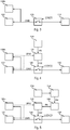
- Figure 7 shows in this respect a possible embodiment of the communication between the configuration module 108 and the configuration data clients 112.
- the processing system 10a comprises a configuration module 108 configured to read the configuration data CD from one or more non-volatile memories 104 and a plurality of configuration data clients 112 configured to receive respective configuration data CD from the configuration module 108 and distribute them among the blocks 110/150/156 requiring configuration data.
- each configuration data client 112 may be associate univocally with a respective block 110/150/156.
- the processing system 10a comprises again three configuration data clients 112a, 112b and 112c.
- the configuration module 108 comprises a data read module 1080 configured to read the configuration data CD from the memory 104 and a dispatch module 1082 configured to transmit the configuration data to the configuration data clients 112.
- any communication may be used for communication between the dispatch module 1082 and the configuration data clients 112.
- the communication between the dispatch module 1082 and the configuration data clients 112 is based on data frames in accordance with a given format, called in the following Device Configuration Format (DCF).
- DCF Device Configuration Format
- each data frame comprises two fields: the payload (i.e., the real data), called DCF Format payload, and possible additional data attributes used to identify the receiver of the data, called DCF Format attributes, wherein the receiver is one of the configuration data clients 112 representing a DCF client.
- the data attributes may consist in 16 or 32 bits, wherein a given number of bits specifies the address of one of the configuration data clients 112, and the payload may consist in 16 or 32 bits.
- the data read module 1080 is configured to read blocks of 64 bits from the memory 104, wherein the first 32 bits contain the data attributes (including the address of a configuration data client) and the second 32 bits contain the configuration data to be transmitted to the address specified in the data attributes.
- each configuration data client/DCF client 112 may be a hardware module, usually comprising a combinational circuit configured to store the received data in an internal register implemented, e.g., with flip-flops/latches, thereby permitting to distribute, via one or more internal signals generated as a function of the data stored in the internal register, the configuration data received to various parts of the associate hardware block(s) 110/150/156.
- each configuration data client 112 may have associated a univocal address (i.e., univocal within each processing system 10a) and analyses the data transmitted by the dispatch module 1082 in order to determine whether the additional data attributes (DCF Format attributes) contain the address associated with the configuration data client 112.
- the module 108 may also comprises a state control module 1084 configured to manage the various configuration phases of the processing system 10a.
- a reset module 116 of the processing system 10a may generate a reset signal RESET, which is used to perform a reset of the various components of the processing system 10a.
- the reset signal RESET may correspond to a reset pulse of a given number of clock cycles, provided to the blocks 110 of the processing system 10a.
- the reset signal RESET may be used by the configuration data clients 112 in order to set the internal register to a given reset value.
- the state control module 1084 may activate the configuration phase. Specifically, during the configuration phase, the data read module 1080 may read the configuration data CD from the memory 104 and the dispatch module 1082 may send the configuration data CD to the various configuration data clients 112, thereby overwriting the reset values.
- the dispatch module 1082 may generate a data signal DATA having a given number of bits (corresponding to the bits of the payload) containing the configuration data to be transmitted to a given configuration data client 112 and further control signals for selecting the target configuration data client 112.
- the dispatch module 1082 generates also an address signal ADR containing the address of the target configuration data client 112 and optionally a chip select signal CS used to signal that the address signal ADR and the data signal DATA are valid.
- the address signal ADR (and the chip select signal CS) may be provided to a decoder 124 configured to activate one of the configuration data clients 112 as a function of the address signal ADD.
- the decoder 124 may set a chip select signal CSa in order to indicate that the configuration data client 112a should read the data signal DATA when the address signal ADR corresponds to an address assigned to the configuration data client 112a (and the chip select signal CS is set).
- the decoder 124 may set a chip select signal CSb in order to indicate that the configuration data client 112b should read the data signal DATA when the address signal ADR corresponds to an address assigned to the configuration data client 112b (and the chip select signal CS is set), etc.
- the configuration data CD may also comprise security configuration data used to configure the protections 150, such as the external access to a debug interface or the (read and/or write) access to given memory locations, and the reference passwords RK to be stored in the temporary password repository 156.
- configuration data CD may comprise two sub-sets of configuration data:
- these groups of configuration data are written to different areas of the memory(ies) 104, thereby permitting that these groups may be configured independently.
- the security configuration data included in the first group of configuration data may also permit to set the access rights to the memory locations, in which the first group of configuration data are stored.
- the first group of configuration data may not be overwritten, and/or the memory interface may inhibit a read access to the first group of configuration data (e.g., by the processing unit 102).
- the security configuration data included in the second group of configuration data may be used to configure the behavior of the blocks 110 from a functional point of view, e.g. in order to enable or disable the debug interface, etc.
- the second group of configuration data may not be overwritten or read.
- the reference password(s) used to unblock the protections may be configured together with the first group and/or secondo group of configuration data.
- the first group may contain a reference password for performing access operations to read and/or write protected memory locations and the second group may contain a reference password for enabling again the debug interface.
- the reset/configuration phase of the processing system 10a is used to store one or more reference passwords RK into a private/local memory (e.g., a RAM) of the temporary password repository 156.
- a private/local memory e.g., a RAM
- the reference passwords RK may be generated during the production phase and programmed into some area of the non-volatile memory 104 (for example some specific memory locations of the program memory 104a).
- the reference password(s) RK are read from the non-volatile memory 104 and distributed to the temporary password repository 156 via dedicated hardware components 108 and 112, e.g. by using the DCF data format.
- the DCF data format permits to transfer different information, programmed inside the non-volatile memory, to various blocks within the processing system 10a using the same data bus. Specifically, each piece of configuration data is inserted in a frame together with the identifier/address of a configuration data client 112.
- the hardware configuration module 108 reads all theses DCF data frames programmed in the non-volatile memory 104 and sends them to the respective configuration data clients 112.
- the reference password(s) RK may be stored in temporary password repository 156.
- the temporary password repository 156 may comprises one or more slots PW0, PW1, ..., each slot being adapted to store a respective reference password RK.
- a single configuration data client 112c is associated with the temporary password repository 156.
- a plurality of DCF frames (each comprising a respective reference password RK) may be sent in sequence to the address of the configured data client 112c and, once a reference password RK is received, the temporary password repository 156 may store the reference password into a respective slot PW0, PW1, ... of the internal memory.
- the DCF frame may also include a field indicating the slot number, where the respective reference password RK should be stored.
- the configuration data clients 112 may also be used directly as memory of the temporary password repository 152.
- these registers may also be used directly as memory of the temporary password repository 152.
- a plurality of configuration data clients 112c may be associated with the temporary password repository 152, wherein each configuration data clients 112c has a respective (univocal) address.
- a plurality of DCF frames (each comprising a respective reference password RK) may be sent in sequence to the addresses of the configured data clients 112c.
- the use of a RAM is advisable when a lot of reference password RK have to be stored into the temporary password repository 156 and/or when the passwords are long.
- the internal register of one or more configuration data clients 112c may be used when only a single reference password RK has to be stored.
- the reference passwords RK are stored in the memory of the temporary password repository 152. Accordingly, there is no need to further access the reference passwords RK stored in the non-volatile memory 104 upon a password challenge request. Accordingly, in the embodiment considered, the communication may not be spied by other blocks of the processing system 10a, because the other blocks are not operative during the configuration phase of the processing system 10a.
- Figure 8 shows an embodiment of the password verification circuit 152.
- the password verification circuit 152 is connected (e.g., directly) to the temporary password repository 156 for receiving a reference password RK to be used for a password verification operation.
- the reference password(s) RK are stored in dedicated areas of the non-volatile memory 104 of the processing system 10a.
- theses reference password(s) RK may be programmed during the production phase.
- the reference password (s) RK may be read (e.g., together with other configuration data CD) by the hardware configuration module 108 of the processing system 10a and distributed to the various configuration data clients 112 within the processing system 10a.
- the distribution of the configuration data CD including the reference password(s) RK may occur during a configuration phase, i.e. when the processing unit 102 and the other blocks (such as communication interfaces 106b) are not yet operative and only the configuration module 108 and the configuration data clients 112 are active.
- the reference password(s) RK are already loaded into the temporary password repository 156, when the processing unit 102 is activated.
- the temporary password repository may contain only a single reference password.
- Figure 9 shows an embodiment, in which the temporary password repository 156 comprises a plurality of slots PW0, PW1, etc. for storing a plurality of reference passwords RK.
- the password verification circuit 152 comprises at least one interface for receiving a password K to be verified.
- the password verification circuit 152 may receive a password verification command VPW including a password K from the processing unit 102 of the processing system 10a.
- the password verification circuit 152 may comprise an interface 1520.
- the processing unit 102 is a microprocessor and the interface 1520 comprises one or more register addressable by the processing unit 102, such as so called special function registers of the processing unit 102.
- the processing unit 102 may provide data to the password verification circuit 152 by writing the content of the registers 1520 via software instructions.
- the password verification circuit 152 may receive data via a communication interface 106b, e.g., from another resource 106 of the processing system 10a or an external processing unit 30.
- a communication interface 106b e.g., from another resource 106 of the processing system 10a or an external processing unit 30.
- the interface 106b may a debug interface, such as a JTAG interface, connected to an external debugger 30.
- the (e.g. debug) interface 106b may indeed be split into a plurality of sub-interfaces connected through a bus 1062, wherein each sub-interface is associated with a respective block of the processing system 10a to be controlled via the ( e . g . debug) interface.
- the interface 1060 which may only manage the debug commands addressed to the password verification circuit 152.
- the interface 1520 or 1060 may thus provide a password verification command VPW including a password K to be verified.
- VPW password verification command
- the interface 1060 may provide a password Ka
- the interface 1520 may provide a password Kb.
- these passwords Ka and Kb are then provided to a multiplexer 1526 configured to select either the password Ka or Kb (based on whether the interface 1060 or 1520 is used).
- the temporary password repository 156 comprises a plurality of slots PW0, PW1,....
- the password verification command VPW may include, and similarly the interfaces 1520 and/or 1060 may provide, additional password configuration data CFG associated with the respective password K to be verified.
- the interface 1060 may provide password configuration information CFGa
- the interface 1520 may provide a password configuration information CFGb.
- the respective password configuration information CFGa and CFGb are then provided to a multiplexer 1528 configured to select either the additional password configuration data CFGa or CFGb (based on whether the interface 1060 or 1520 is used).
- the additional password configuration data CFG may contain a slot number SLOT indicating the slot PW0, PW1, ... of a reference password RK in the temporary password repository 156 to be used for the verification.
- the temporary password repository 156 may provide the respective reference password RK stored in the slot PW0, PW1, ... indicated by the slot number SLOT.
- the password K received via the interface 1060/1520 and the (selected) reference password RK obtained from the temporary password repository 156 are provided to a comparison circuit 1522 configured to determine whether the password K corresponds to the (selected) reference password RK. In case the password K corresponds to the (selected) reference password RK, the comparison circuit 1522 generates an overwrite signal OW indicating that the password K is correct, i.e. the password K corresponds to the (selected) reference password RK.
- the password verification circuit 152 supports only a single reference password RK (i.e., the temporary password repository comprises only a single slot).
- the signal OW may be sent directly to one or more of the protections circuits 150, which thus may deactivate the respective protection.
- each protection circuit 150 may not only take into account the signal OW, but also further configuration information, such as the previously mentioned life cycle data LCD and/or configuration data CD, which may indicate whether the protection may indeed be deactivated or not by means of the signal OW.
- the password verification circuit 152 supports a plurality of reference passwords RK (i.e., the temporary password repository 156 comprises a plurality of slots).
- the signal OW may be sent to a circuit 1524.
- the circuit 1524 is configured to generate a plurality of overwrite signals OW0, OW1, ... as a function of the signal OW and the slot number SLOT.
- the block 1524 may be implemented with a combinational circuit or a look-up table.
- a respective overwrite signal OW0, OW1, ... is associated with each slot, and only the overwrite signal OW0, OW1, ... associated with the currently used slot SLOT is set (e.g., to the logic level high) when the password K and RK match.
- the circuit 1524 may also comprises registers, e.g. flip-flops or latches, for storing the values of the overwrite signal OW0, OW1, ..., thereby maintain the value of the overwrite signals OW0, OW1, ... when a new password verification is requested.
- the overwrite signals OW0, OW1, ... may then be provided to the various protection circuits 150, which thus may deactivate the respective protection.
- a respective overwrite signal OW0, OW1, ... may be associated with each protection circuit 150, or each overwrite signal OW0, OW1, ... may be associated also with a plurality of protection circuits 150.
- the circuit 1524 is configured to associate with each slot number a respective subset of protection circuits 150. Moreover, when the password received K corresponds to the reference password RK for a given slot SLOT, the circuit 1524 generates one or more signals OW0, OW1, ... in order to inform the subset of protection circuits 150 associated with the given slot SLOT that the passwords match.
- each protection circuit 150 may deactivate the respective protection not only as a function of the respective signal OW, but also as a function of further configuration information, such as the previously mentioned life cycle data LCD or configuration data CD, which may indicate whether the protection may be deactivated or not by means of the password verification.
- each slot PW0, PW1, ... contains a given reference password RK and the slot index SLOT determines (via the circuit 1524), which protection circuit 150 is regulated by the password.
- a given slot number e.g ., slot 3
- the protection circuit 150 controlling access to the debug interface, e.g ., the access of the external debugger 30 to the debug bus 1062.
- a given slot number e.g ., slot 2
- the protection circuit 150 regulating read and/or write access to the non-volatile memory 104.
- a given slot number (e.g ., slot 1) may represent also a master password (e.g ., written by the producer of the processing system 10a), which is associated with all protection circuits 150. Accordingly, neglecting that also further life cycle data LCD and/or configuration data CD may be taken into account, a protection may be removed by providing the correct password stored in a slot associated with the respective protection 150.
- the password management is split into three functional blocks:
- the temporary password repository 156 is used as a secure repository for the reference passwords RK, while the password verification circuit 152 processes password challenge requests received via the interfaces 1060 and/or 1520 and provides the result to the connected protection circuits 150.
- the password challenge requests i.e. the password verification commands VPW
- the password verification commands VPW may be received:
- the interfaces 1520 and 1060 have the same basic functionality, i.e ., provide a password K and possible additional configuration information CFG to the password verification circuit 152.
- a single interface could be used, e.g., in case the processing unit 102 is also connected to the bus 1062.
- the interface 1520 may be a register interface specifically adapted to interface the processing unit 102.
- the interface 1520 may be a special function register of a microprocessor and programmed directly via software instructions executed by the processing unit 102.
- the interface 1060 may be part of debug interface 106b, such as a JTAG interface.
- various blocks of the processing system may have associated debug interfaces, which may also be connected through a debug bus 1062. Accordingly, a certain protection mechanism could be removed by providing a proper password through this debug interface (in case at least the portion 1060 of the debug interface associated with the password verification circuit 152 is not deactivated).
- a protection circuit 150 could be configured to deactivate the debug interface of the processing unit 102, e.g., based on the life cycle data LCD and/or the configuration data CD.
- the debug interface of the processing unit 102 may be connected to the bus 1062.
- an external debugger 30 could be used to provide a password K to the debug interface 1060 of the password verification circuit 152 and the password verification circuit 152 may generate the signal OW (or similarly one or more signals OW0, OW1, etc.), which is sent to the protection circuit 150 associated with the debug interface of the processing unit 102.
- the protection circuit 150 may then reactivate the debug interface of the processing unit 102, and a developer may use the external debugger 30 to analyze the processing unit 102.
- the interface 1060 may be part of the (e.g., debug) interface 106b.
- the specific protocol used to write data to the interface 1060 depends on the specific implementation of the interface 106b.
- the most common protocols are based on request and busy signals.
- the busy signal may be set by the password verification circuit 152 to communicate that the password verification circuit is performing already an operation, i.e. no password challenge requests are accepted.
- the request signal may be set by the hardware client requesting a password challenge (only after the busy signal has been de-asserted).
- the hardware client requesting a password challenge provides the password verification command VPW including the password to be verified K and if supported the additional password configuration information CFG, such as the password slot number SLOT.
- the register interface 1520 may comprise a busy flag, to advice the processing unit 102 when the password verification circuit 152 is busy, and means for starting a challenge operation (such as a request flag), a register for storing the password to be verified K and optionally the further configuration data, in particular the slot index SLOT.
- Figure 10 shows an embodiment of the register interface 1520.
- the interface 1520 comprises:
- the processing unit 102 may execute the following steps:
- the password verification circuit 152 may set the busy flag in order to indicate that the password verification circuit 152 does not accepts any other password challenge request.
- the comparison circuit 1522 If the password K provided by the client matches the reference password RK stored in the given slot SLOT, then the comparison circuit 1522 generates the overwrite signal OW indicating that the access may be granted.
- the block 1524 may also provide respective overwrite signals OW0, OW1, ... only for a subset of the protection circuits 150.
- the protection circuit 150 may decide whether the protection should indeed be disabled.
- each protection circuit 150 may take into account for this purpose the life cycle data LCD and/or the configuration data CD.
- each protection circuit 150 may take into account also the identity of the circuit having requested the password verification.
- the interface 1520 accepts only requests from the processing unit 102. Accordingly, the identity of the requesting circuit may be determined implicitly.
- the interface 1060 may be connected to a bus 1062. Accordingly, in this case, each device connected to the bus 1062 may be identified with a given address (being univocal within the processing system 10a).
- the interface 1520 may be connected to a bus, e.g. in case the processing system 10a comprises a plurality of processing units, such as a plurality of microprocessors.
- the identity of the circuit requesting the verification of a password may correspond to the univocal address of the block within the processing system 10a and will be called in the following master identification MID.
- Figure 11 shows an embodiment, wherein this identification MID is provided by the interfaces 1060 and 1520 together with the additional configuration information CFG.
- the number of the overwrite signal OW0, OW1, ... corresponds to the number N of slots in the temporary password repository 156, i.e ., a respective signal OW0, OW1, ... is univocally associated with a respective slot. Accordingly, by providing the correct password K for a given slot SLOT, only the respective overwrite signal OW0, OW1, ... will be set, e.g ., the signal OW0 will be set for the password PW0, the signal OW1 will be set for the password PW1, etc. As mentioned before, the overwrite signals OW0, OW1, ... may also be stored in registers, thereby permitting that plural overwrite signal OW0, OW1, ... may be set by providing sequentially the passwords for the various slots.
- the block 1524 when setting an overwrite signal OW0, OW1, ..., stores for the specific overwrite signal OW0, OW1, ... also the identification MID of the circuit having requested the password verification, i.e . the circuit 1524 provides indeed N identification MID0, MID1, .... Accordingly, in the embodiment considered, once having verified that the password K corresponds to the reference password RK for the selected SLOT, not only the respective overwrite signal is set, but also the current identification MID is stored as the identification MID0, MID1, ... associated with the respective SLOT.
- the protection circuits 150 do not receive only the overwrite signal OW0, OW1, ..., but also the respective identification MID0, MID1, ....
- each password slot PW0, PW1, ... may be associated univocally with a single protection circuit 150, i.e. each password may only unblock the respective protection circuit 150. Accordingly, also the overwrite signal and the respective IDs MID associated with a given slot have to be provided only to the respective protection circuit 150.
- the number of slots N may be defined at design time, depending on how many protection circuits 150 with an associated password-dependent protection mechanism exist. Moreover, it is also simple to add a new additional protection circuit 150, by just adding a new reference password slot, and a new overwrite signal OV and identification MID output.
- the protection circuits 150 may use the identification MID for different purposes.
- a protection circuit 150 may disable the protection only when the request comes from a circuit having a given identification MID. For example, in case of a multiprocessor system, when the request comes from a given microprocessor 102.
- the protection circuit 150 may verify whether a given access request to the block 110 associated with the protection circuit (see also Figure 5 ) has the same identification MID as the circuit having requested the password verification. Accordingly, the identification MID can be used by the protection circuits 150 to limit the access to the protected resource 110 only to the circuit identified by the same identification MID, thereby ensuring that only the circuit having provided the correct password may also access the respective protected resource 110.
- a first circuit may deactivate a first protection 150 by providing the first reference password PW0, and a second circuit may deactivate a second protection by providing the second reference password PW1, wherein the second circuit does not have access to the first protection.
- the password verification circuit 152 may verify whether the password K provided by the requester client has a special value (e.g., all-1, all-0, etc.) which will result always in a comparison failure.
- a special value e.g., all-1, all-0, etc.
Landscapes
- Engineering & Computer Science (AREA)
- Theoretical Computer Science (AREA)
- Computer Hardware Design (AREA)
- Computer Security & Cryptography (AREA)
- Physics & Mathematics (AREA)
- General Physics & Mathematics (AREA)
- General Engineering & Computer Science (AREA)
- Software Systems (AREA)
- Mathematical Physics (AREA)
- Health & Medical Sciences (AREA)
- Bioethics (AREA)
- General Health & Medical Sciences (AREA)
- Storage Device Security (AREA)
Claims (10)
- Verarbeitungssystem (10a), Folgendes umfassend:- einen nicht-flüchtigen Speicher, (104) angepasst, um wenigstens ein Referenz-Passwort (RK) zu speichern;- eine Passwort-Verifizierungs-Schaltung (152), konfiguriert, um:a) einen Passwort-Verifizierungs-Befehl (VPW) zu empfangen, ein Passwort (K) enthaltend;b) eines von dem wenigstens einen in dem nicht-flüchtigen Speicher (104) gespeicherten Referenzpasswort (RK) zu erhalten;c) zu testen, ob das empfangene Passwort (K) und das eine Referenzpasswort (RK) einander entsprechen; undd) wenn der Test indiziert, dass das Passwort (K) und das eine Referenzpasswort (RK) einander entsprechen, ein Überschreibungssignal (OW; OW0, OW1) zu erzeugen;- einen Hardware-Block (110) und eine mit dem Hardware-Block (110) assoziierte Schutzschaltung (150), wobei die Schutzschaltung (150) konfiguriert ist, um einen Steuerungsbefehl (CMD) zu empfangen und den Steuerungsbefehl (CMD) als Funktion des Überschreibungssignals (OW; OW0, OW1) selektiv an den Hardwareblock (110) weiterzuleiten; und- eine Verarbeitungseinheit (102) und/oder eine Kommunikationsschnittstelle (106b), konfiguriert, um den Steuerungsbefehl (CMD) bereitzustellen, um den Betrieb des Hardwareblocks (110) zu steuern und den Passwort-Verifizierungs-Befehl (VPW), das Passworts (K) enthaltend, zu verifizieren;- ein temporäres Passwort-Repositorium (156), einen Speicher enthaltend, angepasst, um das wenigstens eine Referenzpasswort (RK) zu speichern, wobei die Passwort-Verifizierungs-Schaltung (152) konfiguriert ist, um das eine Referenzpasswort (RK) von dem temporären Passwort-Repositorium (156) zu erhalten; und- eine Passwort-Hochlade-Schaltung (154; 108, 112), konfiguriert, um das wenigstens eine Referenzpasswort (RK) aus dem nicht-flüchtigen Speicher (104) auszulesen und das wenigstens eine aus dem nicht-flüchtigen Speicher (104) ausgelesene Referenzpasswort (RK) in dem temporären Passwort-Repositorium (156) zu speichern;dadurch gekennzeichnet, dass das Verarbeitungssystem (10a) Folgendes umfasst:- den wenigstens einen Hardwareblock (110) und/oder Schutzschaltung (150), konfiguriert, um den Betrieb als Funktion der Konfigurationsdaten (CD) zu ändern, wobei der nicht-flüchtige Speicher (104) angepasst ist, um die Konfigurationsdaten (CD) zu speichern, wobei das wenigstens eine Referenzpasswort (RK) zusammen mit den Konfigurationsdaten (CD) in dem nicht-flüchtigen Speicher (104) gespeichert ist;- wenigstens einen ersten Konfigurationsdaten-Client (112a, 112b), assoziiert mit dem wenigstens einen Hardwareblock (110) und/oder der Schutzschaltung (150), konfiguriert, um den Betrieb als Funktion der Konfigurationsdaten (CD) zu ändern, wobei der wenigstens eine erste Konfigurationsdaten-Client (112a, 112b), konfiguriert ist, um Konfigurationsdaten (CD) zu empfangen und die empfangenen Konfigurationsdaten (CD) dem assoziierten wenigstens einen Hardwareblock (110) und/oder der Schutzschaltung (150) bereitzustellen,- ein Hardware-Konfigurationsmodul (108), konfiguriert, um die Konfigurationsdaten (CD) aus dem nicht-flüchtigen Speicher (104) auszulesen und um die aus dem nicht-flüchtigen Speicher (104) ausgelesenen Konfigurationsdaten an den ersten Konfigurationsdaten-Client (112a, 112b) zu übertragen;- wenigstens einen zweiten Konfigurationsdaten-Client (112c), wobei der wenigstens eine zweite Konfigurationsdaten-Client (112c) konfiguriert ist, um Konfigurationsdaten (CD) von dem Hardware-Konfigurationsmodul (108) zu empfangen und die empfangenen Konfigurationsdaten (CD) dem temporären Passwort-Repositorium (156) bereitzustellen, wobei wenn das Hardware-Konfigurationsmodul (108) die Konfigurationsdaten (CD) aus dem nicht-flüchtigen Speicher (104) ausliest, das Hardware-Konfigurations-Modul (108) das wenigstens eine Referenzpasswort (RK) an den wenigstens einen zweiten Konfigurationsdaten-Client (112c) überträgt; und- eine Zurücksetzungsschaltung (116), konfiguriert, um ein Zurücksetzungssignal (RESET) zu erzeugen, wenn das Verarbeitungssystem (10a) eingeschaltet wird, und wobei das Hardware-Konfigurationsmodul (108) konfiguriert ist, um die Konfigurationsdaten (CD) aus dem nicht-flüchtigen Speicher (104) auszulesen und als Reaktion auf das Zurücksetzungssignal (RESET) die aus dem nicht-flüchtigen Speicher (104) ausgelesenen Konfigurationsdaten (CD) an den wenigstens einen ersten Konfigurationsdaten-Client (112a, 112b) und den wenigstens einen zweiten Konfigurationsdaten-Client (112a, 112b) zu übertragen.
- Verarbeitungssystem (10a) nach Anspruch 1, wobei jeder von dem wenigstens einen ersten Konfigurationsdaten-Client (112a, 112b) und dem wenigstens einen zweiten Konfigurationsdaten-Client (112c) ein Register umfasst und eine entsprechende assoziierte Adresse aufweist, wobei das Hardware-Konfigurationsmodul (108) Folgendes umfasst:- ein Dispositionsmodul (1082), konfiguriert, um ein Adresssignal (ADR) zu erzeugen, die Adresse eines Ziel-Konfigurationsdaten-Clients (112) umfassend, ausgewählt aus dem wenigstens einen ersten Konfigurationsdaten-Client (112a, 112b) und dem wenigstens einen zweiten Konfigurationsdaten-Client (112c), und ein Datensignal (DATA), die in dem Register des Ziel-Konfigurationsdaten-Clients (112) zu speichernden Konfigurationsdaten umfassend;- ein Daten-Auslesemodul (1080), konfiguriert, um die Konfigurationsdaten (CD) aus dem nicht-flüchtigen Speicher (104) auszulesen und um dem Hardware-Dispositions-Modul (1082) die aus dem nicht-flüchtigen Speicher (104) ausgelesenen Konfigurationsdaten (CD) bereitzustellen.
- Verarbeitungssystem (10a) nach Anspruch 2, wobei die Konfigurationsdaten (CD) in dem nicht-flüchtigen Speicher (104) in der Form von Datenrahmen gespeichert sind, umfassend ein Attributfeld umfassend die Adresse eines Ziel-Konfigurationsdaten-Clients (112) und als Nutzlast die entsprechenden Konfigurationsdaten.
- Verarbeitungssystem (10a) nach Anspruch 1, wobei die Passwort-Hochlade-Schaltung (154; 108, 112) konfiguriert ist, um das wenigstens eine Referenzpasswort (RK) aus dem nicht-flüchtigen Speicher (104) auszulesen und um das wenigstens eine aus dem nicht-flüchtigen Speicher (104) ausgelesene Referenzpasswort (RK) in dem temporären Passwort-Repositorium (156) zu speichern, wenn das Verarbeitungssystem (10a) eingeschaltet wird und die Verarbeitungseinheit (102) und/oder eine Kommunikationsschnittstelle (106b) noch nicht funktionstüchtig ist.
- Verarbeitungssystem (10a) nach einem der vorhergehenden Ansprüche, umfassend einen Kommunikationsbus (1062), beispielsweise einen JTAG-Bus, wobei der Hardwareblock (110) zum Empfangen des Steuerungsbefehls (CMD) mit dem Kommunikationsbus (1062) verbunden ist, und wobei die Passwort-Verifizierungsschaltung (152) eine erste, zum Empfangen des Passwort-Verifizierungs-Befehls (VPW) mit dem Kommunikationsbus (1062) verbundene Schnittstelle (1060) umfasst.
- Verarbeitungssystem (10a) nach einem der vorhergehenden Ansprüche, wobei die Passwort-Verifizierungsschaltung (152) eine zweite Schnittstelle (1520) zum Empfangen des Passwort-Verifizierungs-Befehls (VPW) von der Verarbeitungseinheit (102) umfasst, wobei es sich bei der Verarbeitungseinheit (102) um einen Mikroprozessor handelt und die zweite Schnittstelle (1520) wenigstens ein von den Mikroprozessor-Anweisungen adressierbares Register umfasst.
- Verarbeitungssystem (10a) nach einem der vorhergehenden Ansprüche, wobei das temporäre Passwort-Repositorium (156) eine Vielzahl von Slots (PWO, PW1) zum Speichern einer Vielzahl von Referenzpasswörtern (RK) umfasst, wobei der Passwort-Verifizierungs-Befehl (VPW) ein Feld zum Spezifizieren einer Slot-Nummer (SLOT) enthält, und wobei das temporäre Passwort-Repositorium (156) konfiguriert ist, um das in dem von der Slotnummer (SLOT) indizierten Slot gespeicherte Referenzpasswort (RK) bereitzustellen.
- Verarbeitungssystem (10a) nach Anspruch 7, wobei die Passwort-Verifizierungsschaltung (152) konfiguriert ist, um für jeden Slot (PWO, PW1) ein entsprechendes Überschreibungssignal (OW0, OW1) zu generieren, indizierend, dass das empfangene Passwort (K) und das in dem von der Slotnummer (SLOT) indizierten Slot gespeicherte Referenzpasswort (RK) einander entsprechen.
- Verarbeitungssystem (10a) nach einem der vorhergehenden Ansprüche, wobei die Passwort-Verifizierungsschaltung (152) konfiguriert ist, um, wenn der Test indiziert, dass das Passwort (K) und das eine Referenzpasswort (RK) einander entsprechen, ein Signal (MID) zu übertragen, eine Identifizierung der Verarbeitungseinheit (102) umfassend, und/oder wobei die Kommunikationsschnittstelle (106b) der Schutzschaltung (150) einen Passwort-Verifizierungs-Befehl (VPW) bereitstellt.
- Integrierte Schaltung, beispielsweise ein Mikro-Controller, umfassend ein Verarbeitungssystem (10a) nach einem der Ansprüche 1 bis 9.
Applications Claiming Priority (1)
| Application Number | Priority Date | Filing Date | Title |
|---|---|---|---|
| IT102017000082176A IT201700082176A1 (it) | 2017-07-19 | 2017-07-19 | Sistema di elaborazione, relativo circuito integrato e procedimento |
Publications (2)
| Publication Number | Publication Date |
|---|---|
| EP3432190A1 EP3432190A1 (de) | 2019-01-23 |
| EP3432190B1 true EP3432190B1 (de) | 2020-09-23 |
Family
ID=60294332
Family Applications (1)
| Application Number | Title | Priority Date | Filing Date |
|---|---|---|---|
| EP18182223.0A Active EP3432190B1 (de) | 2017-07-19 | 2018-07-06 | Verarbeitungssystem und integrierter schaltungschip für passwortverwaltung |
Country Status (3)
| Country | Link |
|---|---|
| US (1) | US10949570B2 (de) |
| EP (1) | EP3432190B1 (de) |
| IT (1) | IT201700082176A1 (de) |
Families Citing this family (3)
| Publication number | Priority date | Publication date | Assignee | Title |
|---|---|---|---|---|
| WO2020208639A2 (en) * | 2019-04-11 | 2020-10-15 | Saferide Technologies Ltd | A system and method for detection of anomalous controller area network (can) messages |
| IT202100007475A1 (it) | 2021-03-26 | 2022-09-26 | Stmicroelectronics Application Gmbh | Sistema di elaborazione, relativo circuito integrato, dispositivo e procedimento |
| IT202100030332A1 (it) | 2021-11-30 | 2023-05-30 | Stmicroelectronics Application Gmbh | Sistema di elaborazione, relativo circuito integrato, dispositivo e procedimento |
Family Cites Families (13)
| Publication number | Priority date | Publication date | Assignee | Title |
|---|---|---|---|---|
| FR2675602B1 (fr) * | 1991-04-16 | 1995-04-14 | Hewlett Packard Co | Procede et dispositif de protection d'un systeme informatique. |
| JP3424547B2 (ja) * | 1998-02-26 | 2003-07-07 | 株式会社日立製作所 | 液体クロマトグラフ |
| US6145085A (en) * | 1998-04-30 | 2000-11-07 | Compaq Computer Corporation | Method and apparatus for providing remote access to security features on a computer network |
| US6510522B1 (en) * | 1998-11-20 | 2003-01-21 | Compaq Information Technologies Group, L.P. | Apparatus and method for providing access security to a device coupled upon a two-wire bidirectional bus |
| US20030233534A1 (en) * | 2002-06-12 | 2003-12-18 | Adrian Bernhard | Enhanced computer start-up methods |
| US7904839B2 (en) * | 2007-12-12 | 2011-03-08 | International Business Machines Corporation | System and method for controlling access to addressable integrated circuits |
| US9612977B2 (en) * | 2011-07-15 | 2017-04-04 | Standard Microsystems Corporation | Method and system for controlling access to embedded nonvolatile memories |
| US9343177B2 (en) * | 2013-02-01 | 2016-05-17 | Apple Inc. | Accessing control registers over a data bus |
| US20150331043A1 (en) * | 2014-05-15 | 2015-11-19 | Manoj R. Sastry | System-on-chip secure debug |
| US9792435B2 (en) * | 2014-12-30 | 2017-10-17 | Battelle Memorial Institute | Anomaly detection for vehicular networks for intrusion and malfunction detection |
| US9792229B2 (en) * | 2015-03-27 | 2017-10-17 | Intel Corporation | Protecting a memory |
| IT201700062788A1 (it) | 2017-06-08 | 2018-12-08 | Stmicroelectronics Application Gmbh | Sistema di elaborazione, relativo circuito integrato, dispositivo e procedimento |
| IT201700062830A1 (it) | 2017-06-08 | 2018-12-08 | Stmicroelectronics Application Gmbh | Sistema di elaborazione, relativo circuito integrato, dispositivo e procedimento |
-
2017
- 2017-07-19 IT IT102017000082176A patent/IT201700082176A1/it unknown
-
2018
- 2018-07-06 EP EP18182223.0A patent/EP3432190B1/de active Active
- 2018-07-18 US US16/039,103 patent/US10949570B2/en active Active
Non-Patent Citations (1)
| Title |
|---|
| None * |
Also Published As
| Publication number | Publication date |
|---|---|
| US20190026498A1 (en) | 2019-01-24 |
| EP3432190A1 (de) | 2019-01-23 |
| US10949570B2 (en) | 2021-03-16 |
| IT201700082176A1 (it) | 2019-01-19 |
Similar Documents
| Publication | Publication Date | Title |
|---|---|---|
| US11281807B2 (en) | Processing system, related integrated circuit and method | |
| US11474752B2 (en) | Processing system including one-time programmable memory with original life cycle data, related integrated circuit, device and method | |
| CN100371906C (zh) | 用于确定访问许可的方法和设备 | |
| US11068255B2 (en) | Processing system, related integrated circuit, device and method | |
| US10922015B2 (en) | Processing system, related integrated circuit, device and method | |
| US10855529B2 (en) | Processing system, related integrated circuit, device and method | |
| US10845999B2 (en) | Processing system, related integrated circuit, device and method | |
| US11210161B2 (en) | Processing system, related integrated circuit, device and method | |
| US20140025871A1 (en) | Processor system and control method thereof | |
| EP3432190B1 (de) | Verarbeitungssystem und integrierter schaltungschip für passwortverwaltung | |
| CN115129511B (zh) | 处理系统、相关集成电路、设备和方法 | |
| EP4187415B1 (de) | Verarbeitungssystem, zugehörige vorrichtung und verfahren zum schützen von verriegelungen oder flip-flops eines registers | |
| US20260128898A1 (en) | Processing system, related integrated circuit, device and method | |
| EP4296850B1 (de) | Verarbeitungssystem, zugehörige integrierte schaltung, vorrichtung und verfahren | |
| CN121996584A (zh) | 处理系统、相关集成电路、设备及方法 | |
| CN120724424A (zh) | 信息保护方法、系统、控制器、处理器、设备、介质 |
Legal Events
| Date | Code | Title | Description |
|---|---|---|---|
| PUAI | Public reference made under article 153(3) epc to a published international application that has entered the european phase |
Free format text: ORIGINAL CODE: 0009012 |
|
| STAA | Information on the status of an ep patent application or granted ep patent |
Free format text: STATUS: THE APPLICATION HAS BEEN PUBLISHED |
|
| AK | Designated contracting states |
Kind code of ref document: A1 Designated state(s): AL AT BE BG CH CY CZ DE DK EE ES FI FR GB GR HR HU IE IS IT LI LT LU LV MC MK MT NL NO PL PT RO RS SE SI SK SM TR |
|
| AX | Request for extension of the european patent |
Extension state: BA ME |
|
| STAA | Information on the status of an ep patent application or granted ep patent |
Free format text: STATUS: REQUEST FOR EXAMINATION WAS MADE |
|
| 17P | Request for examination filed |
Effective date: 20190702 |
|
| RBV | Designated contracting states (corrected) |
Designated state(s): AL AT BE BG CH CY CZ DE DK EE ES FI FR GB GR HR HU IE IS IT LI LT LU LV MC MK MT NL NO PL PT RO RS SE SI SK SM TR |
|
| GRAP | Despatch of communication of intention to grant a patent |
Free format text: ORIGINAL CODE: EPIDOSNIGR1 |
|
| STAA | Information on the status of an ep patent application or granted ep patent |
Free format text: STATUS: GRANT OF PATENT IS INTENDED |
|
| INTG | Intention to grant announced |
Effective date: 20200428 |
|
| GRAS | Grant fee paid |
Free format text: ORIGINAL CODE: EPIDOSNIGR3 |
|
| GRAA | (expected) grant |
Free format text: ORIGINAL CODE: 0009210 |
|
| STAA | Information on the status of an ep patent application or granted ep patent |
Free format text: STATUS: THE PATENT HAS BEEN GRANTED |
|
| AK | Designated contracting states |
Kind code of ref document: B1 Designated state(s): AL AT BE BG CH CY CZ DE DK EE ES FI FR GB GR HR HU IE IS IT LI LT LU LV MC MK MT NL NO PL PT RO RS SE SI SK SM TR |
|
| REG | Reference to a national code |
Ref country code: GB Ref legal event code: FG4D |
|
| REG | Reference to a national code |
Ref country code: CH Ref legal event code: EP |
|
| REG | Reference to a national code |
Ref country code: IE Ref legal event code: FG4D |
|
| REG | Reference to a national code |
Ref country code: DE Ref legal event code: R096 Ref document number: 602018008026 Country of ref document: DE Ref country code: AT Ref legal event code: REF Ref document number: 1317125 Country of ref document: AT Kind code of ref document: T Effective date: 20201015 |
|
| PG25 | Lapsed in a contracting state [announced via postgrant information from national office to epo] |
Ref country code: GR Free format text: LAPSE BECAUSE OF FAILURE TO SUBMIT A TRANSLATION OF THE DESCRIPTION OR TO PAY THE FEE WITHIN THE PRESCRIBED TIME-LIMIT Effective date: 20201224 Ref country code: NO Free format text: LAPSE BECAUSE OF FAILURE TO SUBMIT A TRANSLATION OF THE DESCRIPTION OR TO PAY THE FEE WITHIN THE PRESCRIBED TIME-LIMIT Effective date: 20201223 Ref country code: HR Free format text: LAPSE BECAUSE OF FAILURE TO SUBMIT A TRANSLATION OF THE DESCRIPTION OR TO PAY THE FEE WITHIN THE PRESCRIBED TIME-LIMIT Effective date: 20200923 Ref country code: BG Free format text: LAPSE BECAUSE OF FAILURE TO SUBMIT A TRANSLATION OF THE DESCRIPTION OR TO PAY THE FEE WITHIN THE PRESCRIBED TIME-LIMIT Effective date: 20201223 Ref country code: SE Free format text: LAPSE BECAUSE OF FAILURE TO SUBMIT A TRANSLATION OF THE DESCRIPTION OR TO PAY THE FEE WITHIN THE PRESCRIBED TIME-LIMIT Effective date: 20200923 Ref country code: FI Free format text: LAPSE BECAUSE OF FAILURE TO SUBMIT A TRANSLATION OF THE DESCRIPTION OR TO PAY THE FEE WITHIN THE PRESCRIBED TIME-LIMIT Effective date: 20200923 |
|
| REG | Reference to a national code |
Ref country code: AT Ref legal event code: MK05 Ref document number: 1317125 Country of ref document: AT Kind code of ref document: T Effective date: 20200923 |
|
| PG25 | Lapsed in a contracting state [announced via postgrant information from national office to epo] |
Ref country code: LV Free format text: LAPSE BECAUSE OF FAILURE TO SUBMIT A TRANSLATION OF THE DESCRIPTION OR TO PAY THE FEE WITHIN THE PRESCRIBED TIME-LIMIT Effective date: 20200923 Ref country code: RS Free format text: LAPSE BECAUSE OF FAILURE TO SUBMIT A TRANSLATION OF THE DESCRIPTION OR TO PAY THE FEE WITHIN THE PRESCRIBED TIME-LIMIT Effective date: 20200923 |
|
| REG | Reference to a national code |
Ref country code: NL Ref legal event code: MP Effective date: 20200923 |
|
| REG | Reference to a national code |
Ref country code: LT Ref legal event code: MG4D |
|
| PG25 | Lapsed in a contracting state [announced via postgrant information from national office to epo] |
Ref country code: LT Free format text: LAPSE BECAUSE OF FAILURE TO SUBMIT A TRANSLATION OF THE DESCRIPTION OR TO PAY THE FEE WITHIN THE PRESCRIBED TIME-LIMIT Effective date: 20200923 Ref country code: SM Free format text: LAPSE BECAUSE OF FAILURE TO SUBMIT A TRANSLATION OF THE DESCRIPTION OR TO PAY THE FEE WITHIN THE PRESCRIBED TIME-LIMIT Effective date: 20200923 Ref country code: CZ Free format text: LAPSE BECAUSE OF FAILURE TO SUBMIT A TRANSLATION OF THE DESCRIPTION OR TO PAY THE FEE WITHIN THE PRESCRIBED TIME-LIMIT Effective date: 20200923 Ref country code: PT Free format text: LAPSE BECAUSE OF FAILURE TO SUBMIT A TRANSLATION OF THE DESCRIPTION OR TO PAY THE FEE WITHIN THE PRESCRIBED TIME-LIMIT Effective date: 20210125 Ref country code: RO Free format text: LAPSE BECAUSE OF FAILURE TO SUBMIT A TRANSLATION OF THE DESCRIPTION OR TO PAY THE FEE WITHIN THE PRESCRIBED TIME-LIMIT Effective date: 20200923 Ref country code: EE Free format text: LAPSE BECAUSE OF FAILURE TO SUBMIT A TRANSLATION OF THE DESCRIPTION OR TO PAY THE FEE WITHIN THE PRESCRIBED TIME-LIMIT Effective date: 20200923 |
|
| PG25 | Lapsed in a contracting state [announced via postgrant information from national office to epo] |
Ref country code: PL Free format text: LAPSE BECAUSE OF FAILURE TO SUBMIT A TRANSLATION OF THE DESCRIPTION OR TO PAY THE FEE WITHIN THE PRESCRIBED TIME-LIMIT Effective date: 20200923 Ref country code: IS Free format text: LAPSE BECAUSE OF FAILURE TO SUBMIT A TRANSLATION OF THE DESCRIPTION OR TO PAY THE FEE WITHIN THE PRESCRIBED TIME-LIMIT Effective date: 20210123 Ref country code: ES Free format text: LAPSE BECAUSE OF FAILURE TO SUBMIT A TRANSLATION OF THE DESCRIPTION OR TO PAY THE FEE WITHIN THE PRESCRIBED TIME-LIMIT Effective date: 20200923 Ref country code: AT Free format text: LAPSE BECAUSE OF FAILURE TO SUBMIT A TRANSLATION OF THE DESCRIPTION OR TO PAY THE FEE WITHIN THE PRESCRIBED TIME-LIMIT Effective date: 20200923 Ref country code: AL Free format text: LAPSE BECAUSE OF FAILURE TO SUBMIT A TRANSLATION OF THE DESCRIPTION OR TO PAY THE FEE WITHIN THE PRESCRIBED TIME-LIMIT Effective date: 20200923 |
|
| REG | Reference to a national code |
Ref country code: DE Ref legal event code: R097 Ref document number: 602018008026 Country of ref document: DE |
|
| PG25 | Lapsed in a contracting state [announced via postgrant information from national office to epo] |
Ref country code: SK Free format text: LAPSE BECAUSE OF FAILURE TO SUBMIT A TRANSLATION OF THE DESCRIPTION OR TO PAY THE FEE WITHIN THE PRESCRIBED TIME-LIMIT Effective date: 20200923 |
|
| PLBE | No opposition filed within time limit |
Free format text: ORIGINAL CODE: 0009261 |
|
| STAA | Information on the status of an ep patent application or granted ep patent |
Free format text: STATUS: NO OPPOSITION FILED WITHIN TIME LIMIT |
|
| PG25 | Lapsed in a contracting state [announced via postgrant information from national office to epo] |
Ref country code: SI Free format text: LAPSE BECAUSE OF FAILURE TO SUBMIT A TRANSLATION OF THE DESCRIPTION OR TO PAY THE FEE WITHIN THE PRESCRIBED TIME-LIMIT Effective date: 20200923 Ref country code: DK Free format text: LAPSE BECAUSE OF FAILURE TO SUBMIT A TRANSLATION OF THE DESCRIPTION OR TO PAY THE FEE WITHIN THE PRESCRIBED TIME-LIMIT Effective date: 20200923 |
|
| 26N | No opposition filed |
Effective date: 20210624 |
|
| PG25 | Lapsed in a contracting state [announced via postgrant information from national office to epo] |
Ref country code: IT Free format text: LAPSE BECAUSE OF FAILURE TO SUBMIT A TRANSLATION OF THE DESCRIPTION OR TO PAY THE FEE WITHIN THE PRESCRIBED TIME-LIMIT Effective date: 20200923 |
|
| REG | Reference to a national code |
Ref country code: CH Ref legal event code: PL |
|
| PG25 | Lapsed in a contracting state [announced via postgrant information from national office to epo] |
Ref country code: MC Free format text: LAPSE BECAUSE OF FAILURE TO SUBMIT A TRANSLATION OF THE DESCRIPTION OR TO PAY THE FEE WITHIN THE PRESCRIBED TIME-LIMIT Effective date: 20200923 |
|
| REG | Reference to a national code |
Ref country code: BE Ref legal event code: MM Effective date: 20210731 |
|
| PG25 | Lapsed in a contracting state [announced via postgrant information from national office to epo] |
Ref country code: LI Free format text: LAPSE BECAUSE OF NON-PAYMENT OF DUE FEES Effective date: 20210731 Ref country code: CH Free format text: LAPSE BECAUSE OF NON-PAYMENT OF DUE FEES Effective date: 20210731 |
|
| PG25 | Lapsed in a contracting state [announced via postgrant information from national office to epo] |
Ref country code: LU Free format text: LAPSE BECAUSE OF NON-PAYMENT OF DUE FEES Effective date: 20210706 Ref country code: FR Free format text: LAPSE BECAUSE OF NON-PAYMENT OF DUE FEES Effective date: 20210731 |
|
| PG25 | Lapsed in a contracting state [announced via postgrant information from national office to epo] |
Ref country code: IE Free format text: LAPSE BECAUSE OF NON-PAYMENT OF DUE FEES Effective date: 20210706 Ref country code: BE Free format text: LAPSE BECAUSE OF NON-PAYMENT OF DUE FEES Effective date: 20210731 |
|
| REG | Reference to a national code |
Ref country code: DE Ref legal event code: R081 Ref document number: 602018008026 Country of ref document: DE Owner name: STMICROELECTRONICS INTERNATIONAL N.V., PLAN-LE, CH Free format text: FORMER OWNER: STMICROELECTRONICS APPLICATION GMBH, 85609 ASCHHEIM, DE |
|
| GBPC | Gb: european patent ceased through non-payment of renewal fee |
Effective date: 20220706 |
|
| PG25 | Lapsed in a contracting state [announced via postgrant information from national office to epo] |
Ref country code: GB Free format text: LAPSE BECAUSE OF NON-PAYMENT OF DUE FEES Effective date: 20220706 |
|
| PG25 | Lapsed in a contracting state [announced via postgrant information from national office to epo] |
Ref country code: NL Free format text: LAPSE BECAUSE OF NON-PAYMENT OF DUE FEES Effective date: 20200923 Ref country code: CY Free format text: LAPSE BECAUSE OF FAILURE TO SUBMIT A TRANSLATION OF THE DESCRIPTION OR TO PAY THE FEE WITHIN THE PRESCRIBED TIME-LIMIT Effective date: 20200923 |
|
| PG25 | Lapsed in a contracting state [announced via postgrant information from national office to epo] |
Ref country code: HU Free format text: LAPSE BECAUSE OF FAILURE TO SUBMIT A TRANSLATION OF THE DESCRIPTION OR TO PAY THE FEE WITHIN THE PRESCRIBED TIME-LIMIT; INVALID AB INITIO Effective date: 20180706 |
|
| PG25 | Lapsed in a contracting state [announced via postgrant information from national office to epo] |
Ref country code: MK Free format text: LAPSE BECAUSE OF FAILURE TO SUBMIT A TRANSLATION OF THE DESCRIPTION OR TO PAY THE FEE WITHIN THE PRESCRIBED TIME-LIMIT Effective date: 20200923 |
|
| PG25 | Lapsed in a contracting state [announced via postgrant information from national office to epo] |
Ref country code: TR Free format text: LAPSE BECAUSE OF FAILURE TO SUBMIT A TRANSLATION OF THE DESCRIPTION OR TO PAY THE FEE WITHIN THE PRESCRIBED TIME-LIMIT Effective date: 20200923 |
|
| PG25 | Lapsed in a contracting state [announced via postgrant information from national office to epo] |
Ref country code: MT Free format text: LAPSE BECAUSE OF FAILURE TO SUBMIT A TRANSLATION OF THE DESCRIPTION OR TO PAY THE FEE WITHIN THE PRESCRIBED TIME-LIMIT Effective date: 20200923 |
|
| PGFP | Annual fee paid to national office [announced via postgrant information from national office to epo] |
Ref country code: DE Payment date: 20250620 Year of fee payment: 8 |