EP3401848B1 - Quantenvorrichtung mit spin-qubits - Google Patents
Quantenvorrichtung mit spin-qubits Download PDFInfo
- Publication number
- EP3401848B1 EP3401848B1 EP18171613.5A EP18171613A EP3401848B1 EP 3401848 B1 EP3401848 B1 EP 3401848B1 EP 18171613 A EP18171613 A EP 18171613A EP 3401848 B1 EP3401848 B1 EP 3401848B1
- Authority
- EP
- European Patent Office
- Prior art keywords
- qubits
- portions
- semiconducting
- matrix
- tunnel barriers
- Prior art date
- Legal status (The legal status is an assumption and is not a legal conclusion. Google has not performed a legal analysis and makes no representation as to the accuracy of the status listed.)
- Active
Links
Images


Classifications
-
- G—PHYSICS
- G06—COMPUTING OR CALCULATING; COUNTING
- G06N—COMPUTING ARRANGEMENTS BASED ON SPECIFIC COMPUTATIONAL MODELS
- G06N10/00—Quantum computing, i.e. information processing based on quantum-mechanical phenomena
- G06N10/40—Physical realisations or architectures of quantum processors or components for manipulating qubits, e.g. qubit coupling or qubit control
-
- H—ELECTRICITY
- H10—SEMICONDUCTOR DEVICES; ELECTRIC SOLID-STATE DEVICES NOT OTHERWISE PROVIDED FOR
- H10W—GENERIC PACKAGES, INTERCONNECTIONS, CONNECTORS OR OTHER CONSTRUCTIONAL DETAILS OF DEVICES COVERED BY CLASS H10
- H10W20/00—Interconnections in chips, wafers or substrates
- H10W20/40—Interconnections external to wafers or substrates, e.g. back-end-of-line [BEOL] metallisations or vias connecting to gate electrodes
- H10W20/41—Interconnections external to wafers or substrates, e.g. back-end-of-line [BEOL] metallisations or vias connecting to gate electrodes characterised by their conductive parts
- H10W20/42—Vias, e.g. via plugs
-
- H—ELECTRICITY
- H10—SEMICONDUCTOR DEVICES; ELECTRIC SOLID-STATE DEVICES NOT OTHERWISE PROVIDED FOR
- H10D—INORGANIC ELECTRIC SEMICONDUCTOR DEVICES
- H10D48/00—Individual devices not covered by groups H10D1/00 - H10D44/00
- H10D48/383—Quantum effect devices, e.g. of devices using quantum reflection, diffraction or interference effects
-
- H—ELECTRICITY
- H10—SEMICONDUCTOR DEVICES; ELECTRIC SOLID-STATE DEVICES NOT OTHERWISE PROVIDED FOR
- H10D—INORGANIC ELECTRIC SEMICONDUCTOR DEVICES
- H10D48/00—Individual devices not covered by groups H10D1/00 - H10D44/00
- H10D48/383—Quantum effect devices, e.g. of devices using quantum reflection, diffraction or interference effects
- H10D48/3835—Semiconductor qubit devices comprising a plurality of quantum mechanically interacting semiconductor quantum dots, e.g. Loss-DiVincenzo spin qubits
-
- H—ELECTRICITY
- H10—SEMICONDUCTOR DEVICES; ELECTRIC SOLID-STATE DEVICES NOT OTHERWISE PROVIDED FOR
- H10D—INORGANIC ELECTRIC SEMICONDUCTOR DEVICES
- H10D48/00—Individual devices not covered by groups H10D1/00 - H10D44/00
- H10D48/385—Devices using spin-polarised carriers
-
- H—ELECTRICITY
- H10—SEMICONDUCTOR DEVICES; ELECTRIC SOLID-STATE DEVICES NOT OTHERWISE PROVIDED FOR
- H10D—INORGANIC ELECTRIC SEMICONDUCTOR DEVICES
- H10D64/00—Electrodes of devices having potential barriers
- H10D64/20—Electrodes characterised by their shapes, relative sizes or dispositions
- H10D64/27—Electrodes not carrying the current to be rectified, amplified, oscillated or switched, e.g. gates
-
- B—PERFORMING OPERATIONS; TRANSPORTING
- B82—NANOTECHNOLOGY
- B82Y—SPECIFIC USES OR APPLICATIONS OF NANOSTRUCTURES; MEASUREMENT OR ANALYSIS OF NANOSTRUCTURES; MANUFACTURE OR TREATMENT OF NANOSTRUCTURES
- B82Y10/00—Nanotechnology for information processing, storage or transmission, e.g. quantum computing or single electron logic
-
- H—ELECTRICITY
- H10—SEMICONDUCTOR DEVICES; ELECTRIC SOLID-STATE DEVICES NOT OTHERWISE PROVIDED FOR
- H10D—INORGANIC ELECTRIC SEMICONDUCTOR DEVICES
- H10D30/00—Field-effect transistors [FET]
- H10D30/60—Insulated-gate field-effect transistors [IGFET]
- H10D30/67—Thin-film transistors [TFT]
- H10D30/6728—Vertical TFTs
-
- H—ELECTRICITY
- H10—SEMICONDUCTOR DEVICES; ELECTRIC SOLID-STATE DEVICES NOT OTHERWISE PROVIDED FOR
- H10D—INORGANIC ELECTRIC SEMICONDUCTOR DEVICES
- H10D30/00—Field-effect transistors [FET]
- H10D30/60—Insulated-gate field-effect transistors [IGFET]
- H10D30/67—Thin-film transistors [TFT]
- H10D30/6729—Thin-film transistors [TFT] characterised by the electrodes
- H10D30/673—Thin-film transistors [TFT] characterised by the electrodes characterised by the shapes, relative sizes or dispositions of the gate electrodes
- H10D30/6733—Multi-gate TFTs
-
- H—ELECTRICITY
- H10—SEMICONDUCTOR DEVICES; ELECTRIC SOLID-STATE DEVICES NOT OTHERWISE PROVIDED FOR
- H10D—INORGANIC ELECTRIC SEMICONDUCTOR DEVICES
- H10D48/00—Individual devices not covered by groups H10D1/00 - H10D44/00
- H10D48/30—Devices controlled by electric currents or voltages
- H10D48/32—Devices controlled by only the electric current supplied, or only the electric potential applied, to an electrode which does not carry the current to be rectified, amplified or switched
- H10D48/36—Unipolar devices
- H10D48/362—Unipolar transistors having ohmic electrodes on emitter-like, base-like, and collector-like regions, e.g. hot electron transistors [HET], metal base transistors [MBT], resonant tunnelling transistors [RTT], bulk barrier transistors [BBT], planar doped barrier transistors [PDBT] or charge injection transistors [CHINT]
Definitions
- the invention relates to the field of quantum information processing, or quantum computing.
- the invention relates in particular to a quantum device with quantum bits (called quantum bits) or spin qubits.
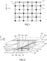
- qubit matrices are produced, for example from silicon, in the form of a two-dimensional matrix 1 as shown in the figure. figure 1 .
- the white circles referenced 10 represent data qubits and the black circles referenced 12 represent measurement qubits.
- the neighboring qubits 10, 12 are interconnected to each other by tunnel barriers 14.
- the data qubits 10 are staggered with respect to each other, and the measurement qubits 12 are staggered. in relation to each other.
- These qubits 10, 12 are aligned and arranged forming rows and columns.
- each data qubit 10 is linked to two (for a data qubit 10 lying in a corner of the matrix), three (for a data qubit 10 lying on an edge of the matrix) or four (for all other data qubits 10 that are neither in a corner nor on an edge of the matrix) measure qubits 12, and that each measure qubit 12 is linked to two (for a qubit measure 12 lying in a corner of the matrix), three (for a measure qubit 12 lying on one edge of the matrix) or four (for all other measure qubits 12 not in a corner or on one edge of the matrix) data qubits 10.
- each of the measurement qubits 12 must be coupled to a detection element (not shown on the figure 1 ) the operation of which is comparable to that of a single electron transistor or "Single Electron Transistor" (SET), making it possible to detect whether or not a load is present on the qubit to which the detection element is coupled.
- This detection element must also be able to be used to send or receive a charge carrier (electron or a hole) from or to at least one of the measurement qubits 12 (and if possible also on at least one of the data qubits 10).
- a first problem which arises with such a matrix 1 of qubits concerns the addressing of the qubits 10, 12 which must be carried out in such a structure. Indeed, each of the measurement qubits 12, and possibly each of the data qubits 10, must be connected to an electrical connection forming an electrical access to this qubit from outside the matrix 1.
- a matrix of qubits 3 x 3 no qubits arranged in a square of three rows and three columns
- making the electrical connections for addressing to each of these nine qubits requires at least two levels of electrical interconnections: a first level for the central qubit of this matrix and a second level for the other qubits located around this central qubit.
- a second problem posed by such a matrix 1 relates to the production of the detection elements to be coupled to the qubits. Indeed, given the dimensions sought for the realization of the qubits (two neighboring qubits being for example spaced from one another by a distance of between about 5 nm and 100 nm, and each qubit has lateral dimensions, for example example a diameter, included between approximately 5 nm and 100 nm), the production of these detection elements within this matrix 1 of qubits is difficult to envisage.
- a third problem posed by such a matrix 1 is that, as for the realization of the addressing of the qubits, the realization of the addressing of the detection elements is problematic because of the large number of electrical connections to be made.
- An aim of the present invention is to provide a quantum device with qubits of spins in which the addressing of qubits arranged by forming a two-dimensional matrix is carried out with a reduced number of levels of electrical interconnections.
- the present invention provides a quantum device with qubits of spins according to independent claim 1.
- the control of an individual qubit can come from the row and column addressing of the tunnel barriers (for example two, three or four depending on the disposition of the qubit addressed within the matrix) connected to this qubit and controlled. by the electrostatic grids formed opposite these tunnel barriers.
- the tunnel barriers can be formed by portions of semiconductor narrower than those forming the qubits. Such narrower semiconductor portions are called "constrictions”.
- Each data qubit can be linked to at least two neighboring measurement qubits and each measurement qubit can be linked to at least two neighboring data qubits.
- Each of the first electrically conductive portions can be connected to the first ends of the first conductive vias, the second ends of which are arranged opposite the first tunnel barriers connecting data qubits and measurement qubits arranged on two neighboring columns of the first matrix, and each second electrically conductive portions can be connected to the first ends of the second conductive vias, the second ends of which are arranged opposite the second tunnel barriers connecting data qubits and measurement qubits arranged on two neighboring lines of the first matrix.
- the quantum device may further comprise a second semiconductor layer comprising a second matrix of charge detectors, each comprising for example a quantum dot (or “quantum dot”), each of the measurement qubits. electrically connectable to one of the charge detectors by a first semiconductor portion extending between the first and second semiconductor layers, each of the first semiconductor portions being able to be coupled to at least one gate capable of , or configured to, control a tunnel coupling between the charge detector and the measurement qubit connected by said first portion of semiconductor.
- each of the first gates controls the electrical conduction within one of the first portions of semiconductor which each connects one of the measurement qubits to one of the charge detectors.
- the charge detectors are realized within a semiconductor level different from that in which the data qubits and the measurement qubits are located.
- Such a configuration solves the problems of density of realization of the qubits encountered in the structures of the prior art, and therefore makes it possible to carry out the data qubits and the measurement qubits with small dimensions (two neighboring qubits being for example spaced apart the each other by a distance of between about 5 nm and 100 nm, and each qubit having lateral dimensions, for example a diameter, of between about 5 nm and 100 nm).
- the constraints associated with the production of the second matrix of charge detectors are also reduced.
- the first and second gates can be coating and each be arranged around one of the first semiconductor portions.
- the quantum device may further include a second semiconductor layer and a second array of charge detectors formed by second semiconductor portions extending between the first and second semiconductor layers. conductor, each of said second semiconductor portions being connectable by at least a third tunnel barrier with at least one of the measurement qubits arranged, in the plane of the first semiconductor layer, around said second semiconductor portion.
- the second One embodiment proposes to realize the charge detectors using the second semiconductor portions which extend between the first and second semiconductor layers.
- the addressing of the charge detectors is not carried out by means of the first and second gates formed around the first portions of semiconductor, but by means of the means for addressing the qubits. data and measurement qubits which also make it possible to act on the conduction of the third tunnel barriers which connect the charge detectors at least to the measurement qubits.
- This second embodiment has the advantage of not having to make coating gates between the two semiconductor layers.
- each of the second semiconductor portions can be connected by at least two third tunnel barriers to at least two measurement qubits arranged in the plane of the first semiconductor layer, around said second semiconductor portion.
- the quantum device according to this configuration has the advantage of reducing the number of charge detectors used by pooling the charge detectors for at least several measurement qubits.
- each of the data qubits can be linked to one of the load detectors.
- first and second gates For these first semiconductor portions connecting the charge detectors to the data qubits, it is possible for the first and second gates to be coating and each disposed around one of these first semiconductor portions.
- each of said second semiconductor portions when each of the data qubits is connected to one of the charge detectors, each of said second semiconductor portions is connected by at least one third tunnel barrier to at least one of the measurement or data qubits. arranged, in the plane of the first semiconductor layer, around said second semiconductor portion.
- each of the second semiconductor portions can be connected by four third tunnel barriers to at least two measurement qubits and two data qubits arranged, in the plane of the first semiconductor layer, around said second portion semiconductor.
- the first semiconductor layer can be disposed between the second semiconductor layer and the first and second metallization levels.
- the second semiconductor layer may further include doped portions capable of, or configured to, form charge carrier reservoirs. to which the load detectors are connected via fourth tunnel barriers.
- each of the doped portions can be connected to several charge detectors arranged on the same row or the same column of the second matrix. This pooling of the portions doped with several charge detectors is advantageous because it is not necessary to carry out an individual control of the fourth tunnel barriers.
- the quantum device may further include second gates capable of, or configured to, control by field effect the conduction of each of the fourth tunnel barriers.
- the second gates can be formed by fifth electrically conductive portions extending parallel to the rows or columns of the first matrix, arranged facing the fourth tunnel barriers and spaced from the fourth tunnel barriers by a second dielectric layer. Further, the fifth electrically conductive portions may be formed in a conductive level such that the second semiconductor layer is disposed between the first semiconductor layer and the conductive level.
- Each of the fifth electrically conductive portions can form several second gates.
- the invention also relates to a method according to independent claim 14.
- the quantum device 100 comprises spin qubits arranged in a matrix of the “coded surface” type as previously described in connection with the figure 1 .
- the spin qubits are produced within a semiconductor layer 102, for example silicon.
- the reference 104 designates the data qubits and the reference 106 designates the measurement qubits.
- Each of the qubits 104, 106 has lateral dimensions (in the (X, Y) plane), for example a diameter or a side, between approximately 5 nm and 100 nm, and advantageously equal to approximately 40 nm, and a thickness per example between about 5 nm and 30 nm.
- the distance between two neighboring qubits 104, 106 arranged on the same row or the same column of the matrix is for example between approximately 5 nm and 100 nm, and advantageously of the order of 40 nm.
- the data qubits 104 are staggered relative to one another, and the measurement qubits 106 are staggered relative to one another.
- These qubits 104, 106 are arranged by forming rows and columns of the matrix.
- the qubits 104, 106 are arranged such that each data qubit 104 is linked to two (when the qubit is in a corner of the matrix), three (when the qubit is at an edge of the matrix ) or four (for other qubits that are not in a corner or at an edge of the matrix) measure qubits 106, and that likewise, each measure qubit 106 be connected to two, three or four qubits of data 104.
- the qubits 104, 106 are interconnected to each other by tunnel barriers 108 corresponding to portions of semiconductor of the layer 102.
- the spacing of two neighboring qubits arranged on the same row or the same column of the matrix corresponds to the length of one of the tunnel barriers 108.
- the semiconductor portions forming the tunnel barriers 108 have for example a thickness similar to those forming the qubits 104, 106, that is to say between approximately 5 nm and 30 nm. nm, and have a width less than the lateral dimensions (for example the diameter) of the qubits 104, 106, for example between about 5 nm and 40 nm.
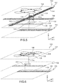
- the figure 2 corresponds to a schematic perspective view of part of the device 100, in which only two data qubits 104 and two measurement qubits 106 are represented.
- the figure 3 corresponds to a schematic top view of part of the device 100, on which a 3 x 3 matrix formed of five data qubits 104 and four measurement qubits 106 is shown.
- the semiconductor layer 102 in which the qubits 104, 106 are made is covered with a dielectric layer 111 and a dielectric material 110.
- Two levels of metallizations are formed within this dielectric material 110.
- a first of two levels, referenced 112 is arranged between the semiconductor layer 102 and a second of the two levels, referenced 114.
- the dielectric material 110 is for example SiO 2 , or advantageously a dielectric material having a dielectric constant of lower value than that of SiO 2 (so-called “Low-k” material), such as for example SiOCH or porous SiO 2.
- first conductive portions 116 form longitudinal portions extending in a first direction, that is to say having their largest dimension substantially parallel to this first direction. This first direction is substantially parallel to the rows or to the columns of the qubit matrix 104, 106.
- the first conductive portions 116 extend parallel to the Y axis, that is to say parallel to the columns of the qubit matrix 104, 106 shown in these figures.
- Each of the first conductive portions 116 extends opposite the tunnel barriers 108 connecting the qubits 104, 106 forming two adjacent columns of the matrix.
- the first level of metallizations 112 comprises (n-1) first conductive portions 116 each extending above the tunnel barriers 108 connecting the qubits 104, 106 belonging to two neighboring columns of the matrix.
- First electrically conductive vias 118 are made in the part of the dielectric material 110 located between the first level of metallizations 112 and the dielectric layer 111. Like the first conductive portions 116, these first vias 118 are arranged opposite the tunnel barriers 108 which each connect two neighboring qubits 104, 106 belonging to two neighboring columns.
- the first vias 118 each comprise a first end 120 electrically connected to one of the first conductive portions 116, and a second end 122 close to one of the tunnel barriers 108 but such that the dielectric layer 111 is present between this second end 122 and said tunnel barrier 108.
- the thickness of this dielectric layer 111 is for example between approximately 2 nm and 20 nm.
- the material of the dielectric layer 111 is such that it advantageously comprises a dielectric constant greater than that of SiO 2 (so-called “High-k” material), and corresponds for example to an SiO 2 / HfO 2 , SiO 2 / nitride bilayer. silicon, or contains SiCO.
- second conductive portions 124 form longitudinal portions extending in a second direction substantially perpendicular to the first direction of the first conductive portions 116.
- the second conductive portions 124 extend parallel to the X axis, that is to say parallel to the lines of the matrix of qubits 104, 106 shown in these figures.
- Each of the second conductive portions 124 extends opposite the tunnel barriers 108 connecting the qubits 104, 106 forming two neighboring lines of the matrix.
- the second level of metallizations 114 comprises (n-1) second conductive portions 124 each extending above the tunnel barriers 108 connecting the qubits 104, 106 belonging to two neighboring rows of the matrix.
- Second electrically conductive vias 126 are made in the part of the dielectric material 110 located between the second level of metallizations 114 and the dielectric layer 111. Like the second conductive portions 124, these second vias 126 are arranged opposite the tunnel barriers 108 which each connect two neighboring qubits 104, 106 belonging to two neighboring lines.
- the second vias 126 each comprise a first end 128 electrically connected to one of the second conductive portions 124, and a second end 130 close to one of the tunnel barriers 108 but such that the dielectric layer 111 is present between this second end 130 and said tunnel barrier 108 .
- the addressing of the qubits 104 and 106 is not carried out by means of electrical connections each connected directly to one of the qubits 104, 106, but by the intermediary of the conductive portions 116, 124 and conductive vias 118, 126 which make it possible to control the location of the qubit addressed via the field effect control of the conduction within the tunnel barriers 108, in a manner analogous to the gates of field effect transistors.
- the conductive portions 116, 124 and the conductive vias 118, 126 can therefore be seen as forming gates controlling the electrical conduction of the tunnel links between the qubits 104, 106.
- the electrical potential within the data qubit 104 located at the center of the matrix shown is controlled by means of the two first conductive portions 116 and the two second conductive portions 124 visible in this figure and which are adjacent (top view ) to this qubit 104, and by the first and second conductive vias 118, 126 arranged above the tunnel barriers 108 connecting this data qubit 104 to the four measurement qubits 106 located around this data qubit 104.
- each of the conductive portions 116, 124 makes it possible to act on n tunnel barriers 108, and therefore on the electrical potentials of 2n qubits 104, 106 (those connected by said n tunnel barriers 108).
- n tunnel barriers 108 Whatever the value of n, only two metallization levels make it possible to address all the qubits of a matrix of n x n qubits.
- 2 (n-1) conductive portions and 2n (n-1) conductive vias therefore make it possible to individually address each of the qubits of the matrix.
- each conductive via acts on a tunnel barrier 108 connecting two qubits 104, 106, it is possible to simultaneously address individually at most n (n-1) qubits.
- the device 100 also comprises a second semiconductor layer 132 in which are made charge detectors 134 intended to perform a detection of charges and also to exchange charges (electrons or holes) with the qubits 104, 106.
- charge detectors 134 have physical characteristics (size, spacing, materials, etc.) similar to those of the data qubits 104 and the qubits of measure 106.
- the first semiconductor layer 102 is disposed between the second semiconductor layer 132 and the first level of metallizations 112.
- Another dielectric layer 133 is interposed between the first semiconductor layer 102 and the second semiconductor layer. driver 132.
- Each charge detector 134 is formed by a portion of the second semiconductor layer 132, of dimensions for example similar to those of the qubits 104, 106.
- Each charge detector 134 has for example a section, in the plane of the second. semiconductor layer 132, of substantially circular shape with a diameter equal to approximately 40 nm.
- Two neighboring charge detectors 134 are for example spaced from one another by a distance of between approximately 5 nm and 100 nm, for example of the order of 40 nm.
- At least each measurement qubit 106, and possibly each data qubit 104, is connected to one of the charge detectors 134 arranged opposite this qubit 104, 106.
- the connections between the measurement qubits 106 (and possibly the data qubits 104) and the charge detectors 134 are formed by portions of semiconductor 136 forming pillars extending between the layers 102 and 132, in the dielectric layer 133.
- the number of charge detectors 134 made in the second layer 132 and the number of semiconductor portions 136 are therefore each equal to the number of measurement qubits 106 produced in the first layer 102 when the charge detectors 134 are only connected to the measurement qubits 106, and are each equal to the number total of qubits 104, 106 when the load detectors 134 are connected to the measurement qubits 106 and to the data qubits 104.
- a single charge detector 134 and a single semiconductor portion 136 are shown.
- the load sensors 134 are arranged at a second matrix similar to the first matrix formed by the qubits 104, 106 and the device 100 therefore comprises n 2 or n 2/2 detectors load 134 (in the case of an nxn matrix of qubits 104, 106).
- Each charge detector 134 is connected to a reservoir of charge carriers (electrons or holes) making it possible to supply charge carriers to the charge detectors 134, then to the qubits 106 and possibly 104.
- the charge detectors 134 arranged on the same row or on the same column of the second matrix of charge detectors 134 are connected to the same doped portion 138 of the second semiconductor layer 132 extending parallel to this row or this column of charge detectors 134.
- the doped portions 138 extend parallel to the X axis, that is to say parallel to the lines of the matrix of charge detectors 134.
- the doped portions 138 may extend parallel to the axis Y, that is to say parallel to the columns of the matrix of charge detectors 134.
- the charge detectors 134 are connected to the doped portions 138 by tunnel barriers 140.
- These tunnel barriers 140 are for example of a similar nature to the tunnel barriers 108 connecting the qubits 104, 106 to each other, that is to say formed by portions of semiconductor of dimensions and shape such that they form tunnel barriers.
- the passage of the charge carriers between the measurement qubits 106, or possibly the data qubits 104, and the charge detectors 134 is controlled by grids 142 each formed around the portions 136.
- a first gate 142a and a second gate 142b are formed by portions of conductive material surrounding one of the portions 136, a dielectric material 166 being present between this portion 136 and this conductive gate material.
- These gates 142a, 142b have an operation similar to that of a gate of a transistor and control the passage of the charge carriers in the portions 136, between one of the charge detectors 134 and one of the data qubits or measuring 104, 106, electrostatically and as a function of the electric potential applied to them.
- the addressing of the gates 142a, 142b is carried out by using third longitudinal conductive portions 144 which extend in a direction parallel to the rows or columns of the qubit matrix 104, 106 (in parallel with the columns on the example of figure 5 , that is to say parallel to the Y axis), and to fourth longitudinal conductive portions 146 extending in a direction perpendicular to that of the third conductive portions 144 (parallel to the X axis on the figure 5 ).
- each of the portions 136 is surrounded by two grids 142a, 142b formed by two separate conductive portions spaced apart from one another.
- the first grid 142a is connected to one of the third conductive portions 144 and the second grid 142b is connected to one of the fourth conductive portions 146.
- Each of the third and fourth conductive portions 144, 146 is connected to one of the two grids 142a, 142b formed around each of the portions 136 arranged on the same row or the same column.
- the third conductive portion 144 shown is electrically connected to the first grid 142a shown as well as to the other first grids 142a located on the column to which the first grid 142a shown belongs.
- the fourth conductive portion 146 shown is electrically connected to the second grid 142b shown as well as to the other second grids 142b located on the line to which the second grid 142b shown belongs.
- the passage of the charge carriers in one of the portions 136 is controlled by applying suitable electrical potentials to the third conductive portion 144 and to the fourth conductive portion 146 which are connected to the first and second gates 142a, 142b which surround this portion 136.
- the third and fourth conductive portions 144, 146 are disposed in the dielectric layer 133.
- fifth conductive portions 148 are formed within a conductive level 150 disposed under the second semiconductor layer 132. It is not necessary that the tunnel barriers 140 be addressed individually, but it is possible. Each of these fifth conductive portions 148 can simultaneously control the conductivity of a set of tunnel barriers 140, for example all the tunnel barriers 140 associated with the charge detectors 134 located on the same line, as is the case on the figure 5 , or on the same column. These fifth conductive portions 148 comprise for example at least one metal and / or polycrystalline silicon.
- Another dielectric layer 152 is interposed between the conductive level 150 and the second semiconductor layer 132.
- This dielectric layer 152 comprises for example a dielectric with high permittivity (“High-k”) or an oxide.
- the conductive level 150 is based on a holding assembly comprising a dielectric layer 153, comprising for example oxide, and a support layer 154, for example a solid layer, or “bulk”, of semiconductor.
- the thickness of this dielectric layer 152 is thin enough, for example between about 2 nm and 25 nm so that the fifth conductive portions 148 control the tunnel barriers 140 electrostatically, in a manner analogous to a transistor gate. For this, the fifth conductive portions 148 are arranged opposite the tunnel barriers 140.
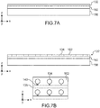
- the figure 6 schematically represents a part of the quantum device 100 according to a second embodiment.
- each charge detector 134 is formed by a portion of semiconductor extending between the two layers of semiconductors 102, 132.
- each load detector 134 is here common to several measurement qubits 106 , and possibly common to several measurement qubits 106 and data qubits 104.
- each load detector 134 is common to four qubits 104, 106 arranged to form a 2 x 2 matrix and which, seen from above, are disposed around the load sensor 134.
- the device 100 therefore comprises a number of load sensors 134 equal to n 2/4.
- tunnel barriers 108 connecting the qubits 104, 106 to each other
- other portions of semiconductor of the layer 102 form tunnel barriers 156 connecting each of the charge detectors 134 to each of the data and measurement qubits 104, 106 associated with this load detector 134.
- the load detectors 134 can only be connected to the measurement qubits 106.
- each load detector 134 can be connected to two measurement qubits 106 via two tunnel barriers 156.
- each charge detector 134 is connected to a reservoir of charge carriers making it possible to supply charge carriers to the charge detectors 134, formed by a doped portion 138 of the semiconductor layer 132.
- the charge detectors 134 are connected to the doped portions 138 by the tunnel barriers 140 which, as in the first embodiment, are controlled by the fifth conductive portions 148 formed within the conductive level 150.
- these tunnel barriers 156 are here controlled by a tunnel coupling modulated via the first and second conductive portions 116, 126 which act indirectly on these links 156.
- the gates formed by the portions 116, 126 can "push" the wave function of the load of the qubit in question towards the load detector 134, which is equivalent to lowering the tunnel barrier 156.
- These grids can also move away this wave function and thus increase the level of the tunnel barrier 156.
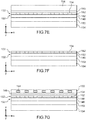
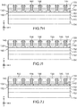
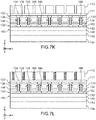
- a method of making the quantum device 100 according to a particular embodiment is now described in connection with the figures 7A to 7L .
- the device 100 is made from an SOI substrate comprising a solid semiconductor layer 158, for example of silicon, a buried dielectric layer 160, for example of SiO 2 , and a surface layer of semiconductor, by example of silicon, corresponding to the second semiconductor layer 132 ( figure 7A ).
- the thickness of the second semiconductor layer 132 is for example between approximately 5 nm and 30 nm.
- the second semiconductor layer 132 is etched such that the remaining portions of this layer form the charge detectors 134 spaced from one another.
- the charge detectors 134 are produced in the form of portions of a semiconductor section, in the plane of the layer 132 (plane (X, Y)), of substantially circular shape.
- Other remaining portions 138 of this semiconductor layer, present between the charge detectors 134, are doped in order to form reservoirs of charge carriers.
- other remaining portions of this semiconductor layer form the fourth tunnel barriers 140.
- a dielectric material 162 is then deposited in order to fill the spaces formed in the layer 132, between the charge detectors 134, the portions 138 and the tunnel barriers 140. Planarization is implemented in order to eliminate the dielectric material 162 deposited, thus forming an electrical insulation around these elements.
- the conductor level 150 is then carried out. For this, a stack of layers comprising the dielectric layer 152 and an electrically conductive layer, for example metallic or comprising doped polysilicon, is produced on the detection elements 134 and the dielectric material 162. The electrically conductive layer is then etched with stop. on the dielectric layer 152 in order to form the fifth conductive portions 148 intended to control the passage of the charge carriers in the tunnel barriers 140 intended to connect the charge detectors 134 to the doped portions 138 ( figure 7C ).
- an electrically conductive layer for example metallic or comprising doped polysilicon
- a dielectric material for example semiconductor oxide, is then deposited on the conductive level 150, and in particular between the fifth conductive portions 148, then planarized to form portions insulating the fifth conductive portions 148 as well as the dielectric layer. 153 ( figure 7D ).
- the assembly is then turned over and secured to the support layer 154 intended for the mechanical retention of the assembly ( figure 7E ).
- the layers 158 and 160 of the initial substrate are then removed, revealing the rear face of the second semiconductor layer 132, and making the charge detectors 134 accessible ( figure 7F ).
- the conductive portions 144 and 146 as well as the gates 142 are then produced by the implementation of several steps of depositing and etching conductive materials (for example polysilicon or metal gate material such as TiN or tungsten), and several intermediate deposits of a dielectric material and planarizations (or deposits of a planarizing oxide of the HSQ type, or hydrogen-silsesquioxane) to form the dielectric layer 133 ( figure 7G ).
- the thickness of the assembly formed of the conductive portions 144, 146 and of the dielectric layer 133 is for example between approximately 5 nm and 20 nm.
- Vias 164 are then made through the dielectric layer 133 and the conductive materials of the portions 144, 146 and of the gates 142 in order to form the locations of the semiconductor portions 136. These vias 164 are made by the implementation of an etching with stop on the semiconductor of the layer 132.
- Dielectric material for example a semiconductor oxide such as SiO 2 or semiconductor nitride, is then deposited, in particular by covering the side walls of vias 164. Anisotropic etching is then carried out in order to preserve only parts 166 of this dielectric material disposed against the side walls of vias 164 ( figure 7H ). These parts of dielectric material 166 are intended to form the gate dielectrics between the gates 142 and the semiconductor portions 136.
- a semiconductor oxide such as SiO 2 or semiconductor nitride
- the production of the portions 136 also includes the implementation of a mechanical-chemical planarization with stopping on the dielectric layer 133 in order to remove the semi. -conductor obtained by growth lying outside vias 164 ( figure 7I ).
- the semiconductor layer 102 is then formed on the upper face of the assembly formed by the dielectric layer 133, the semiconductor portions 136 and the parts 166 of this dielectric material, for example via a hydrophobic or hydrophilic direct bonding ( figure 7J ).
- the data and measurement qubits 104, 106 are then formed in the semiconductor layer 102 by etching.
- the dielectric layer 111 is then produced, then a part of the dielectric material 110, for example SiO 2 , is also produced on the dielectric layer 111. Vias 168 are then produced through the dielectric material 110, the dielectric layer 111 being by example likely to serve as a stop layer for this etching ( figure 7K ).
- the dielectric layer 111 comprises, for example, nitride or a silicon oxide / nitride bilayer such as nitride, serving as a stop material, can then be etched at the end of the etching used to produce vias 118, 126.
- Conductive material is then deposited in vias 168, forming conductive vias 118 ( figure 7L ).
- the metallization levels 112, 114 are completed by successively implementing a step of depositing and etching a conductive material to form the conductive portions 116, then the deposition and etching of another part of the dielectric material 110 for the production of vias 126, and finally steps of depositing and etching a conductive material to form conductive portions 124.
Landscapes
- Engineering & Computer Science (AREA)
- Physics & Mathematics (AREA)
- Theoretical Computer Science (AREA)
- General Physics & Mathematics (AREA)
- Data Mining & Analysis (AREA)
- Computing Systems (AREA)
- Evolutionary Computation (AREA)
- Computational Mathematics (AREA)
- Mathematical Analysis (AREA)
- Mathematical Optimization (AREA)
- Pure & Applied Mathematics (AREA)
- Condensed Matter Physics & Semiconductors (AREA)
- General Engineering & Computer Science (AREA)
- Mathematical Physics (AREA)
- Software Systems (AREA)
- Artificial Intelligence (AREA)
- Photometry And Measurement Of Optical Pulse Characteristics (AREA)
- Thin Film Transistor (AREA)
- Non-Volatile Memory (AREA)
- Semiconductor Memories (AREA)
Claims (14)
- Quantenvorrichtung (100) mit Spin-Qubits, zumindest enthaltend:- eine erste Halbleiterschicht (102) mit einer ersten Matrix von Daten-Qubits (104) und Maß-Qubits (106), die über Tunnelbarrieren (108) miteinander verbunden sind;- Mittel zum Adressieren der Daten-Qubits (104) und der Maß-Qubits (106), die dazu ausgelegt sind, die Leitung jeder der Tunnelbarrieren (108) durch Feldeffekt zu steuern, und die zumindest enthalten:• erste und zweite elektrisch leitende Abschnitte (116, 124), die jeweils in einer ersten bzw. zweiten darüber liegenden Metallisierungsebene (112, 114) angeordnet sind;• erste und zweite elektrisch leitende Durchkontaktierungen (118, 126), die jeweils ein erstes Ende (120, 128) aufweisen, das mit einem der ersten bzw. zweiten elektrisch leitenden Abschnitte (118, 126) verbunden ist, sowie ein zweites Ende (122, 130), das einer der Tunnelbarrieren (108) gegenüberliegend angeordnet ist;- eine erste dielektrische Schicht (111), die zwischen den Tunnelbarrieren (108) und den zweiten Enden (122, 130) der ersten bzw. zweiten elektrisch leitenden Durchkontaktierungen (118, 126) eingefügt ist;
und ferner enthaltend:- in einer ersten Konfiguration eine zweite Halbleiterschicht (132), die eine zweite Matrix von Ladungsdetektoren (134) aufweist, wobei jedes der Maß-Qubits (106) über einen ersten Halbleiterabschnitt (136), der sich zwischen der ersten und der zweiten Halbleiterschicht (102, 132) erstreckt, mit einem der Ladungsdetektoren (134) elektrisch verbunden ist, wobei jeder der ersten Halbleiterabschnitte (136) mit zumindest einem Gatter (142a, 142b) gekoppelt ist, das dazu ausgelegt ist, eine Tunnelkopplung zwischen dem Ladungsdetektor (134) und dem Maß-Qubit (106) zu steuern, die über den ersten Halbleiterabschnitt (136) verbunden sind, oder- in einer zweiten Konfiguration eine zweite Halbleiterschicht (132) und eine zweite Matrix von Ladungsdetektoren (134), die aus zweiten Halbleiterabschnitten gebildet sind, die sich zwischen der ersten und der zweiten Halbleiterschicht (102, 132) erstrecken, wobei jeder der zweiten Halbleiterabschnitte über zumindest eine dritte Tunnelbarriere (156) mit zumindest einem der Maß-Qubits (106) verbunden ist, die in der Ebene der ersten Halbleiterschicht (102) um den zweiten Halbleiterabschnitt herum angeordnet sind. - Quantenvorrichtung (100) nach Anspruch 1, wobei:- in der ersten Matrix die Daten-Qubits (104) und die Maß-Qubits (106) entlang einer ersten und einer dazu senkrechten zweiten Richtung ausgerichtet sind und Zeilen und Spalten der ersten Matrix bilden;- die zweiten Enden (122) der ersten elektrisch leitenden Durchkontaktierungen (118) einem Teil der Tunnelbarrieren (108), erste Tunnelbarrieren (108) genannt, gegenüberliegend angeordnet sind, die jeweils eines der Daten-Qubits (104) und eines der benachbarten Maß-Qubits (106) verbinden und auf derselben Zeile der ersten Matrix angeordnet sind;- die zweiten Enden (130) der zweiten elektrisch leitenden Durchkontaktierungen (126) einem weiteren Teil der Tunnelbarrieren (108), zweite Tunnelbarrieren (108) genannt, gegenüberliegend angeordnet sind, die jeweils eines der Daten-Qubits (104) und eines der benachbarten Maß-Qubits (106) verbinden und auf derselben Spalte der ersten Matrix angeordnet sind.
- Quantenvorrichtung (100) nach Anspruch 2, wobei jeder der ersten elektrisch leitenden Abschnitte (116) mit den ersten Enden (120) der ersten leitenden Durchkontaktierungen (118) verbunden ist, deren zweite Enden (122) den ersten Tunnelbarrieren (108) gegenüberliegend angeordnet sind, die Daten-Qubits (104) und Maß-Qubits (106) verbinden, die auf zwei benachbarten Spalten der ersten Matrix angeordnet sind, und wobei jeder der zweiten elektrisch leitenden Abschnitte (124) mit den ersten Enden (128) der zweiten leitenden Durchkontaktierungen (126) verbunden ist, deren zweite Enden (130) den zweiten Tunnelbarrieren (108) gegenüberliegend angeordnet sind, die Daten-Qubits (104) und Maß-Qubits (106) verbinden, die auf zwei benachbarten Zeilen der ersten Matrix angeordnet sind.
- Quantenvorrichtung (100) nach Anspruch 2, wobei sich die Quantenvorrichtung (100) in einer ersten Konfiguration befindet und jeder der ersten Halbleiterabschnitte (136) mit einem ersten Gatter (142a) und einem zweiten Gatter (142b) gekoppelt ist, die dazu ausgelegt sind, eine Tunnelkopplung zwischen dem Ladungsdetektor (134) und dem Maß-Qubit (106) zu steuern, die über den ersten Halbleiterabschnitt (136) verbunden sind, und die voneinander getrennt und beabstandet sind, und wobei die Quantenvorrichtung (100) ferner enthält:- dritte elektrisch leitende Abschnitte (144), die jeweils mit den ersten Gattern (142a) verbunden sind, die um die ersten Halbleiterabschnitte (136) herum angeordnet sind, die zumindest mit den Maß-Qubits (106) verbunden sind, die auf derselben Spalte der ersten Matrix angeordnet sind;- vierte elektrisch leitende Abschnitte (146), die jeweils mit den zweiten Gattern (142b) verbunden sind, die um die ersten Halbleiterabschnitte (136) herum angeordnet sind, die zumindest mit den Maß-Qubits (106) verbunden sind, die auf derselben Zeile der ersten Matrix angeordnet sind.
- Quantenvorrichtung (100) nach Anspruch 4, wobei das erste und das zweite Gatter (142a, 142b) als Umhüllung ausgebildet sind und jeweils um einen der ersten Halbleiterabschnitte (136) herum angeordnet sind.
- Quantenvorrichtung (100) nach einem der Ansprüche 1 bis 3, wobei die Quantenvorrichtung (100) sich in der zweiten Konfiguration befindet und jeder der zweiten Halbleiterabschnitte über zumindest zwei dritte Tunnelbarrieren (156) mit zumindest zwei Maß-Qubits (106) verbunden ist, die in der Ebene der ersten Halbleiterschicht um den zweiten Halbleiterabschnitt herum angeordnet sind.
- Quantenvorrichtung (100) nach einem der vorangehenden Ansprüche, wobei jedes der Daten-Qubits (104) mit einem der Ladungsdetektoren (134) verbunden ist.
- Quantenvorrichtung (100) nach einem der vorangehenden Ansprüche, wobei die erste Halbleiterschicht (102) zwischen der zweiten Halbleiterschicht (132) und der ersten und zweiten Metallisierungsebene (112, 114) angeordnet ist.
- Quantenvorrichtung (100) nach einem der vorangehenden Ansprüche, wobei die zweite Halbleiterschicht (132) ferner dotierte Abschnitte (138) aufweist, die dazu ausgelegt sind, Ladungsträgerreservoirs zu bilden, mit denen die Ladungsdetektoren (134) über vierte Tunnelbarrieren (140) verbunden sind.
- Quantenvorrichtung (100) nach Anspruch 9, wobei jeder der dotierten Abschnitte (138) mit mehreren Ladungsdetektoren (134) verbunden ist, die in derselben Zeile bzw. derselben Spalte der zweiten Matrix angeordnet sind.
- Quantenvorrichtung (100) nach einem der Ansprüche 9 oder 10, ferner enthaltend zweite Gatter, die dazu ausgelegt sind, die Leitung jeder der vierten Tunnelbarrieren (140) durch Feldeffekt zu steuern.
- Quantenvorrichtung (100) nach Anspruch 11, wobei die zweiten Gatter aus fünften elektrisch leitenden Abschnitten (148) gebildet sind, die sich parallel zu den Zeilen bzw. Spalten der ersten Matrix erstrecken, den vierten Tunnelbarrieren (140) gegenüberliegend angeordnet sind und von den vierten Tunnelbarrieren (140) durch eine zweite dielektrische Schicht (152) beabstandet sind.
- Quantenvorrichtung (100) nach Anspruch 12, wobei die fünften elektrisch leitenden Abschnitte (148) in einer leitenden Ebene (150) ausgebildet sind, so dass die zweite Halbleiterschicht (132) zwischen der ersten Halbleiterschicht (102) und der leitenden Ebene (150) angeordnet ist.
- Verfahren zur Herstellung einer Quantenvorrichtung (100) mit Spin-Qubits, das zumindest die folgenden Schritte umfasst:- Ausbilden einer ersten Matrix von Daten-Qubits (104) und Maß-Qubits (106), die über Tunnelbarrieren (108) miteinander verbunden sind, in einer ersten Halbleiterschicht (102);- Ausbilden einer ersten dielektrischen Schicht (111) auf der ersten Halbleiterschicht (102); und- Ausbilden von ersten und zweiten elektrisch leitenden Abschnitten (116, 124), die jeweils in einer ersten bzw. einer zweiten darüber liegenden Metallisierungsebene (112, 114) angeordnet sind;- Ausbilden von ersten und zweiten elektrisch leitenden Durchkontaktierungen (118, 126), die jeweils ein erstes Ende (120, 128), das mit einem der ersten bzw. zweiten elektrisch leitenden Abschnitte (118, 126) verbunden ist, und ein zweites Ende (122, 130) aufweisen, das einer der Tunnelbarrieren (108) gegenüberliegend angeordnet ist, so dass die erste dielektrische Schicht (111) zwischen den Tunnelbarrieren (108) und den zweiten Enden (122, 130) der ersten und zweiten elektrisch leitenden Durchkontaktierungen (118, 126) eingefügt ist;
und das ferner umfasst:- in einer ersten Konfiguration Ausbilden einer zweiten Matrix von Ladungsdetektoren (134) in einer zweiten Halbleiterschicht (132), wobei jedes der Maß-Qubits (106) über einen ersten Halbleiterabschnitt (136), der sich zwischen der ersten und der zweiten Halbleiterschicht (102, 132) erstreckt, mit einem der Ladungsdetektoren (134) elektrisch verbunden ist, wobei jeder der ersten Halbleiterabschnitte (136) mit zumindest einem Gatter (142a, 142b) gekoppelt ist, das dazu ausgelegt ist, eine Tunnelkopplung zwischen dem Ladungsdetektor (134) und dem Maß-Qubit (106) zu steuern, die über den ersten Halbleiterabschnitt (136) verbunden sind, oder- in einer zweiten Konfiguration Ausbilden einer zweiten Matrix von Ladungsdetektoren (134), die aus zweiten Halbleiterabschnitten gebildet sind, die sich zwischen der ersten Halbleiterschicht (102) und einer zweiten Halbleiterschicht (132) erstrecken, wobei jeder der zweiten Halbleiterabschnitte über zumindest eine dritte Tunnelbarriere (156) mit zumindest einem der Maß-Qubits (106) verbunden ist, die in der Ebene der ersten Halbleiterschicht (102) um den zweiten Halbleiterabschnitt herum angeordnet sind.
Applications Claiming Priority (1)
| Application Number | Priority Date | Filing Date | Title |
|---|---|---|---|
| FR1754156A FR3066297B1 (fr) | 2017-05-11 | 2017-05-11 | Dispositif quantique a qubits de spin |
Publications (2)
| Publication Number | Publication Date |
|---|---|
| EP3401848A1 EP3401848A1 (de) | 2018-11-14 |
| EP3401848B1 true EP3401848B1 (de) | 2021-07-28 |
Family
ID=59811432
Family Applications (1)
| Application Number | Title | Priority Date | Filing Date |
|---|---|---|---|
| EP18171613.5A Active EP3401848B1 (de) | 2017-05-11 | 2018-05-09 | Quantenvorrichtung mit spin-qubits |
Country Status (4)
| Country | Link |
|---|---|
| US (1) | US10607993B2 (de) |
| EP (1) | EP3401848B1 (de) |
| CN (1) | CN108878519B (de) |
| FR (1) | FR3066297B1 (de) |
Cited By (2)
| Publication number | Priority date | Publication date | Assignee | Title |
|---|---|---|---|---|
| FR3155634A1 (fr) * | 2023-11-21 | 2025-05-23 | Commissariat A L'energie Atomique Et Aux Energies Alternatives | Dispositif quantique et procédé de fabrication associé |
| WO2025259110A1 (en) * | 2024-06-13 | 2025-12-18 | Technische Universiteit Delft | Quantum dot device with mirror-symmetrically arranged quantum dot units |
Families Citing this family (21)
| Publication number | Priority date | Publication date | Assignee | Title |
|---|---|---|---|---|
| GB201906936D0 (en) * | 2019-05-16 | 2019-07-03 | Quantum Motion Tech Limited | Processor element for quantum information processor |
| DE102019120716A1 (de) * | 2019-07-31 | 2021-02-04 | Universität Leipzig | Verfahren und Vorrichtung zur Adressierung von Qubits sowie Verfahren zur Herstellung der Vorrichtung |
| US11417819B2 (en) * | 2020-04-27 | 2022-08-16 | Microsoft Technology Licensing, Llc | Forming a bumpless superconductor device by bonding two substrates via a dielectric layer |
| FR3116946B1 (fr) | 2020-11-27 | 2022-11-11 | Commissariat Energie Atomique | Procédé de réalisation d’un dispositif quantique |
| FR3118023B1 (fr) | 2020-12-23 | 2023-01-27 | Commissariat Energie Atomique | Procédé de lecture de l’état de spin d’un système et procédé de détermination de la fidélité associé |
| FR3118022B1 (fr) | 2020-12-23 | 2023-02-10 | Commissariat Energie Atomique | Procédé de détermination de la position du régime totalement isolé d’un qubit de spin et procédé de manipulation d’au moins un qubits de spin |
| NL2028581B1 (en) * | 2021-06-29 | 2023-01-09 | Univ Delft Tech | An addressable quantum dot array |
| NL2028580B1 (en) * | 2021-06-29 | 2023-01-09 | Univ Delft Tech | Quantum dot structures comprising an integrated single electron tunneling readout and single electron tunneling quantum dot readout structures |
| NL2028596B1 (en) | 2021-06-30 | 2023-01-10 | Univ Delft Tech | Controlling uniformity of an array of quantum dots |
| FR3126521B1 (fr) * | 2021-08-31 | 2023-09-01 | Commissariat Energie Atomique | Dispositif quantique, procédé de lecture de l’état de charge, procédé de détermination d’un diagramme de stabilité et procédé de détermination des corrélations de spin |
| FR3127831B1 (fr) | 2021-10-01 | 2023-10-20 | Commissariat Energie Atomique | Procédé de fabrication d'un circuit électronique quantique |
| FR3128313A1 (fr) | 2021-10-14 | 2023-04-21 | Commissariat A L'energie Atomique Et Aux Energies Alternatives | Matrice de boîtes quantiques à qubits de spin |
| FR3143797B1 (fr) * | 2022-12-14 | 2026-01-16 | Commissariat Energie Atomique | Electrodes d'échange pour réseau d’ilots quantiques |
| FR3143799B1 (fr) | 2022-12-20 | 2025-05-23 | Commissariat A L Energie Atomique Et Aux Energies Alternatives | Dispositif quantique destiné à former une matrice de boites quantiques et procédé de fabrication associé |
| FR3143798B1 (fr) | 2022-12-20 | 2025-12-12 | Commissariat Energie Atomique | Dispositif quantique destiné à former une matrice de boites quantiques et procédé de fabrication associé |
| FR3147031B1 (fr) | 2023-03-22 | 2025-03-21 | Commissariat Energie Atomique | Circuit électronique quantique et procédé de fabrication associé |
| FR3155609A1 (fr) | 2023-11-21 | 2025-05-23 | Commissariat A L'energie Atomique Et Aux Energies Alternatives | Dispositif quantique à matrice bidimensionnelle et son procédé de réalisation |
| FR3155631A1 (fr) | 2023-11-21 | 2025-05-23 | Commissariat A L'energie Atomique Et Aux Energies Alternatives | Dispositif quantique et procédé de fabrication associé |
| FR3155608B1 (fr) | 2023-11-21 | 2025-11-28 | Commissariat Energie Atomique | Dispositif a structure de detection a blocage de coulomb superposee a une boite quantique |
| FR3155949A1 (fr) | 2023-11-24 | 2025-05-30 | Commissariat A L'energie Atomique Et Aux Energies Alternatives | Realisation de motifs dans une couche mince au moyen d’un masque dur doublement implante |
| FR3161295A1 (fr) | 2024-04-10 | 2025-10-17 | Commissariat A L'energie Atomique Et Aux Energies Alternatives | Dispositif a matrice de boites quantiques et de regions de couplage |
Family Cites Families (11)
| Publication number | Priority date | Publication date | Assignee | Title |
|---|---|---|---|---|
| DE69418143T2 (de) * | 1993-11-02 | 1999-08-26 | Matsushita Electric Industrial Co. | Verfahren zur Herstellung eines Aggregats von Mikro-Nadeln aus Halbleitermaterial |
| DE19746138A1 (de) * | 1997-10-18 | 1999-04-22 | Siemens Ag | Verfahren zum Detektieren eines Stroms spingpolarsierter Elektronen in einem Festkörper |
| GB0021302D0 (en) * | 2000-08-30 | 2000-10-18 | Scient Generics Ltd | Spin filter device |
| US20020152191A1 (en) * | 2001-02-23 | 2002-10-17 | Hollenberg Lloyd Christopher Leonard | Method of interrogating a database using a quantum computer |
| EP1262911A1 (de) * | 2001-05-30 | 2002-12-04 | Hitachi Europe Limited | Quantenrechner |
| CN100585629C (zh) * | 2004-12-23 | 2010-01-27 | D-波系统公司 | 包括量子装置的模拟处理器 |
| US8648426B2 (en) * | 2010-12-17 | 2014-02-11 | Seagate Technology Llc | Tunneling transistors |
| US9842921B2 (en) * | 2013-03-14 | 2017-12-12 | Wisconsin Alumni Research Foundation | Direct tunnel barrier control gates in a two-dimensional electronic system |
| US10229365B2 (en) * | 2014-11-03 | 2019-03-12 | Newsouth Innovations Pty Limited | Apparatus and method for quantum processing |
| US10068181B1 (en) * | 2015-04-27 | 2018-09-04 | Rigetti & Co, Inc. | Microwave integrated quantum circuits with cap wafer and methods for making the same |
| US9985193B2 (en) * | 2015-06-30 | 2018-05-29 | International Business Machines Corporation | Architecture for coupling quantum bits using localized resonators |
-
2017
- 2017-05-11 FR FR1754156A patent/FR3066297B1/fr active Active
-
2018
- 2018-05-01 US US15/967,778 patent/US10607993B2/en active Active
- 2018-05-09 EP EP18171613.5A patent/EP3401848B1/de active Active
- 2018-05-10 CN CN201810445082.9A patent/CN108878519B/zh active Active
Non-Patent Citations (1)
| Title |
|---|
| None * |
Cited By (3)
| Publication number | Priority date | Publication date | Assignee | Title |
|---|---|---|---|---|
| FR3155634A1 (fr) * | 2023-11-21 | 2025-05-23 | Commissariat A L'energie Atomique Et Aux Energies Alternatives | Dispositif quantique et procédé de fabrication associé |
| EP4561295A1 (de) * | 2023-11-21 | 2025-05-28 | Commissariat à l'Energie Atomique et aux Energies Alternatives | Zweidimenionale quantenvorrichtungsmatrix mit integrierten ladungsdetektoren und verfahren zur herstellung |
| WO2025259110A1 (en) * | 2024-06-13 | 2025-12-18 | Technische Universiteit Delft | Quantum dot device with mirror-symmetrically arranged quantum dot units |
Also Published As
| Publication number | Publication date |
|---|---|
| CN108878519B (zh) | 2024-02-20 |
| US10607993B2 (en) | 2020-03-31 |
| CN108878519A (zh) | 2018-11-23 |
| US20180331108A1 (en) | 2018-11-15 |
| FR3066297B1 (fr) | 2019-06-14 |
| EP3401848A1 (de) | 2018-11-14 |
| FR3066297A1 (fr) | 2018-11-16 |
Similar Documents
| Publication | Publication Date | Title |
|---|---|---|
| EP3401848B1 (de) | Quantenvorrichtung mit spin-qubits | |
| FR3086456A1 (fr) | Procede de realisation de transistors superposes | |
| EP1993138B1 (de) | Transistorvorrichtung mit verspanntem Kanal | |
| EP3701567B1 (de) | Verfahren zur herstellung eines elektronischen bauteils mit doppelquantenpunkten | |
| EP4092750B1 (de) | 1t1r-speicher mit 3d-struktur | |
| FR3078441A1 (fr) | Dispositif quantique comprenant des transistors fet et des qubits co-integres sur un meme substrat | |
| FR3033665A1 (fr) | Transistor a electron unique et son procede de realisation | |
| FR3120740A1 (fr) | Dispositif à deux niveaux de grilles de commande électrostatique superposés | |
| EP4561295A1 (de) | Zweidimenionale quantenvorrichtungsmatrix mit integrierten ladungsdetektoren und verfahren zur herstellung | |
| FR3118961A1 (fr) | Dispositif comprenant des grilles de commande électrostatique reparties sur deux faces opposées d’une portion de semi-conducteur | |
| EP4391068A1 (de) | Quantenvorrichtung zur formung einer quantenpunktmatrix und herstellungsverfahren dafür | |
| EP4167290A1 (de) | Spin-qubit-quantentopfmatrix | |
| EP1677347B1 (de) | Magnetischer Speicher | |
| EP4125141A1 (de) | Phasenwechselspeicher | |
| FR3083001A1 (fr) | Capteur d'images | |
| EP4086822B1 (de) | Vorrichtung mit elementen zur kompensation der lokalen variabilität des elektrostatischen potenzials | |
| FR3126063A1 (fr) | Dispositif pour le stockage, le contrôle et la manipulation de l’information quantique (qubits) sur semi-conducteur | |
| EP3361498B1 (de) | Entkopplungskondensator | |
| FR3118288A1 (fr) | Integration d'un circuit de detection a base de resonateurs optiques interconnectes sur un circuit de lecteure d'un imageur | |
| EP1586118B1 (de) | Vergrabener kondensator für eine sram-speicherzelle | |
| EP4561293A1 (de) | Quantenvorrichtungen, bestehend aus einer matrix von quantenboxen und integrierten ladungsdetektoren, sowie verfahren zur herstellung dieser vorrichtungen | |
| EP4633324A1 (de) | Quantenpunkt-matrix-vorrichtung mit kopplungsbereiche, mit gates auf gegenüberliegenden seiten der quantenpunkt-matrix | |
| EP4554353A1 (de) | Spin qubit vorrichtung mit quantenpunkten, die in einem nanodraht durch gates gebildet werden | |
| FR3125915A1 (fr) | Procede de gravure selective isotrope de silicium | |
| FR3155358A1 (fr) | Procédé de fabrication d’un circuit électronique quantique avec un pas de grille réduit |
Legal Events
| Date | Code | Title | Description |
|---|---|---|---|
| PUAI | Public reference made under article 153(3) epc to a published international application that has entered the european phase |
Free format text: ORIGINAL CODE: 0009012 |
|
| STAA | Information on the status of an ep patent application or granted ep patent |
Free format text: STATUS: REQUEST FOR EXAMINATION WAS MADE |
|
| 17P | Request for examination filed |
Effective date: 20180511 |
|
| AK | Designated contracting states |
Kind code of ref document: A1 Designated state(s): AL AT BE BG CH CY CZ DE DK EE ES FI FR GB GR HR HU IE IS IT LI LT LU LV MC MK MT NL NO PL PT RO RS SE SI SK SM TR |
|
| AX | Request for extension of the european patent |
Extension state: BA ME |
|
| STAA | Information on the status of an ep patent application or granted ep patent |
Free format text: STATUS: EXAMINATION IS IN PROGRESS |
|
| 17Q | First examination report despatched |
Effective date: 20200207 |
|
| REG | Reference to a national code |
Ref country code: DE Ref legal event code: R079 Ref document number: 602018020666 Country of ref document: DE Free format text: PREVIOUS MAIN CLASS: G06N0099000000 Ipc: G06N0010000000 |
|
| GRAP | Despatch of communication of intention to grant a patent |
Free format text: ORIGINAL CODE: EPIDOSNIGR1 |
|
| STAA | Information on the status of an ep patent application or granted ep patent |
Free format text: STATUS: GRANT OF PATENT IS INTENDED |
|
| RIC1 | Information provided on ipc code assigned before grant |
Ipc: H01L 29/66 20060101ALI20210211BHEP Ipc: G06N 10/00 20190101AFI20210211BHEP |
|
| INTG | Intention to grant announced |
Effective date: 20210226 |
|
| RAP1 | Party data changed (applicant data changed or rights of an application transferred) |
Owner name: COMMISSARIAT A L'ENERGIE ATOMIQUE ET AUX ENERGIES ALTERNATIVES Owner name: CENTRE NATIONAL DE LA RECHERCHE SCIENTIFIQUE |
|
| GRAS | Grant fee paid |
Free format text: ORIGINAL CODE: EPIDOSNIGR3 |
|
| GRAA | (expected) grant |
Free format text: ORIGINAL CODE: 0009210 |
|
| STAA | Information on the status of an ep patent application or granted ep patent |
Free format text: STATUS: THE PATENT HAS BEEN GRANTED |
|
| AK | Designated contracting states |
Kind code of ref document: B1 Designated state(s): AL AT BE BG CH CY CZ DE DK EE ES FI FR GB GR HR HU IE IS IT LI LT LU LV MC MK MT NL NO PL PT RO RS SE SI SK SM TR |
|
| REG | Reference to a national code |
Ref country code: GB Ref legal event code: FG4D Free format text: NOT ENGLISH |
|
| REG | Reference to a national code |
Ref country code: CH Ref legal event code: EP |
|
| REG | Reference to a national code |
Ref country code: AT Ref legal event code: REF Ref document number: 1415379 Country of ref document: AT Kind code of ref document: T Effective date: 20210815 |
|
| REG | Reference to a national code |
Ref country code: IE Ref legal event code: FG4D Free format text: LANGUAGE OF EP DOCUMENT: FRENCH |
|
| REG | Reference to a national code |
Ref country code: DE Ref legal event code: R096 Ref document number: 602018020666 Country of ref document: DE |
|
| REG | Reference to a national code |
Ref country code: LT Ref legal event code: MG9D |
|
| REG | Reference to a national code |
Ref country code: NL Ref legal event code: MP Effective date: 20210728 |
|
| REG | Reference to a national code |
Ref country code: AT Ref legal event code: MK05 Ref document number: 1415379 Country of ref document: AT Kind code of ref document: T Effective date: 20210728 |
|
| PG25 | Lapsed in a contracting state [announced via postgrant information from national office to epo] |
Ref country code: ES Free format text: LAPSE BECAUSE OF FAILURE TO SUBMIT A TRANSLATION OF THE DESCRIPTION OR TO PAY THE FEE WITHIN THE PRESCRIBED TIME-LIMIT Effective date: 20210728 Ref country code: FI Free format text: LAPSE BECAUSE OF FAILURE TO SUBMIT A TRANSLATION OF THE DESCRIPTION OR TO PAY THE FEE WITHIN THE PRESCRIBED TIME-LIMIT Effective date: 20210728 Ref country code: HR Free format text: LAPSE BECAUSE OF FAILURE TO SUBMIT A TRANSLATION OF THE DESCRIPTION OR TO PAY THE FEE WITHIN THE PRESCRIBED TIME-LIMIT Effective date: 20210728 Ref country code: RS Free format text: LAPSE BECAUSE OF FAILURE TO SUBMIT A TRANSLATION OF THE DESCRIPTION OR TO PAY THE FEE WITHIN THE PRESCRIBED TIME-LIMIT Effective date: 20210728 Ref country code: SE Free format text: LAPSE BECAUSE OF FAILURE TO SUBMIT A TRANSLATION OF THE DESCRIPTION OR TO PAY THE FEE WITHIN THE PRESCRIBED TIME-LIMIT Effective date: 20210728 Ref country code: NL Free format text: LAPSE BECAUSE OF FAILURE TO SUBMIT A TRANSLATION OF THE DESCRIPTION OR TO PAY THE FEE WITHIN THE PRESCRIBED TIME-LIMIT Effective date: 20210728 Ref country code: NO Free format text: LAPSE BECAUSE OF FAILURE TO SUBMIT A TRANSLATION OF THE DESCRIPTION OR TO PAY THE FEE WITHIN THE PRESCRIBED TIME-LIMIT Effective date: 20211028 Ref country code: PT Free format text: LAPSE BECAUSE OF FAILURE TO SUBMIT A TRANSLATION OF THE DESCRIPTION OR TO PAY THE FEE WITHIN THE PRESCRIBED TIME-LIMIT Effective date: 20211129 Ref country code: AT Free format text: LAPSE BECAUSE OF FAILURE TO SUBMIT A TRANSLATION OF THE DESCRIPTION OR TO PAY THE FEE WITHIN THE PRESCRIBED TIME-LIMIT Effective date: 20210728 Ref country code: BG Free format text: LAPSE BECAUSE OF FAILURE TO SUBMIT A TRANSLATION OF THE DESCRIPTION OR TO PAY THE FEE WITHIN THE PRESCRIBED TIME-LIMIT Effective date: 20211028 Ref country code: LT Free format text: LAPSE BECAUSE OF FAILURE TO SUBMIT A TRANSLATION OF THE DESCRIPTION OR TO PAY THE FEE WITHIN THE PRESCRIBED TIME-LIMIT Effective date: 20210728 |
|
| PG25 | Lapsed in a contracting state [announced via postgrant information from national office to epo] |
Ref country code: PL Free format text: LAPSE BECAUSE OF FAILURE TO SUBMIT A TRANSLATION OF THE DESCRIPTION OR TO PAY THE FEE WITHIN THE PRESCRIBED TIME-LIMIT Effective date: 20210728 Ref country code: LV Free format text: LAPSE BECAUSE OF FAILURE TO SUBMIT A TRANSLATION OF THE DESCRIPTION OR TO PAY THE FEE WITHIN THE PRESCRIBED TIME-LIMIT Effective date: 20210728 Ref country code: GR Free format text: LAPSE BECAUSE OF FAILURE TO SUBMIT A TRANSLATION OF THE DESCRIPTION OR TO PAY THE FEE WITHIN THE PRESCRIBED TIME-LIMIT Effective date: 20211029 |
|
| PG25 | Lapsed in a contracting state [announced via postgrant information from national office to epo] |
Ref country code: DK Free format text: LAPSE BECAUSE OF FAILURE TO SUBMIT A TRANSLATION OF THE DESCRIPTION OR TO PAY THE FEE WITHIN THE PRESCRIBED TIME-LIMIT Effective date: 20210728 |
|
| REG | Reference to a national code |
Ref country code: DE Ref legal event code: R097 Ref document number: 602018020666 Country of ref document: DE |
|
| PG25 | Lapsed in a contracting state [announced via postgrant information from national office to epo] |
Ref country code: SM Free format text: LAPSE BECAUSE OF FAILURE TO SUBMIT A TRANSLATION OF THE DESCRIPTION OR TO PAY THE FEE WITHIN THE PRESCRIBED TIME-LIMIT Effective date: 20210728 Ref country code: SK Free format text: LAPSE BECAUSE OF FAILURE TO SUBMIT A TRANSLATION OF THE DESCRIPTION OR TO PAY THE FEE WITHIN THE PRESCRIBED TIME-LIMIT Effective date: 20210728 Ref country code: RO Free format text: LAPSE BECAUSE OF FAILURE TO SUBMIT A TRANSLATION OF THE DESCRIPTION OR TO PAY THE FEE WITHIN THE PRESCRIBED TIME-LIMIT Effective date: 20210728 Ref country code: EE Free format text: LAPSE BECAUSE OF FAILURE TO SUBMIT A TRANSLATION OF THE DESCRIPTION OR TO PAY THE FEE WITHIN THE PRESCRIBED TIME-LIMIT Effective date: 20210728 Ref country code: CZ Free format text: LAPSE BECAUSE OF FAILURE TO SUBMIT A TRANSLATION OF THE DESCRIPTION OR TO PAY THE FEE WITHIN THE PRESCRIBED TIME-LIMIT Effective date: 20210728 Ref country code: AL Free format text: LAPSE BECAUSE OF FAILURE TO SUBMIT A TRANSLATION OF THE DESCRIPTION OR TO PAY THE FEE WITHIN THE PRESCRIBED TIME-LIMIT Effective date: 20210728 |
|
| PLBE | No opposition filed within time limit |
Free format text: ORIGINAL CODE: 0009261 |
|
| STAA | Information on the status of an ep patent application or granted ep patent |
Free format text: STATUS: NO OPPOSITION FILED WITHIN TIME LIMIT |
|
| 26N | No opposition filed |
Effective date: 20220429 |
|
| PG25 | Lapsed in a contracting state [announced via postgrant information from national office to epo] |
Ref country code: IT Free format text: LAPSE BECAUSE OF FAILURE TO SUBMIT A TRANSLATION OF THE DESCRIPTION OR TO PAY THE FEE WITHIN THE PRESCRIBED TIME-LIMIT Effective date: 20210728 |
|
| REG | Reference to a national code |
Ref country code: CH Ref legal event code: PL |
|
| PG25 | Lapsed in a contracting state [announced via postgrant information from national office to epo] |
Ref country code: MC Free format text: LAPSE BECAUSE OF FAILURE TO SUBMIT A TRANSLATION OF THE DESCRIPTION OR TO PAY THE FEE WITHIN THE PRESCRIBED TIME-LIMIT Effective date: 20210728 Ref country code: LU Free format text: LAPSE BECAUSE OF NON-PAYMENT OF DUE FEES Effective date: 20220509 Ref country code: LI Free format text: LAPSE BECAUSE OF NON-PAYMENT OF DUE FEES Effective date: 20220531 Ref country code: CH Free format text: LAPSE BECAUSE OF NON-PAYMENT OF DUE FEES Effective date: 20220531 |
|
| PG25 | Lapsed in a contracting state [announced via postgrant information from national office to epo] |
Ref country code: IE Free format text: LAPSE BECAUSE OF NON-PAYMENT OF DUE FEES Effective date: 20220509 |
|
| PG25 | Lapsed in a contracting state [announced via postgrant information from national office to epo] |
Ref country code: HU Free format text: LAPSE BECAUSE OF FAILURE TO SUBMIT A TRANSLATION OF THE DESCRIPTION OR TO PAY THE FEE WITHIN THE PRESCRIBED TIME-LIMIT; INVALID AB INITIO Effective date: 20180509 |
|
| PG25 | Lapsed in a contracting state [announced via postgrant information from national office to epo] |
Ref country code: MK Free format text: LAPSE BECAUSE OF FAILURE TO SUBMIT A TRANSLATION OF THE DESCRIPTION OR TO PAY THE FEE WITHIN THE PRESCRIBED TIME-LIMIT Effective date: 20210728 Ref country code: CY Free format text: LAPSE BECAUSE OF FAILURE TO SUBMIT A TRANSLATION OF THE DESCRIPTION OR TO PAY THE FEE WITHIN THE PRESCRIBED TIME-LIMIT Effective date: 20210728 |
|
| PG25 | Lapsed in a contracting state [announced via postgrant information from national office to epo] |
Ref country code: MT Free format text: LAPSE BECAUSE OF FAILURE TO SUBMIT A TRANSLATION OF THE DESCRIPTION OR TO PAY THE FEE WITHIN THE PRESCRIBED TIME-LIMIT Effective date: 20210728 |
|
| PGFP | Annual fee paid to national office [announced via postgrant information from national office to epo] |
Ref country code: DE Payment date: 20250519 Year of fee payment: 8 |
|
| PGFP | Annual fee paid to national office [announced via postgrant information from national office to epo] |
Ref country code: GB Payment date: 20250527 Year of fee payment: 8 |
|
| PGFP | Annual fee paid to national office [announced via postgrant information from national office to epo] |
Ref country code: BE Payment date: 20250523 Year of fee payment: 8 |
|
| PGFP | Annual fee paid to national office [announced via postgrant information from national office to epo] |
Ref country code: FR Payment date: 20250526 Year of fee payment: 8 |
|
| PG25 | Lapsed in a contracting state [announced via postgrant information from national office to epo] |
Ref country code: TR Free format text: LAPSE BECAUSE OF FAILURE TO SUBMIT A TRANSLATION OF THE DESCRIPTION OR TO PAY THE FEE WITHIN THE PRESCRIBED TIME-LIMIT Effective date: 20210728 |