EP4561295A1 - Zweidimenionale quantenvorrichtungsmatrix mit integrierten ladungsdetektoren und verfahren zur herstellung - Google Patents
Zweidimenionale quantenvorrichtungsmatrix mit integrierten ladungsdetektoren und verfahren zur herstellung Download PDFInfo
- Publication number
- EP4561295A1 EP4561295A1 EP24214630.6A EP24214630A EP4561295A1 EP 4561295 A1 EP4561295 A1 EP 4561295A1 EP 24214630 A EP24214630 A EP 24214630A EP 4561295 A1 EP4561295 A1 EP 4561295A1
- Authority
- EP
- European Patent Office
- Prior art keywords
- grid
- dielectric
- grids
- layer
- charge
- Prior art date
- Legal status (The legal status is an assumption and is not a legal conclusion. Google has not performed a legal analysis and makes no representation as to the accuracy of the status listed.)
- Pending
Links
Images









Classifications
-
- H—ELECTRICITY
- H10—SEMICONDUCTOR DEVICES; ELECTRIC SOLID-STATE DEVICES NOT OTHERWISE PROVIDED FOR
- H10N—ELECTRIC SOLID-STATE DEVICES NOT OTHERWISE PROVIDED FOR
- H10N60/00—Superconducting devices
- H10N60/10—Junction-based devices
- H10N60/128—Junction-based devices having three or more electrodes, e.g. transistor-like structures
-
- G—PHYSICS
- G06—COMPUTING OR CALCULATING; COUNTING
- G06N—COMPUTING ARRANGEMENTS BASED ON SPECIFIC COMPUTATIONAL MODELS
- G06N10/00—Quantum computing, i.e. information processing based on quantum-mechanical phenomena
- G06N10/40—Physical realisations or architectures of quantum processors or components for manipulating qubits, e.g. qubit coupling or qubit control
-
- H—ELECTRICITY
- H10—SEMICONDUCTOR DEVICES; ELECTRIC SOLID-STATE DEVICES NOT OTHERWISE PROVIDED FOR
- H10D—INORGANIC ELECTRIC SEMICONDUCTOR DEVICES
- H10D30/00—Field-effect transistors [FET]
- H10D30/40—FETs having zero-dimensional [0D], one-dimensional [1D] or two-dimensional [2D] charge carrier gas channels
- H10D30/402—Single electron transistors; Coulomb blockade transistors
-
- H—ELECTRICITY
- H10—SEMICONDUCTOR DEVICES; ELECTRIC SOLID-STATE DEVICES NOT OTHERWISE PROVIDED FOR
- H10D—INORGANIC ELECTRIC SEMICONDUCTOR DEVICES
- H10D48/00—Individual devices not covered by groups H10D1/00 - H10D44/00
- H10D48/01—Manufacture or treatment
- H10D48/031—Manufacture or treatment of three-or-more electrode devices
-
- H—ELECTRICITY
- H10—SEMICONDUCTOR DEVICES; ELECTRIC SOLID-STATE DEVICES NOT OTHERWISE PROVIDED FOR
- H10D—INORGANIC ELECTRIC SEMICONDUCTOR DEVICES
- H10D48/00—Individual devices not covered by groups H10D1/00 - H10D44/00
- H10D48/383—Quantum effect devices, e.g. of devices using quantum reflection, diffraction or interference effects
- H10D48/3835—Semiconductor qubit devices comprising a plurality of quantum mechanically interacting semiconductor quantum dots, e.g. Loss-DiVincenzo spin qubits
-
- H—ELECTRICITY
- H10—SEMICONDUCTOR DEVICES; ELECTRIC SOLID-STATE DEVICES NOT OTHERWISE PROVIDED FOR
- H10D—INORGANIC ELECTRIC SEMICONDUCTOR DEVICES
- H10D62/00—Semiconductor bodies, or regions thereof, of devices having potential barriers
- H10D62/10—Shapes, relative sizes or dispositions of the regions of the semiconductor bodies; Shapes of the semiconductor bodies
- H10D62/117—Shapes of semiconductor bodies
- H10D62/118—Nanostructure semiconductor bodies
-
- H—ELECTRICITY
- H10—SEMICONDUCTOR DEVICES; ELECTRIC SOLID-STATE DEVICES NOT OTHERWISE PROVIDED FOR
- H10D—INORGANIC ELECTRIC SEMICONDUCTOR DEVICES
- H10D62/00—Semiconductor bodies, or regions thereof, of devices having potential barriers
- H10D62/80—Semiconductor bodies, or regions thereof, of devices having potential barriers characterised by the materials
- H10D62/81—Semiconductor bodies, or regions thereof, of devices having potential barriers characterised by the materials of structures exhibiting quantum-confinement effects, e.g. single quantum wells; of structures having periodic or quasi-periodic potential variation
- H10D62/812—Single quantum well structures
- H10D62/814—Quantum box structures
-
- H—ELECTRICITY
- H10—SEMICONDUCTOR DEVICES; ELECTRIC SOLID-STATE DEVICES NOT OTHERWISE PROVIDED FOR
- H10D—INORGANIC ELECTRIC SEMICONDUCTOR DEVICES
- H10D64/00—Electrodes of devices having potential barriers
- H10D64/20—Electrodes characterised by their shapes, relative sizes or dispositions
- H10D64/27—Electrodes not carrying the current to be rectified, amplified, oscillated or switched, e.g. gates
-
- H—ELECTRICITY
- H10—SEMICONDUCTOR DEVICES; ELECTRIC SOLID-STATE DEVICES NOT OTHERWISE PROVIDED FOR
- H10N—ELECTRIC SOLID-STATE DEVICES NOT OTHERWISE PROVIDED FOR
- H10N60/00—Superconducting devices
- H10N60/01—Manufacture or treatment
-
- H—ELECTRICITY
- H10—SEMICONDUCTOR DEVICES; ELECTRIC SOLID-STATE DEVICES NOT OTHERWISE PROVIDED FOR
- H10N—ELECTRIC SOLID-STATE DEVICES NOT OTHERWISE PROVIDED FOR
- H10N60/00—Superconducting devices
- H10N60/10—Junction-based devices
- H10N60/11—Single-electron tunnelling devices
-
- B—PERFORMING OPERATIONS; TRANSPORTING
- B82—NANOTECHNOLOGY
- B82Y—SPECIFIC USES OR APPLICATIONS OF NANOSTRUCTURES; MEASUREMENT OR ANALYSIS OF NANOSTRUCTURES; MANUFACTURE OR TREATMENT OF NANOSTRUCTURES
- B82Y10/00—Nanotechnology for information processing, storage or transmission, e.g. quantum computing or single electron logic
Definitions
- the technical field of the invention is that of quantum electronics and more particularly quantum electronic devices and their manufacture.
- Quantum dots Semiconductor technologies capable of manipulating qubits include islands, also called quantum dots, made in nanometric confinement structures defined, for example, electrostatically within a semiconductor layer. Quantum dots ensure the confinement of elementary charges, electrons or holes, and quantum information is, for example, encoded on the spin of these particles.
- a quantum box For a quantum box to be functional, that is to say for it to be able to be initialized, manipulated and read, it must be coupled to reading electronics capable of determining the number of charges in the quantum box.
- SETs Single Electron Transistors
- a SET consists of a quantum dot, or island, two charge reservoirs, also called drain and source, and a gate contact.
- the island is connected to each of the tanks by at least one tunnel junction, or tunnel coupling, defined electrostatically.
- the charge reservoirs are considered as bulk metallic materials whose electrons obey Fermi-Dirac statistics, and the island is for example a metal grain whose size is a few nanometers.
- the gate contact is typically a layer of dielectric material.
- the tunnel junction is realized by another layer of dielectric material, called tunnel junction, arranged so as to separate the island from the charge reservoirs and the gate contact.
- One or more electrodes are further connected to the charge reservoirs and the gate contact to apply a voltage to these elements.
- the operation of SETs is based on a capacitive coupling with the quantum dot, a fluctuation in the number of charges of the quantum dot modifying for example the conduction of the SET and can therefore be measured.
- This detection, or reading, of the resulting charge is generally carried out by current (in transport) or by reflectometry with the use of an LC resonator.
- the SET When the SET is read in current, its drain and source are biased independently of each other. In other words, two independent charge reservoirs (source and drain) are required.
- the SET When the SET is read by reflectometry, it does not need to be crossed by a static current. Its drain and source are therefore polarizable at the same potential, and a single charge reservoir (drain or source) is sufficient. In this case, the SET, which is no longer quite equivalent to a transistor, is also called a “single-lead quantum dot" or SLQD (for "Single Lead Quantum Dot” according to the commonly used acronym).
- SLQD Single Lead Quantum Dot
- Integrating SETs closer to the qubits would be advantageous for improving detection sensitivity and preserving the space needed to implement qubit control functionalities.
- the patent application FR 3 066 297 thus proposes a parallel-controlled quantum electronic circuit comprising a semiconductor layer receiving a matrix of qubits, a network of electrodes arranged on each side of this semiconductor layer, and a plane stacked on the semiconductor layer comprising a matrix of charge detectors.
- the architecture of this circuit is particularly complex, particularly due to the high density of vias and interconnections. As a result, certain manufacturing steps can be difficult to carry out.
- the present invention provides a solution to the problems mentioned above by making it possible to reduce, on the electronic chip, the size and complexity of charge detectors read by reflectometry.
- the conductive island of each charge detector is formed at the same level as that of the first and second grids (the expression "same level” here means in the level between a lower face of the first grids and an upper face of the second grids).
- the conductive island which is placed on the dielectric in a two-dimensional mesh, there is a good capacitive coupling between the quantum dot formed directly above the two-dimensional mesh and the neighboring quantum dots. This proximity improves the detection sensitivity of the quantum device. It should be added that forming the conductive islands between first grids offers the advantage of being able to use these first grids as an alignment marker during the manufacturing steps of the conductive islands. In other words, the first grids allow the islands to be "self-aligned”. This self-alignment facilitates these manufacturing steps.
- the quantum device according to the invention thus offers an integration solution compatible with industrial manufacturing processes and the integration of quantum dots on a large scale, while allowing the required proximity between the charge detectors read in current and the quantum dots.
- the predetermined angle is such that the barrier strips are oriented at 45° relative to the direction of the first grids, the barrier strips extending, in the direction perpendicular to the first grids, over four adjacent conductive strips.
- the present invention is placed in the context of quantum electronic devices and their manufacturing method. More particularly, the invention aims to enable, via charge detectors read by reflectometry, efficient detection of the charge state of the quantum dots formed on the quantum devices. In particular, again, the invention aims to reduce the space occupied by these charge detectors on the quantum device to provide an architecture making it possible to produce large-scale spin qubits.
- THE figures 1 , 2 , 3 and 4 represent, in a schematic form, a quantum device 100 according to a first embodiment
- FIG. 1 shows, in schematic form, a top view of a part of the quantum device 100 according to this first embodiment.
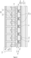
- THE figures 2 to 4 show different views of a first variant embodiment of the quantum device 100 shown in the Figure 1 .
- THE figures 5 to 6 show different views of a second alternative embodiment of the quantum device 100 shown in the Figure 1 .
- the quantum device 100 extends in a plane ⁇ X,Y ⁇ and is formed from a semiconductor layer 110.
- the device 100 further comprises a dielectric 121, first and second gates 131, 132 and charge detectors 140.
- the first gates and the second gates are coupling gates.
- the terms “thickness” or “height” designate dimensions measured perpendicular to the plane ⁇ X; Y ⁇ .
- the expression “lateral dimension” designates a dimension measured in the plane ⁇ X; Y ⁇ .
- grid may be used herein to refer to a line of grids.
- a "line of grids” means a line comprising a plurality of grids.
- the grids overlying an area between two quantum dots are grids controlling the potential barriers between the two quantum dots in question.
- the semiconductor layer 110 has a front face 110a, illustrated in Figure 2 .
- the semiconductor layer 110 is adapted to form a matrix of quantum dots.
- the semiconductor layer 110 has characteristics allowing a matrix 115 of quantum dots 1151 to be formed within it. These quantum dots are represented by hatched circles on the Figure 1 .
- matrix here refers to an arrangement of quantum dots in rows 115a and columns 115b.
- the semiconductor layer 110 has a thickness of between 5 nm and 35 nm and preferably between 10 nm and 20 nm, for example equal to 15 nm.
- the semiconductor layer 110 is preferably a silicon layer 110.
- this silicon layer 110 comes from a substrate 10 of the silicon on insulator or SOI type (acronym for “Silicon On insulator” in English).
- Such a substrate 10 is notably illustrated in the Figure 2 . It comprises a stack, from bottom to top, of a massive semiconductor layer 105, an insulating layer 107, and the silicon semiconductor layer 110.
- the insulating layer 107 is arranged between the massive semiconductor layer 105 and the semiconductor layer 110.
- the polarization of such a substrate 10 makes it possible to electrostatically control charge confinements in the semiconductor layer 110.
- the semiconductor layer 110 may, alternatively, be a bulk silicon layer.
- the semiconductor layer 110 may, alternatively, be a semiconductor heterostructure comprising a quantum well or a two-dimensional electron gas (2DEG). Such structures have interfaces with low defect densities, facilitating charge confinement and electrostatic control.
- 2DEG two-dimensional electron gas
- the semiconductor layer 110 can advantageously have holes 117. These holes 117 are illustrated by white circles on the Figure 1 These holes 117 can for example be obtained by etching the semiconductor layer 110.
- the holes 117 are preferentially arranged in rows and columns to form a matrix of holes 117.
- the lines of holes 117 are oriented in a first direction X corresponding to the direction of the lines 115a of quantum dots 1151.
- the columns of holes 117 are oriented in a second direction Y corresponding to the direction of the columns 115b of quantum dots 1151.
- the holes 117 are arranged between the rows and columns of quantum dots. Preferably, four holes 115 frame each zone corresponding to a quantum dot 1151.
- the diameter of the holes 117 is preferably between 20 nm and 50 nm.
- the holes 117 structure the semiconductor layer 110 to confine charges in each non-etched zone, that is to say in the zone corresponding to the quantum dot 1151. The presence of the holes 117 thus facilitates the formation of the quantum dots 1151.
- the dielectric 121 is arranged on the front face 110a of the semiconductor layer 110 and is formed of one or more layers, each layer being formed of a dielectric material (cf. Figure 2 Or Figure 6 ).
- the dielectric 121 consists of a single layer 120 of dielectric which covers the front face 110a of the semiconductor layer 110.
- the layer 120 of dielectric has a thickness preferably between 5 nm and 10 nm and is electrically insulating.
- the layer 120 of dielectric is for example made of silicon oxide (SiO2).
- the dielectric layer 120 is covered, between the first grids 131, by another dielectric layer, called spacer layer 133 (on the Figure 2 , these portions of spacer layer 133 arranged on the dielectric layer 120 are denoted 133 D ).
- the dielectric 121 is the stack consisting of the dielectric layer 120 and the spacer layer 133 D arranged on this dielectric layer 120.
- This variant embodiment is easier to produce than the variant in which the dielectric 121 consists of the dielectric layer 120 only. Indeed, it is then not necessary to structure the spacer layer 133, once it has been deposited on the first gates 131 and the dielectric layer 120.
- This variant therefore makes it possible to avoid an anisotropic etching step of the spacer layer 133 after its deposition (since this etching is not necessary).
- the second grids 132 are a little further away from the semiconductor layer 110 and therefore from the quantum dots 1151.
- the electrostatic control of the quantum dots as well as the coupling of the charge detectors 140 to the quantum dots 1151 can then be significantly less efficient.
- the spacer layer 133 is formed from a dielectric material. This material is for example SiO 2 or aluminum oxide (Al 2 O 3 ).
- the spacer layer 133 has a maximum thickness which depends on the material chosen: when the material is SiO 2 , the maximum thickness is for example 5 nm; when the material is AL 2 O 3 , the maximum thickness can be between 10 nm and 15 nm.
- the first grids 131 and second grids 132 are conductive strips formed from a conductive material chosen from the following materials: doped crystalline silicon (or doped Poly-Si), tungsten (W), titanium nitride (TiN).
- the first grids 131 extend entirely over the dielectric 121 (precisely, they extend directly over the layer 120 of dielectric which therefore constitutes a grid dielectric), in a first direction X, illustrated in Figure 1 , which corresponds to the orientation of the lines 115a of quantum dots 1151.
- Each first grid 131 has a section whose height is preferably between 5 nm and 50 nm, and preferably equal to 25 nm. The lateral dimension and the height of the section are preferably substantially identical. The section of each first grid 131 is then a square section.
- Each first grid 131 is further covered, or coated, on its sides (i.e. its lateral faces) and its upper face (i.e. the face opposite the dielectric layer 120) with the spacer layer 133 (cf. Figure 2 ).
- the spacer layer 133 makes it possible to avoid electrical contact between the first gates 131 and the second gates 132, or more generally between the first gates 131 and higher gate levels. Thus, these higher gate levels are insulated from each other.
- the second grids 132 are oriented in a second direction Y different from the first direction X.
- This direction Y corresponds to the direction of the columns 115b of quantum dots 1151.
- the second direction is here oriented at 90° relative to the first direction X.
- this second direction Y can be oriented at an angle other than 90° relative to the first direction X.
- Each second grid 132 extends directly over the dielectric 121 (in the example of the Figure 2 , on the spacer layer 133 of the dielectric 121) and crosses the first grids 131 at the level of crossing zones (denoted I G1,G2 on the Figure 1 ) according to a so-called “nested” configuration.
- each second grid 132 has a height which is greater than the height of the first grids 131.
- the height of the second grids 132 is 20 nm to 50 nm greater than that of the first grids 131.
- the lateral dimension of the second grids is preferably identical to that of the first grids.
- each second grid 132 passes over, or overlaps, the first grids 131 coated with the spacer layer 133 at the crossing zones I G1,G2 .
- This overlap makes it possible not to physically cut the first grids 131 at the crossing zones 133.
- each second grid 132 crosses the first grids 131 without there being any electrical contact between them.
- the height of the second grids 132 is greater than that of the first grids 131, we obtain, at the crossing zones 133, first grids 131 which are housed under insulating recesses 133 R of the second grids 132.
- Each insulating recesses (also referred to more simply as “133 R recesses” hereinafter) are visible on the Figure 2 .
- Each insulating recess 133 R forms an insulating bridge under which a first grid 131 passes.
- FIG. 3 shows an enlarged view of two consecutive 133 R insulating recesses.
- the insulating recesses 133 R here have a layer of hard mask 1331 linked to the manufacturing process.
- the insulating recesses 133 R define in each second grid 132 a lower stage 136, and an upper stage 137 which are conductive.
- the lower stage 136 has a pattern comprising a plurality of lower conductive zones 1361 (cf. Figure 2 ).
- Each lower conductive region 1361 is separated from adjacent lower conductive areas by one of the insulating recesses 133 R .
- the upper stage 137 forms a continuous upper conductive region 137.
- the nested configuration therefore makes it possible to maintain electrical continuity along each first grid 131 and along each second grid 132.
- these lower conductive regions 136 and the upper conductive region 137 are advantageously used to form the charge detectors 140.
- the arrangement of the first and second grids also makes it possible to define on the surface of the dielectric 121 a network of regular spaces (also referred to as “two-dimensional meshes” hereinafter).
- Each two-dimensional mesh corresponds to the area of a quantum box 1151.
- Each two-dimensional mesh includes the free dielectric space defined at the intersection between two adjacent first grids and two adjacent second grids.
- Each two-dimensional mesh also includes the closed contour formed by the portions of the grids at the intersection.
- the X, Y directions of the first and second grids 131, 132 here are orthogonal to each other.
- the two-dimensional meshes are square in shape.
- the X, Y directions of the first and second grids 131, 132 can alternatively be oriented with an angle other than 90°.
- the X and Y directions of the first grids and second grids also correspond, respectively, to the directions of the rows and columns of holes 117.
- the first and second grids are further arranged so that there is a hole opposite each crossing zone I G1,G2 .
- a hole 117 is arranged at each vertex of the two-dimensional meshes.
- each first and second grid 131, 132 makes it possible to electrostatically control and with short-range interactions a quantum box 1151 in each region of the semiconductor layer 110 located directly above a two-dimensional mesh.
- Each region of the semiconductor layer 110 forming a quantum dot has lateral dimensions, defined in the plane ⁇ X,Y ⁇ , which are preferably between 5 nm and 100 nm, and preferably equal to 50 nm.
- the thickness of the region of the semiconductor layer 110 forming a quantum dot is also preferably between 5 nm and 30 nm, and preferably equal to 15 nm.
- the distance between two neighboring quantum dots is preferably between 25 nm and 125 nm.
- the control of the first and second grids makes it possible to control by field effect the conduction of tunnel barriers 1152a, 1152b located on either side (along the X and Y directions) of each quantum box.
- each tunnel barrier noted 1152a is here located opposite a second grid 132 and connects the quantum box 1151 i,j to the adjacent quantum box 1151 i-1,j (or 1151 i-1,j ) formed on the same line (115a) of the two-dimensional mesh network.
- Each tunnel barrier noted 1152b is here located opposite a first grid 131 and connects the quantum box 1151 i,j to the adjacent quantum box 1151 i,j+1 (or 1151 i,j-1 ) formed on the same column (115b) of the two-dimensional mesh network.
- the tunnel barriers 1152a, 1152b preferably have lateral dimensions smaller than those of the quantum dots 1151, for example lateral dimensions between 5 nm and 30 nm. Their thickness is, however, similar to that of the quantum dots 1151.
- the first grids 131 are arranged in line with first tunnel barriers 1152b, and the second grids are arranged at the plumb line of second tunnel barriers 1152a.
- Each first tunnel barrier 1152b connects two neighboring quantum dots arranged in the same column 115b of the quantum dot matrix, while each second tunnel barrier 1152a connects two neighboring quantum dots arranged in the same row of this matrix 115.
- Each charge detector 140 comprises a conductive quantum island 141 (also referred to as island 141 hereinafter) and a charge reservoir 142.
- Each charge detector 140 can be measured by reflectometry.
- each charge detector 140 is formed between two first adjacent grids 131 and directly on the dielectric 121.
- this island 141 is formed at the same level as that of the first and second grids 131, 132.
- the expression “at the same level” means that each island 141 is formed between the lower face of the first grids and the upper face of the second grids. This makes it possible to obtain a compact quantum device 100 (in terms of height).
- each island 141 of each charge detector 140 is located in the same horizontal plane as the first grids 131.
- the charge reservoir(s) 142 i.e., source or drain
- each charge detector 140 are located in the same horizontal plane as the second grids 132, in particular in the same horizontal plane as the upper conductive region 137 of the second grids 132.
- each charge detector 140 may be made of the same material as the material of the second grids.
- first grids 131 offer the advantage of being able to use these first grids 131 as an alignment reference during the manufacturing steps of the conductive islands 141.
- the first grids make it possible to “self-align” the islands 141. This self-alignment facilitates these manufacturing steps.
- each island 141 is formed in one of the lower conductive zones 1361 of a second grid 132.
- These lower conductive zones 1361 are, as described previously, comprised between two first grids 131.
- each charge detector thus “placed” on the dielectric 121 directly above a tunnel barrier 1152a.
- Each island 141 is thus coupled to one and the other of the quantum boxes 1151 arranged, in the plane of the semiconductor layer 110, on either side of this tunnel barrier 1152a. This coupling is shown by arrows on the part of the Figure 1 representing an enlarged view of a two-dimensional mesh.
- Each charge detector 140 is then shared between at least two quantum dots 1151.
- this second grid 132 the lower conductive zones 1361 defining an island 141 are covered with a tunnel layer 1441.
- This tunnel layer 1441 is arranged within the second grid 132.
- This tunnel layer 1441 has the effect of electrically insulating the island 141 from the upper conductive stage 137 and from the other islands 141 of the second grid 132. It also has the effect of allowing the formation of a tunnel current within it.
- All the charge detectors 140 of this second grid have a common charge reservoir 142, formed, at least, by the upper stage 137 of this second grid 132.
- the common charge reservoir 142 is connected by tunnel coupling to each conductive island thanks to the tunnel layer 1441.
- each charge detector 140 of this second grid 132 comprises a grid terminal 144 (the term grid “terminal” being equivalent here to the term grid “contact”), formed by the tunnel layer 1441 and a dielectric pattern called barrier pattern 1442.
- This barrier pattern 1442 crosses the upper conductive region 137 from the tunnel layer 1141 to the upper face of the gate 132. This barrier pattern 1442 is directly above a portion of the conductive island 141. It is, moreover, coated with the upper conductive region 137.
- each detector 140 is formed in a second grid 132.
- the shared use of the second gates 132 makes it possible to reduce the overall footprint (lateral and vertical) of the charge detector 140 in the quantum device 100.
- the use, in particular, of the upper conductive zone 137 to form/incorporate the charge reservoirs 142, 143 offers an additional advantage for integrating the addressing and reading functions of the charge detectors 140. Indeed, this upper conductive zone 137 is easily accessible for resuming electrical contact from above and/or for resuming electrical contact at the ends of the second grids.
- a structure for controlling the polarization of the gate terminal 144 of each island 141 may thus comprise gate conductive vias 1433 (also referred to as gate vias 1433 hereinafter). As shown in Figure 2 , each gate via 1433 has a lower end arranged on the upper face of the second gate 132, in contact with a barrier pattern 1442.
- a reading structure of each island 141 may further comprise one or more conductive reading vias 1421 (also referred to as reading vias 1421 hereinafter).
- Each reading via 1421 has an end arranged on the upper face of the second gate 132, in contact with the upper conductive region 137. In the example of the Figure 2 , several reading vias 1421 are arranged on the same second grid 132.
- an encapsulation layer 148 is arranged on the upper face of the second gate to coat the gate vias 1443 and the reading vias 1421.
- This encapsulation layer 148 can be formed from a dielectric, for example SiO 2 .
- a hard mask layer 1332 interposed within the encapsulation layer 148. This hard mask layer 1332 is linked to the manufacturing process.
- the number of conductive islands 141 formed in the same second grid 132 depends on the internal structure of this second grid 132.
- the internal structure of the second grid 132 is of a first type making it possible to form an island 141 in one lower conductive region 1361 out of two.
- a lower conductive region 1361-1 out of two extends the upper conductive region 137 towards the dielectric 121.
- This region 1361-1 defines a complementary lower conductive region 1361-2 (also referred to as complementary lower region 1361-2 hereinafter).
- the complementary lower region 1361-2 is covered with a lower barrier layer, called tunnel layer 1441.
- This tunnel layer 1441 is arranged on the recesses 133 R adjacent to the complementary lower region 1361-2. In other words, the tunnel layer 1441 forms a cover on the complementary lower region, this cover resting on the adjacent recesses 133 R.
- the barrier layer 1441 is a charge barrier layer.
- Tunnel layer 1441 has characteristics that enable tunnel coupling to be achieved within it.
- the tunnel layer 1441 can be formed from aluminum oxide (Al2O3).
- the tunnel layer 1441 may be formed from silicon oxide (SiO 2 ). In this case, the tunnel layer 1441 has a thickness between 1 nm and 3 nm.
- the tunnel layer 1441 is formed from a hafnium oxide (HfO2). This material has a programmable resistance to be adjusted to a value between a few kiloohms and a few tens of kiloohms.
- the tunnel layer 1441 then preferably has a thickness between 5 nm and 10 nm.
- the tunnel layer 1441 makes it possible to define an island 141 in the complementary lower region 1361-2.
- the upper stage 137 and the lower conductive region 1361-1 which extends towards this upper stage 137 form the charge reservoir 142 of the island 141 formed in the complementary lower region 1361-1.
- the tunnel coupling between this charge reservoir 143 and the islands 141 is carried out in the tunnel layer 1441.
- the first type of internal structure also provides that a barrier pattern 1442 forming an upper barrier layer 1442 extends through the upper conductive region 137, from the tunnel layer 1441 to the upper face of the second gate 132.
- This barrier pattern 1442 is coated by the upper conductive region 137.
- the upper conductive region 137 remains continuous along the second grid 132.
- the barrier pattern 1442 is arranged vertically above at least part of the complementary lower conductive region 1361-2.
- the barrier pattern 1442 is formed of a material similar to that forming the tunnel layer 1441. In this way, it is suitable for achieving tunnel coupling within it.
- the barrier pattern is preferably formed of a material chosen from the following materials: SiO 2 , Al 2 O 3 , HfO 2 .
- the barrier pattern 1442 forms, with the portion of the corresponding tunnel layer 1441, the gate terminal 144 of the island 141 formed in the complementary lower region 1361-2.
- the barrier pattern 1442 is a charge barrier pattern.
- each second grid 132 may have this structure of the first type.
- a second grid 132 may have this structure of the first type.
- the lower conductive regions 1361-2 chosen to define the islands 141 in a given second grid 132 are preferentially offset relative to those chosen for a neighboring second grid 132.
- the islands 141 are arranged in a staggered manner relative to each other in the assembly formed by the second grids 132. Consequently, the charge detectors 140 are also arranged in a staggered manner relative to each other. This staggered arrangement makes it possible to guarantee good measurement sensitivity with a reduced number of charge detectors 140.
- the structure for controlling the polarization of the gate terminals 144 preferably comprises metallization lines, called reading lines 1445, which are coupled to an LC reflectometry circuit 1446.
- Each reading line 1445 is electrically connected to the reading vias 1421 arranged on the same second gate 132.
- Each reading line 1145 can couple conductive portions 137 located on the same line 115a of the matrix 115 of quantum dots 1151.
- each reading line 1145 can couple conductive portions 137 located on the same diagonal 115c of the matrix 115 of quantum dots 1151.
- the gate terminal polarization control structure 144 may comprise metallization lines 1444, called gate lines 1444, coupled to a voltage source. Each gate line 1444 is preferably connected to the gate vias 1443 arranged on the same line of the quantum dot matrix 115.
- the combination of the grid terminal reading and control structures allows individual reading of the charge detectors 140.
- the internal structure of the second grid 132 is of a second type making it possible to form an island 141 in each lower conductive region 1361.
- This second type thus makes it possible, compared to the first type, to double the number of charge detectors 140 formed in the same second grid 132. As shown in Figure 5 , there are then as many charge detectors 140 as quantum dots 1151.
- the second type of internal structure differs from the first type in that all the lower conductive regions 1361 of the second grid 132 are covered with the tunnel layer 1441.
- the tunnel layer 1441 then extends throughout the plane of the second grid, at the level of the upper face of the recesses 133 R of this second grid (cf. Figure 6 ).
- the barrier pattern 1442 passes through the upper conductive region 137 to the tunnel layer 1441 and is coated with the upper conductive region 137.
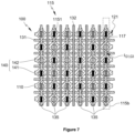
- THE figures 7 , 8 and 9 show a second embodiment of the quantum device 100.
- the second embodiment differs from the first embodiment, illustrated in figures 1 to 6 , in that the charge detectors 140 are not formed in the second grids 132 but in third grids 135 intended to control the chemical potential of the quantum dots 1151.
- the third grids 135 are therefore charge accumulation grids.
- the second grids 132 are then covered, on their sides and their upper face, with a layer 133' of insulating material forming a spacer 133' similar to the spacer 133.
- the spacer 133' then makes it possible to electrically insulate these second grids from the third grids 135.
- dielectric 121 is layer 120 of dielectric.
- the third grids are conductive strips formed from a conductive material similar to that forming the first and second grids.
- these third grids 135 are distinct from the second grids 132 and are all oriented in a direction Y' different from the first direction X of the first grids 131.
- the third grids and extend directly above the quantum boxes 1151.
- FIG. 7 shows a first variant embodiment of the second embodiment.
- the third grids are oriented at 90° relative to the first grids 131.
- each third grid 135 is arranged between two adjacent second grids, directly above the quantum dots arranged on the same column 115b of the matrix 115 of quantum dots.
- the third grids 135 extend directly over the dielectric 121 and intersect the first grids 131 (cf. Figure 7 ) in a nested configuration similar to the nested configuration described previously (in relation to the second grids132).
- the crossing zones between the first grids and the third grids are noted with the reference I G1,G3 on the figures 7 And 8 .
- FIG 8 shows a second variant embodiment of the second embodiment.
- the third grids are oriented at 45° relative to the first and second grids 131, 132.
- Each third grid 135 extends directly above the quantum boxes arranged on the same diagonal 115c of the matrix 115 of quantum boxes.
- the third grids 135 extend directly over the dielectric 121 and intersect the first and second grids in the same nested configuration as previously described.
- the crossing areas between the first grids and the third grids I G1,G3 correspond to the crossing areas between the first and second grids I G1,G2 .
- FIG. 9 shows, in schematic form, a sectional view of a third grid of the device shown in figure 8 .
- each third grid 135 extends directly over the dielectric 121 between two adjacent first grids 131 (or, in other words, in the inter-first grid spaces), and passes over, or overlaps, the first grids 131 coated with the spacer layer 133 at the level of the crossing zones I G1, G3 .
- the height of the third grids 135 is greater than that of the second grids 132.
- this height of the third grids is greater by 20 nm to 50 nm than that of the second grids 132.
- This nested configuration makes it possible to define a two-stage structure (a continuous conductive upper stage 137 and a lower stage formed of a plurality of lower conductive regions 1361) analogous to the structure of the second grids illustrated in Figure 6 .
- This nested configuration thus makes it possible to form in each third grid 135, or in a third grid 135 out of two, the internal structure described previously in relation to the first embodiment.
- each third grid presents the internal structure of the first type, illustrated in Figure 2 .
- one lower conductive region 1361 out of two forms a conductive island 141.
- the upper conductive region 137 forms the charge reservoir 142 common to all the islands formed in the third grid 135, and barrier patterns 1442 coated with the upper conductive region 137 form the gate terminals 144 (cf. Figure 9 ).
- This configuration makes it possible to position each conductive island 141 directly above a quantum dot (unlike the first embodiment, where the islands 141 are directly above the tunnel barriers).
- This arrangement allows a more localized measurement of the charge state of the quantum dot 1151 than when the charge detector 140 is directly above a tunnel barrier 1152b. Indeed, a charge detector 140 arranged directly above a quantum dot is more sensitive to the latter because it is closer than a charge detector arranged directly above a tunnel barrier. It is, however, less sensitive to neighboring quantum dots.
- the islands 141 are here arranged in a staggered pattern relative to each other.
- the third grids 135 may alternatively have the structure of the second type, illustrated in Figure 4 In this case, in the third grids 135, each lower conductive region 1361 forms a conductive island 141. A charge detector 140 is then arranged directly above each quantum box 1151.
- each third grid presents the internal structure of the second type, illustrated in Figure 6 .
- each lower conductive region 1361 forms a conductive island 141.
- the upper conductive region 137 forms the charge reservoir common to all the islands formed in the third grid, and barrier patterns coated with the upper conductive region form the drains 142.
- This configuration makes it possible to position a conductive island directly above each quantum box.
- the third grids can alternatively present the structure of the first type, illustrated in Figure 2 .
- the third grids 135 one lower conductive region 1361 out of two forms a conductive island 141.
- a charge detector 140 is then shared between two quantum boxes 1151.
- the quantum device 100 comprises two sets of control gates of the quantum dots 1151: the first set comprises the first gates 131; the second set comprises gates which extend directly over the dielectric 121 and intersect the first gates 132.
- the second set comprises, at least, the second gates 132.
- each charge detector 140 is formed by a region of one of the grids of the second set, said region being between two adjacent first grids 131 and arranged directly on the dielectric 121.
- the charge detector 140 may comprise only one charge reservoir 142, i.e., it may comprise only one source or one drain.
- connection of the island 141 of each load detector 140, or of a part thereof, to the related load reservoir 142 can be carried out only on one side of the island 141.
- the connection of the island 141 of the charge detector(s) 140 considered (and therefore of each related SET) with the upper stage 137 (forming the common charge reservoir 142) is made only on one of the sides of this island 141, indicated by the double arrow D in this figure.
- FIG. 10 shows a schematic representation of a block diagram of a process 800 for manufacturing the quantum device 100 illustrated in Figure 1 And 2 .
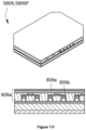
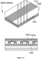
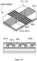
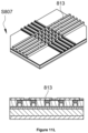
- FIGS. 11A to 11L are schematic representations in perspective and in sectional view illustrating certain steps or sub-steps of the manufacturing method 800.
- the manufacturing method 800 begins with a first step S801 of providing the SOI substrate 10 comprising on one of its faces the semiconductor layer 110. This first step S801 is illustrated in the Figure 11A .
- This step S801 is followed by a step S802 (cf. Figure 10 ) of definition of the arrangement of the quantum dot matrix 115 and the tunnel barriers 1152 in the semiconductor layer 110.
- this step S802 consists of determining the regions of the semiconductor layer 110 in which the quantum dots 1151 will be formed, as well as the regions in which the tunnel barriers 1152a, 1152b will be formed.
- This step S802 can be followed by a step of etching the semiconductor layer 110 to obtain the holes 117.
- the method 800 continues with a step S803 (cf. Figure 10 ) of depositing, on the entire upper face of the semiconductor layer 110, a first dielectric layer 121 with the material of the dielectric layer 120 of the dielectric 121
- This third step S803 is followed by a fourth step S804 aimed at jointly forming the first grids 131, and the tunnel layer 1441.
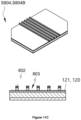
- this step S804 comprises the successive sub-steps S804A and S804B. These sub-steps are also illustrated in Figure 11B And 11C .
- sub-step S804A is a sub-step of forming a first stack 801 over the entire surface of the spacer 120, by:
- Sub-step S804B is a sub-step of three-dimensional structuring of the first stack 801 to form first strips 802 parallel to each other, arranged on the dielectric layer 120 opposite the first tunnel barriers 1152a defined previously.
- the structuring sub-step S804B is carried out by defining an etching mask in the first hard mask layer 8013, then by successive etchings, through the etching mask, of the second layer dielectric 8012 and the first conductive layer 8011, with a stop on the dielectric layer 120.
- the device obtained at the end of this sub-step S804B is represented on the Figure 11C .
- the bands 802 obtained are separated by free spaces 803 of the dielectric layer 120.
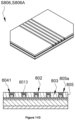
- Step S804 is followed by a fifth step S805 consisting of carrying out a conformal deposition of an encapsulation layer 8041 so as to cover the external limits of the first strips 802 and the free spaces 803.
- the encapsulation layer 8041 is produced with the material of the spacer 133. This deposition can be followed by a planarization of the encapsulation layer 8041 on the upper faces of the first strips 801.
- the insulating recesses 133 R of the second grids 132 are prepared.
- the method 800 continues with a sixth step S806, the aim of which is to jointly form the second grids 132 and the islands 141 in these second grids 132.
- step S806 preferably comprises the successive sub-steps S806A, S806B, S806C, S806D, S806E, S806F, S806G and S806H illustrated respectively in the figures 11D , 11th , 11F , 11G , 11 a.m. , 11I , 11J , And 11K .
- sub-step S806A consists of forming lower conductive strips 805 by filling the inter-first strip spaces 803 with the conductive material intended to form the second grids 132.
- the filling is carried out up to the height of the encapsulation layer 8041 arranged on the upper face of the first strips 802. This filling is advantageously followed by planarization of the deposited conductive layer to leave a flat upper surface 805a flush with the first strips 802.
- sub-step S806B consists of depositing, on the entire upper surface 805a formed at the end of step S806A, a stack 806 of barrier layers comprising: a lower barrier layer 8061 formed with the material of the tunnel layer 1441 and an upper barrier layer 8062 formed with the material of the barrier patterns 1442.
- Substep S806C which extends substep S806B consists of structuring in three dimensions the stack of dielectric layers 806 to form barrier strips 807.
- these barrier strips 807 are preferably parallel to each other and oriented at 45° relative to the first strips 801. Furthermore, in a direction X 1 perpendicular to the first strips 802. Furthermore, each barrier strip 807 covers a lower conductive strip 803 as well as the two adjacent first strips 801.
- the orientation of the barrier strips 807 makes it possible to achieve the desired periodicity of the charge detectors 140 in the quantum device 100.
- the 45° orientation makes it possible to achieve the periodicity of one island 141 formed in one lower conductive region 1361 out of two (i.e. one charge detector 140 for two quantum dots 1151).
- barrier strips 807 define the tunnel layer 1441 and make it possible to define the islands 141.
- the following sub-step S806D consists of carrying out an anisotropic etching of the upper barrier layer 8062 from the barrier strips 807, and with stopping on the lower barrier layer 8061.
- the final structure is illustrated in Figure 11G .
- the upper barrier layer 8062 forms an upper dielectric strip 807a whose lateral dimensions (along the X direction) are smaller than the dimension of the lower conductive strip 805c, and which is positioned in a central zone 8051 of this lower conductive strip 805c.
- the fourth dielectric layer 8061 forms a lower barrier strip 707b.
- Substep S806E illustrated in figure 11H consists of forming an upper conductive layer 808 by depositing the conductive material intended to form the second gates 132 on all of the lower and upper dielectric strips 807a, 807b and up to the level of these upper dielectric strips 807a.
- This sub-step S806E may further comprise an operation of planarizing the upper conductive layer 808.
- Sub-steps S806F, S806G and S806H aim to structure in three dimensions the stack 808a formed by the lower conductive strips 805 and the upper conductive layer 808 to form second conductive strips 809 parallel to each other and oriented perpendicular to the first strips 802, extending over the dielectric layer 120 and crossing the first strips by forming insulating bridges over these first strips 802.
- Substep S806F, illustrated in Figure 11I consists of forming one or more layers 809a, 809b intended to form a hard mask 809 over the entire planarized surface.
- Substep S806G illustrated in Figure 11J , consists of defining an etching mask in the hard mask layer 809, so as to define second strips 810 parallel to each other and oriented perpendicularly relative to the first strips 802, extending opposite the second tunnel barriers 1152b (not shown in the Figure 11J ), and each coating a plurality of portions of the barrier layers 807a, 807b.
- Sub-step S806H consists of carrying out selective etching through the hard mask 809, the structured dielectric strips 807a and 807b, the upper conductive strip 808 and the lower conductive strips 805, with a stop on the dielectric layer 120.
- the second strips 810 are formed. These second strips 810 correspond to the second grids with the charge detectors 140 formed within them.
- the manufacturing method can further continue with a step S807 consisting of removing the hard mask 809 remaining on the upper face of the second strips 810, then carrying out siliciding, for example by depositing a layer 813 of SiN on the second strips 810.
- Figure 11L illustrates the quantum device 100 obtained at the end of this step S807.
- the manufacturing method which has just been described makes it possible to manufacture the quantum device 100 according to the first embodiment (cf. Figure 1 ).
- Substep S806D is deleted.
- This way of carrying out the structuring of the dielectric strips is advantageous in that it reduces the number of steps to be carried out.
Landscapes
- Engineering & Computer Science (AREA)
- Physics & Mathematics (AREA)
- Theoretical Computer Science (AREA)
- General Physics & Mathematics (AREA)
- Mathematical Physics (AREA)
- Nanotechnology (AREA)
- Chemical & Material Sciences (AREA)
- Mathematical Optimization (AREA)
- Condensed Matter Physics & Semiconductors (AREA)
- Mathematical Analysis (AREA)
- Data Mining & Analysis (AREA)
- Pure & Applied Mathematics (AREA)
- Computing Systems (AREA)
- General Engineering & Computer Science (AREA)
- Evolutionary Computation (AREA)
- Software Systems (AREA)
- Computational Mathematics (AREA)
- Artificial Intelligence (AREA)
- Manufacturing & Machinery (AREA)
- Crystallography & Structural Chemistry (AREA)
- Light Receiving Elements (AREA)
- Investigating Or Analyzing Materials By The Use Of Electric Means (AREA)
- Solid State Image Pick-Up Elements (AREA)
Applications Claiming Priority (1)
| Application Number | Priority Date | Filing Date | Title |
|---|---|---|---|
| FR2312792A FR3155634A1 (fr) | 2023-11-21 | 2023-11-21 | Dispositif quantique et procédé de fabrication associé |
Publications (1)
| Publication Number | Publication Date |
|---|---|
| EP4561295A1 true EP4561295A1 (de) | 2025-05-28 |
Family
ID=90571763
Family Applications (1)
| Application Number | Title | Priority Date | Filing Date |
|---|---|---|---|
| EP24214630.6A Pending EP4561295A1 (de) | 2023-11-21 | 2024-11-21 | Zweidimenionale quantenvorrichtungsmatrix mit integrierten ladungsdetektoren und verfahren zur herstellung |
Country Status (3)
| Country | Link |
|---|---|
| US (1) | US20250169379A1 (de) |
| EP (1) | EP4561295A1 (de) |
| FR (1) | FR3155634A1 (de) |
Families Citing this family (1)
| Publication number | Priority date | Publication date | Assignee | Title |
|---|---|---|---|---|
| FR3143798B1 (fr) * | 2022-12-20 | 2025-12-12 | Commissariat Energie Atomique | Dispositif quantique destiné à former une matrice de boites quantiques et procédé de fabrication associé |
Citations (5)
| Publication number | Priority date | Publication date | Assignee | Title |
|---|---|---|---|---|
| EP2075745A1 (de) * | 2007-12-28 | 2009-07-01 | Hitachi Ltd. | Quanteninformationsverarbeitungsvorrichtung |
| FR3066297A1 (fr) | 2017-05-11 | 2018-11-16 | Commissariat A L'energie Atomique Et Aux Energies Alternatives | Dispositif quantique a qubits de spin |
| US20210296556A1 (en) * | 2020-03-22 | 2021-09-23 | Fu-Chang Hsu | Quantum bit array |
| WO2023277687A1 (en) * | 2021-06-29 | 2023-01-05 | Technische Universiteit Delft | Quantum dot structures comprising an integrated single electron tunneling readout and single electron tunneling quantum dot readout structures |
| EP4160694A1 (de) * | 2021-10-01 | 2023-04-05 | Commissariat à l'énergie atomique et aux énergies alternatives | Verfahren zur herstellung einer quantenelektronischen schaltung |
Family Cites Families (1)
| Publication number | Priority date | Publication date | Assignee | Title |
|---|---|---|---|---|
| US8829492B2 (en) * | 2010-11-05 | 2014-09-09 | Chungbuk National University Industry-Academic Cooperation Foundation | Multiple quantum dot device and a production method for the device |
-
2023
- 2023-11-21 FR FR2312792A patent/FR3155634A1/fr active Pending
-
2024
- 2024-11-21 US US18/954,945 patent/US20250169379A1/en active Pending
- 2024-11-21 EP EP24214630.6A patent/EP4561295A1/de active Pending
Patent Citations (6)
| Publication number | Priority date | Publication date | Assignee | Title |
|---|---|---|---|---|
| EP2075745A1 (de) * | 2007-12-28 | 2009-07-01 | Hitachi Ltd. | Quanteninformationsverarbeitungsvorrichtung |
| FR3066297A1 (fr) | 2017-05-11 | 2018-11-16 | Commissariat A L'energie Atomique Et Aux Energies Alternatives | Dispositif quantique a qubits de spin |
| EP3401848B1 (de) * | 2017-05-11 | 2021-07-28 | Commissariat À L'Énergie Atomique Et Aux Énergies Alternatives | Quantenvorrichtung mit spin-qubits |
| US20210296556A1 (en) * | 2020-03-22 | 2021-09-23 | Fu-Chang Hsu | Quantum bit array |
| WO2023277687A1 (en) * | 2021-06-29 | 2023-01-05 | Technische Universiteit Delft | Quantum dot structures comprising an integrated single electron tunneling readout and single electron tunneling quantum dot readout structures |
| EP4160694A1 (de) * | 2021-10-01 | 2023-04-05 | Commissariat à l'énergie atomique et aux énergies alternatives | Verfahren zur herstellung einer quantenelektronischen schaltung |
Non-Patent Citations (1)
| Title |
|---|
| FLORIS A. ZWANENBURG ET AL: "Silicon quantum electronics", REVIEWS OF MODERN PHYSICS, vol. 85, no. 3, 1 July 2013 (2013-07-01), pages 961 - 1019, XP055718734, ISSN: 0034-6861, DOI: 10.1103/RevModPhys.85.961 * |
Also Published As
| Publication number | Publication date |
|---|---|
| US20250169379A1 (en) | 2025-05-22 |
| FR3155634A1 (fr) | 2025-05-23 |
Similar Documents
| Publication | Publication Date | Title |
|---|---|---|
| EP3401848B1 (de) | Quantenvorrichtung mit spin-qubits | |
| EP3701567B1 (de) | Verfahren zur herstellung eines elektronischen bauteils mit doppelquantenpunkten | |
| FR3086456A1 (fr) | Procede de realisation de transistors superposes | |
| FR2713016A1 (fr) | Dispositif semiconducteur à haute intégration et procédé pour la fabrication de celui-ci. | |
| FR2919112A1 (fr) | Circuit integre comprenant un transistor et un condensateur et procede de fabrication | |
| EP4092750A1 (de) | 1t1r-speicher mit 3d-struktur | |
| EP4561295A1 (de) | Zweidimenionale quantenvorrichtungsmatrix mit integrierten ladungsdetektoren und verfahren zur herstellung | |
| FR3033665A1 (fr) | Transistor a electron unique et son procede de realisation | |
| EP4060748B1 (de) | Vorrichtung mit zwei übereinanderliegenden ebenen von elektrostatischen steuergittern | |
| FR2985593A1 (fr) | Procede de fabrication d'une cellule memoire non volatile a double grille | |
| EP3843158A1 (de) | Vorrichtung umfassend transistoren mit rundum-gate und herstellungsverfahren einer solchen vorrichtung | |
| FR3118961A1 (fr) | Dispositif comprenant des grilles de commande électrostatique reparties sur deux faces opposées d’une portion de semi-conducteur | |
| FR2899381A1 (fr) | Procede de realisation d'un transistor a effet de champ a grilles auto-alignees | |
| EP4561293A1 (de) | Quantenvorrichtungen, bestehend aus einer matrix von quantenboxen und integrierten ladungsdetektoren, sowie verfahren zur herstellung dieser vorrichtungen | |
| EP4391068A1 (de) | Quantenvorrichtung zur formung einer quantenpunktmatrix und herstellungsverfahren dafür | |
| EP4369884A1 (de) | Dreidimensionale struktur von nor-speichern | |
| EP3843143B1 (de) | 3d-speicher und dessen herstellungsverfahren | |
| FR2830686A1 (fr) | Transistor a un electron et a canal vertical, et procedes de realisation d'un tel transistor | |
| EP1677347B1 (de) | Magnetischer Speicher | |
| FR3126063A1 (fr) | Dispositif pour le stockage, le contrôle et la manipulation de l’information quantique (qubits) sur semi-conducteur | |
| EP4086822B1 (de) | Vorrichtung mit elementen zur kompensation der lokalen variabilität des elektrostatischen potenzials | |
| EP4572593B1 (de) | Verfahren zur herstellung einer speichervorrichtung und eine speichervorrichtung | |
| EP4435867A1 (de) | Quantenelektronische schaltung und herstellungsverfahren dafür | |
| EP4561294A1 (de) | Zweidimensionale quantenmatrixvorrichtung und herstellungsverfahren dafür | |
| EP4633324A1 (de) | Quantenpunkt-matrix-vorrichtung mit kopplungsbereiche, mit gates auf gegenüberliegenden seiten der quantenpunkt-matrix |
Legal Events
| Date | Code | Title | Description |
|---|---|---|---|
| PUAI | Public reference made under article 153(3) epc to a published international application that has entered the european phase |
Free format text: ORIGINAL CODE: 0009012 |
|
| STAA | Information on the status of an ep patent application or granted ep patent |
Free format text: STATUS: REQUEST FOR EXAMINATION WAS MADE |
|
| 17P | Request for examination filed |
Effective date: 20241121 |
|
| AK | Designated contracting states |
Kind code of ref document: A1 Designated state(s): AL AT BE BG CH CY CZ DE DK EE ES FI FR GB GR HR HU IE IS IT LI LT LU LV MC ME MK MT NL NO PL PT RO RS SE SI SK SM TR |