EP3401932A1 - Circuit électrique pour compensation d'une résistance électrique - Google Patents
Circuit électrique pour compensation d'une résistance électrique Download PDFInfo
- Publication number
- EP3401932A1 EP3401932A1 EP17170814.2A EP17170814A EP3401932A1 EP 3401932 A1 EP3401932 A1 EP 3401932A1 EP 17170814 A EP17170814 A EP 17170814A EP 3401932 A1 EP3401932 A1 EP 3401932A1
- Authority
- EP
- European Patent Office
- Prior art keywords
- section
- trimming
- current path
- resistor
- current
- Prior art date
- Legal status (The legal status is an assumption and is not a legal conclusion. Google has not performed a legal analysis and makes no representation as to the accuracy of the status listed.)
- Granted
Links
Images

Classifications
-
- H—ELECTRICITY
- H01—ELECTRIC ELEMENTS
- H01C—RESISTORS
- H01C10/00—Adjustable resistors
- H01C10/06—Adjustable resistors adjustable by short-circuiting different amounts of the resistive element
-
- H—ELECTRICITY
- H01—ELECTRIC ELEMENTS
- H01C—RESISTORS
- H01C10/00—Adjustable resistors
- H01C10/14—Adjustable resistors adjustable by auxiliary driving means
-
- H—ELECTRICITY
- H01—ELECTRIC ELEMENTS
- H01C—RESISTORS
- H01C17/00—Apparatus or processes specially adapted for manufacturing resistors
- H01C17/22—Apparatus or processes specially adapted for manufacturing resistors adapted for trimming
Definitions
- the disclosure relates to an electric circuit for trimming a resistance of a resistor in a current path.
- the disclosure further relates to a method for trimming a resistance of the resistor.
- Integrated resistors usually undergo a large spread versus process. Starting from a typical value, a variation of a resistance of a resistor as large as +/- 20% can usually be observed in different production lots.
- One of the most typical applications which is affected by this problem is a voltage-to-current converter by means of which a precise reference current is obtained on a chip by loading a bandgap voltage with a resistor. Since the bandgap voltage is usually trimmed as well, the large resistor spread creates a 20% inaccuracy of the generated current.
- the resistance of the resistor should be tuned from 84% to 116% of its nominal value in 6 bits.
- the two extreme values of the resistance range correspond to the trimming options to be selected in cases where the process provides a resistance of the resistor that is 16% bigger than the nominal resistance and 16% smaller than the nominal resistance, respectively.
- the resistance of a resistor does not need to be trimmed from a value of 0 Ohm to the highest possible value.
- the minimum value of the resistance is largely greater than 0 Ohm.
- An electric circuit for trimming a resistance of a resistor which does not consume a large area and allows to trim the resistance of the resistor with high accuracy is specified in claim 1.
- the circuit for trimming the resistance of the resistor comprises a current path including a first section and at least a second section, wherein the first and the at least one second section are connected in series in the current path.
- the first section of the current path includes the resistor to be trimmed.
- the electric circuit may comprise several of the at least one second section in the current path.
- the at least one second section of the current path includes a first current branch and a second current branch being connected in parallel.
- the first current branch of the at least one fifth section of the current path includes a first and a second trimming resistor being connected in parallel.
- the second current branch of the at least one second section of the current path includes a third trimming resistor and a fourth trimming resistor being connected in parallel.
- the second current branch of the at least one second section of the current path includes at least one fifth trimming resistor being connected in series to the parallel connection of the third and the fourth trimming resistor.
- the second current branch of the at least one second section of the current path includes a controllable switch. The controllable switch of the at least one second section of the current path is connected in series to the parallel connection of the third and the fourth trimming resistor.
- the controllable switch of the at least one second section of the current path is configured to electrically connect the second current branch of the at least one second section of the current path, and thus the parallel connection of the third and the fourth trimming resistor, in parallel to the first current branch of the at least one second section of the current path, when the controllable switch of the at least one second section of the current path is operated in the closed state.
- the controllable switch of the at least one second section of the current path is further configured to isolate the second current branch of the at least one second section of the current path, and thus the parallel connection of the third and the fourth trimming resistor, from the first current branch of the at least one second section of the current path, when the controllable switch of the at least one second section of the current path is operated in the open state.
- the current path may further comprise a third section being connected in series to the first section of the current path.
- the third section of the current path may comprise a sixth trimming resistor and a controllable switch.
- the controllable switch of the third section of the current path is configured to electrically connect the sixth trimming resistor in series to the first section of the current path and further in series to the at least one second section of the current path, when the controllable switch is turned in an open state. In the closed state, the controllable switch of the third section of the current path is configured to bypass the sixth trimming resistor so that the first section of the current path is connected to the at least one second section of the current path via the closed controllable switch of the third section of the current path.
- the current path may comprise a fourth section being connected in series to the third section and the at least one second section of the current path.
- the fourth section of the current path may comprise a seventh trimming resistor and an eighth trimming resistor being connected in parallel.
- the fourth section of the current path may comprise a controllable switch that is configured to connect the parallel connection of the seventh and the eighth trimming resistor in series between the second section and the third section of the current path, when the controllable switch is operated in an open state.
- the controllable switch of the fourth section of the current path is further configured to bypass the parallel connection of the seventh and the eighth trimming resistor so that the third section of the current path is electrically connected to the at least one second section of the current path via the controllable switch of the fourth section of the current path, when the controllable switch of the fourth section of the current path is operated in the closed state.
- the current path includes a fifth section comprising a first current branch and a second current branch.
- the first current branch of the fifth section of the current path includes at least a ninth trimming resistor.
- the second current branch of the fifth section of the current path includes a series connection of a controllable switch and at least a tenth and an eleventh and a twelfth trimming resistor.
- the controllable switch of the second current branch of the fifth section of the current path is configured to electrically connect the at least one tenth and eleventh and twelfth trimming resistor of the second current branch of the fifth section of the current path in parallel to the at least one ninth trimming resistor of the first current branch of the fifth section of the current path, when the controllable switch of the second current branch of the fifth section of the current path is operated in a closed state.
- a method for trimming a resistance of a resistor is specified in claim 12.
- the resistance of the (fixed) resistor is trimmed by closing or opening at least one of the controllable switches of the at least one second, the third, the fourth and the fifth section of the current path in dependence on the sections provided in the current path and thus in dependence on the available trimming steps/sections.
- FIG. 1 shows a first embodiment of an electric circuit 1 to trim a resistance of a fixed resistor Rfix.
- the electric circuit 1 comprises a current path 10 being connected between a supply potential VDD and a reference potential VSS.
- the current path comprises a section 11 comprising the (fixed) resistor Rfix.
- the electric circuit 1 may comprise a plurality of sections 12, 13, 14, ..., 1m of the current path 10 in dependence on the trimming accuracy or trimming step size of the resistance of the resistor Rfix.
- Each of the sections may comprise a respective controllable switch S12, S13, S14, ..., S1m and a respective trimming resistor R12, R13, R14, ..., R1m.
- Figure 1 shows the trimming resistors having a resistance R.
- the sections 12, 13, 14, ..., 1m are connected in series in the current path 10 subsequent to the section 11 of the current path that includes the resistor Rfix.
- Each of the respective controllable switches S12, S13, S14, ..., S1m of the sections 12, 13, 14, ..., 1m of the current path 10 may be configured to connect the respective trimming resistor R12, R13, R14, ..., R1m of the sections of the current path 10 in series to a previous and a subsequent section of the current path 10, when the respective controllable switch is operated in the open state.
- each of the controllable switches of the current section 12, 13, 14, ..., 1m is configured to bypass the respective trimming resistor of the respective section of the current path.
- the electric circuit shown in Figure 1 enables to trim the resistance of the (fixed) resistor Rfix by controlling the respective controllable switches S12, S13, S14, ..., S1m of the sections 12, 13, 14, ..., 1m of the current path 10 in the closed or open state. It is clear that, still referring for the sake of simplicity, but not exclusively, to the range 84% to 116% of the resistance of the resistor Rfix with 6 trimming bits, the resistor Rfix is trimmed by using a respective trimming resistor in each of the sections 12, 13, 14, ..., 1m of the current path which is 0.5% of the nominal resistance of the fixed resistor Rfix and put 232 of theses unity elements/trimming resistors in series.
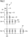
- a unity trimming resistor should be shaped with an L/W ratio (Length/Width ratio) that is quite large so that parasitic contributions of contacts and border effects are negligible. This becomes a serious problem if the total resistance of the resistor to be trimmed is not very large. Under the recommendation that a unity resistor should have at least five (or even ten) squares, this means that if the total resistance of the resistor Rfix is below 1,160 (or 2,320) squares, the less significant bits should be obtained with more trimming resistors in parallel in each of the sections of the current path, as shown in Figure 2 .
- Figure 2 shows a second embodiment of an electric circuit for trimming a resistance of a (fixed) resistor Rfix.
- Figure 2 illustrates how the structure of Figure 1 changes in the case that the LSB trimming resistor should be obtained as a parallel connection of bigger elements to comply with the minimum L/W rule.
- the embodiment of the electric circuit 2 shown in Figure 2 comprises a current path 20 comprising a plurality of sections 21, 22, 23, 24, ..., 2m.
- the current path 20 with the sections 21 to 20m is connected between a supply potential VDD and a reference potential VSS.
- the section 21 of the current path 20 comprises the (fixed) resistor Rfix to be trimmed.
- the subsequent section 22 that is connected in series to the section 21 of the current path 20 comprises a trimming resistor R22 that may be bypassed by a controllable switch S22.
- Each of the subsequent sections 23, 24, ..., 2m of the current path 20 comprises an increasing number of trimming resistors R22, R23, R24, ..., R2m per section, wherein the trimming resistors are connected in parallel in each of the sections 23, 24, ..., 2m.
- each of the sections 23, 24, ..., 2m of the current path 20 comprises a respective controllable switch S22, S23, S24, ..., S2m to bypass the parallel connection of the trimming resistors of the respective section of the current path 20.
- the respective controllable switch of each of the subsequent sections 22, 23, 24, ..., 2m of the current path 20 may be switched in a closed or open state.
- the LSB generation in the last section 2m of the current path 20 comprises 2 m-2 trimming resistors.
- a polyh resistor (1,200 Ohm per square) is considered to realistically generate 16 ⁇ A under a bandgap voltage. This requires a 75 kilo Ohm resistor, i.e. a little more than 60 squares.
- the second least significant digit would be made by connecting 16 trimming resistors in parallel, then 8 trimming resistors for the third least significant digit, then 4 trimming resistors, 2 trimming resistors and one trimming resistor to complete the trimming section, as shown in Figure 2 .
- this allows the possibility to tune the resistance of the resistor Rfix in a range as large as 24 kilo Ohm, i.e. +/- 16% from the nominal resistance value.
- the resistor Rfix will be trimmed from 63 kilo Ohm to 87 kilo Ohm in steps of 375 Ohm, and a total of 63 unit 10 square resistors will be used for trimming.
- the remaining untrimmed contribution, amounting to 63 kilo Ohm, is easily arranged with five series units plus four units in parallel. As a result, the trimming part of the electric trimming circuit would be seven times larger than the untrimmed portion.
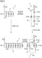
- Figure 3 shows two alternative embodiments of sections of a trimming circuit to generate the same variation of a resistance for a fixed resistor.
- Figure 3 shows, on the left side, the portion 24 of the electric circuit 2 for trimming the resistance of the resistor Rfix.
- the portion 24 comprises the four trimming resistors R24 having a resistance R.
- the trimming resistors may be bypassed by closing the controllable switch S24.
- the section 24 of the electric circuit 2 allows to vary the resistance of the resistor Rfix from 0 Ohm to R/4 Ohm depending on the switching status of the controllable switch S24.
- Figure 3 shows, on the right side, a section 120 of another embodiment of an electric circuit 3 for trimming the resistance of the resistor Rfix.
- the section 120 of the electric circuit 3 comprises a current branch 121 and a current branch 122 that may be connected in parallel by means of a controllable switch S3.
- the current branch 121 of the section 120 of the trimming circuit includes a single trimming resistor R120a having a resistance R.
- the current branch 122 includes a series connection of three trimming resistors R120b, R120c and R120d having a resistance R.
- the trimming resistors R120b, R120c and R120d can be electrically connected in parallel to the trimming resistor R120a, if the controllable switch S3 is turned in a conductive/closed state. In this way, the total resistance varies from 3 ⁇ 4 R to R.
- both embodiments fit the requirement to vary a resistance of a resistor Rfix by the same resistance step, where a resistance of 0 Ohm is not an option.
- the minimum resistance must be at least equal to 3 ⁇ 4 R.
- the same tuning capability is ensured. The difference in the total resistance can be easily corrected by making the untrimmed part consequently smaller, if the architecture of the trimming circuit 3 shown in the right side of Figure 3 is used.
- Figure 3 shows, in the bottom portion, on the left hand side a section 25 of the approach of the trimming circuit 2 and on the right hand side a section 150 of the approach of the trimming circuit 3 to arrange a smaller step of a resistance variation, i.e. a resistance variation of R/8.
- the number of trimming resistors R25 being connected in parallel in the section 25 of the trimming circuit 2 is doubled in comparison to the number of trimming resistors R24 of the section 24 to realize the resistance variation of R/8.
- the section 25 of the trimming circuit 2 comprises 8 trimming resistors.
- the 8 parallel connected trimming resistors R25 may be bypassed by a controllable switch S25.
- any single trimming resistor in the current branches 121 and 122 is replaced by two trimming resistors in parallel, while the series of two trimming resistors in the current branch 122 is replaced by only one trimming resistor.
- the trimming resistor R120a is replaced by the two trimming resistors R150a and R150b connected in parallel in the current branch 151 of the section 150 of the trimming circuit 3.
- the series connection of the two trimming resistors R120c and R120d of the section 120 of the trimming circuit 3 is replaced by a single trimming resistor R150e.
- the single trimming resistor R120b is replaced by the two trimming resistors R150c and R150d being connected in parallel in the current branch 152 of the section 150 of the trimming circuit 3.
- the controllable switch S3 of the section 120 of the trimming circuit 3 arranged in the current branch 122 remains unchanged and corresponds to the controllable switch S4 included in the current branch 152 of the section 150 of the trimming circuit 3.
- the section 25 of the trimming circuit 2 and the section 150 of the trimming circuit 3 are compared, it can be realized that the number of trimming resistors in the section 150 of the trimming circuit 3 is only increased by one, whereas the number of trimming resistors in the section 25 is doubled in comparison to the section 24 of the trimming circuit 2.
- the architecture of the trimming circuit 3 using the section 150 only uses five trimming resistors instead of eight trimming resistors in the section 25 of the trimming circuit 2.
- the configuration of the trimming circuit 3 enables to save area on a supporting substrate, for example a printed circuit board, of the trimming circuit.
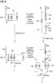
- Figure 4 generalizes the concept how the (N+1)th trimming section is obtained from the (N)th one for both approaches of the trimming circuits 2 and 3 shown in Figure 3 .
- Figure 4 illustrates the two alternative embodiments of respective sections of the trimming circuits 2 and 3 to generate the resistance variation with a step size of 1/2 N+1 starting from the 1/2 N step of resistance variation with M being a positive integer.
- Section 50 of the circuit approach 3 on the top right side of Figure 4 is another way to make a 1/2 N step of resistance change if compared to the structure 40 shown on the top left side of Figure 4 .
- both sections 40 and 50 use the same number of trimming resistors.
- the section 40 of the trimming circuit approach 2 shown on the left side of the top portion of Figure 4 uses 2 N parallel trimming resistors 30 which can be bypassed by a controllable switch S40.
- the section 50 of the other trimming circuit approach 3 shown on the right side of the top portion of Figure 4 uses one trimming resistor 53a in a current branch 51 and a series connection of 2 N -1 trimming resistors 53a, 53b, ..., 53n in a second current branch 52 that can be electrically connected in parallel to the current branch 51 by a controllable switch S50. If the switchable series of 2 N -1 similar trimming resistors 53b, 53c, ..., 53n is put in parallel to the single trimming resistor 53a, the generation of a R/2 N wide trimming step is obtained, changing the resistance from R to R ⁇ 1 ⁇ 1 / 2 N .
- the resistances in both current paths 51 and 52 are halved. That means that the single resistor 53a in the current branch 51 is replaced by a parallel connection of two trimming resistors 73a and 73b in the current branch 71. Furthermore, the series connection of the trimming resistors 53b, 53c, ..., 53n in the current branch 52 is replaced by a series connection of 2 N-1 -1 trimming resistors in the current branch 72 and a parallel connection of two trimming resistors 73c and 73d.
- the section 70 of the trimming circuit 3 comprises a controllable switch S70 that is configured to connect the current branches 71 and 72 electrically in parallel.
- the 1/2 N+1 step of resistance change is obtained with 3 + 2 N-1 trimming resistors, if the embodiment of the trimming circuit 3 is used.
- making the impedance halved using the approach of the trimming circuit 3 means to halve the number of trimming resistors connected in series in the current branch 72, not doubling them as shown for the configuration of the section 60 of the trimming circuit 2.
- the switchable path 52 including an odd number of trimming resistors the next LSB generation according to the scheme of the trimming circuit 3 requires 3 + 2 N-1 trimming resistors in total instead of 2 N+1 trimming resistors for the respective section of the trimming circuit 2. Large area savings follows, especially for large values of N.
- the table below shows the trimming step size (1/2 N+1 ) of the resistance change and the number of trimming resistors used in the last sections of the trimming circuits 2 and 3.
- N being an integer with N ⁇ 1
- the number of trimming resistors in the last section of the current path of the trimming circuit 2 according to the embodiment 2 results in 2 N+1
- number of trimming resistors in the last section of the current path of the trimming circuit 2 according to the embodiment 3 results in 3 + 2 N-1 .
- Trimming step size N Number of trimming resistors in last section of current path of embodiment 2 of trimming circuit Numbers of trimming resistors in last section of current path of embodiment 3 of trimming circuit 1/4 1 4 4 1/8 2 8 5 1/16 3 16 7 1/32 4 32 11 1/64 5 64 19
- Figures 5 and 6 respectively show an example for the trimming circuit 2 and 3 of the different approaches.
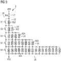
- Figure 5 shows an embodiment of an electric circuit 2 for trimming a resistance of a resistor Rfix using the approach illustrated on the left side of Figure 4 .
- Figure 6 shows an electric circuit 3 for trimming a resistance of a resistor Rfix using the approach shown on the right side of Figure 4 .
- FIG 5 shows an embodiment of a 5-bit trimming approach of an electric circuit for trimming a resistance of the resistor Rfix.
- the configuration of the electric circuit 2 is based on the approach illustrated in Figure 2 or in the left portions of Figures 3 and 4 .
- the electric circuit 2 comprises a current path 20 including a plurality of sections 21, 22, 23, 24, 25 and 26 being connected in series between a supply potential VDD and a reference potential VSS.
- the section 21 of the current path 20 comprises the (fixed) resistor Rfix of which its resistance is trimmed by the trimming sections 22, 23, 24, 25 and 26.
- the trimming section 22 comprises a single resistor R22 that can be bypassed by a controllable switch S1.
- the subsequent trimming section 23 comprises the two parallel connected resistors R23 that may be bypassed by the controllable switch S2.
- the trimming circuit 2 further comprises the trimming section 24 including the four parallel connected trimming resistors R24 that may be bypassed by a controllable switch S3.
- the subsequently arranged trimming section 25 comprises eight trimming resistors R25 that can be bypassed by the controllable switch S4.
- the last trimming section 26 comprises sixteen trimming resistors R26 that can be bypassed by the controllable switch S5.
- the controllable switches S1, ..., S5 may be controlled to be turned in a closed or open state by means of a controller circuit not shown in Figure 5 .
- the (fixed) resistor Rfix can be trimmed to different resistances.
- the embodiment of the electric trimming circuit 2 shown in Figure 5 to realize the 5-bit trimming approach includes 31 trimming resistors in the several trimming sections 22 to 26 having the same resistance R.
- Figure 5 illustrates that a trimming section is doubled with parallel resistors in the subsequent trimming section to generate the next lower LSB.
- Each trimming section can be bypassed by the corresponding controllable switch S1, ..., S5 to modulate the value of the (fixed) resistor Rfix.
- Figure 5 clearly shows that the area increase for the trimming circuit 2 is exponential with the number of bits. K bits require 2 K -1 trimming resistors.
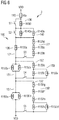
- FIG. 6 shows an embodiment of an electric circuit 3 for trimming a resistance of a (fixed) resistor Rfix.
- the circuit 3 comprises a current path 100 including a section 110 and a section 120.
- the section 110 and the section 120 are connected in series in the current path 10.
- the section 110 includes the fixed resistor Rfix to be trimmed.
- the section 120 of the current path 100 includes a current branch 121 and a current branch 122.
- the current branch 121 of the trimming section 120 of the current path 100 includes at least a trimming resistor R120a.
- the current branch 122 of the trimming section 120 of the current path 100 includes a series connection of a controllable switch S3 and at least a trimming resistor R120b, a trimming resistor R120c and a trimming resistor R120d.
- the current branch 122 comprises at least three trimming resistors.
- the controllable switch S3 of the current branch 122 of the trimming section 120 of the current path 100 is configured to connect the current path 122, i.e. the trimming resistors R120b, R120c and R120d in parallel to the current path 121, i.e. the trimming resistor R120a, when the controllable switch S3 is operated in the closed state.
- the current path 100 further comprises a trimming section 130 being connected in series to the section 110 of the current path 100.
- the trimming section 130 of the current path 100 includes a trimming resistor R130 and a controllable switch S1.
- the controllable switch S1 is configured to connect the trimming resistor R130 in series to the section 110 of the current path 100, i.e. to the (fixed) resistor Rfix, when the controllable switch S1 is turned in an open state.
- the controllable switch S1 is further configured to bypass the trimming resistor R130 so that the section 110 of the current path 100, i.e. the (fixed) resistor Rfix is connected to the trimming section 120 of the current path 100 by/via the controllable switch S1, when the controllable switch S1 of the trimming section 130 of the current path 100 is turned in the closed state.
- the current path 100 further comprises a trimming section 140 being connected in series between the trimming section 130 and the trimming section 120 of the current path 100.
- the trimming section 140 includes a trimming resistor R140a and a trimming resistor R140b being connected in parallel.
- the trimming section 140 further comprises a controllable switch S2 being configured to be operated in a closed and an open state.
- the controllable switch S2 of the trimming section 140 of the current path 100 is configured to connect the parallel connection of the trimming resistors R140a and R140b in series between the trimming section 120 and the trimming section 130 of the current path 100, when the controllable switch S2 is operated in the open state.
- the controllable switch S2 of the trimming section 140 is further configured to bypass the parallel connection of the trimming resistors R140a and R140b so that the trimming section 130 is connected to the trimming section 120 of the current path by/via the controllable switch S2, when the controllable switch S2 is operated in the closed state.
- the current path 100 includes at least one other trimming section being connected in series to the first, the second, the third and the fourth trimming section 110, 120, 130, 140 of the current path 100.
- the current path 100 comprises the trimming section 150 and the additional trimming section 150' that are both connected in series to the first, the second, the third and the fourth trimming section 110, 120, 130, 140 of the current path 100.
- the trimming section 150 of the current path 100 includes a current branch 151 and a current branch 152.
- the current branch 151 of the trimming section 150 includes a trimming resistor R150a and a trimming resistor 150b being connected in parallel.
- the current branch 152 includes a trimming resistor R150c and a trimming resistor R150d being connected in parallel.
- the current branch 152 of the trimming section 150 of the current path 100 further includes at least one trimming resistor R150e being connected in series to the parallel connection of the trimming resistors R150c and R150d.
- the current branch 152 of the trimming section 150 of the current path 100 further includes a controllable switch S4.
- the controllable switch S4 is connected in series to the parallel connection of the trimming resistors R150c and R150d.
- the controllable switch S4 of the trimming section 150 is configured to connect the current branch 152 in parallel to the current branch 151, when the controllable switch S4 of the trimming section 150 is operated in the closed state.
- the controllable switch S4 is further configured to isolate/separate the current branch 152 from the current branch 151, when the controllable switch S4 is operated in the open state.
- the current path 100 comprises the additional trimming section 150' being connected in series to the previous trimming sections 110, 120, 130, 140 and 150.
- the trimming section 150' includes a current branch 151' and a current branch 152' being connected in parallel.
- the current branch 151' comprises a trimming resistor R150'a and a trimming resistor R150'b being connected in parallel in the current branch 151'.
- the current branch 152' includes a trimming resistor R150'c and a trimming resistor R150'd being connected in parallel.
- the current branch 152' includes three trimming resistors R150'e, R150'f and R150'g being connected in series to the parallel connection of the trimming resistors R150'c and R150'd.
- the current branch 152' further comprises a controllable switch S5 that is connected in series to the parallel connection of the trimming resistors R150'c and R150'd.
- the controllable switch S5 of the current branch 152' is configured to connect the current branch 152' in parallel to the current branch 151', when the controllable switch S5 is operated in the closed state.
- the controllable switch S5 is further configured to isolate/separate the current branches 151' and 152' and thus the parallel connection of the trimming resistors R150'c and R150'd of the current branch 152' from the current branch 151', when the controllable switch S5 is operated in the open state.
- the at least one other trimming section comprises the trimming section 150 and the trimming section 150'.
- Each of the current branches 152 and 152' includes an odd number of trimming resistors R150e or R150'e, R150'f and R150'g being connected in series to the parallel connection of the trimming resistors R150c, R150d or R150'c, R150'd.
- Each of the trimming resistors in the trimming sections 130, ..., 150, 150' can have the same resistance R.
- each of the controllable switches S1 to S5 can be switched in the open or closed state.
- the approaches of the electric trimming circuits 2 and 3 are compared, it can be asserted that, as any bit adds an offset. This means that the untrimmed part of the resistance is smaller if the approach of the electric trimming circuit 3 is used. This saves additional area.
- the controllable switches of the sections of the electric trimming circuit 3 are always connected in series to several trimming resistors, unlike in the approach of the trimming circuit 2. In this way, the on-resistance of the controllable switches is less relevant in determining the trimming accuracy. This makes another remarkable saving of area.
- the switch size of the controllable switches in the trimming sections of the trimming circuit 3 is smaller in comparison to the switch size of the controllable switches in the trimming sections of the trimming circuit 2.
- INL integrated non-linearity
- DNL differential non-linearity
Landscapes
- Engineering & Computer Science (AREA)
- Microelectronics & Electronic Packaging (AREA)
- Manufacturing & Machinery (AREA)
- Apparatuses And Processes For Manufacturing Resistors (AREA)
- Semiconductor Integrated Circuits (AREA)
- Attenuators (AREA)
Priority Applications (1)
| Application Number | Priority Date | Filing Date | Title |
|---|---|---|---|
| EP17170814.2A EP3401932B1 (fr) | 2017-05-12 | 2017-05-12 | Circuit électrique pour compensation d'une résistance électrique |
Applications Claiming Priority (1)
| Application Number | Priority Date | Filing Date | Title |
|---|---|---|---|
| EP17170814.2A EP3401932B1 (fr) | 2017-05-12 | 2017-05-12 | Circuit électrique pour compensation d'une résistance électrique |
Publications (2)
| Publication Number | Publication Date |
|---|---|
| EP3401932A1 true EP3401932A1 (fr) | 2018-11-14 |
| EP3401932B1 EP3401932B1 (fr) | 2023-01-25 |
Family
ID=58873601
Family Applications (1)
| Application Number | Title | Priority Date | Filing Date |
|---|---|---|---|
| EP17170814.2A Active EP3401932B1 (fr) | 2017-05-12 | 2017-05-12 | Circuit électrique pour compensation d'une résistance électrique |
Country Status (1)
| Country | Link |
|---|---|
| EP (1) | EP3401932B1 (fr) |
Cited By (3)
| Publication number | Priority date | Publication date | Assignee | Title |
|---|---|---|---|---|
| US20220189668A1 (en) * | 2020-12-15 | 2022-06-16 | Ablic Inc. | Resistance device and current detection circuit including the resistance device |
| CN116632002A (zh) * | 2023-07-24 | 2023-08-22 | 江苏兴宙微电子有限公司 | 一种电阻修调电路、设计方法及其设计装置 |
| CN118783950A (zh) * | 2024-07-09 | 2024-10-15 | 上海璟派半导体有限公司 | 电阻修调电路、方法、集成电路及计算机可读存储介质 |
Families Citing this family (1)
| Publication number | Priority date | Publication date | Assignee | Title |
|---|---|---|---|---|
| US20250292849A1 (en) * | 2024-03-15 | 2025-09-18 | Everspin Technologies, Inc. | Reference resistor having variable resistance |
Citations (3)
| Publication number | Priority date | Publication date | Assignee | Title |
|---|---|---|---|---|
| US5243319A (en) * | 1991-10-30 | 1993-09-07 | Analog Devices, Inc. | Trimmable resistor network providing wide-range trims |
| US20060266646A1 (en) * | 2005-05-24 | 2006-11-30 | Hiroyuki Kimura | Trimming circuit and electronic circuit |
| US20080218248A1 (en) * | 2007-03-06 | 2008-09-11 | Kim Uladzimir | Circuit for Adjusting Reference Voltage Using Fuse Trimming |
-
2017
- 2017-05-12 EP EP17170814.2A patent/EP3401932B1/fr active Active
Patent Citations (3)
| Publication number | Priority date | Publication date | Assignee | Title |
|---|---|---|---|---|
| US5243319A (en) * | 1991-10-30 | 1993-09-07 | Analog Devices, Inc. | Trimmable resistor network providing wide-range trims |
| US20060266646A1 (en) * | 2005-05-24 | 2006-11-30 | Hiroyuki Kimura | Trimming circuit and electronic circuit |
| US20080218248A1 (en) * | 2007-03-06 | 2008-09-11 | Kim Uladzimir | Circuit for Adjusting Reference Voltage Using Fuse Trimming |
Cited By (4)
| Publication number | Priority date | Publication date | Assignee | Title |
|---|---|---|---|---|
| US20220189668A1 (en) * | 2020-12-15 | 2022-06-16 | Ablic Inc. | Resistance device and current detection circuit including the resistance device |
| US11948708B2 (en) * | 2020-12-15 | 2024-04-02 | Ablic Inc. | Resistance device and current detection circuit including the resistance device |
| CN116632002A (zh) * | 2023-07-24 | 2023-08-22 | 江苏兴宙微电子有限公司 | 一种电阻修调电路、设计方法及其设计装置 |
| CN118783950A (zh) * | 2024-07-09 | 2024-10-15 | 上海璟派半导体有限公司 | 电阻修调电路、方法、集成电路及计算机可读存储介质 |
Also Published As
| Publication number | Publication date |
|---|---|
| EP3401932B1 (fr) | 2023-01-25 |
Similar Documents
| Publication | Publication Date | Title |
|---|---|---|
| EP3401932B1 (fr) | Circuit électrique pour compensation d'une résistance électrique | |
| US6331768B1 (en) | High-resolution, high-precision solid-state potentiometer | |
| US5999115A (en) | Segmented DAC using PMOS and NMOS switches for improved span | |
| JP4607636B2 (ja) | アナログ/ディジタル変換回路 | |
| US8111182B2 (en) | Digital to analog converter comprising mixer | |
| US7535395B2 (en) | Digital potentiometer including plural bulk impedance devices | |
| US6570520B2 (en) | DA converter | |
| US6937179B1 (en) | Resistor tuning network and method for tuning a resistor in an electronic circuit | |
| WO2002073796A2 (fr) | Impedance a commutation numerique presentant une linearite et un temps de stabilisation ameliores | |
| EP0661817B1 (fr) | Convertisseur numérique-analogique | |
| US9692378B2 (en) | Programmable gain amplifier with analog gain trim using interpolation | |
| JPH07249501A (ja) | 電子回路 | |
| EP1738466B1 (fr) | Convertisseurs numerique analogique | |
| US6344815B2 (en) | Digital-to-analog converter | |
| JP2000101390A (ja) | トリミング回路 | |
| US8143692B2 (en) | Capacitance trimming circuit of semiconductor device having vertically stacked capacitor layers and operation method thereof | |
| US7012555B2 (en) | Digital potentiometer including at least one bulk impedance device | |
| US6788042B2 (en) | Variable impedance network for an integrated circuit potentiometer | |
| US20090224843A1 (en) | Programmable Crystal Oscillator | |
| EP2215719A1 (fr) | Composants électroniques intégrés appariés | |
| US20260058659A1 (en) | Circuit with calibration function and circuit calibration method | |
| US11863199B2 (en) | Differential circuitry | |
| EP2775615B1 (fr) | Circuit d'admittance variable | |
| JPH096448A (ja) | 電圧調整回路 | |
| KR100631833B1 (ko) | 가중 bcd코드를 이용한 선형 선택 필터 |
Legal Events
| Date | Code | Title | Description |
|---|---|---|---|
| PUAI | Public reference made under article 153(3) epc to a published international application that has entered the european phase |
Free format text: ORIGINAL CODE: 0009012 |
|
| STAA | Information on the status of an ep patent application or granted ep patent |
Free format text: STATUS: THE APPLICATION HAS BEEN PUBLISHED |
|
| AK | Designated contracting states |
Kind code of ref document: A1 Designated state(s): AL AT BE BG CH CY CZ DE DK EE ES FI FR GB GR HR HU IE IS IT LI LT LU LV MC MK MT NL NO PL PT RO RS SE SI SK SM TR |
|
| AX | Request for extension of the european patent |
Extension state: BA ME |
|
| RAP1 | Party data changed (applicant data changed or rights of an application transferred) |
Owner name: AMS AG |
|
| STAA | Information on the status of an ep patent application or granted ep patent |
Free format text: STATUS: REQUEST FOR EXAMINATION WAS MADE |
|
| 17P | Request for examination filed |
Effective date: 20190514 |
|
| RBV | Designated contracting states (corrected) |
Designated state(s): AL AT BE BG CH CY CZ DE DK EE ES FI FR GB GR HR HU IE IS IT LI LT LU LV MC MK MT NL NO PL PT RO RS SE SI SK SM TR |
|
| GRAP | Despatch of communication of intention to grant a patent |
Free format text: ORIGINAL CODE: EPIDOSNIGR1 |
|
| STAA | Information on the status of an ep patent application or granted ep patent |
Free format text: STATUS: GRANT OF PATENT IS INTENDED |
|
| INTG | Intention to grant announced |
Effective date: 20220831 |
|
| GRAS | Grant fee paid |
Free format text: ORIGINAL CODE: EPIDOSNIGR3 |
|
| GRAA | (expected) grant |
Free format text: ORIGINAL CODE: 0009210 |
|
| STAA | Information on the status of an ep patent application or granted ep patent |
Free format text: STATUS: THE PATENT HAS BEEN GRANTED |
|
| AK | Designated contracting states |
Kind code of ref document: B1 Designated state(s): AL AT BE BG CH CY CZ DE DK EE ES FI FR GB GR HR HU IE IS IT LI LT LU LV MC MK MT NL NO PL PT RO RS SE SI SK SM TR |
|
| REG | Reference to a national code |
Ref country code: GB Ref legal event code: FG4D |
|
| REG | Reference to a national code |
Ref country code: CH Ref legal event code: EP |
|
| REG | Reference to a national code |
Ref country code: AT Ref legal event code: REF Ref document number: 1546416 Country of ref document: AT Kind code of ref document: T Effective date: 20230215 Ref country code: IE Ref legal event code: FG4D |
|
| REG | Reference to a national code |
Ref country code: DE Ref legal event code: R096 Ref document number: 602017065696 Country of ref document: DE |
|
| REG | Reference to a national code |
Ref country code: LT Ref legal event code: MG9D |
|
| REG | Reference to a national code |
Ref country code: NL Ref legal event code: MP Effective date: 20230125 |
|
| REG | Reference to a national code |
Ref country code: AT Ref legal event code: MK05 Ref document number: 1546416 Country of ref document: AT Kind code of ref document: T Effective date: 20230125 |
|
| PG25 | Lapsed in a contracting state [announced via postgrant information from national office to epo] |
Ref country code: NL Free format text: LAPSE BECAUSE OF FAILURE TO SUBMIT A TRANSLATION OF THE DESCRIPTION OR TO PAY THE FEE WITHIN THE PRESCRIBED TIME-LIMIT Effective date: 20230125 |
|
| PG25 | Lapsed in a contracting state [announced via postgrant information from national office to epo] |
Ref country code: RS Free format text: LAPSE BECAUSE OF FAILURE TO SUBMIT A TRANSLATION OF THE DESCRIPTION OR TO PAY THE FEE WITHIN THE PRESCRIBED TIME-LIMIT Effective date: 20230125 Ref country code: PT Free format text: LAPSE BECAUSE OF FAILURE TO SUBMIT A TRANSLATION OF THE DESCRIPTION OR TO PAY THE FEE WITHIN THE PRESCRIBED TIME-LIMIT Effective date: 20230525 Ref country code: NO Free format text: LAPSE BECAUSE OF FAILURE TO SUBMIT A TRANSLATION OF THE DESCRIPTION OR TO PAY THE FEE WITHIN THE PRESCRIBED TIME-LIMIT Effective date: 20230425 Ref country code: LV Free format text: LAPSE BECAUSE OF FAILURE TO SUBMIT A TRANSLATION OF THE DESCRIPTION OR TO PAY THE FEE WITHIN THE PRESCRIBED TIME-LIMIT Effective date: 20230125 Ref country code: LT Free format text: LAPSE BECAUSE OF FAILURE TO SUBMIT A TRANSLATION OF THE DESCRIPTION OR TO PAY THE FEE WITHIN THE PRESCRIBED TIME-LIMIT Effective date: 20230125 Ref country code: HR Free format text: LAPSE BECAUSE OF FAILURE TO SUBMIT A TRANSLATION OF THE DESCRIPTION OR TO PAY THE FEE WITHIN THE PRESCRIBED TIME-LIMIT Effective date: 20230125 Ref country code: ES Free format text: LAPSE BECAUSE OF FAILURE TO SUBMIT A TRANSLATION OF THE DESCRIPTION OR TO PAY THE FEE WITHIN THE PRESCRIBED TIME-LIMIT Effective date: 20230125 Ref country code: AT Free format text: LAPSE BECAUSE OF FAILURE TO SUBMIT A TRANSLATION OF THE DESCRIPTION OR TO PAY THE FEE WITHIN THE PRESCRIBED TIME-LIMIT Effective date: 20230125 |
|
| PG25 | Lapsed in a contracting state [announced via postgrant information from national office to epo] |
Ref country code: SE Free format text: LAPSE BECAUSE OF FAILURE TO SUBMIT A TRANSLATION OF THE DESCRIPTION OR TO PAY THE FEE WITHIN THE PRESCRIBED TIME-LIMIT Effective date: 20230125 Ref country code: PL Free format text: LAPSE BECAUSE OF FAILURE TO SUBMIT A TRANSLATION OF THE DESCRIPTION OR TO PAY THE FEE WITHIN THE PRESCRIBED TIME-LIMIT Effective date: 20230125 Ref country code: IS Free format text: LAPSE BECAUSE OF FAILURE TO SUBMIT A TRANSLATION OF THE DESCRIPTION OR TO PAY THE FEE WITHIN THE PRESCRIBED TIME-LIMIT Effective date: 20230525 Ref country code: GR Free format text: LAPSE BECAUSE OF FAILURE TO SUBMIT A TRANSLATION OF THE DESCRIPTION OR TO PAY THE FEE WITHIN THE PRESCRIBED TIME-LIMIT Effective date: 20230426 Ref country code: FI Free format text: LAPSE BECAUSE OF FAILURE TO SUBMIT A TRANSLATION OF THE DESCRIPTION OR TO PAY THE FEE WITHIN THE PRESCRIBED TIME-LIMIT Effective date: 20230125 |
|
| P01 | Opt-out of the competence of the unified patent court (upc) registered |
Effective date: 20230822 |
|
| REG | Reference to a national code |
Ref country code: DE Ref legal event code: R097 Ref document number: 602017065696 Country of ref document: DE |
|
| PG25 | Lapsed in a contracting state [announced via postgrant information from national office to epo] |
Ref country code: SM Free format text: LAPSE BECAUSE OF FAILURE TO SUBMIT A TRANSLATION OF THE DESCRIPTION OR TO PAY THE FEE WITHIN THE PRESCRIBED TIME-LIMIT Effective date: 20230125 Ref country code: RO Free format text: LAPSE BECAUSE OF FAILURE TO SUBMIT A TRANSLATION OF THE DESCRIPTION OR TO PAY THE FEE WITHIN THE PRESCRIBED TIME-LIMIT Effective date: 20230125 Ref country code: EE Free format text: LAPSE BECAUSE OF FAILURE TO SUBMIT A TRANSLATION OF THE DESCRIPTION OR TO PAY THE FEE WITHIN THE PRESCRIBED TIME-LIMIT Effective date: 20230125 Ref country code: DK Free format text: LAPSE BECAUSE OF FAILURE TO SUBMIT A TRANSLATION OF THE DESCRIPTION OR TO PAY THE FEE WITHIN THE PRESCRIBED TIME-LIMIT Effective date: 20230125 Ref country code: CZ Free format text: LAPSE BECAUSE OF FAILURE TO SUBMIT A TRANSLATION OF THE DESCRIPTION OR TO PAY THE FEE WITHIN THE PRESCRIBED TIME-LIMIT Effective date: 20230125 |
|
| PG25 | Lapsed in a contracting state [announced via postgrant information from national office to epo] |
Ref country code: SK Free format text: LAPSE BECAUSE OF FAILURE TO SUBMIT A TRANSLATION OF THE DESCRIPTION OR TO PAY THE FEE WITHIN THE PRESCRIBED TIME-LIMIT Effective date: 20230125 |
|
| PLBE | No opposition filed within time limit |
Free format text: ORIGINAL CODE: 0009261 |
|
| STAA | Information on the status of an ep patent application or granted ep patent |
Free format text: STATUS: NO OPPOSITION FILED WITHIN TIME LIMIT |
|
| REG | Reference to a national code |
Ref country code: CH Ref legal event code: PL |
|
| 26N | No opposition filed |
Effective date: 20231026 |
|
| PG25 | Lapsed in a contracting state [announced via postgrant information from national office to epo] |
Ref country code: MC Free format text: LAPSE BECAUSE OF FAILURE TO SUBMIT A TRANSLATION OF THE DESCRIPTION OR TO PAY THE FEE WITHIN THE PRESCRIBED TIME-LIMIT Effective date: 20230125 |
|
| GBPC | Gb: european patent ceased through non-payment of renewal fee |
Effective date: 20230512 |
|
| REG | Reference to a national code |
Ref country code: BE Ref legal event code: MM Effective date: 20230531 |
|
| PG25 | Lapsed in a contracting state [announced via postgrant information from national office to epo] |
Ref country code: SI Free format text: LAPSE BECAUSE OF FAILURE TO SUBMIT A TRANSLATION OF THE DESCRIPTION OR TO PAY THE FEE WITHIN THE PRESCRIBED TIME-LIMIT Effective date: 20230125 Ref country code: MC Free format text: LAPSE BECAUSE OF FAILURE TO SUBMIT A TRANSLATION OF THE DESCRIPTION OR TO PAY THE FEE WITHIN THE PRESCRIBED TIME-LIMIT Effective date: 20230125 Ref country code: LU Free format text: LAPSE BECAUSE OF NON-PAYMENT OF DUE FEES Effective date: 20230512 Ref country code: LI Free format text: LAPSE BECAUSE OF NON-PAYMENT OF DUE FEES Effective date: 20230531 Ref country code: CH Free format text: LAPSE BECAUSE OF NON-PAYMENT OF DUE FEES Effective date: 20230531 |
|
| REG | Reference to a national code |
Ref country code: IE Ref legal event code: MM4A |
|
| PG25 | Lapsed in a contracting state [announced via postgrant information from national office to epo] |
Ref country code: IE Free format text: LAPSE BECAUSE OF NON-PAYMENT OF DUE FEES Effective date: 20230512 |
|
| PG25 | Lapsed in a contracting state [announced via postgrant information from national office to epo] |
Ref country code: IE Free format text: LAPSE BECAUSE OF NON-PAYMENT OF DUE FEES Effective date: 20230512 Ref country code: GB Free format text: LAPSE BECAUSE OF NON-PAYMENT OF DUE FEES Effective date: 20230512 |
|
| PG25 | Lapsed in a contracting state [announced via postgrant information from national office to epo] |
Ref country code: IT Free format text: LAPSE BECAUSE OF FAILURE TO SUBMIT A TRANSLATION OF THE DESCRIPTION OR TO PAY THE FEE WITHIN THE PRESCRIBED TIME-LIMIT Effective date: 20230125 Ref country code: FR Free format text: LAPSE BECAUSE OF NON-PAYMENT OF DUE FEES Effective date: 20230531 Ref country code: BE Free format text: LAPSE BECAUSE OF NON-PAYMENT OF DUE FEES Effective date: 20230531 |
|
| PG25 | Lapsed in a contracting state [announced via postgrant information from national office to epo] |
Ref country code: BG Free format text: LAPSE BECAUSE OF FAILURE TO SUBMIT A TRANSLATION OF THE DESCRIPTION OR TO PAY THE FEE WITHIN THE PRESCRIBED TIME-LIMIT Effective date: 20230125 |
|
| PG25 | Lapsed in a contracting state [announced via postgrant information from national office to epo] |
Ref country code: BG Free format text: LAPSE BECAUSE OF FAILURE TO SUBMIT A TRANSLATION OF THE DESCRIPTION OR TO PAY THE FEE WITHIN THE PRESCRIBED TIME-LIMIT Effective date: 20230125 |
|
| PGFP | Annual fee paid to national office [announced via postgrant information from national office to epo] |
Ref country code: DE Payment date: 20250521 Year of fee payment: 9 |
|
| PG25 | Lapsed in a contracting state [announced via postgrant information from national office to epo] |
Ref country code: CY Free format text: LAPSE BECAUSE OF FAILURE TO SUBMIT A TRANSLATION OF THE DESCRIPTION OR TO PAY THE FEE WITHIN THE PRESCRIBED TIME-LIMIT; INVALID AB INITIO Effective date: 20170512 |
|
| PG25 | Lapsed in a contracting state [announced via postgrant information from national office to epo] |
Ref country code: HU Free format text: LAPSE BECAUSE OF FAILURE TO SUBMIT A TRANSLATION OF THE DESCRIPTION OR TO PAY THE FEE WITHIN THE PRESCRIBED TIME-LIMIT; INVALID AB INITIO Effective date: 20170512 |
|
| PG25 | Lapsed in a contracting state [announced via postgrant information from national office to epo] |
Ref country code: TR Free format text: LAPSE BECAUSE OF FAILURE TO SUBMIT A TRANSLATION OF THE DESCRIPTION OR TO PAY THE FEE WITHIN THE PRESCRIBED TIME-LIMIT Effective date: 20230125 |