EP3401954B1 - Halbleiterbauelement - Google Patents
Halbleiterbauelement Download PDFInfo
- Publication number
- EP3401954B1 EP3401954B1 EP16883569.2A EP16883569A EP3401954B1 EP 3401954 B1 EP3401954 B1 EP 3401954B1 EP 16883569 A EP16883569 A EP 16883569A EP 3401954 B1 EP3401954 B1 EP 3401954B1
- Authority
- EP
- European Patent Office
- Prior art keywords
- electric field
- sealing member
- high electric
- resistance sealing
- line
- Prior art date
- Legal status (The legal status is an assumption and is not a legal conclusion. Google has not performed a legal analysis and makes no representation as to the accuracy of the status listed.)
- Active
Links
Images













Classifications
-
- H—ELECTRICITY
- H10—SEMICONDUCTOR DEVICES; ELECTRIC SOLID-STATE DEVICES NOT OTHERWISE PROVIDED FOR
- H10W—GENERIC PACKAGES, INTERCONNECTIONS, CONNECTORS OR OTHER CONSTRUCTIONAL DETAILS OF DEVICES COVERED BY CLASS H10
- H10W74/00—Encapsulations, e.g. protective coatings
- H10W74/10—Encapsulations, e.g. protective coatings characterised by their shape or disposition
- H10W74/131—Encapsulations, e.g. protective coatings characterised by their shape or disposition the semiconductor body being only partially enclosed
-
- H—ELECTRICITY
- H10—SEMICONDUCTOR DEVICES; ELECTRIC SOLID-STATE DEVICES NOT OTHERWISE PROVIDED FOR
- H10W—GENERIC PACKAGES, INTERCONNECTIONS, CONNECTORS OR OTHER CONSTRUCTIONAL DETAILS OF DEVICES COVERED BY CLASS H10
- H10W74/00—Encapsulations, e.g. protective coatings
-
- H—ELECTRICITY
- H10—SEMICONDUCTOR DEVICES; ELECTRIC SOLID-STATE DEVICES NOT OTHERWISE PROVIDED FOR
- H10W—GENERIC PACKAGES, INTERCONNECTIONS, CONNECTORS OR OTHER CONSTRUCTIONAL DETAILS OF DEVICES COVERED BY CLASS H10
- H10W74/00—Encapsulations, e.g. protective coatings
- H10W74/40—Encapsulations, e.g. protective coatings characterised by their materials
-
- H—ELECTRICITY
- H10—SEMICONDUCTOR DEVICES; ELECTRIC SOLID-STATE DEVICES NOT OTHERWISE PROVIDED FOR
- H10W—GENERIC PACKAGES, INTERCONNECTIONS, CONNECTORS OR OTHER CONSTRUCTIONAL DETAILS OF DEVICES COVERED BY CLASS H10
- H10W90/00—Package configurations
-
- H—ELECTRICITY
- H10—SEMICONDUCTOR DEVICES; ELECTRIC SOLID-STATE DEVICES NOT OTHERWISE PROVIDED FOR
- H10W—GENERIC PACKAGES, INTERCONNECTIONS, CONNECTORS OR OTHER CONSTRUCTIONAL DETAILS OF DEVICES COVERED BY CLASS H10
- H10W72/00—Interconnections or connectors in packages
- H10W72/01—Manufacture or treatment
- H10W72/0198—Manufacture or treatment batch processes
-
- H—ELECTRICITY
- H10—SEMICONDUCTOR DEVICES; ELECTRIC SOLID-STATE DEVICES NOT OTHERWISE PROVIDED FOR
- H10W—GENERIC PACKAGES, INTERCONNECTIONS, CONNECTORS OR OTHER CONSTRUCTIONAL DETAILS OF DEVICES COVERED BY CLASS H10
- H10W72/00—Interconnections or connectors in packages
- H10W72/071—Connecting or disconnecting
- H10W72/073—Connecting or disconnecting of die-attach connectors
-
- H—ELECTRICITY
- H10—SEMICONDUCTOR DEVICES; ELECTRIC SOLID-STATE DEVICES NOT OTHERWISE PROVIDED FOR
- H10W—GENERIC PACKAGES, INTERCONNECTIONS, CONNECTORS OR OTHER CONSTRUCTIONAL DETAILS OF DEVICES COVERED BY CLASS H10
- H10W72/00—Interconnections or connectors in packages
- H10W72/071—Connecting or disconnecting
- H10W72/075—Connecting or disconnecting of bond wires
-
- H—ELECTRICITY
- H10—SEMICONDUCTOR DEVICES; ELECTRIC SOLID-STATE DEVICES NOT OTHERWISE PROVIDED FOR
- H10W—GENERIC PACKAGES, INTERCONNECTIONS, CONNECTORS OR OTHER CONSTRUCTIONAL DETAILS OF DEVICES COVERED BY CLASS H10
- H10W72/00—Interconnections or connectors in packages
- H10W72/071—Connecting or disconnecting
- H10W72/075—Connecting or disconnecting of bond wires
- H10W72/07551—Connecting or disconnecting of bond wires characterised by changes in properties of the bond wires during the connecting
- H10W72/07554—Connecting or disconnecting of bond wires characterised by changes in properties of the bond wires during the connecting changes in dispositions
-
- H—ELECTRICITY
- H10—SEMICONDUCTOR DEVICES; ELECTRIC SOLID-STATE DEVICES NOT OTHERWISE PROVIDED FOR
- H10W—GENERIC PACKAGES, INTERCONNECTIONS, CONNECTORS OR OTHER CONSTRUCTIONAL DETAILS OF DEVICES COVERED BY CLASS H10
- H10W72/00—Interconnections or connectors in packages
- H10W72/30—Die-attach connectors
- H10W72/351—Materials of die-attach connectors
- H10W72/352—Materials of die-attach connectors comprising metals or metalloids, e.g. solders
-
- H—ELECTRICITY
- H10—SEMICONDUCTOR DEVICES; ELECTRIC SOLID-STATE DEVICES NOT OTHERWISE PROVIDED FOR
- H10W—GENERIC PACKAGES, INTERCONNECTIONS, CONNECTORS OR OTHER CONSTRUCTIONAL DETAILS OF DEVICES COVERED BY CLASS H10
- H10W72/00—Interconnections or connectors in packages
- H10W72/50—Bond wires
- H10W72/531—Shapes of wire connectors
- H10W72/5363—Shapes of wire connectors the connected ends being wedge-shaped
-
- H—ELECTRICITY
- H10—SEMICONDUCTOR DEVICES; ELECTRIC SOLID-STATE DEVICES NOT OTHERWISE PROVIDED FOR
- H10W—GENERIC PACKAGES, INTERCONNECTIONS, CONNECTORS OR OTHER CONSTRUCTIONAL DETAILS OF DEVICES COVERED BY CLASS H10
- H10W72/00—Interconnections or connectors in packages
- H10W72/50—Bond wires
- H10W72/541—Dispositions of bond wires
- H10W72/547—Dispositions of multiple bond wires
- H10W72/5473—Dispositions of multiple bond wires multiple bond wires connected to a common bond pad
-
- H—ELECTRICITY
- H10—SEMICONDUCTOR DEVICES; ELECTRIC SOLID-STATE DEVICES NOT OTHERWISE PROVIDED FOR
- H10W—GENERIC PACKAGES, INTERCONNECTIONS, CONNECTORS OR OTHER CONSTRUCTIONAL DETAILS OF DEVICES COVERED BY CLASS H10
- H10W72/00—Interconnections or connectors in packages
- H10W72/50—Bond wires
- H10W72/541—Dispositions of bond wires
- H10W72/547—Dispositions of multiple bond wires
- H10W72/5475—Dispositions of multiple bond wires multiple bond wires connected to common bond pads at both ends of the wires
-
- H—ELECTRICITY
- H10—SEMICONDUCTOR DEVICES; ELECTRIC SOLID-STATE DEVICES NOT OTHERWISE PROVIDED FOR
- H10W—GENERIC PACKAGES, INTERCONNECTIONS, CONNECTORS OR OTHER CONSTRUCTIONAL DETAILS OF DEVICES COVERED BY CLASS H10
- H10W72/00—Interconnections or connectors in packages
- H10W72/50—Bond wires
- H10W72/59—Bond pads specially adapted therefor
-
- H—ELECTRICITY
- H10—SEMICONDUCTOR DEVICES; ELECTRIC SOLID-STATE DEVICES NOT OTHERWISE PROVIDED FOR
- H10W—GENERIC PACKAGES, INTERCONNECTIONS, CONNECTORS OR OTHER CONSTRUCTIONAL DETAILS OF DEVICES COVERED BY CLASS H10
- H10W72/00—Interconnections or connectors in packages
- H10W72/851—Dispositions of multiple connectors or interconnections
- H10W72/874—On different surfaces
- H10W72/884—Die-attach connectors and bond wires
-
- H—ELECTRICITY
- H10—SEMICONDUCTOR DEVICES; ELECTRIC SOLID-STATE DEVICES NOT OTHERWISE PROVIDED FOR
- H10W—GENERIC PACKAGES, INTERCONNECTIONS, CONNECTORS OR OTHER CONSTRUCTIONAL DETAILS OF DEVICES COVERED BY CLASS H10
- H10W72/00—Interconnections or connectors in packages
- H10W72/90—Bond pads, in general
- H10W72/921—Structures or relative sizes of bond pads
- H10W72/926—Multiple bond pads having different sizes
-
- H—ELECTRICITY
- H10—SEMICONDUCTOR DEVICES; ELECTRIC SOLID-STATE DEVICES NOT OTHERWISE PROVIDED FOR
- H10W—GENERIC PACKAGES, INTERCONNECTIONS, CONNECTORS OR OTHER CONSTRUCTIONAL DETAILS OF DEVICES COVERED BY CLASS H10
- H10W72/00—Interconnections or connectors in packages
- H10W72/90—Bond pads, in general
- H10W72/931—Shapes of bond pads
- H10W72/932—Plan-view shape, i.e. in top view
-
- H—ELECTRICITY
- H10—SEMICONDUCTOR DEVICES; ELECTRIC SOLID-STATE DEVICES NOT OTHERWISE PROVIDED FOR
- H10W—GENERIC PACKAGES, INTERCONNECTIONS, CONNECTORS OR OTHER CONSTRUCTIONAL DETAILS OF DEVICES COVERED BY CLASS H10
- H10W72/00—Interconnections or connectors in packages
- H10W72/90—Bond pads, in general
- H10W72/941—Dispositions of bond pads
- H10W72/944—Dispositions of multiple bond pads
-
- H—ELECTRICITY
- H10—SEMICONDUCTOR DEVICES; ELECTRIC SOLID-STATE DEVICES NOT OTHERWISE PROVIDED FOR
- H10W—GENERIC PACKAGES, INTERCONNECTIONS, CONNECTORS OR OTHER CONSTRUCTIONAL DETAILS OF DEVICES COVERED BY CLASS H10
- H10W72/00—Interconnections or connectors in packages
- H10W72/90—Bond pads, in general
- H10W72/981—Auxiliary members, e.g. spacers
- H10W72/983—Reinforcing structures, e.g. collars
-
- H—ELECTRICITY
- H10—SEMICONDUCTOR DEVICES; ELECTRIC SOLID-STATE DEVICES NOT OTHERWISE PROVIDED FOR
- H10W—GENERIC PACKAGES, INTERCONNECTIONS, CONNECTORS OR OTHER CONSTRUCTIONAL DETAILS OF DEVICES COVERED BY CLASS H10
- H10W74/00—Encapsulations, e.g. protective coatings
- H10W74/01—Manufacture or treatment
- H10W74/014—Manufacture or treatment using batch processing
-
- H—ELECTRICITY
- H10—SEMICONDUCTOR DEVICES; ELECTRIC SOLID-STATE DEVICES NOT OTHERWISE PROVIDED FOR
- H10W—GENERIC PACKAGES, INTERCONNECTIONS, CONNECTORS OR OTHER CONSTRUCTIONAL DETAILS OF DEVICES COVERED BY CLASS H10
- H10W90/00—Package configurations
- H10W90/701—Package configurations characterised by the relative positions of pads or connectors relative to package parts
- H10W90/731—Package configurations characterised by the relative positions of pads or connectors relative to package parts of die-attach connectors
- H10W90/734—Package configurations characterised by the relative positions of pads or connectors relative to package parts of die-attach connectors between a chip and a stacked insulating package substrate, interposer or RDL
-
- H—ELECTRICITY
- H10—SEMICONDUCTOR DEVICES; ELECTRIC SOLID-STATE DEVICES NOT OTHERWISE PROVIDED FOR
- H10W—GENERIC PACKAGES, INTERCONNECTIONS, CONNECTORS OR OTHER CONSTRUCTIONAL DETAILS OF DEVICES COVERED BY CLASS H10
- H10W90/00—Package configurations
- H10W90/701—Package configurations characterised by the relative positions of pads or connectors relative to package parts
- H10W90/751—Package configurations characterised by the relative positions of pads or connectors relative to package parts of bond wires
- H10W90/754—Package configurations characterised by the relative positions of pads or connectors relative to package parts of bond wires between a chip and a stacked insulating package substrate, interposer or RDL
Definitions
- the present invention relates to a semiconductor device and relates to, for example, a technology which is effective by applying to the semiconductor device using a wide band gap semiconductor material which is larger than silicon in band gap.
- Patent Literature 1 A technology of decreasing intensity of an electric field which generates in a silicone gel from an electric field relaxation region provided in a peripheral region of an SiC element and ensuring stable withstand voltage characteristics is described in Japanese Unexamined Patent Application Publication No. 2013-191718 (Patent Literature 1).
- Patent Literature 1 Japanese Unexamined Patent Application Publication No. 2013-191718
- to have an inorganic layer made of silicon oxide and a resin layer formed on an upper part of the inorganic layer between the electric field relaxation region and the silicone gel is described.
- Patent Literature 2 A technology of making a radius of curvature of a corner part of a p-type termination region on the [1-1-120] direction side from the center of a semiconductor chip larger than a radius of curvature of a corner part of a p-type termination region on the [11-20] direction side from the center of the semiconductor chip is described in Japanese Unexamined Patent Application Publication No. 2014-236166 (Patent Literature 2).
- JP2013191716A discloses a semiconductor device that includes a semiconductor element made from SiC containing an electric field relaxing region at an element upper-surface peripheral part, and a silicon gel which seals the semiconductor element.
- the semiconductor device includes an inorganic layer of SiO and a resin layer formed on top of the inorganic layer, between the electric field relaxing region and the silicon gel.
- a dielectric constant of the resin layer is equal to or less than a dielectric constant of the inorganic layer, but equal to or higher than a dielectric constant of the silicon gel.
- JP2014110277A discloses a semiconductor element that comprises: a drift layer of a first conductivity type where an active region and a withstanding voltage termination region surrounding the active region in a plan view are formed; and a resin protection film formed on the withstanding voltage termination region.
- a plurality of ring-like regions each consisting of a semiconductor layer of a second conductivity type surrounding the active region in a plan view are provided on a surface of the drift layer concentrically via an inter-ring region that is the drift layer between adjacent ring-like regions. The concentrically innermost ring-like region contacts with the active region.
- a thickness of the resin protection film is larger than a value obtained by dividing the maximum value of a sum of a width of the ring-like region not contacting with the active region and a width of the inter-ring region contacting with the ring-like region by a square root of a dielectric constant of the resin protection film.
- JP2013239607A discloses a semiconductor device that comprises: an n-type drift layer formed on an n-type SiC substrate; a Schottky electrode formed on the drift layer; and an anode electrode which is formed on the Schottky electrode and has a width narrower than that of the Schottky electrode.
- the semiconductor device comprises: a p-type termination region formed on a surface layer part of the drift layer in a region which includes an end of the Schottky electrode; and a resin protection film which covers the end of the Schottky electrode and which has an opening that exposes a top face of the anode electrode and which is formed on the drift layer at an outer periphery.
- a thickness of the resin protection film on the end of the Schottky electrode is larger than a thickness of the anode electrode.
- the wide band gap semiconductor material which is larger than silicon in band gap is high in dielectric breakdown electric field intensity and therefore allows a design which increases electric field intensity in the semiconductor chip, and it is possible to promote a reduction in manufacturing cost by reducing an electric field relaxation part (a termination part) formed on a peripheral edge part of the semiconductor chip.
- a sealing material for the wide band gap semiconductor material is requested to be high in dielectric breakdown intensity.
- a sealing member such as the silicone gel and so forth.
- the electric field intensity exceeds dielectric breakdown electric field intensity of the silicone gel, insertion of an insulating member between the electric field relaxation part and the silicone gel is examined.
- an insulating member is formed in the course of loading the semiconductor chip on an insulated substrate. That is, pinpoint dropping of the insulating member is performed onto the electric field relaxation part which is formed on a peripheral edge part of the semiconductor chip.
- a shape of an outer end part of the insulating member is formed into a hem-trailing tapered shape caused by the pinpoint dropping technology. From this, it is feared that a film thickness of the insulating member may be thinned in the vicinity of an outer end part of the semiconductor chip and it may become impossible to sufficiently relax the electric field intensity.
- An object of the present invention is to improve reliability of the semiconductor device by realizing a structure which relaxes the intensity of the electric field on the vicinity of the outer end part of the semiconductor chip in the semiconductor device using the wide band gap semiconductor material which is larger than silicon in band gap.
- the semiconductor device of the present invention may optionally be as specified in any one of claims 2 to 6.
- the number of elements and so forth (the number of units, a numerical value, an amount/a quantity, a range and so forth are included) is referred to, it is not limited to the specific number and may be either at least the specific number or not more than the specific number except where clearly stated particularly and except where obviously limited to the specific number in principle and so forth.
- Fig. 1 is a block diagram illustrating one example of, for example, a three-phase motor system (a power conversion device) applied to a railway vehicle.
- electric power is suppled from an overhead line RT to the railway vehicle via a pantograph PG.
- a high DC voltage which is supplied from the overhead line RT is, for example, 25 kV or 15 kV.
- the high DC voltage which is supplied from the overhead line RT to the railway vehicle via the pantograph PG is dropped by an insulation-type main transformer MTR to an AC voltage of, for example, 3.3 kV.
- the dropped AC voltage is forward-converted to a DC voltage (3.3 kV) by a converter CON.
- the DC voltage so converted by the converter CON is converted into AC voltages of three phases which are 120 degrees out-of- phase by an inverter INV via a capacitor CL.
- the three-phase AC voltages so converted by the inverter INV are supplied to a three-phase motor MT. Consequently, the three-phase motor MT is driven and thereby it is possible to rotate wheels WHL, and thereby it is possible to make the railway vehicle run.
- FIG. 2 is a circuit diagram illustrating a circuit configuration of the converter CON and the inverter INV illustrated in Fig. 1 .
- each of the converter CON and the inverter INV is configured by six power transistors Q1 and six free wheel diodes FRD.
- an upper arm (a high-side switch) and a lower arm (a low-side switch) are provided in correspondence with each of the three phases (a U-phase, a V-phase and a W-phase).
- Each of the upper arm and the lower arm is configured by one power transistor Q1 and one free wheel diode FRD which are connected in parallel with each other.
- the power transistor Q1 functions as a switching element
- the free wheel diode functions as, for example, a rectification element which makes a reflux current caused by an inductance included in the three-phase motor MT flow.
- power semiconductor elements such as the power transistor Q1, the free wheel diode FRD and so forth are used as main constituent components having a switching function and a rectifying function in power conversion equipment such as the inverter INV, the converter CON and so forth.
- IGBT Insulated Gate Bipolar Transistor
- Si silicon
- p-n junction diode which uses silicon as the substrate material thereof is used as the free wheel diode FRD.
- SiC silicon carbide
- GaN gallium nitride
- diamond diamond and so forth
- SiC silicon carbide
- SiN gallium nitride
- SiC which is the wide band gap semiconductor material is about one digit higher than silicon in dielectric breakdown electric field intensity and therefore makes on-resistance reduction of the power semiconductor element possible. This is because, as described above, when the dielectric breakdown electric field intensity is high, it is possible to secure the withstand voltage even with the thin drift layer (the epitaxial layer) and consequently it is possible to promote the on-resistance reduction by thinning the drift layer. Further, since heat conductivity of SiC is about three times heat conductivity of silicon and it is excellent in semiconductor physical properties even at a high temperature, it is suited for high-temperature use.
- the Schottky barrier diode and the MOSFET also by using silicon
- the power transistor Q1 which is the switching element
- replacement of the Si-IGBT with an IGBT which uses SiC as the substrate material in the following, called an SiC-IGBT
- SiC-IGBT makes it possible to increase an amount of driving current for the three-phase motor (a load) in comparison with the SiC-MOSFET which is the same as that in withstand voltage and is high in withstand voltage per device in comparison with the Si-IGBT, it is possible to reduce the number of components. Consequently, it is possible to reduce the size (the volume) of the three-phase motor system. This makes it possible to promote floor-lowering of the railway vehicle by miniaturizing, for example, under-floor components including the three-phase motor system.
- the SiC device As described above, in the power semiconductor element which uses SiC as the substrate material (in the following, called an SiC device), a design that the electric field intensity in a semiconductor chip on which the SiC device is formed is enhanced becomes possible owing to the high dielectric breakdown electric field intensity of SiC. That is, the SiC device has a structure which is peculiar to the SiC device in order to realize the design that the electric field intensity in the semiconductor chip is enhanced. In the following, the structure peculiar to the SiC device will be described.
- SiC is high in dielectric breakdown electric field intensity and therefore makes the design that the electric field intensity in the semiconductor chip is enhanced possible, and it is possible to realize cost reduction of the semiconductor chip by decreasing the size of an electric field relaxation part (a termination part) which is formed on a peripheral edge part of the semiconductor chip.
- the sealing member which is used for sealing the semiconductor chip with the SiC device formed is requested to be high in dielectric breakdown electric field intensity.
- the semiconductor chip with a silicon device formed the semiconductor chip is sealed with the sealing member such as a silicone gel and so forth, in the semiconductor chip with the SiC device formed, the intensity of the electric field imposed on the sealing member exceeds the dielectric breakdown electric field intensity of the silicone gel and therefore a contrivance is necessary. That is, in the semiconductor chip with the SiC device formed, insertion of a high electric field resistance sealing member which is higher than the silicone gel in dielectric breakdown electric field intensity between the peripheral edge part of the semiconductor chip and the silicone gel is performed. That is, the structure peculiar to the SiC device which is described here is a structure that the high electric field resistance sealing member is inserted between the semiconductor chip with the SiC device formed and the silicone gel.
- FIG. 3 is a plan view illustrating a schematic configuration of a semiconductor chip CHP with the diode formed in related art.
- an anode electrode (an anode electrode pad) ADE is formed on a central part of the rectangular semiconductor chip CHP and a termination part TMR which functions as the electric field relaxation part is formed to planarly surround the anode electrode ADE.
- a high electric field resistance sealing member MR is formed to cover the termination part TMR.
- Fig. 4 is a sectional diagram cut along the A-A line in Fig. 3 .
- a back-face electrode which functions as a cathode electrode is formed on a back face of the semiconductor chip CHP
- the anode electrode ADE is formed on a front face of the semiconductor chip CHP.
- the termination part TMR is formed to sandwich the anode electrode ADE and the high electric field resistance sealing part MR is formed over a region which strides over the anode electrode ADE from above the termination part TMR.
- a semiconductor wafer is diced and segmented into the plurality of semiconductor chips and thereafter the high electric field resistance sealing member MR is formed in a state where the respective semiconductor chips are loaded on an insulated substrate.
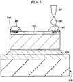
- Fig. 5 is a diagram schematically illustrating a forming process of the high electric field resistance sealing member MR.
- the semiconductor chip CHP is loaded on an insulated substrate SUB with a soldering material (an adhesive material) ADH and thereafter the high electric field resistance sealing member MR is formed over the region which strides over the anode electrode ADE from above the termination part TMR by dropping the high electric field resistance sealing member MR which is in a paste state from a dispenser DP. Thereafter, as illustrated in Fig.
- a wire W is connected to the anode electrode ADE which is formed on the front face of the semiconductor chip CHP and a silicone gel GL which is a sealing member is formed to cover the semiconductor chip CHP.
- a region AR the shape of an outer end part of the high electric filed resistance sealing member MR is formed into a hem-trailing tapered shape caused by a forming method in an application technology (a potting technology) performed after formation of the semiconductor chip illustrated in Fig. 5 . Consequently, the present inventers have newly found that, as illustrated in Fig.
- a film thickness of the high electric field resistance sealing member MR is thinned in the vicinity of the outer end part of the high electric field resistance sealing member MR and thereby it is not possible to sufficiently relax the electric field in the vicinity of an outer edge part of the semiconductor chip CHP. That is, the knowledge that the present inventers have newly found is knowledge that in the method of applying the pasted high electric field resistance sealing member MR onto the vicinity of the outer edge part of the semiconductor chip CHP by a potting method for the fragmented semiconductor chips CHP as in the related art, the film thickness of the outer end part of the high electric field resistance sealing member MR is thinned and it is not possible to sufficiently relax the electric field in this region. Consequently, an electric field whose intensity is more than the dielectric breakdown electric field intensity is imposed on the silicone gel and the reliability of the semiconductor device is lowered.
- the forming process of the high electric field resistance sealing member MR is performed after loading the fragmented semiconductor chip CHP on the insulated substrate SUB, for example, as illustrated in Fig. 5 .
- the high electric field resistance sealing member MR is applied by the dispenser DP to make one cycle along the termination part TMR of the semiconductor chip CHP which is loaded on the insulated substrate SUB via the soldering material ADH.
- thermosetting process of the high electric field resistance sealing member MR is necessary and, in the thermosetting process, it is necessary to heat-treat the insulated substrate SUB for several hours.
- the semiconductor chip CHP is soldered to the insulated substrate SUB with the soldering material ADH, the soldering material ADH is liquefied in reflow and a variation in thickness and movement and rotation in a horizontal direction occur.
- the present inventers newly find the room for improvement which is present in the related art and make a contrivance to the room for improvement.
- the technical idea in the present first embodiment that this contrivance is made will be described.
- the technical idea in the present first embodiment has a technical idea on a sectional view point and a technical idea on a planar view point, first, the technical idea focusing on the sectional view point will be described and then the technical idea focusing on the planar view point will be described.
- Fig. 7 is a sectional diagram schematically illustrating a semiconductor device SA1 in the present first embodiment, not forming part of the invention but useful for understanding it.
- a semiconductor chip CHP1 is loaded on the insulated substrate SUB via the soldering material ADH.
- the SiC device is formed on this semiconductor chip CHP1 and the diode is given as the SiC device in the present first embodiment particularly.
- a back-face electrode BE which functions as a cathode electrode of the diode is formed on a back face of the semiconductor chip CHP1.
- a front face of the semiconductor chip CHP1 is an element formation face.
- the anode electrode ADE of the diode is formed on the front face of the semiconductor chip CHP1 and the termination part TMR is formed to surround the anode electrode ADE.
- the termination part TMR is formed over a peripheral edge part of the semiconductor chip CHP1 and is formed for the purpose of relaxing the strength of the electric field on the peripheral edge part of the semiconductor chip CHP1.
- the diode which is the SiC device is formed on the inner side of the termination part TMR.
- the semiconductor chip CHP1 in the present first embodiment has a semiconductor element formation part that the diode is formed on the inner side of the peripheral edge part on which the termination part TMR is formed. Then, the high electric field resistance sealing member MR is formed to cover the termination part TMR which is formed on the peripheral edge part of the semiconductor chip CHP1 and to cover the vicinity of an end part of the anode electrode ADE. In addition, the wire W is connected to the vicinity of a central part of the anode electrode ADE.
- the semiconductor chip CHP1 so configured is sealed with the silicone gel GL which is the sealing member.
- the dielectric breakdown electric field intensity of the high electric field resistance sealing member MR becomes larger than the dielectric breakdown electric field intensity of the silicone gel GL which is the sealing member.
- the high electric field resistance sealing member MR is formed to cover only the vicinity of the peripheral edge part of the semiconductor chip CHP1 and is smaller in size than the silicone gel GL which is formed to cover the semiconductor chip CHP1. That is, a volume of the high electric field resistance sealing member MR is made smaller than a volume of the silicone gel GL which is the sealing member.
- the high electric field resistance sealing member MR is in direct contact with the silicone gel GL.
- the high electric field resistance sealing member MR is interposed between the termination part TMR which is formed on the peripheral edge part of the semiconductor chip CHP1 and the silicone gel GL. That is, an upper face of the termination part TMR is covered with the high electric field resistance sealing member MR and the termination part TMR is not in direct contact with the silicone gel GL.
- the semiconductor device SA1 in the present first embodiment contains the semiconductor material which is larger than silicon in band gap (silicon carbide, gallium nitride, diamond and so forth) and is equipped with the semiconductor chip CHP1 having the high electric field resistance sealing member MR (an insulating member) which covers the peripheral edge part of the element formation face and the silicone gel GL which is the sealing member for covering the semiconductor chip CHP1.
- the semiconductor chip CHP1 and an outer end face of the high electric field resistance sealing member MR include parts which are flush with each other.
- the high electric field resistance sealing member MR in the present first embodiment has a shape that a thickness of the outer end part of the high electric field resistance sealing member MR is thicker than thicknesses of other parts of the high electric field resistance sealing member MR.
- the high electric field resistance sealing member MR is configured by a material which is higher than the silicone gel GL in dielectric breakdown electric field intensity and may be configured by any of, for example, a polyimide resin, a polyamide-imide resin, a polyether-amide-imide resin and a polyether-amide resin.
- the semiconductor device SA1 in the present first embodiment is configured as described above. In the following, a manufacturing method thereof will be described with reference to the drawings . First, a flow of a manufacturing process of the semiconductor device SA1 in the present first embodiment will be described and thereafter details of the manufacturing process will be described with reference to a flowchart.
- Fig. 8 is a flowchart illustrating the flow of the manufacturing process of the semiconductor device SA1 in the present first embodiment.
- a semiconductor wafer which is configured by the semiconductor material (SiC) which is larger than silicon in band gap and has the element formation face is prepared.
- the semiconductor wafer has a plurality of chip regions, each of the chip regions which are present on the semiconductor wafer has the semiconductor element formation part and the peripheral edge part which surrounds the semiconductor element formation part, the diode which is the SiC device is formed on the semiconductor element formation part and the termination part is formed on the peripheral edge part.
- the high electric field resistance sealing member is formed to cover the termination part formed on the peripheral edge part of each chip region in a state of the semiconductor wafer (S101). Thereafter, testing of the SiC device formed in each chip region is performed in the state of the semiconductor wafer (S102). Then, the plurality of semiconductor chips are acquired by dicing the plurality of chip regions present on the semiconductor wafer (S103). Then, testing of the SiC devices formed on the semiconductor chips is performed in a state of the segmented semiconductor chips (S104). Next, the semiconductor chips are loaded on the substrate (the insulated substrate) (S105) and thereafter the semiconductor chips are electrically connected with the wires (wire bonding) (S106) . Then, the substrate with the semiconductor chips being loaded is disposed on a base plate (S107) and thereafter case assembling and the case is filled with the silicone gel which is the sealing member (S108). It is possible to manufacture the semiconductor device in the present first embodiment in this way.
- the pasted high electric field resistance sealing member MR is applied along a scribe line SCR which partitions chip regions CR in a state of a semiconductor wafer WF.
- the high electric field resistance sealing member MR is applied onto the semiconductor wafer WF by dropping the pasted high electric field resistance sealing member MR from the dispenser DP along the scribe line SCR which is present in the form of a grid.
- a resin which contains polyamide-imide as a principal component was used as the high electric field resistance sealing member MR.
- Characteristics were such that a viscosity of the high electric field resistance sealing member MR is 100 Pa ⁇ s and the dielectric breakdown electric filed intensity of the high electric filed resistance sealing member MR was 210 kV/mm which was at least ten times the dielectric breakdown electric field intensity of the silicone gel.
- Fig. 10 is a diagram illustrating part of the semiconductor wafer in an enlarged state and the four mutually adjacent chip regions CR are illustrated.
- the excessive high electric field intensity sealing member MR spreads out at a crossing place of a longitudinal direction with a lateral direction by performing application of the high electric field sealing member MR in the form of the grid along the scribe line SCR. Consequently, it is possible to effectively cover a corner part (a corner part) of the termination part TMR with the high electric field resistance sealing member MR.
- Fig. 11 is a sectional diagram illustrating a situation where the high electric field resistance sealing member MR is dropped from the dispenser DP to cover the termination part TMR formed on the semiconductor wafer WF. As illustrated in Fig. 11 , it is found that the pasted high electric field resistance sealing member MR which is dropped from the dispenser DP is formed to cover the termination part TMR and to cover the vicinity of the end part of the anode electrode which is disposed adjacent to the termination part TMR.
- heat treatment for curing the pasted high electric field resistance sealing member MR is performed.
- the heat treatment is continuously performed under conditions of a condition 1 (100°C, twenty minutes) and a condition 2 (200°C, one hour) and thereafter additional high-temperature heat treatment is performed under a condition of a condition 3 (an inert atmosphere, 300°C, one hour). It is possible to suppress occurrence of degassing from the high electric field resistance sealing member MR in high-temperature heat treatment (355°C in maximum) performed in a chip loading process which will be described later by this additional high-temperature heat treatment.
- a TDS device a temperature-programmed desorption gas analysis device.
- occurrence of degassing from the high electric field resistance sealing member MR is suppressed by imposing heat treatment at 200°C or higher which has not been performed so far on the high electric field resistance sealing member MR.
- a highest temperature for the heat treatment imposed on the high electric field resistance sealing member MR may be not more than a highest temperature in the chip loading process or less than a temperature at which pyrolysis of the high electric field resistance sealing member MR is started and is specifically not more than 400°C.
- the high electric field resistance sealing member MR is cured by the heat treatment and thereafter an electric characteristic inspection in a state of the semiconductor wafer WF is performed.
- the termination part TMR which is large in electric field intensity is covered with the high electric field resistance sealing member MR, discharge in the atmosphere is suppressed and consequently it is possible to perform a high-voltage application test with ease.
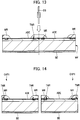
- FIG. 13 is a sectional diagram illustrating a situation of dicing the semiconductor wafer WF. As illustrated in Fig. 13 , the dicing is performed along a dotted line passing through the high electric field resistance sealing member MR and the termination part TMR. Thereby, as illustrated in Fig. 14 , the high electric field resistance sealing member MR and the termination part TMR are cut and the semiconductor wafer WF is segmented to the plurality of semiconductor chips CHP1.
- the electrical characteristic inspection is performed in the state of the semiconductor chips CHP1 and the semiconductor chip CHP1 which is a conforming article is sorted out. Thereafter, the semiconductor chip CHP1 is loaded on the substrate (the insulated substrate) (the chip loading process). At this time, since a high-melting-point soldering material is used for junction of the semiconductor chip CHP1 with the substrate, this chip loading process includes heat treatment performed at 355°C in maximum in a reducing atmosphere. Then, a wire bonding process of connecting a wire to the electrode (the anode electrode) of the semiconductor chip CHP1 which is joined to the substrate is performed.
- Fig. 15 is a sectional diagram illustrating the vicinity of the end part of the semiconductor chip CHP1 in the present first embodiment in an enlarged state.
- the back-face electrode BE which functions as the cathode electrode of the diode is formed on the back face of the semiconductor chip CHP1.
- the anode electrode ADE of the diode and the termination part TMR which is formed in a region on the outer side of the anode electrode ADE are formed on the front face of the semiconductor chip CHP1.
- This termination part TMR has a p-type semiconductor region PR1 which is formed in the semiconductor chip CHP1 and a p-type semiconductor region PR2 which enfolds the p-type semiconductor region PR1 and is lower in impurity concentration than the p-type semiconductor region PR1.
- the termination part TMR has an n-type semiconductor region NR which is formed separately from the p-type semiconductor region PR2 toward the end-face side of the semiconductor chip CHP1 and a channel stop layer CS which is formed on the n-type semiconductor region NR.
- the termination part TMR has a silicon oxide film OXF which extends from above the p-type semiconductor region PR1 and the p-type semiconductor region PR2 to reach the channel stop layer CS and a polyimide resin film PIF which covers the silicon oxide film OXF and the channel stop layer CS which projects from the silicon oxide film OXF.
- the polyimide resin film PIF functions as a protection film and has a film thickness of, for example, 4 ⁇ m to 9 ⁇ m.
- the termination part TMR configured in his way, since the p-type semiconductor region PR1 which is high in impurity concentration is enfolded with the p-type semiconductor region PR2 which is low in impurity concentration, it is possible to relax the electric field on the termination part TMR. Then, as illustrated in Fig. 15 , the high electric field resistance sealing member MR is formed to cover the termination part TMR. Although not illustrated in Fig. 15 , for example, as illustrated in Fig. 17 , the silicone gel GL is formed to cover the semiconductor chip CHP1 with the high electric field resistance sealing member MR formed. The electric field from the semiconductor chip CHP1 is applied to this silicone gel GL.
- a film thickness of the high electric field resistance sealing member MR which is formed on the termination part TMR be, for example, at least not less than 50 ⁇ m and be desirably not less than 80 ⁇ m in order to make the electric field intensity of the electric field applied to the silicone gel GL not exceed the dielectric breakdown electric field intensity (14 kV/mm) of the silicone gel GL.
- the film thickness of the high electric field resistance sealing member MR be not more than 500 ⁇ m because when it is too thick, a stress is increased and an issue of cracks and so forth becomes apparent.
- the semiconductor chip CHP1 in the present first embodiment a high withstand voltage product of, for example, 3.3 kV in withstand voltage is targeted.
- the semiconductor chip CHP1 in the present first embodiment is also applicable to medium withstand voltage products of 1.7 kV and 1.2 kV.
- it depends on the design of the termination part TMR it is possible to make a lower limit value of the film thickness of the high electric field resistance sealing member MR small and, for example, it is possible to set the film thickness of the high electric field resistance sealing member MR to 20 ⁇ m or more.
- a relative dielectric constant of the polyimide film PIF is about 2.9
- a relative dielectric constant of the polyether-amide resin which is a principal component which configures the high electric field resistance sealing member MR is about 3.2 and both are smaller than a relative dielectric constant (3.8 to 4.1) of the underlying silicon oxide film OXF.
- a relative dielectric constant of the silicone gel GL is about 2.7 and the relative dielectric constant of the polyimide film PIF and the relative dielectric constant of the high electric field resistance sealing member MR are larger than the relative dielectric constant of the silicone gel GL.
- a first characteristic point of the present first embodiment lies in the point that, for example, as illustrated in Fig. 15 , an end face EG1 of the semiconductor chip CHP1 and an outer end part EG2 of the high electric field resistance sealing member MR are configured to include parts which are flush with each other.
- an end face EG1 of the semiconductor chip CHP1 and an outer end part EG2 of the high electric field resistance sealing member MR are configured to include parts which are flush with each other.
- the outer end part of the high electric field resistance sealing member MR is formed to trail the hem, it follows that it is configured in such a manner that the end face of the semiconductor chip CHP and the outer end part of the high electric field resistance sealing member MR do not include the parts which are flush with each other. Consequently, in the related art illustrated in Fig. 6 , it becomes difficult to form the high electric field resistance sealing member MR on the vicinity of the end face of the semiconductor chip CHP which is high in electric field intensity. This means that the silicone gel GL is brought into direct contact with the vicinity of the end face of the semiconductor chip CHP which is high in electric field intensity.
- the silicone gel GL which is more liable to undergo dielectric breakdown than the high electric field resistance sealing member MR is brought into direct contact with the vicinity of the end face of the semiconductor chip CHP which is high in electric field intensity, the silicone gel GL is liable to undergo dielectric breakdown in the vicinity of the end face of the semiconductor chip CHP.
- the intensity of the electric field imposed onto the silicone gel GL in the vicinity of the end face of the semiconductor chip CHP exceeds the dielectric breakdown electric field intensity of the silicone gel GL and therefore the fear that the dielectric breakdown of the silicone gel GL may occur is increased. Accordingly, in the related art, the dielectric breakdown of the silicone gel GL is liable to occur due to the difficulty in forming the high electric field resistance sealing member MR in the vicinity of the end face of the semiconductor chip CHP which is high in electric field intensity and thereby the reliability of the semiconductor device is lowered.
- the end face of the semiconductor chip CHP1 and the outer end part of the high electric field resistance sealing member MR are configured to include the parts which are flush with each other.
- the high electric field resistance sealing member MR which is thick in film thickness is formed in the vicinity of the end face of the semiconductor chip CHP1 which is high in electric field intensity, it is possible to sufficiently relax the electric field intensity. Consequently, according to the preset first embodiment, it is possible to effectively suppress that the intensity of the electric field imposed on the silicone gel GL which is formed on the high electric field resistance sealing member MR which is thick in film thickness exceeds the dielectric breakdown electric field intensity of the silicone gel GL and thereby it is possible to effectively suppress the dielectric breakdown of the silicone gel GL.
- the present first embodiment since it is possible to interpose the high electric field resistance sealing member MR which is thick in film thickness between the semiconductor chip CHP1 and the silicone gel GL in the vicinity of the end part of the semiconductor chip CHP1, it is possible to effectively suppress the dielectric breakdown of the silicone gel GL. Therefore, according to the first characteristic point of the present first embodiment, it is possible to suppress a reduction in reliability of the semiconductor device caused by the dielectric breakdown of the silicone gel GL. In other words, according to the first characteristic point of the present first embodiment, it is possible to improve the reliability of the semiconductor device by forming the high electric field resistance sealing member MR which is thick in film thickness in the vicinity of the end face of the semiconductor chip CHP1 which is high in electric field intensity.
- the high electric field resistance sealing member MR which is thick in film thickness in the vicinity of the end face of the semiconductor chip CHP1 which is high in electric field intensity
- a design that the electric field intensity in the semiconductor chip CHP1 is enhanced becomes sufficiently possible. That is, according to the present first embodiment, it is possible to sufficiently realize a design which makes use of the excellent material characteristics of SiC. Specifically, also a design that the width of the termination part TMR is made small in such a manner that a high electric field is extended up to the vicinity of the end face of the semiconductor chip CHP1 also becomes possible.
- the design that the high electric field is extended up to the vicinity of the end face of the semiconductor chip CHP1 becomes possible and consequently it becomes possible to make the size of the termination part TMR which does not function as the element formation part small. From this, as the indirect effect of the first characteristic point of the preset first embodiment, it is possible to reduce the size of the semiconductor chip CHP1 and thereby it becomes possible to reduce the manufacturing cost of the semiconductor device.
- the first characteristic point of the present first embodiment is that, for example, as illustrated in Fig. 15 , the end face EG1 of the semiconductor chip CHP1 and the outer end part EG2 of the high electric field resistance sealing member MR may be configured to include the portions which are flush with each other. A portion which is not flush may be partially present on the outer end part EG2 of the high electric field resistance sealing member MR, for example, like a shape (an oblique shape) of a portion surrounded by a region CR illustrated in Fig. 16 and a shape (a projected shape) of a portion surrounded by a region DR illustrated in Fig. 17 .
- the first characteristic point of the present first embodiment is, the end face EG1 of the semiconductor chip CHP1 and the outer end part EG2 of the high electric field resistance sealing member MY may include portions which are at least partially flush with each other. Realization of this configuration leads to formation of the high electric filed resistance sealing member MR in the vicinity of the end face of the semiconductor chip CHP1 which is high in electric field intensity and it is possible to sufficiently obtain an electric filed relaxation effect by the high electric field resistance sealing member MR in the vicinity of the end face of the semiconductor chip CHP1.
- a second characteristic point of the present first embodiment lies in the point that, for example, as illustrated in Fig. 15 , a thickness of the outer end part EG2 of the high electric field resistance sealing member MR is made thicker than thicknesses of other parts of the high electric field resistance sealing member MR.
- the second characteristic point of the present first embodiment is embodied as a configuration that a film thickness of an inner end part EG3 of the high electric field resistance sealing member MR is gradually thinned, for example, as illustrated in Fig. 15 .
- the second characteristic point of the present first embodiment is that the shape of the inner end part EG3 of the high electric field resistance sealing member MR is in the form of a gently tapered shape.
- the present first embodiment it is possible to make a contact area between the semiconductor chip CHP1 and the high electric field resistance sealing member MR large. This means that it is possible to improve adhesive strength between the semiconductor chip CHP1 and the high electric field resistance sealing member MR and thereby it is possible to improve the reliability of the semiconductor device. Further, according to the second characteristic point of the present first embodiment, it is possible to cover not only the termination part TMR but also a peripheral region which is adjacent to the termination part TMR with the high electric field resistance sealing member MR.
- the second characteristic point of the present first embodiment it is possible to promote relaxation of the electric field intensity by the high electric field resistance sealing member MR not only on the termination part TMR but also on the peripheral region which is adjacent to the termination part TMR and, also from this point, it is possible to promote improvement of the reliability of the semiconductor device. That is, according to the second characteristic point of the present first embodiment, it is possible to realize improvement of the adhesive strength between the high electric field resistance sealing member MR and the semiconductor chip CHP1 and expansion of an electric field relaxation region owing to expansion of the region of the semiconductor chip CHP1 which is covered with the high electric field resistance sealing member MR.
- the anode electrode ADE works as an equipotential surface, the electric field from the termination part TMR spreads out centering on a boundary region between the termination part TMR and the anode electrode ADE.
- the shape of the inner end part EG3 of the high electric field resistance sealing member MR is in the form of the gently tapered shape, it follows that the high electric field resistance sealing member MR is formed to cover within a fixed distance range centering on the boundary region between the termination part TMR and the anode electrode ADE.
- the high electric field resistance sealing member MR is formed to correspond to the electric field which spreads out centering on the boundary region between the termination part TMR and the anode electrode ADE and it becomes possible to realize the electric field relaxation effect by the high electric field resistance sealing member MR without waste. Consequently, according to the second characteristic point of the present first embodiment, it is possible to cover a region which becomes high in electric field intensity with the high electric field resistance sealing member MR.
- the present first embodiment it is possible to suppress that the intensity of the electric field imposed on the silicone gel GL exceeds the dielectric breakdown electric field intensity of the silicone gel GL not only on the outer end part EG2 of the high electric field resistance sealing member MR but also on the inner end part EG3 of the high electric field resistance sealing member MR and thereby it is possible to effectively suppress the dielectric breakdown of the silicone gel GL.
- the second characteristic point of the present first embodiment it is also possible to obtain an advantage in a manufacturing method. That is, for example, as illustrated in Fig. 7 , even in a case where a junction between the anode electrode ADE of the semiconductor chip CHP1 and the wire W approaches the boundary region between the anode electrode ADE and the termination part TMR due to positional displacement occurred in wire bonding, when the inner end part EG3 of the high electric field resistance sealing member MR has the tapered shape, interference with a heel rising part of the junction is hard to occur. Thereby, it is possible to suppress damage to the high electric field resistance sealing member MR caused by the interference.
- the tapered shape of the inner end part of the high electric field resistance sealing member MR is automatically determined in accordance with an application condition under which the pasted high electric field resistance sealing member MR is applied and a patterning process for forming the inner end part of the high electric field resistance sealing member MR into the tapered shape becomes unnecessary.
- a patterning process for forming the inner end part of the high electric field resistance sealing member MR into the tapered shape becomes unnecessary.
- the film thickness of the high electric field resistance sealing member MR is as very thick as about 80 ⁇ m typically, the advantage that the patterning process for forming the inner end part of the high electric field resistance sealing member MR into the tapered shape is unnecessary in the present embodiment 1 becomes significant when considering that a general photolithography process which is applied to a film of up to 10 ⁇ m at most is difficult.
- an application condition under which the pasted high electric field resistance sealing member MR is applied in a range that desirable applied film thickness and application line width are obtained by using a nozzle diameter, a discharge pressure, a gap length (a distance between a nozzle and an application object), an application speed (an in-plane moving speed of the nozzle) of the dispenser and a viscosity and a temperature of the high electric field resistance sealing member MR as an application material as parameters.
- a third characteristic point of the present first embodiment lies in the point that the high electric field resistance sealing member MR is not formed for each of the segmented semiconductor chips CHP1 and the high electric field resistance sealing members MR are formed in the lump in the state of the semiconductor wafer before segmented into the semiconductor chips CHP1.
- the pasted high electric field resistance sealing member MR is applied along the scribe lines SCR of the semiconductor wafer WF and thereafter, as illustrated in Fig. 12 , the semiconductor wafer WF is diced along the scribe lines SCR. Thereby, it is possible to obtain the semiconductor chip CHP of the sectional shape as illustrated in Fig. 15 .
- the semiconductor chip CHP1 having the above-described first characteristic point.
- the outer end part EG2 of the high electric field resistance sealing member MR is formed into an almost vertical shape and a state where the film thickness is almost maximized is retained on the outer end part EG2 of the high electric field resistance sealing member MR.
- the third characteristic point of the present first embodiment it is possible to realize the first characteristic point of the present first embodiment that it is possible to thicken the film thickness of the high electric field resistance sealing member MR on the vicinity of the end face of the semiconductor chip CHP1. From this, according to the third characteristic point of the present first embodiment, it is possible to realize the shape of the high electric field resistance sealing member MR which makes effective suppression of the dielectric breakdown of the silicone gel GL possible and consequently it is possible to improve the reliability of the semiconductor device.
- the design that the high electric field is imposed up to the vicinity of the end part of the semiconductor chip CHP1 becomes possible by adopting the semiconductor device manufacturing method having the third characteristic point of the present first embodiment and consequently it becomes possible to make the size of the termination part TMR which does not function as the element formation part small. Therefore, according to the third characteristic point of the present first embodiment, it is possible to reduce the size of the semiconductor chip CHP1 and thereby it is possible to reduce the manufacturing cost of the semiconductor device.
- the shape of the high electric field resistance sealing member MR at least part of the outer end part EG2 of the high electric field resistance sealing member MR has a vertical or nearly vertical end-part shape and thereby sealing corresponding to the structure of the semiconductor chip CHP1 that the high electric field is attained in the vicinity of the end face of the semiconductor chip CHP1 becomes possible.
- the shape of the high electric field resistance sealing member MR is, even in a case where part of an upper part of the outer end part is formed into an inclined shape as illustrated in Fig. 16 and even in a case where the part of the upper part of the outer end part is formed into a projected shape as illustrated in Fig. 17 , it is possible to obtain the effect which is similar to that of the structure illustrated in Fig. 15 .
- Fig. 16 and Fig. 17 are determined mainly in accordance with a relation between the strength of a thermosetting condition of the high electric field sealing member MR and a dicing condition (blade rotation speed and moving velocity), it is possible to optimize it by taking other factors such as adhesiveness between the high electric field resistance sealing member MR and the semiconductor chip CHP1 and so forth after dicing into consideration.
- the third characteristic point of the present first embodiment it is possible to obtain advantages described in the following. That is, in the method of applying the high electric field resistance sealing member MR onto every semiconductor chip CHP loaded on the insulated substrate SUB as in the related art illustrated in Fig. 5 , there exist alignment deviations of inclination, in-plane position, rotation and so forth of the semiconductor chip CHP due to a variation in soldering material ADH used to adhere the semiconductor chips CHP to the insulated substrate SUB. From this, a highly accurate position correcting technology becomes necessary for the dispenser DP used for application of the high electric field resistance sealing member MR.
- the third characteristic point of the present first embodiment it is possible to reduce the cost of an application device and it is possible to reduce time taken for image recognition in a process of applying the high electric field resistance sealing member MR and time taken for movement of the nozzle for every semiconductor chip, it is possible to obtain a manufacturing time reduction effect.
- the high electric field resistance sealing member MR is not formed for every segmented semiconductor chip CHP1 and it is possible to form the high electric field resistance sealing members MR in the lump in the state of the semiconductor wafer WF before segmented into the semiconductor chips CHP1, it is possible to reduce TAT (turn-around time) of the manufacturing process. Simultaneously therewith, since the high electric field resistance sealing member MR is applied in the state of the semiconductor wafer that inclinations of the respective chip regions match one another at equal intervals, it is possible to improve also accuracy of a forming process and an inspection process of the high electric field sealing member MR. Thereby, according to the present first embodiment, it is possible to promote a reduction in disposal cost caused by defective formation of the high electric field resistance sealing member MR, simplification of the inspection process and price reduction of devices such as the dispenser and so forth.
- a withstand voltage inspection of the semiconductor wafer is facilitated by forming the high electric field resistance sealing member MR in the state of the semiconductor wafer.
- the high electric field resistance sealing member MR is not formed on the semiconductor wafer at the stage of the semiconductor wafer. From this, in the related art, it follows that the withstand voltage inspection is performed on the semiconductor wafer which is in a state where the high electric field resistance sealing member MR is not formed.
- the semiconductor device manufacturing method in the present first embodiment that the high electric field resistance sealing member MR is formed in the state of the semiconductor wafer, it follows that the high-temperature heat treatment which is performed in the chip loading process of loading the semiconductor chips on the insulated substrate is also imposed on the high electric field resistance sealing member MR. Accordingly, in the semiconductor device manufacturing method in the present first embodiment, it is feared that the issue of degassing from the high electric field resistance sealing member MR caused by imposition of the above-described high-temperature heat treatment on the high electric field resistance sealing member MR may become apparent.
- the on-resistance reduction and improvement of the withstand voltage are requested to the power semiconductor element, the on-resistance reduction and the improvement of the withstand voltage are in a trade-off relation.
- a corner part (a corner part) of the active region becomes higher in electric field than a side.
- the termination part is formed to surround the active region, a reduction in withstand voltage occurs on the corner part and it is feared that the power semiconductor element may be destroyed. From this, for example, it is conducted to form the corner part of the active region into an arc shape and thereby to relax the electric field on the corner part and to secure the withstand voltage.
- Fig. 18 is a plan view illustrating the semiconductor chip CHP in the related art.
- the semiconductor chip CHP in the related art is, the termination part TMR configured by the p-type semiconductor region PR1, the p-type semiconductor region PR2 and the channel stop layer CS is formed to surround the anode electrode ADE formed on the active region.
- the high electric field resistance sealing member MR is formed to cover the termination part TMR of the semiconductor chip CHP in the related art configured as illustrated in Fig. 18 .
- the high electric field resistance sealing member MR is formed in conformity to the shape of the corner part of the large radius of curvature, since the high electric field resistance sealing member which conforms to the shape of the corner part of the large radius of curvature is also formed on the corner part of the small radius of curvature, the area of the anode electrode ADE (corresponding to the active region) is reduced. This means that a region where the wire is formed on the anode electrode ADE becomes small.
- a fourth characteristic point of the present invention is the point that in a planar view, the shape of the inner end part of the high electric field resistance sealing member MR includes curved-line parts which are mutually different in radius of curvature.
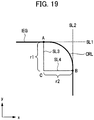
- Fig. 19 is a diagram illustrating the definition of the "radius of curvature” in the present invention.
- a thick line indicates an inner end part IEG of the high electric field resistance sealing member and the corner part is in the form of a curved-line part CRL.
- a straight line which extends from the inner end part IEG in an x-direction is set as a tangential line SL1 and a straight line which extends from the inner end part IEG in a y-direction is set as a tangential line SL2.
- a point at which the tangential line SL1 is separated from the inner end part IEG is set as a point A and a point at which the tangential line SL2 is separated from the inner end part IEG is set as a point B.
- a line segment which is drawn from the point A vertically relative to the tangential line SL1 is set as a line segment SL3 and a line segment which is drawn from the point B vertically relative to the tangential line SL2 is set as a line segment SL4.
- a length between the point A and the point C is designated by "r1" and a length between the point B and the point C is designated by "r2".
- the "radius of curvature” in the present first embodiment is defined as a mean value of "r1” and "r2". That is, the "radius of curvature” of the curved-line part CRL which configures the inner end part IEG of the high electric field resistance sealing member MR in the present first embodiment has the mean value of "r1" and "r2".
- Fig. 20(a) is a schematic diagram illustrating a planar configuration of the semiconductor chip CHP1 in the present invention.
- the semiconductor chip CHP1 in the present first embodiment has a rectangular shape
- the peripheral edge part of the semiconductor chip CHP1 is covered with the high electric field resistance sealing member MR and the anode electrode ADE which is formed on the central part of the semiconductor chip CHP1 is exposed from the high electric field resistance sealing member MR.
- the fourth characteristic point of the present first embodiment lies in the point that in the planar view, the shape of the inner end part IEG of the high electric field resistance sealing member MR includes curved-line parts which are mutually different in radius of curvature. Specifically, as illustrated in Fig.
- the radiuses of curvature of curved-line parts (CRL1A, CRL1B) formed on two corner parts in four corner parts are made larger than the radiuses of curvature of curved-line parts (CRL2A, CRL2B) formed on other two corner parts. That is, in the planar view, the shape of the inner end part IEG of the high electric field resistance sealing member MR includes one pair of the curved-line parts (CRL1A, CRL1B) having a first radius of curvature and one pair of the curved-line parts (CRL2A, CRL2B) having a second radius of curvature. Describing in more detail, for example, in Fig.
- one pair of diagonal lines of the rectangular semiconductor chip CHP1 are set as a diagonal line DGL1 and a diagonal line DGL2.
- one curved-line part CRL1A in one pair of the curved-line parts (CRL1A, CRL1B) intersects with the diagonal line DGL1
- one curved-line part CRL2B in one pair of the curved-line parts (CRL2A, CRL2B) intersects with the diagonal line DGL1.
- the other curved-line part CRL1B in one pair of the curved-line parts intersects with the diagonal line DGL2 and the other curved-line part CRL2A in one pair of the curved-line parts (CRL2A, CRL2B) intersects with the diagonal line DGL2.
- the planar termination part TMR illustrated in Fig. 18 with, for example, the planar high electric field resistance sealing member MR illustrated in Fig. 20(a) in just proportions. That is, according to the present invention, formation of the high electric field resistance sealing member MR of the shape that the inner end part IEG includes the curved-line parts of the different radiuses of curvature becomes possible on the same semiconductor chip CHP1. Thereby, according to the present invention, since it is possible to cover a region which is necessary to be covered with the high electric field resistance sealing member MR surely with the high electric field resistance sealing member MR by covering the planar termination part TMR illustrated in Fig.
- the fourth characteristic point of the present first embodiment since it is possible to conform the shape of the inner end part IEG of the high electric field resistance sealing member MR to the shape which covers the planar termination part TMR illustrated in Fig. 18 in just proportions, it is possible to simultaneously attain the on-resistance reduction and the improvement of the withstand voltage. In this way, according to the fourth characteristic point of the present first embodiment, it becomes possible to maximize the advantage of the planar termination part TMR having the parts which are mutually different in radius of curvature as illustrated in Fig. 18 and it is possible to realize performance improvement and reliability improvement of the semiconductor device.
- the technical idea of the present invention is not limited to the planar configuration illustrated in Fig. 20(a) and it is also possible to realize, for example, a planar configuration illustrated in Fig. 20(b) .
- Fig. 20(b) one curved-line part CRL1B in one pair of the curved-line parts (CRL1A, CRL1B) intersects with the diagonal line DGL1 and one curved-line part CRL2A in one pair of the curved-line parts (CRL2A, CRL2B) intersects with the diagonal line DGL1.
- the other curved-line part CRL1A in one pair of the curved-line parts (CRL1A, CRL1B) intersects with the diagonal line DGL2 and the other curved-line part CRL2B in one pair of the curved-line parts (CRL2A, CRL2B) intersects with the diagonal line DGL2.
- the semiconductor device manufacturing method in the present first embodiment has a fifth characteristic point which will be described in the following, with the above-described third characteristic point that the high electric field resistance sealing member MR is not formed for each of the segmented semiconductor chips CHP1 and the high electric field resistance sealing members MR are formed in the lump in the state of the semiconductor wafer before segmented into the semiconductor chips CHP1 being set forth as a premise.
- the pasted high electric field resistance sealing member MR is applied in the form of juxtaposed lines along the x-direction (a first direction) of the semiconductor wafer WF and the pasted high electric field resistance sealing member MR is applied in the form of juxtaposed lines in the y-direction (a second direction) which is orthogonal to the x-direction while the high electric field resistance sealing member MR which is applied in the x-direction is in the pasted state before dried.
- the pasted high electric field resistance sealing member MR is cured by performing high-temperature heat treatment on the semiconductor wafer WF.
- the fifth characteristic point lies in the point that in the forming process of the high electric field resistance sealing members MR in the present first embodiment, the pasted high electric field resistance sealing member MR is applied in the form of the juxtaposed lines in the y-direction (the second direction) which is orthogonal to the x-direction while the high electric field resistance sealing member MR applied in the x-direction is in the pasted state before dried.
- the pasted high electric field resistance sealing member MR applied in the x-direction is dragged when the pasted high electric field resistance sealing member MR is applied in the y-direction on a part where the pasted high electric field resistance sealing member MR applied in the x-direction intersects with the pasted high electric field resistance sealing member MR applied in the y-direction. Consequently, the shape of the inner end part of the high electric field resistance sealing member MR is changed on a corner part of the intersection part and an increase in radius of curvature occurs.
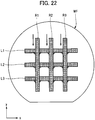
- Fig. 22 application of the pasted high electric field resistance sealing member MR in the y-direction has an influence on the shape of the inner end part the high electric field resistance sealing member MR and therefore is important.
- FIG. 22 three lines R1 to R3 obtained by performing application of three lines in the y-direction by the same-direction application from top to bottom are illustrated. Thereby, in intersection regions thereof with the three lines L1 to L3 formed by the application in the x-direction, the three lines L1 to L3 formed by the application in the x-direction are dragged downward and it is possible to form the high electric field resistance sealing member MR having the shape of the inner end part IEG illustrated in Fig. 20(a) .
- the three lines R1 to R3 are formed by performing application of the three lines in the y-direction by the same-direction application from bottom to top, in the intersection regions thereof with the three lines L1 to L3 formed by the application in the x-direction, the three lines L1 to L3 formed by the application in the x direction are dragged upward and it is possible to form the high electric field resistance sealing member MR having the shape of the inner end part IEG illustrated in Fig. 20(b) .
- the shape of the corner part of the inner end part of the high electric field resistance sealing member MR does not become right-angled and is in the form of a roundish shape which ordinarily has a certain radius of curvature and this roundish shape is caused by two factors peculiar to the present first embodiment which will be described in the following.
- a first factor is attributable to spontaneous spreading of the high electric field resistance sealing member MR applied onto the semiconductor wafer WF because it is in the pasted state when applied.
- the second factor is attributable to dragging of the pasted high electric field resistance sealing member MR firstly applied in the x-direction by the pasted high electric field resistance sealing member MR applied later in the y-direction which intersects with the x-direction while the high electric field resistance sealing member MR applied in the x-direction is in the pasted state in the intersection region when applying the pasted high electric field resistance sealing members MR onto the semiconductor wafer WF so as to intersect with each other vertically and horizontally.
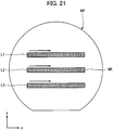
- FIG. 21 is a schematic diagram illustrating a situation of applying the pasted high electric field resistance sealing member MR onto the semiconductor wafer WF in the x-direction.
- the x-direction is a lateral direction when viewing the front face of the semiconductor wafer WF from above with an orientation flat part of the semiconductor wafer WF facing downward.
- the pasted high electric field resistance sealing member MR is applied at intervals of 6 mm and across a width of 1.9 mm by the dispenser that a condition is adjusted in such a manner that the film thickness of the high electric field resistance sealing member MR after finally cured reaches 80 ⁇ m.
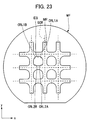
- Fig. 23 is a diagram schematically illustrating the high electric field resistance sealing member MR cured in a temperature sequence of (1) 100°C, twenty minutes, (2) 200°C, one hour and (3) 300°C, one hour under a nitrogen atmosphere in a state where the semiconductor wafer WF onto which the high electric field resistance sealing member MR illustrated in Fig. 22 is applied is held horizontally.
- the shape of the inner end part IEG of the high electric field resistance sealing member MR after cured includes the curved-line parts of the large radius of curvature (CRL1A, CRL1B) and the curved-line parts of the small radius of curvature (CRL2A, CRL2B).
- the shape of the inner end part of the high electric field resistance sealing member MR includes the curved-line parts which are mutually different in radius of curvature.
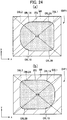
- Fig. 24(a) is a diagram schematically illustrating a planar configuration of the semiconductor chip CHP1 in a first modified example of the first embodiment.
- the semiconductor chip CHP1 in the first modified example has a rectangular shape, the peripheral edge part of the semiconductor chip CHP1 is covered with the high electric field resistance sealing member MR and the anode electrode ADE formed on the central part of the semiconductor chip CHP1 is exposed from the high electric field resistance sealing member MR.
- the semiconductor chip CHP1 in the first modified example has a rectangular shape
- the peripheral edge part of the semiconductor chip CHP1 is covered with the high electric field resistance sealing member MR and the anode electrode ADE formed on the central part of the semiconductor chip CHP1 is exposed from the high electric field resistance sealing member MR.
- the anode electrode ADE formed on the central part of the semiconductor chip CHP1 is exposed from the high electric field resistance sealing member MR.
- one pair of diagonal lines of the rectangular semiconductor chip CHP1 are the diagonal line DGL1 and the diagonal line DGL2.
- one curved-line part CRL1B in one pair of the curved-line lines intersects with the diagonal line DGL1 and one curved-line part CRL2A in one pair of the curved-line parts (CRL2A, CRL2B) intersects with the diagonal line DGL1.
- the other curved-line part CRL1A in one pair of the curved-line parts intersects with the diagonal line DGL2 and the other curved-line part CRL2B in one pair of the curved-line parts (CRL2A, CRL2B) intersects with the diagonal line DGL2.
- the shape of the inner end part IEG of the high electric field resistance sealing member MR is configured to include the curved-line parts which are mutually different in radius of curvature in this way.
- the semiconductor chip CHP1 in the present first modified example may have a planar configuration illustrated in Fig. 24(b) that left and right are reversed to the planar configuration illustrated in Fig. 24(a) , not limited to the planar configuration illustrated in Fig. 24 (a) .
- Fig. 24 (b) one curved-line part CRL1A in one pair of the curved-line parts (CRL1A, CRL1B) intersects with the diagonal line DGL1 and one curved-line part CRL2B in one pair of the curved-line parts (CRL2A, CRL2B) intersects with the diagonal line DGL1.
- the other curved-line part CRL1B in one pair of the curved-line parts intersects with the diagonal line DGL2 and the other curved-line part CRL2A in one pair of the curved-line parts (CRL2A, CRL2B) intersects with the diagonal line DGL2.
- the shape of the inner end part IEG of the high electric field resistance sealing member MR is configured to include the curved-line parts which are mutually different in radius of curvature.
- Fig. 25 is a diagram schematically illustrating a manufacturing process for realizing the shape of the inner end part IEG of the high electric field resistance sealing member MR illustrated in Fig. 24 (a) .
- First, as illustrated in Fig. 25 application of the pasted high electric field resistance sealing member MR in the y-direction is performed.
- the three lines R1 to R3 are illustrated.
- application of the pasted high electric field resistance sealing member MR in the x-direction is performed.
- the three lines L1 to L3 obtained by performing application of three lines in the x-direction by the same-direction application from left to right are illustrated.
- the three lines L1 to L3 are formed by performing application of three lines in the x-direction by the same-direction application from right to left, in intersection regions thereof with the three lines R1 to R3 formed by the application in the y-direction, the three lines R1 to R3 which are formed by the application in the y-direction are dragged leftwards and it is possible to form the high electric field resistance sealing member MR having the shape of the inner end part IEG illustrated in Fig. 24(b) .
- Fig. 27(a) is a diagram schematically illustrating a planar configuration of the semiconductor chip CHP1 in a second modified example of the first embodiment.
- each of one pair of the curved-line parts (CRL2A, CRL2B) intersects with the diagonal line DGL1 and each of one pair of the curved-line parts CRL1A, CRL1B) intersects with the diagonal line DGL2.
- the shape of the inner end part IEG of the high electric field resistance sealing member MR is configured to include the curved-line parts which are mutually different in radius of curvature.
- the semiconductor chip CHP1 in the present second modified example may have a planar configuration illustrated in Fig. 27(b) that left and right are reversed to the planar configuration illustrated in Fig. 27(a) , not limited to the planar configuration illustrated in Fig. 27(a) .
- each of one pair of the curved-line parts (CRL1A, CRL1B) intersects with the diagonal line DGL1 and each of one pair of the curved-line parts CRL2A, CRL2B) intersects with the diagonal line DGL2.
- the shape of the inner end part IEG of the high electric field resistance sealing member MR is configured to include the curved-line parts which are mutually different in radius of curvature.
- Fig. 28(a) is a schematic diagram illustrating a state where coupling parts CU1 to CU3 with the wires are formed on a front face of the anode electrode ADE formed on the element formation part in the semiconductor chip CHP1 having the planar configuration illustrated in Fig. 27(a) .
- the curved-line parts (CRL2A, CRL2B) having the small radius of curvature are formed to intersect with the diagonal line DGL1. Accordingly, the width of the anode electrode ADE along the diagonal line DGL1 is increased and consequently it is possible to dispose the plurality of coupling parts CU1 to CU3 of the semiconductor chip CHP1 with each of the plurality of wires along this diagonal line DGL1.
- a width L1 of the high electric field resistance sealing member MR which is a distance between a corner part CNR1 which is a one-end point of the diagonal line DGL1 and a cross-point CP1 of the curved-line part CRL2A with the diagonal line DGL1 is made smaller than a width L2 of the high electric field resistance sealing member MR which is a distance between a corner part CNR2 which is a one-end point of the diagonal line DGL2 and a cross-point CP2 of the curved-line part CRL1A with the diagonal line DGL2.
- the width L1 of the high electric field resistance sealing member MR along the diagonal line DGL1 becomes small and consequently it is possible to obtain an advantage that it becomes easy to dispose the plurality of connection parts CU1 to CU3 along the diagonal line DGL1 and the width L2 of the high electric field resistance sealing member MR along the diagonal line DGL2 becomes large and consequently it is possible to improve the withstand voltage.
- Fig. 28(b) is a schematic diagram illustrating a state where in the semiconductor chip CHP1 having the planar configuration illustrated in Fig. 27(b) , the connection parts CU1 to CU3 with the wires are formed on the front face of the anode electrode ADE formed on the element formation part.
- the curved-line parts of the small radius of curvature (CRL2A, CRL2B) are formed to intersect with the diagonal line DGL2. Accordingly, the width of the anode electrode ADE along the diagonal line DGL2 is increased and consequently it is possible to dispose the plurality of connection parts CU1 to CU3 of the semiconductor chip CHP1 with each of the plurality of wires.
- the shape of the inner end part IEG of the high electric field resistance sealing member MR is formed in such a manner that the radiuses of curvature of the curved-line parts (CRL2A, CRL2B) which intersect with diagonal line DGL2 become small and thereby it is possible to obtain an advantage that it becomes easy to dispose the plurality of coupling parts CU1 to CU3 along the diagonal line DGL2. In this case, it is easy to equalize the values of current flowing into the plurality of wires and it is possible to improve the reliability of the semiconductor device.
- Fig. 29 is a diagram schematically illustrating a manufacturing process for realizing the shape of the inner end part IEG of the high electric field resistance sealing member MR illustrated in Fig. 27 (a) .
- the three lines R1 to R3 are illustrated.
- application of the pasted high electric field resistance sealing member MR in the x-direction is performed.
- the three lines L1 to L3 obtained by performing application of three lines in the x-direction by the alternate application are illustrated.
- the three lines R1 to R3 formed by the application in the y-direction are dragged as illustrated in Fig. 29 and it is possible to form the high electric field resistance sealing member MR having the shape of the inner end part IEG illustrated in Fig. 27 (a) .
- the three lines L1 to L3 are formed by performing the application of three lines in the x-direction reversely to the case in Fig.
- the three lines R1 to R3 are dragged and it is possible to form the high electric field resistance sealing member MR having the shape of the inner end part IEG illustrated in Fig. 27(b) .
- Fig. 31 is a diagram illustrating specific examples of numerical values of respective parameters in regard to each of a plurality of chips 1 to 14 defined by the respective parameters.
- “Chip Lateral Dimension” indicates a lateral width of each chip and “Chip Longitudinal Dimension” indicates a longitudinal width of the chip.
- “Resin Width 1” indicates a dimension (a minimum part) (mm) which is one half the width of the high electric field resistance sealing member (a resin) applied in a lateral direction
- “Resin Width 2” indicates a dimension (the minimum part) which is one half the width of the high electric field resistance sealing member MR applied in a longitudinal direction.
- Resin Height 1 indicates a maximum thickness ( ⁇ m) of the high electric field resistance sealing member MR (the resin) applied in the lateral direction and "Resin Height 2" indicates a maximum thickness ( ⁇ m) of the high electric field resistance sealing member MR applied in the longitudinal direction.
- Each of "Inner Circumference Shapes A to F” indicates a shape illustrated in Fig. 31 .
- Each of “Radiuses of Curvatures 1 to 4" is a radius of curvature (mm) of a curved-line part surrounded by a broken line in Fig. 31 .
- FIG. 32 and Fig. 33 are schematic diagrams illustrating a configuration of a semiconductor module MJ in the present first embodiment.
- the plurality of semiconductor chips CHP1 in the present first embodiment with the diodes formed and a plurality of semiconductor chips CHP2 with the Si-IGBTs which function as switching elements formed are loaded on the insulated substrate SUB.
- Fig. 34 is a schematic diagram illustrating a planar configuration example of the insulated substrate SUB.
- the ten semiconductor chips CHP1 with the diodes (SiC devices) formed and the four semiconductor chips CHP2 with the Si-IGBTs formed are loaded on the insulated substrate SUB.
- a terminal is formed on a central part of the insulated substrate SUB, the terminal is electrically coupled with the plurality of semiconductor chips CHP1 via the wires and the terminal is electrically coupled with the plurality of semiconductor chips CHP2 via the wires.
- the insulated substrate SUB on which the plurality of semiconductor chips CHP1 and the plurality of semiconductor chips CHP2 are loaded is disposed on a base plate PLT which configures a lower face of a case CAS.
- the plurality of insulated substrates SUB are disposed on this base plate PLT.
- the insulated substrate SUB disposed on the base plate PLT is coupled with a member (a heat radiation member, a coupling member) PAT.
- the member PAT is coupled with a cap CAP which is a lid of the case CAS.
- an inner space of the case CAS is sealed with, for example, the silicone gel (the sealing member).
- the semiconductor module MJ in the present first embodiment is configured. It becomes possible to realize the power conversion device represented by the inverter and the converter by combining the plurality of semiconductor modules MJ in the present first embodiment with one another.
- Fig. 35 is a diagram illustrating a planar configuration of a semiconductor chip CHP3 with the SiC-MOSFET formed.
- the semiconductor chip CHP3 has a rectangular shape, a gate pad GP is disposed on its central part, and a source pad SP is disposed to surround this gate pad GP and the termination part TMR is disposed to surround the source pad SP. Then, the high electric field resistance sealing member MR is formed to cover part of the source pad SP from the termination part TMR.
- the wire is coupled the source pad SP and the wire is also coupled to the gate pad GP.
- the gate pad GP since the gate pad GP is disposed on a central part of the source pad SP, the gate pad GP becomes an obstacle when coupling the source pad SP and the wire with each other.
- Fig. 36 is a diagram illustrating a semiconductor chip CHP4 of a planar configuration that the gate pad SP is disposed in the vicinity of the end part of the source pad SP.
- the gate pad GP is disposed deviating from the central part of the source pad SP to the + x-direction side.
- Fig. 37 (a) is a schematic diagram illustrating a planar configuration of the semiconductor chip CHP4 in the present second embodiment according to the present invention.
- the high electric field resistance sealing member MR is formed to surround the source pad SP and the inner end part IEG of this high electric field resistance sealing member MR is configured to include one pair of the curved-line parts (CRL1A, CRL1B) of the large radius of curvature and one pair of the curved-line parts (CRL2A, CRL2B) of the small radius of curvature.
- a characteristic point of the present second embodiment lies in the point that as illustrated in Fig. 37(a) , the gate pad GP is disposed at a position closer to one pair of the curved-line parts of the small radius of curvature (CRL2A, CRL2B) than to one pair of the curved-line parts of the large radius of curvature (CRL1A, CRL1B) .
- the gate pad GP is disposed at a position closer to one pair of the curved-line parts of the small radius of curvature (CRL2A, CRL2B) than to one pair of the curved-line parts of the large radius of curvature (CRL1A, CRL1B) .
- the semiconductor chip CHP4 in the present second embodiment may have a planar configuration illustrated in Fig. 37(b) that left and right are reversed to the planar configuration illustrated in Fig. 37(a) , not limited to the planar configuration illustrated in Fig. 37(a) .
- the gate pad GP is disposed in the vicinity of a left end part of the source pad SP.
- the semiconductor chip CHP4 in the present second embodiment may also have a planar configuration illustrated in Fig. 38(a) and a planar configuration illustrated in Fig. 38(b) , not limited to the planar configurations illustrated in Fig. 37(a) and Fig. 37(b) .
- Fig. 38(a) it follows that the gate pad GP is disposed in the vicinity of a lower end part of the source pad SP and in Fig. 38(b) , it follows that the gate pad GP is disposed in the vicinity of an upper end part of the source pad SP.
- Fig. 39 is a schematic diagram illustrating a planar configuration example of the insulated substrate SUB.
- the ten semiconductor chips CHP1 with the diodes (the SiC devices) formed and the four semiconductor chips CHP4 in the present second embodiment with the SiC-MOSFETs formed are loaded on the insulated substrate SUB.
- the terminal is formed on the central part of the insulated substrate SUB, the terminal is electrically coupled with the plurality of semiconductor chips CHP1 via the wires and the terminal is electrically coupled with the plurality of semiconductor chips CHP4 via the wires.
- the gate pads formed on the semiconductor chips CHP4 are electrically coupled with the terminal of the insulated substrate SUB via the wires and the source pads formed on the semiconductor chips CHP4 are electrically coupled with the terminal of the insulated substrate SUB via the wires.
- the gate pad is disposed in the vicinity of the end part of the source pad, it is possible to electrically couple the source pad with the terminal of the insulated substrate SUB without being hindered by the gate pad.
- the technical idea of the present second embodiment is also applicable to the SiC-IGBT having the gate pad similarly to the SiC-MOSFET, not limited to the SiC-MOSFET.
- the technical ideas of the aforementioned embodiments are applicable to, for example, an SiC hybrid module that the SiC-IGBT is combined with the SiC-diode (the SiC- Schottky barrier diode) and are also applicable to a full SiC module configured by the SiC-MOSFET and a full SiC module that the SiC-IGBT is combined with the SiC-diode. Further, the technical ideas of the aforementioned embodiments are also applicable to, for example, a technology of combining a semiconductor element using the wide band gap semiconductor material such as SiC, GaN, diamond and so forth with a semiconductor element using a semiconductor material which has a general band gap such as silicon, gallium arsenide, germanium and so forth.
- the technical ideas of the aforementioned embodiments are also applicable to a technology of combining semiconductor elements such as the Schottky barrier diode and the p-n junction diode, the MOSFET and a junction FET, the bipolar transistor, the IGBT and so forth with one another/each other.
Landscapes
- Structures Or Materials For Encapsulating Or Coating Semiconductor Devices Or Solid State Devices (AREA)
- Inverter Devices (AREA)
- Electrodes Of Semiconductors (AREA)
Claims (6)
- Halbleitervorrichtung, umfassend:einen Halbleiterchip (CHP), der ein Halbleitermaterial umfasst, dessen Bandlücke größer als jene von Silicium ist,wobei der Halbleiterchip (CHP) Folgendes aufweist:einen Umfangskantenteil;einen Halbleiterelementausbildungsteil, der auf einer Innenseite des Umfangskantenteils angeordnet ist; undeinen Isolierteil (MR), der den Umfangskantenteil bedeckt und den Halbleiterelementausbildungsteil umgibt, undwobei eine Form eines Innenendteils (IEG) des Isolierteils (MR) in einer Draufsicht gekrümmte-Linie-Teile (CRL1A, CRL1B, CRL2A, CRL2B) umfasst, die einen jeweils unterschiedlichen Krümmungsradius aufweisen,wobei die Form des Innenendteils (IEG) des Isolierteils (MR) in der Draufsicht Folgendes umfasst:ein Paar von ersten gekrümmte-Linie-Teilen (CRL1A, CRL1B), die einen ersten Krümmungsradius aufweisen; undein Paar von zweiten gekrümmte-Linie-Teilen (CRL2A, CRL2B), die einen zweiten Krümmungsradius aufweisen, der sich von dem ersten Krümmungsradius unterscheidet.
- Halbleitervorrichtung nach Anspruch 1,
wobei der Halbleiterchip (CHP) durch eine rechteckige Form konfiguriert ist, die eine erste Diagonallinie (DGL1) und eine zweite Diagonallinie (DGL2) aufweist,
wobei jeder des einen Paars der ersten gekrümmte-Linie-Teile (CRL1A, CRL1B) sich mit der zweiten Diagonallinie (DGL2) überschneidet, und
wobei jeder des einen Paars der zweiten gekrümmte-Linie-Teile (CRL2A, CRL2B) sich mit der ersten Diagonallinie (DGL1) überschneidet. - Halbleitervorrichtung nach Anspruch 2,
wobei der zweite Krümmungsradius kleiner als der erste Krümmungsradius ist und
eine Vielzahl von Verbindungsteilen (CU1, CU2, CU3) des Halbleiterchips (CHP) in einer Draufsicht mit jedem einer Vielzahl von Drähten auf dem Halbleiterelementausbildungsteil angeordnet sind, der von dem Isolierteil (MR) entlang der ersten Diagonallinie (DGL1) freiliegt. - Halbleitervorrichtung nach Anspruch 1,
wobei der Halbleiterchip (CHP) durch eine rechteckige Form konfiguriert ist, die eine erste Diagonallinie (DGL1) und eine zweite Diagonallinie (DGL2) aufweist,
wobei ein erster gekrümmte-Linie-Teil in dem einen Paar der ersten gekrümmte-Linie-Teile (CRL1A, CRL1B) sich mit der ersten Diagonallinie (DGL1) überschneidet,
wobei ein zweiter gekrümmte-Linie-Teil in dem einen Paar der zweiten gekrümmte-Linie-Teile (CRL2A, CRL2B) sich mit der ersten Diagonallinie (DGL1) überschneidet,
wobei der andere erste gekrümmte-Linie-Teil in dem einen Paar der ersten gekrümmte-Linie-Teile (CRL1A, CRL1B) sich mit der zweiten Diagonallinie (DGL2) überschneidet und
wobei der andere zweite gekrümmte-Linie-Teil in dem einen Paar der zweiten gekrümmte-Linie-Teile (CRL2A, CRL2B) sich mit der zweiten Diagonallinie (DGL2) überschneidet. - Halbleitervorrichtung nach Anspruch 4,
wobei eine Kontaktflächenelektrode (GP) eines Leistungstransistors auf dem Halbleiterelementausbildungsteil angeordnet ist,
wobei der zweite Krümmungsradius kleiner als der erste Krümmungsradius ist und
wobei die Kontaktflächenelektrode (GP) an einer Position angeordnet ist, die sich näher an dem einen Paar der zweiten gekrümmte-Linie-Teile (CRL2A, CRL2B) als an dem einen Paar der ersten gekrümmte-Linie-Teile (CRL1A, CRL1B) befindet. - Halbleitervorrichtung nach Anspruch 1,
wobei der Halbleiterchip (CHP) durch eine rechteckige Form konfiguriert ist, die eine erste Diagonallinie (DGL1) und eine zweite Diagonallinie (DGL2) aufweist,
wobei eine Form eines Innenendteils (IEG) des Isolierteils (MR) in einer Draufsicht Folgendes umfasst:einen ersten gekrümmte-Linie-Teil, der einen ersten Krümmungsradius aufweist und sich mit der zweiten Diagonallinie (DGL2) überschneidet, undeinen zweiten gekrümmte-Linie-Teil (CRL2A), der einen zweiten Krümmungsradius aufweist, der kleiner als der erste Krümmungsradius ist, und sich mit der ersten Diagonallinie (DGL1) überschneidet, undwobei eine erste Breite (L1) des Isolierteils (MR), die ein Abstand zwischen einem ersten Eckteil (CNR1), der ein Endpunkt der ersten Diagonallinie (DGL1) ist, und einem ersten Kreuzungspunkt (CP1) des zweiten gekrümmte-Linie-Teils (CRL2A) mit der ersten Diagonallinie (DGL1) ist, kleiner als eine zweite Breite (L2) des Isolierteils (MR) ist, die ein Abstand zwischen einem zweiten Eckteil (CNR2), der ein Endpunkt der zweiten Diagonallinie (DGL2) ist, und einem zweiten Kreuzungspunkt (CP2) des ersten gekrümmte-Linie-Teils (CRL1A) mit der zweiten Diagonallinie (DGL2) ist.
Applications Claiming Priority (1)
| Application Number | Priority Date | Filing Date | Title |
|---|---|---|---|
| PCT/JP2016/050128 WO2017119064A1 (ja) | 2016-01-05 | 2016-01-05 | 半導体装置 |
Publications (3)
| Publication Number | Publication Date |
|---|---|
| EP3401954A1 EP3401954A1 (de) | 2018-11-14 |
| EP3401954A4 EP3401954A4 (de) | 2019-12-04 |
| EP3401954B1 true EP3401954B1 (de) | 2020-05-06 |
Family
ID=59274501
Family Applications (1)
| Application Number | Title | Priority Date | Filing Date |
|---|---|---|---|
| EP16883569.2A Active EP3401954B1 (de) | 2016-01-05 | 2016-01-05 | Halbleiterbauelement |
Country Status (3)
| Country | Link |
|---|---|
| EP (1) | EP3401954B1 (de) |
| JP (1) | JP6457663B2 (de) |
| WO (1) | WO2017119064A1 (de) |
Families Citing this family (3)
| Publication number | Priority date | Publication date | Assignee | Title |
|---|---|---|---|---|
| JP2020191367A (ja) * | 2019-05-21 | 2020-11-26 | 株式会社デンソー | 半導体装置 |
| JP7461210B2 (ja) | 2020-05-14 | 2024-04-03 | 株式会社日立製作所 | 半導体装置の製造方法 |
| JP7541455B2 (ja) * | 2020-09-10 | 2024-08-28 | ローム株式会社 | 半導体装置 |
Family Cites Families (6)
| Publication number | Priority date | Publication date | Assignee | Title |
|---|---|---|---|---|
| JP5600698B2 (ja) * | 2012-03-14 | 2014-10-01 | 株式会社 日立パワーデバイス | SiC素子搭載パワー半導体モジュール |
| JP2013239488A (ja) * | 2012-05-11 | 2013-11-28 | Rohm Co Ltd | 半導体装置 |
| JP2013239607A (ja) * | 2012-05-16 | 2013-11-28 | Mitsubishi Electric Corp | 半導体装置 |
| JP5943819B2 (ja) * | 2012-11-30 | 2016-07-05 | 三菱電機株式会社 | 半導体素子、半導体装置 |
| JP2014236166A (ja) * | 2013-06-04 | 2014-12-15 | 株式会社 日立パワーデバイス | 半導体装置 |
| JP2015032665A (ja) * | 2013-08-01 | 2015-02-16 | 住友電気工業株式会社 | ワイドバンドギャップ半導体装置 |
-
2016
- 2016-01-05 EP EP16883569.2A patent/EP3401954B1/de active Active
- 2016-01-05 WO PCT/JP2016/050128 patent/WO2017119064A1/ja not_active Ceased
- 2016-01-05 JP JP2017559961A patent/JP6457663B2/ja active Active
Non-Patent Citations (1)
| Title |
|---|
| None * |
Also Published As
| Publication number | Publication date |
|---|---|
| JPWO2017119064A1 (ja) | 2018-05-31 |
| EP3401954A4 (de) | 2019-12-04 |
| EP3401954A1 (de) | 2018-11-14 |
| JP6457663B2 (ja) | 2019-01-23 |
| WO2017119064A1 (ja) | 2017-07-13 |
Similar Documents
| Publication | Publication Date | Title |
|---|---|---|
| JP7286715B2 (ja) | 半導体装置、半導体パッケージおよび電源装置 | |
| US10083948B2 (en) | Semiconductor device, method for manufacturing same, and semiconductor module | |
| WO2016162987A1 (ja) | 半導体装置および半導体モジュール | |
| US10147707B2 (en) | Semiconductor device | |
| EP2722879A1 (de) | Halbleitereinheit und halbleitervorrichtung damit | |
| US10109549B2 (en) | Semiconductor device and power conversion device using same | |
| EP3401954B1 (de) | Halbleiterbauelement | |
| WO2016016970A1 (ja) | 半導体装置、半導体装置の製造方法および電力変換装置 | |
| JP7823093B2 (ja) | 電界抑制が向上させられた高電圧半導体装置を製作する方法 | |
| TWI801570B (zh) | 半導體裝置及其製造方法 | |
| JP2017143185A (ja) | 半導体装置およびその製造方法 | |
| WO2015125281A1 (ja) | パワーモジュール、電力変換装置、および鉄道車両 | |
| JP6647151B2 (ja) | 半導体装置およびその製造方法並びに半導体モジュールおよび電力変換装置 | |
| KR102841841B1 (ko) | 전기장 억제가 개선된 고전압 반도체 디바이스 | |
| US11296191B2 (en) | Power module and power converter | |
| US12610785B2 (en) | Semiconductor device and method for manufacturing the same | |
| US20210296197A1 (en) | Semiconductor device | |
| US20260101814A1 (en) | Power Semiconductor Device Package |
Legal Events
| Date | Code | Title | Description |
|---|---|---|---|
| STAA | Information on the status of an ep patent application or granted ep patent |
Free format text: STATUS: THE INTERNATIONAL PUBLICATION HAS BEEN MADE |
|
| PUAI | Public reference made under article 153(3) epc to a published international application that has entered the european phase |
Free format text: ORIGINAL CODE: 0009012 |
|
| STAA | Information on the status of an ep patent application or granted ep patent |
Free format text: STATUS: REQUEST FOR EXAMINATION WAS MADE |
|
| 17P | Request for examination filed |
Effective date: 20180205 |
|
| AK | Designated contracting states |
Kind code of ref document: A1 Designated state(s): AL AT BE BG CH CY CZ DE DK EE ES FI FR GB GR HR HU IE IS IT LI LT LU LV MC MK MT NL NO PL PT RO RS SE SI SK SM TR |
|
| AX | Request for extension of the european patent |
Extension state: BA ME |
|
| DAV | Request for validation of the european patent (deleted) | ||
| DAX | Request for extension of the european patent (deleted) | ||
| RIC1 | Information provided on ipc code assigned before grant |
Ipc: H01L 23/31 20060101ALI20190801BHEP Ipc: H01L 25/07 20060101ALI20190801BHEP Ipc: H01L 23/29 20060101AFI20190801BHEP Ipc: H01L 25/18 20060101ALI20190801BHEP Ipc: H01L 23/28 20060101ALI20190801BHEP |
|
| A4 | Supplementary search report drawn up and despatched |
Effective date: 20191031 |
|
| RIC1 | Information provided on ipc code assigned before grant |
Ipc: H01L 21/56 20060101ALN20191025BHEP Ipc: H01L 23/31 20060101ALI20191025BHEP Ipc: H01L 23/29 20060101AFI20191025BHEP Ipc: H01L 23/28 20060101ALI20191025BHEP |
|
| GRAP | Despatch of communication of intention to grant a patent |
Free format text: ORIGINAL CODE: EPIDOSNIGR1 |
|
| STAA | Information on the status of an ep patent application or granted ep patent |
Free format text: STATUS: GRANT OF PATENT IS INTENDED |
|
| RIC1 | Information provided on ipc code assigned before grant |
Ipc: H01L 23/29 20060101AFI20200203BHEP Ipc: H01L 21/56 20060101ALN20200203BHEP Ipc: H01L 23/28 20060101ALI20200203BHEP Ipc: H01L 23/31 20060101ALI20200203BHEP |
|
| RIC1 | Information provided on ipc code assigned before grant |
Ipc: H01L 21/56 20060101ALN20200211BHEP Ipc: H01L 23/28 20060101ALI20200211BHEP Ipc: H01L 23/29 20060101AFI20200211BHEP Ipc: H01L 23/31 20060101ALI20200211BHEP |
|
| INTG | Intention to grant announced |
Effective date: 20200224 |
|
| GRAS | Grant fee paid |
Free format text: ORIGINAL CODE: EPIDOSNIGR3 |
|
| GRAA | (expected) grant |
Free format text: ORIGINAL CODE: 0009210 |
|
| STAA | Information on the status of an ep patent application or granted ep patent |
Free format text: STATUS: THE PATENT HAS BEEN GRANTED |
|
| AK | Designated contracting states |
Kind code of ref document: B1 Designated state(s): AL AT BE BG CH CY CZ DE DK EE ES FI FR GB GR HR HU IE IS IT LI LT LU LV MC MK MT NL NO PL PT RO RS SE SI SK SM TR |
|
| REG | Reference to a national code |
Ref country code: GB Ref legal event code: FG4D |
|
| REG | Reference to a national code |
Ref country code: AT Ref legal event code: REF Ref document number: 1268177 Country of ref document: AT Kind code of ref document: T Effective date: 20200515 Ref country code: CH Ref legal event code: EP |
|
| REG | Reference to a national code |
Ref country code: DE Ref legal event code: R096 Ref document number: 602016036206 Country of ref document: DE |
|
| REG | Reference to a national code |
Ref country code: IE Ref legal event code: FG4D |
|
| REG | Reference to a national code |
Ref country code: LT Ref legal event code: MG4D |
|
| REG | Reference to a national code |
Ref country code: NL Ref legal event code: MP Effective date: 20200506 |
|
| PG25 | Lapsed in a contracting state [announced via postgrant information from national office to epo] |
Ref country code: SE Free format text: LAPSE BECAUSE OF FAILURE TO SUBMIT A TRANSLATION OF THE DESCRIPTION OR TO PAY THE FEE WITHIN THE PRESCRIBED TIME-LIMIT Effective date: 20200506 Ref country code: GR Free format text: LAPSE BECAUSE OF FAILURE TO SUBMIT A TRANSLATION OF THE DESCRIPTION OR TO PAY THE FEE WITHIN THE PRESCRIBED TIME-LIMIT Effective date: 20200807 Ref country code: NO Free format text: LAPSE BECAUSE OF FAILURE TO SUBMIT A TRANSLATION OF THE DESCRIPTION OR TO PAY THE FEE WITHIN THE PRESCRIBED TIME-LIMIT Effective date: 20200806 Ref country code: LT Free format text: LAPSE BECAUSE OF FAILURE TO SUBMIT A TRANSLATION OF THE DESCRIPTION OR TO PAY THE FEE WITHIN THE PRESCRIBED TIME-LIMIT Effective date: 20200506 Ref country code: FI Free format text: LAPSE BECAUSE OF FAILURE TO SUBMIT A TRANSLATION OF THE DESCRIPTION OR TO PAY THE FEE WITHIN THE PRESCRIBED TIME-LIMIT Effective date: 20200506 Ref country code: IS Free format text: LAPSE BECAUSE OF FAILURE TO SUBMIT A TRANSLATION OF THE DESCRIPTION OR TO PAY THE FEE WITHIN THE PRESCRIBED TIME-LIMIT Effective date: 20200906 Ref country code: PT Free format text: LAPSE BECAUSE OF FAILURE TO SUBMIT A TRANSLATION OF THE DESCRIPTION OR TO PAY THE FEE WITHIN THE PRESCRIBED TIME-LIMIT Effective date: 20200907 |
|
| PG25 | Lapsed in a contracting state [announced via postgrant information from national office to epo] |
Ref country code: RS Free format text: LAPSE BECAUSE OF FAILURE TO SUBMIT A TRANSLATION OF THE DESCRIPTION OR TO PAY THE FEE WITHIN THE PRESCRIBED TIME-LIMIT Effective date: 20200506 Ref country code: LV Free format text: LAPSE BECAUSE OF FAILURE TO SUBMIT A TRANSLATION OF THE DESCRIPTION OR TO PAY THE FEE WITHIN THE PRESCRIBED TIME-LIMIT Effective date: 20200506 Ref country code: HR Free format text: LAPSE BECAUSE OF FAILURE TO SUBMIT A TRANSLATION OF THE DESCRIPTION OR TO PAY THE FEE WITHIN THE PRESCRIBED TIME-LIMIT Effective date: 20200506 Ref country code: BG Free format text: LAPSE BECAUSE OF FAILURE TO SUBMIT A TRANSLATION OF THE DESCRIPTION OR TO PAY THE FEE WITHIN THE PRESCRIBED TIME-LIMIT Effective date: 20200806 |
|
| REG | Reference to a national code |
Ref country code: AT Ref legal event code: MK05 Ref document number: 1268177 Country of ref document: AT Kind code of ref document: T Effective date: 20200506 |
|
| PG25 | Lapsed in a contracting state [announced via postgrant information from national office to epo] |
Ref country code: NL Free format text: LAPSE BECAUSE OF FAILURE TO SUBMIT A TRANSLATION OF THE DESCRIPTION OR TO PAY THE FEE WITHIN THE PRESCRIBED TIME-LIMIT Effective date: 20200506 Ref country code: AL Free format text: LAPSE BECAUSE OF FAILURE TO SUBMIT A TRANSLATION OF THE DESCRIPTION OR TO PAY THE FEE WITHIN THE PRESCRIBED TIME-LIMIT Effective date: 20200506 |
|
| PG25 | Lapsed in a contracting state [announced via postgrant information from national office to epo] |
Ref country code: EE Free format text: LAPSE BECAUSE OF FAILURE TO SUBMIT A TRANSLATION OF THE DESCRIPTION OR TO PAY THE FEE WITHIN THE PRESCRIBED TIME-LIMIT Effective date: 20200506 Ref country code: SM Free format text: LAPSE BECAUSE OF FAILURE TO SUBMIT A TRANSLATION OF THE DESCRIPTION OR TO PAY THE FEE WITHIN THE PRESCRIBED TIME-LIMIT Effective date: 20200506 Ref country code: CZ Free format text: LAPSE BECAUSE OF FAILURE TO SUBMIT A TRANSLATION OF THE DESCRIPTION OR TO PAY THE FEE WITHIN THE PRESCRIBED TIME-LIMIT Effective date: 20200506 Ref country code: IT Free format text: LAPSE BECAUSE OF FAILURE TO SUBMIT A TRANSLATION OF THE DESCRIPTION OR TO PAY THE FEE WITHIN THE PRESCRIBED TIME-LIMIT Effective date: 20200506 Ref country code: RO Free format text: LAPSE BECAUSE OF FAILURE TO SUBMIT A TRANSLATION OF THE DESCRIPTION OR TO PAY THE FEE WITHIN THE PRESCRIBED TIME-LIMIT Effective date: 20200506 Ref country code: ES Free format text: LAPSE BECAUSE OF FAILURE TO SUBMIT A TRANSLATION OF THE DESCRIPTION OR TO PAY THE FEE WITHIN THE PRESCRIBED TIME-LIMIT Effective date: 20200506 Ref country code: DK Free format text: LAPSE BECAUSE OF FAILURE TO SUBMIT A TRANSLATION OF THE DESCRIPTION OR TO PAY THE FEE WITHIN THE PRESCRIBED TIME-LIMIT Effective date: 20200506 Ref country code: AT Free format text: LAPSE BECAUSE OF FAILURE TO SUBMIT A TRANSLATION OF THE DESCRIPTION OR TO PAY THE FEE WITHIN THE PRESCRIBED TIME-LIMIT Effective date: 20200506 |
|
| REG | Reference to a national code |
Ref country code: DE Ref legal event code: R097 Ref document number: 602016036206 Country of ref document: DE |
|
| PG25 | Lapsed in a contracting state [announced via postgrant information from national office to epo] |
Ref country code: SK Free format text: LAPSE BECAUSE OF FAILURE TO SUBMIT A TRANSLATION OF THE DESCRIPTION OR TO PAY THE FEE WITHIN THE PRESCRIBED TIME-LIMIT Effective date: 20200506 Ref country code: PL Free format text: LAPSE BECAUSE OF FAILURE TO SUBMIT A TRANSLATION OF THE DESCRIPTION OR TO PAY THE FEE WITHIN THE PRESCRIBED TIME-LIMIT Effective date: 20200506 |
|
| PLBE | No opposition filed within time limit |
Free format text: ORIGINAL CODE: 0009261 |
|
| STAA | Information on the status of an ep patent application or granted ep patent |
Free format text: STATUS: NO OPPOSITION FILED WITHIN TIME LIMIT |
|
| 26N | No opposition filed |
Effective date: 20210209 |
|
| PG25 | Lapsed in a contracting state [announced via postgrant information from national office to epo] |
Ref country code: SI Free format text: LAPSE BECAUSE OF FAILURE TO SUBMIT A TRANSLATION OF THE DESCRIPTION OR TO PAY THE FEE WITHIN THE PRESCRIBED TIME-LIMIT Effective date: 20200506 |
|
| PG25 | Lapsed in a contracting state [announced via postgrant information from national office to epo] |
Ref country code: MC Free format text: LAPSE BECAUSE OF FAILURE TO SUBMIT A TRANSLATION OF THE DESCRIPTION OR TO PAY THE FEE WITHIN THE PRESCRIBED TIME-LIMIT Effective date: 20200506 |
|
| REG | Reference to a national code |
Ref country code: CH Ref legal event code: PL |
|
| GBPC | Gb: european patent ceased through non-payment of renewal fee |
Effective date: 20210105 |
|
| PG25 | Lapsed in a contracting state [announced via postgrant information from national office to epo] |
Ref country code: LU Free format text: LAPSE BECAUSE OF NON-PAYMENT OF DUE FEES Effective date: 20210105 |
|
| REG | Reference to a national code |
Ref country code: BE Ref legal event code: MM Effective date: 20210131 |
|
| PG25 | Lapsed in a contracting state [announced via postgrant information from national office to epo] |
Ref country code: FR Free format text: LAPSE BECAUSE OF NON-PAYMENT OF DUE FEES Effective date: 20210131 |
|
| PG25 | Lapsed in a contracting state [announced via postgrant information from national office to epo] |
Ref country code: GB Free format text: LAPSE BECAUSE OF NON-PAYMENT OF DUE FEES Effective date: 20210105 Ref country code: LI Free format text: LAPSE BECAUSE OF NON-PAYMENT OF DUE FEES Effective date: 20210131 Ref country code: CH Free format text: LAPSE BECAUSE OF NON-PAYMENT OF DUE FEES Effective date: 20210131 |
|
| PG25 | Lapsed in a contracting state [announced via postgrant information from national office to epo] |
Ref country code: IE Free format text: LAPSE BECAUSE OF NON-PAYMENT OF DUE FEES Effective date: 20210105 |
|
| REG | Reference to a national code |
Ref country code: DE Ref legal event code: R081 Ref document number: 602016036206 Country of ref document: DE Owner name: HITACHI POWER SEMICONDUCTOR DEVICE, LTD., HITA, JP Free format text: FORMER OWNER: HITACHI, LTD., TOKYO, JP Ref country code: DE Ref legal event code: R081 Ref document number: 602016036206 Country of ref document: DE Owner name: MINEBEA POWER SEMICONDUCTOR DEVICE INC., HITAC, JP Free format text: FORMER OWNER: HITACHI, LTD., TOKYO, JP |
|
| PG25 | Lapsed in a contracting state [announced via postgrant information from national office to epo] |
Ref country code: BE Free format text: LAPSE BECAUSE OF NON-PAYMENT OF DUE FEES Effective date: 20210131 |
|
| PG25 | Lapsed in a contracting state [announced via postgrant information from national office to epo] |
Ref country code: CY Free format text: LAPSE BECAUSE OF FAILURE TO SUBMIT A TRANSLATION OF THE DESCRIPTION OR TO PAY THE FEE WITHIN THE PRESCRIBED TIME-LIMIT Effective date: 20200506 |
|
| PG25 | Lapsed in a contracting state [announced via postgrant information from national office to epo] |
Ref country code: HU Free format text: LAPSE BECAUSE OF FAILURE TO SUBMIT A TRANSLATION OF THE DESCRIPTION OR TO PAY THE FEE WITHIN THE PRESCRIBED TIME-LIMIT; INVALID AB INITIO Effective date: 20160105 |
|
| PG25 | Lapsed in a contracting state [announced via postgrant information from national office to epo] |
Ref country code: MK Free format text: LAPSE BECAUSE OF FAILURE TO SUBMIT A TRANSLATION OF THE DESCRIPTION OR TO PAY THE FEE WITHIN THE PRESCRIBED TIME-LIMIT Effective date: 20200506 |
|
| PG25 | Lapsed in a contracting state [announced via postgrant information from national office to epo] |
Ref country code: TR Free format text: LAPSE BECAUSE OF FAILURE TO SUBMIT A TRANSLATION OF THE DESCRIPTION OR TO PAY THE FEE WITHIN THE PRESCRIBED TIME-LIMIT Effective date: 20200506 |
|
| PG25 | Lapsed in a contracting state [announced via postgrant information from national office to epo] |
Ref country code: MT Free format text: LAPSE BECAUSE OF FAILURE TO SUBMIT A TRANSLATION OF THE DESCRIPTION OR TO PAY THE FEE WITHIN THE PRESCRIBED TIME-LIMIT Effective date: 20200506 |
|
| REG | Reference to a national code |
Ref country code: DE Ref legal event code: R082 Ref document number: 602016036206 Country of ref document: DE Representative=s name: DENNEMEYER & ASSOCIATES RECHTSANWALTSGESELLSCH, DE Ref country code: DE Ref legal event code: R081 Ref document number: 602016036206 Country of ref document: DE Owner name: MINEBEA POWER SEMICONDUCTOR DEVICE INC., HITAC, JP Free format text: FORMER OWNER: HITACHI POWER SEMICONDUCTOR DEVICE, LTD., HITACHI-SHI, LBARAKI, JP |
|
| REG | Reference to a national code |
Ref country code: DE Ref legal event code: R079 Ref document number: 602016036206 Country of ref document: DE Free format text: PREVIOUS MAIN CLASS: H01L0023290000 Ipc: H10W0074400000 |
|
| PGFP | Annual fee paid to national office [announced via postgrant information from national office to epo] |
Ref country code: DE Payment date: 20260121 Year of fee payment: 11 |