EP3408219B1 - Massiv parallele dna-sequenzierungsvorrichtung - Google Patents
Massiv parallele dna-sequenzierungsvorrichtung Download PDFInfo
- Publication number
- EP3408219B1 EP3408219B1 EP17745013.7A EP17745013A EP3408219B1 EP 3408219 B1 EP3408219 B1 EP 3408219B1 EP 17745013 A EP17745013 A EP 17745013A EP 3408219 B1 EP3408219 B1 EP 3408219B1
- Authority
- EP
- European Patent Office
- Prior art keywords
- electrode
- nano
- tip
- gold
- electrodes
- Prior art date
- Legal status (The legal status is an assumption and is not a legal conclusion. Google has not performed a legal analysis and makes no representation as to the accuracy of the status listed.)
- Active
Links
Images




Classifications
-
- G—PHYSICS
- G01—MEASURING; TESTING
- G01N—INVESTIGATING OR ANALYSING MATERIALS BY DETERMINING THEIR CHEMICAL OR PHYSICAL PROPERTIES
- G01N33/00—Investigating or analysing materials by specific methods not covered by groups G01N1/00 - G01N31/00
- G01N33/48—Biological material, e.g. blood, urine; Haemocytometers
- G01N33/483—Physical analysis of biological material
- G01N33/487—Physical analysis of biological material of liquid biological material
- G01N33/48707—Physical analysis of biological material of liquid biological material by electrical means
- G01N33/48721—Investigating individual macromolecules, e.g. by translocation through nanopores
-
- C—CHEMISTRY; METALLURGY
- C12—BIOCHEMISTRY; BEER; SPIRITS; WINE; VINEGAR; MICROBIOLOGY; ENZYMOLOGY; MUTATION OR GENETIC ENGINEERING
- C12Q—MEASURING OR TESTING PROCESSES INVOLVING ENZYMES, NUCLEIC ACIDS OR MICROORGANISMS; COMPOSITIONS OR TEST PAPERS THEREFOR; PROCESSES OF PREPARING SUCH COMPOSITIONS; CONDITION-RESPONSIVE CONTROL IN MICROBIOLOGICAL OR ENZYMOLOGICAL PROCESSES
- C12Q1/00—Measuring or testing processes involving enzymes, nucleic acids or microorganisms; Compositions therefor; Processes of preparing such compositions
- C12Q1/68—Measuring or testing processes involving enzymes, nucleic acids or microorganisms; Compositions therefor; Processes of preparing such compositions involving nucleic acids
- C12Q1/6869—Methods for sequencing
-
- G—PHYSICS
- G01—MEASURING; TESTING
- G01N—INVESTIGATING OR ANALYSING MATERIALS BY DETERMINING THEIR CHEMICAL OR PHYSICAL PROPERTIES
- G01N27/00—Investigating or analysing materials by the use of electric, electrochemical, or magnetic means
- G01N27/26—Investigating or analysing materials by the use of electric, electrochemical, or magnetic means by investigating electrochemical variables; by using electrolysis or electrophoresis
- G01N27/28—Electrolytic cell components
- G01N27/30—Electrodes, e.g. test electrodes; Half-cells
- G01N27/327—Biochemical electrodes, e.g. electrical or mechanical details for in vitro measurements
- G01N27/3275—Sensing specific biomolecules, e.g. nucleic acid strands, based on an electrode surface reaction
- G01N27/3278—Sensing specific biomolecules, e.g. nucleic acid strands, based on an electrode surface reaction involving nanosized elements, e.g. nanogaps or nanoparticles
-
- H—ELECTRICITY
- H01—ELECTRIC ELEMENTS
- H01M—PROCESSES OR MEANS, e.g. BATTERIES, FOR THE DIRECT CONVERSION OF CHEMICAL ENERGY INTO ELECTRICAL ENERGY
- H01M4/00—Electrodes
- H01M4/86—Inert electrodes with catalytic activity, e.g. for fuel cells
- H01M4/90—Selection of catalytic material
- H01M4/92—Metals of platinum group
-
- H—ELECTRICITY
- H01—ELECTRIC ELEMENTS
- H01M—PROCESSES OR MEANS, e.g. BATTERIES, FOR THE DIRECT CONVERSION OF CHEMICAL ENERGY INTO ELECTRICAL ENERGY
- H01M4/00—Electrodes
- H01M4/86—Inert electrodes with catalytic activity, e.g. for fuel cells
- H01M4/94—Non-porous diffusion electrodes, e.g. palladium membranes, ion exchange membranes
-
- C—CHEMISTRY; METALLURGY
- C12—BIOCHEMISTRY; BEER; SPIRITS; WINE; VINEGAR; MICROBIOLOGY; ENZYMOLOGY; MUTATION OR GENETIC ENGINEERING
- C12Q—MEASURING OR TESTING PROCESSES INVOLVING ENZYMES, NUCLEIC ACIDS OR MICROORGANISMS; COMPOSITIONS OR TEST PAPERS THEREFOR; PROCESSES OF PREPARING SUCH COMPOSITIONS; CONDITION-RESPONSIVE CONTROL IN MICROBIOLOGICAL OR ENZYMOLOGICAL PROCESSES
- C12Q2565/00—Nucleic acid analysis characterised by mode or means of detection
- C12Q2565/60—Detection means characterised by use of a special device
- C12Q2565/607—Detection means characterised by use of a special device being a sensor, e.g. electrode
-
- H—ELECTRICITY
- H01—ELECTRIC ELEMENTS
- H01M—PROCESSES OR MEANS, e.g. BATTERIES, FOR THE DIRECT CONVERSION OF CHEMICAL ENERGY INTO ELECTRICAL ENERGY
- H01M4/00—Electrodes
- H01M4/02—Electrodes composed of, or comprising, active material
- H01M2004/021—Physical characteristics, e.g. porosity, surface area
-
- H—ELECTRICITY
- H01—ELECTRIC ELEMENTS
- H01M—PROCESSES OR MEANS, e.g. BATTERIES, FOR THE DIRECT CONVERSION OF CHEMICAL ENERGY INTO ELECTRICAL ENERGY
- H01M4/00—Electrodes
- H01M4/02—Electrodes composed of, or comprising, active material
- H01M2004/025—Electrodes composed of, or comprising, active material with shapes other than plane or cylindrical
-
- H—ELECTRICITY
- H01—ELECTRIC ELEMENTS
- H01M—PROCESSES OR MEANS, e.g. BATTERIES, FOR THE DIRECT CONVERSION OF CHEMICAL ENERGY INTO ELECTRICAL ENERGY
- H01M4/00—Electrodes
- H01M4/02—Electrodes composed of, or comprising, active material
-
- Y—GENERAL TAGGING OF NEW TECHNOLOGICAL DEVELOPMENTS; GENERAL TAGGING OF CROSS-SECTIONAL TECHNOLOGIES SPANNING OVER SEVERAL SECTIONS OF THE IPC; TECHNICAL SUBJECTS COVERED BY FORMER USPC CROSS-REFERENCE ART COLLECTIONS [XRACs] AND DIGESTS
- Y02—TECHNOLOGIES OR APPLICATIONS FOR MITIGATION OR ADAPTATION AGAINST CLIMATE CHANGE
- Y02E—REDUCTION OF GREENHOUSE GAS [GHG] EMISSIONS, RELATED TO ENERGY GENERATION, TRANSMISSION OR DISTRIBUTION
- Y02E60/00—Enabling technologies; Technologies with a potential or indirect contribution to GHG emissions mitigation
- Y02E60/10—Energy storage using batteries
-
- Y—GENERAL TAGGING OF NEW TECHNOLOGICAL DEVELOPMENTS; GENERAL TAGGING OF CROSS-SECTIONAL TECHNOLOGIES SPANNING OVER SEVERAL SECTIONS OF THE IPC; TECHNICAL SUBJECTS COVERED BY FORMER USPC CROSS-REFERENCE ART COLLECTIONS [XRACs] AND DIGESTS
- Y02—TECHNOLOGIES OR APPLICATIONS FOR MITIGATION OR ADAPTATION AGAINST CLIMATE CHANGE
- Y02E—REDUCTION OF GREENHOUSE GAS [GHG] EMISSIONS, RELATED TO ENERGY GENERATION, TRANSMISSION OR DISTRIBUTION
- Y02E60/00—Enabling technologies; Technologies with a potential or indirect contribution to GHG emissions mitigation
- Y02E60/30—Hydrogen technology
- Y02E60/50—Fuel cells
Definitions
- This disclosure relates to systems and devices for electronic sensing and analyzing of individual biomolecules, including DNA and proteins.
- US 2004/248282 A1 discloses biosensors that utilize a binding agent such as a biomolecule to specifically bind to one or more target analytes.
- the biomolecule spans a gap between the two electrodes. Binding of the target analyte changes conductivity of the sensor thereby facilitating ready detection of the binding event and thus detection and/or quantitation of the bound analyte.
- a sequencing structure such as usable for DNA or genome sequencing, includes: (a) an electrode pair, each electrode having a tip-shaped end, with the electrodes separated by a nanogap defined by the tip-shaped ends facing one another; (b) at least one conductive island deposited at or near each tip-shaped end of each electrode; and (c) a biomolecule having two ends, each end attached to the at least one conductive island on each electrode such that one biomolecule bridges the nanogap, wherein nucleotide interactions with the biomolecule provides for electronic monitoring of DNA or genome sequencing without the use of a fluorescing element, and wherein the structure comprises a plurality of layers of electrode pairs forming a three-dimensional array, wherein the electrode pairs are connected to one another such that one electrode from each pair are ganged together by a common lead wire and each of the other electrodes in each pair are left unconnected to one another, enabling independent and sequential interrogation of each electrode pair.
- the electrode pair may be platinum (Pt), palladium (Pd), rhodium (Rh), gold (Au) or titanium (Ti), and the at least one conductive island may be gold (Au).
- each end of a biomolecule is attached to at least one conductive island through antibody-antigen coupling or streptavidin-biotin coupling.
- a biomolecule is attached to at least one conductive island through thiol-gold (Au) binding or gold binding proteins.
- the at least one conductive island may comprise gold (Au) based nano-tips obtained by electrodeposition of gold (Au) at or near each tip-shaped end of each electrode, optionally followed by post-deposition annealing.
- the at least one conductive island may be in the shape of a pillar grown on each electrode through an electrodeposition process, and each of these pillars may measure less than 20 nm in diameter and less than 25 nm in height, or in other embodiments, less than 7 nm in diameter and less than 10 nm in height.
- the at least one conductive island may comprise electrodeposited or electroless deposited metal, such as Au, to form a nano-tip shaped or nano-pillar shaped conductive island having an exposed dimension, such as for biomolecule binding, measuring less than 20 nm.
- conductive islands such as electrodeposited or electroless deposited Au nano-tips or nano-pillars, may be modified so as to increase the surface area of the tip or pillar.
- a nano-tip or nano-pillar may be modified to comprise a branched or porous surface, having a porosity of at least 30% so as to increase the surface area of an exposed surface of the nano-tip or nano-pillar by at least by 10% as compared to the nano-tip or nano-pillar structure after electrodeposition or electroless deposition.
- a genome or DNA sequencing system in various embodiments of the present invention, includes a DNA or genome sequencing structure such as set forth herein; and a chamber encasing the structure and defining a microfluidic subsystem usable to supply biomolecules, nucleotides, PBS, or water solutions to the electrode pair.
- a method of making a genome or DNA sequencing device includes (a) disposing an array of electrode pairs on a substrate, each electrode within a given pair of electrodes having a tip-shaped end, with the electrodes in each pair separated by a nanogap defined by tip-shaped ends facing one another; (b) electrodepositing gold (Au) at each tip-shaped end by applying a voltage to the electrode pair whereby high current density in the region of each tip-shaped end of each electrode directs preferential electrodeposition of gold (Au) to each tip-shaped end to form a gold (Au) nano-tip on each electrode; and (c) attaching each end of a biomolecule having two ends to the gold (Au) nano-tips such that one biomolecule bridges over each nanogap in each electrode pair.
- the electrode pairs may comprise platinum (Pt), palladium (Pd) or rhodium (Rh), and the substrate may comprise silicon (Si) with a SiO 2 insulator surface.
- the method may further involve heat treating the array of electrode pairs after step (b) at from about 200 to about 800° C to induce additional diffusional bonding of gold (Au) to the metal electrodes.
- the method may further include patterning a passivation layer over the array of electrode pairs, prior to step (c), in order to cover undesired Au deposits present in locations other than at or near the tip-shaped ends of the electrodes.
- a method of making a genome or DNA sequencing device includes (a) disposing an array of electrode pairs on a substrate, each electrode within a given pair of electrodes having an end, with the electrodes in each pair separated by a nanogap defined by the ends of the electrodes facing one another; (b) disposing a mask resist layer over the electrodes; (c) nano-patterning the mask resist layer to form openings, one opening per electrode, wherein each opening is at or near each nanogap; (d) electrodepositing gold (Au) on each electrode through each opening to form gold (Au) nano-pillars; and (e) attaching each end of a biomolecule having two ends to the gold (Au) nano-pillars such that one biomolecule bridges over each nanogap in each electrode pair.
- the electrode pairs may comprise platinum (Pt), palladium (Pd) or rhodium (Rh), and the substrate may comprise silicon (Si) with a SiO 2 insulator surface.
- a resist layer used in this method may be PMMA or hydrogen silsesquioxane (HSQ).
- HSQ hydrogen silsesquioxane
- a DNA or genome sequencing device has a structure comprising: (a) an electrode pair, wherein each electrode in the pair is fashioned with a tip-shaped end, and the electrodes in the pair are separated by a nanogap defined by the tip-shaped end of each electrode facing one another; (b) at least one conductive island deposited at or near each tip-shaped end of each electrode; and (c) a biomolecule, such a double stranded DNA molecule, having two ends, with each end attached to the conductive island on each electrode such that one biomolecule bridges the nanogap.
- each device comprises one pair of electrodes and one bridging biomolecule, and the biomolecule is bound at each of its ends to the conductive island portion of each electrode.
- a device may be used in DNA or genome sequencing by electronically monitoring nucleotide interactions with the biomolecule.
- the biomolecule may further comprise a probe molecule linked to the biomolecule wherein the probe molecule, such as a polymerase enzyme, binds nucleotides to create electronic events that are sensed. In this way, DNA or genome sequencing is carried out without the use of a fluorescing element.
- each electrode is comprised of a conducting metal such as, for example, platinum (Pt), palladium (Pd), rhodium (Rh), gold (Au) or titanium (Ti).
- the electrode pairs are disposed on a substrate, such as silicon (Si).
- the substrate may further comprise an insulating layer, such as silicon dioxide (SiO 2 ).
- a gate electrode i.e. a third electrode, may be disposed under or adjacent to each nanogap, wherein each device comprises a three electrode structure, and the three electrodes comprise a circuit used for electronic monitoring of molecular binding and interactions involving the bridge biomolecule.
- a plurality of devices are disposed in an array comprising many devices (e.g., hundreds up to hundreds of millions), wherein the arrays of devices are three-dimensional, comprising a plurality of layers forming an array architecture, and wherein, in the arrays of devices, electrode pairs are connected to one another such that one electrode from each pair are electrically connected together ("ganged together") by a common lead wire and each of the other electrodes from each pair are left unconnected to one another, enabling independent and sequential interrogation of each electrode pair.
- the conductive islands deposited on each of the electrodes of a device may comprise gold (Au).
- gold (Au) is amenable to electrodeposition and "electroless" deposition processes, and is useful in bonding organic molecules, such as through strong gold (Au)-sulfur (S) bonds.
- the sulfur substituent for binding to a Au island may be part of a thiol (-SH) substituent present at or near each end of a biomolecule, or a disulfide linkage in a biomolecule that is reduced to two -SH groups for binding.
- one Au island is deposited per electrode. In other aspects, at least one Au island is deposited per electrode.
- each end of a biomolecule may be attached to the at least one conductive island through antibody-antigen coupling, streptavidin-biotin coupling, thiol-Au binding, or by gold binding proteins.
- At least one conductive island may comprise Au based nanotips obtained by electrodeposition of gold (Au) at or near each tip-shaped end of each electrode. Further, at least one conductive island may comprise Au based nano-tips obtained by electrodeposition of gold (Au) at or near each tip-shaped end of each electrode, followed by post-electrodeposition annealing. Also, Au islands may be electroless deposited, and the resulting islands may be post-electroless deposition annealed. As discussed here, annealing can increase the contact area of an island such as Au on an electrode, and can increase the bonding strength between Au island and electrode.
- At least one conductive island may be in the shape of a pillar, wherein the pillar is grown on each electrode through an electrodeposition process.
- Such pillars may measure: less than 20 nm in diameter and less than 25 nm in height each; less than 15 nm in diameter and less than 20 nm in height each; less than 10 nm in diameter and less than 15 nm in height each; or less than 7 nm in diameter and less than 10 nm in height each; or less than.
- a contact area between the conductive island and the electrode surface may be at least about 50%, and preferable up to 100% of the island diameter (or the island cross-sectional dimension).
- a pillar shaped conductive island of cylindrical shape i.e. having a round cross sectional area
- the contact area may be up to and including 100% of the diameter of the sphere, meaning the conductive island may comprise a hemispherical shape.
- annealing may form what appears to be an Au metallized tip on the end of a tip-shaped electrode, such as the end of a pointed electrode.
- the surface area of a conductive island can be increased, either by damaging the surface, removing portions of the surface, or otherwise making the surface more porous.
- a nano-tip or nano-pillar may comprise a branched or porous surface, having a porosity of at least 30% so as to increase the surface area of an exposed surface of the nano-tip or nano-pillar by at least by 10% as compared to the nano-tip or nano-pillar structure after electrodeposition or electroless deposition on each electrode.
- Gold islands may be modified to increase surface area such as by preparing a nanocomposite consisting of Au and included metallic nanoparticles such as Co, Ni, Fe, Cu, Zn, Al, Si, Mo, V, or ceramic nanoparticles such as CoO or Co 2 O 3 , NiO, Fe 2 O 3 or Fe 3 O 4 , CuO, ZnO, Al 2 O 3 , MoO 2 , V 2 O 5 , SiO 2 and preferentially etching away these metallic or ceramic or polymer nanoparticles or nano fibers, so as to produce a porosity of at least 30% preferably at least 50% so as to increase the surface area of gold element top surface by at least by 10%, preferably by at least 20%, even more preferably by at least 60% as compared with the straightforward Au nano-pillar structure.
- metallic nanoparticles such as Co, Ni, Fe, Cu, Zn, Al, Si, Mo, V
- ceramic nanoparticles such as CoO or Co 2 O 3 , NiO, Fe 2 O 3 or Fe 3 O 4
- a nanocomposite may comprise a mixture of Au and at least one of carbon nanotubes, graphene nano-flakes, polymer nanoparticles and nanofibers. Any of these non-Au materials may be subsequently burned away so as to produce a porosity in the Au of at least 10%, at least 20%, at least 30%, at least 40%, or preferably at least 50%, so as to increase the surface area of the top surface of the gold island by at least by 3%, at least 5%, at least 10%, at least 20%, at least 30%, at least 40%, at least 50%, or least 60%, over the porosity of a Au nano-pillar comprising only unmodified Au as obtained from Au electrodeposition.
- a DNA or genome sequencing system may comprise at least one of the devices as described herein (such as an array of devices) and a chamber encasing the device(s), such as to provide a microfluidic subsystem into which solutions can be administered to supply biomolecules, nucleotides, PBS, or water solutions to the one or more devices.
- a microfluidic subsystem into which solutions can be administered to supply biomolecules, nucleotides, PBS, or water solutions to the one or more devices.
- a method of making a genome or DNA sequencing device includes the steps of: disposing an array of electrode pairs on a substrate, each electrode within a given pair of electrodes having a tip-shaped end, with the electrodes in each pair separated by a nanogap defined by tip-shaped ends facing one another; electrodepositing gold (Au) at each tip-shaped end by applying a voltage to the electrode pair whereby high current density in the region of each tip-shaped end of each electrode directs preferential electrodeposition of gold (Au) to each tip-shaped end to form a gold (Au) nano-tip on each electrode; and attaching each end of a biomolecule having two ends to the gold (Au) nano-tips such that one biomolecule bridges over each nanogap in each electrode pair.
- the electrodes within each pair amy comprise platinum (Pt), palladium (Pd) or rhodium (Rh), and the substrate may comprise silicon (Si) with a SiO 2 insulator surface.
- These methods may further involve heat treating the array of electrode pairs after depositing the gold at from about 200 to about 800° C to induce additional diffusional bonding of the Au to the metal electrodes. Further, the methods may involve patterning a passivation layer over the array of electrode pairs prior to attaching a biomolecule to each pair in order to cover up undesired Au deposits that appeared in locations other than on or near the tip-shaped ends of the electrodes.
- a method of making a genome or DNA sequencing device involves the steps of: disposing an array of electrode pairs on a substrate, each electrode within a given pair of electrodes having an end, with the electrodes in each pair separated by a nanogap defined by the ends of the electrodes facing one another; disposing a mask resist layer over the electrodes; nano-patterning the mask resist layer to form openings, one opening per electrode, wherein each opening is at or near each nanogap; electrodepositing gold (Au) on each electrode through each opening to form gold (Au) nano-pillars; and attaching each end of a biomolecule having two ends to the gold (Au) nano-pillars such that one biomolecule bridges over each nanogap in each electrode pair.
- Each electrode may comprise platinum (Pt), palladium (Pd) or gold (Au), and the substrate may comprise silicon (Si) with a SiO 2 insulator surface.
- the resist layer may comprise PMMA or hydrogen silsesquioxane (HSQ).
- the gold (Au) nano-pillars grow within each opening with each opening filled layer by layer within each confined space by electrodeposition.
- the drawing figures and various imaging show fabrication of the nano-sensor concepts disclosed herein, as well as embodiments of using such types of nano-electrodes in DNA sequence analysis.
- the figures and images supporting this disclosure include, but are not limited to: Molecular sensor for DNA sequence analysis; Test measurement set-up for nano-electrode molecular sensors; Nano-electrodes with gold contact islands used in molecular sensor work; Electrical monitoring of self-assembly on nano-electrodes; DNA sequencing signals from molecular electronic nano-electrode sensor; Fabricated gold island nano-electrodes; Fabricated gold-electroplated nano-electrodes; Passivation of fabricated nano-electrodes; and Fabricated multi-gold-bead linear ball-up array electrodes.
- FIGS. 1(a)-(d) schematically illustrate sequencing genome compatible electrodes with a 5-20 nm nano-gap there between, each pair of gapped electrodes having a pair of Au islands, which are for attaching or immobilizing biomolecules, such as proteins or fragmented DNA, as bridges across the electrode pairs.
- biomolecules such as proteins or fragmented DNA
- FIG. 1(a) illustrates the top view of a single pair of electrodes separated by a nano-gap of from about 5 to about 20 nm.
- FIG. 1(a) illustrates the top view of a single pair of electrodes separated by a nano-gap of from about 5 to about 20 nm.
- Electrodes 1(b) illustrates a side view of an exemplary pair of electrodes on a substrate with an insulator surface.
- the substrate is Si and the insulator layer is SiO 2 .
- Such electrode pairs are disclosed herein as usable within a device for genome/DNA sequencing through electronic conductance measurements.
- Each pair of electrodes is desirably made of high conductivity metal having stable and inert characteristics.
- Gold (Au) is most widely used as an electrode material.
- alternative metals, such Pt, Pd, or Rh are utilized so as to prevent non-specific random attachment of biomolecules (e.g., proteins or DNAs) on the electrode surface.
- biomolecules are much less prone to attach directly on the Pt surface.
- the attachment site of biomolecules especially just a single biomolecule per one electrode, can be confined to the Au island rather than to areas of the electrode surface absent Au.
- Atomic Force Microscopy may be used to pick-up and move an individual Au nanoparticle to the electrode surface, and deposit it thereon, whereby van der Walls forces keep the nanoparticle at its intended location, (see, for example, Huang, et al., U.S. Pat. App. Ser. No, 2014/0048776, published Feb. 20, 2014 ).
- AFM Atomic Force Microscopy
- Such delicate movement and placement of nanoparticles resulting for example in the structure illustrated in FIG. 1(c) , can result in Au nanoparticles that are not particularly well adhered onto the electrode surface.
- Electrodes For molecular electronics devices, including those usable for protein analysis or DNA/genome sequencing, parallel electronic sensing using an array comprising a plurality of electrode pair devices is highly desirable.
- the electrode dimensions In order to package more electrical measurement devices and circuits within a given space, the electrode dimensions must be reduced to microor nano-scale.
- an array of nano-electrode geometry comprising electrode pairs in parallel arrangement can be utilized.
- Such an array can be made by using convenient and scalable processing methods such as nano-imprint lithography. Alternative methods such as e-beam lithography, self-assembly and other means may also be utilized.
- FIG. 2 describes one of the embodiments to create reliable Au islands on electrodes in an inexpensive, massively parallel way, by employing electrodeposition while the electrode array is electrically connected to a cathode and anode.
- the left side Pt (or Pd or Rh) electrode tip is electrodeposited with Au first, and then the right side tip is plated as cathode vs anode role during electrodeposition is reversed.
- Sharp edges, corners, tips or protruding portions of a conductive object, such as the Pt electrode tips in FIGS. 2(a)-(c) tend to have highly concentrated electrical current during electrodeposition.
- an exemplary electroplating solution includes, but is not limited to, potassium gold cyanide (KAu(CN) 2 ) based solution.
- An example bath composition comprises 12-15 g/liter KAu(CN) 2 , 90-115 g/liter citric acid, 0.07-0.1 g/liter cobalt (added as acetate or sulfate), with pH adjusted to 3.6-4.7 (e.g., with KOH), and bath temperature of 40-65° C, (see for example, Y. Okinaka, F. B. Koch, C.
- Non-cyanide electroplating baths are also usable herein, (see for example, Modern Electroplating, 5th Ed, edited by Mordechay Schlesinger and Milan Paunovic, Chapter 4, "Electrodeposition of Gold” by Paul A. Kohl, ISBN: 978-0-470-16778-6 December 2014, John Wiley & Sons, Inc. ).
- Direct current (DC) electrodeposition or pulse deposition may be used, with the latter more convenient in accurately controlling the size of the electrodeposited gold.
- the deposited Au region at the electrode tip is not a nanoparticle but is instead an integral part of the electrode structure, strongly adhered to the electrode by electrodeposition.
- Examples of electrode geometries suitable for electrodeposition of Au are set forth in FIGS. 2(a)-(c).
- FIGS. 2(a)-(c) illustrate top views of nano-electrode pair geometry with different shapes. These shapes are made by, for example, nano-imprint lithography for scaled-up manufacturing, e-beam lithography, or other known methods.
- FIG. 2(d)-(f) illustrate the variously shaped electrode tips electrodeposited with Au or other metal as conductive islands, by utilizing the sharp point, tip, or other protrusion of the electrode wherein the higher current density at those locations direct preferential deposition.
- any undesired sharp edges or irregularities on the base electrode are preferably removed to avoid inadvertent electrodeposition of Au at these irregularities in addition to the desired locations.
- Tapered and smoother side geometry of the electrode pair of FIG. 2(e) is one design to minimize undesirable Au deposition at locations other than at the electrode tips.
- slightly rounded tip design is disclosed, which is also useful when a slightly larger size Au tip deposition is desired.
- Electrodeposition of Au or other conductive tips is convenient and very practical compared to the prior art methods such as movement and placement of individual Au nanoparticles by an atomic force microscope (AFM) tip.
- AFM atomic force microscope
- Many devices e.g., 1,000 to 10 million genome sequencing electrode devices
- Post-anneal of the electrode deposition to enhance Au adhesion is an optional process.
- Heat treating of the entire electrode device array can be accomplished at temperatures of about 200 to about 800° C in air, for about 10 mins to 12 hrs in vacuum or in an inert atmosphere, which induces additional diffusional bonding of Au to the substrate metal electrode.
- the Au tip processed by electrodeposition is strongly adhered to the base electrode metal, wherein the contact area of the Au bonded to the electrode surface comprises at least 20%, at least 30%, at least 40%, at least 50%, at least 60%, at least 70%, preferably at least 80%, and even more preferably up to 100% of the Au particle diameter.
- the sharp tip region of a pointed electrode is preferentially coated with Au during electrodeposition, and hence deposition of Au at other locations on the electrode is correspondingly rare, in some instances there can be deposition of Au at undesired locations.
- an additional step of patterned coating of the electrodes at regions except the tip region may be performed, as illustrated in FIGS. 3(a) and 3(b) .
- FIG. 3(a) diagrammatically illustrates an Au tipped electrode array wherein inadvertent Au islands were electrodeposited in various undesired locations on the electrode surfaces. As mentioned, a patterned coating may be disposed on the electrodes thereafter to cover these undesired islands.
- FIG. 3(b) illustrates an exemplary patterned coating that masks the inadvertent Au island depositions to eliminate unwanted biomolecule attachments onto the electrode surface at these errant locations when the electrodes are exposed to biomolecules.
- Nano-sized gold can be electrodeposited in other configurations, such as protruding Au nano-pillars on Au electrodes, using masked electrodeposition on individual locations selected on the electrodes. In this process, the Au nano-pillars are grown at selected un-masked locations.
- the first step of the process is disposing a mask layer such as for example, PMMA or hydrogen silsesquioxane (HSQ) on the Au electrode surfaces and then nano-patterning the mask resist layer to form exposed openings or "holes.”
- a mask layer such as for example, PMMA or hydrogen silsesquioxane (HSQ)
- HSQ hydrogen silsesquioxane
- massively parallel electrodeposition of Au in the form of protruding pillars can be grown by position-selected electrodeposition aided by the masked pattern.
- the holes patterned in the mask resist are typically 4-20 nm and preferably 6-10 nm in diameter and it is through each of these patterned holes where the gold is electrodeposited, as shown by
- pillar is used broadly herein to refer to three-dimensional structures with round, square, rectangular or any other cross-sectional shape. Such pillars are formed in the holes with the surrounding areas all masked, as illustrated in the steps of FIG. 4(b) and 4(c) .
- Positive resist e.g., PMMA
- negative resist e.g., HSQ, SU-8 coated by e-beam or nano-imprint lithography
- Nano-imprinting facilitates simultaneous fabrication of a large number of devices, for example, more than 10,000 devices.
- the number of Au pillars (which equal twice the number of electrode pair devices) that can be simultaneously created, according to the process thus described, is at least 100 devices, preferably at least 10,000 devices, and more preferably at least one million devices.
- the electrical contact resistance is desirably very small. This is unlike the high contact resistance situation of priorart nanoparticle attachments (e.g., Au nano-particles moved and deposited by an AFM probe tip). Also, the Au pillar thus grown is now a part of Au electrode base with gold on gold contacts, so very strong adhesion is ensured since there is only a single metal. These desirable characteristics of Au nano-pillar structure described herein are advantageous in minimizing noise in the electrical signal, e.g., during genome sequencing.
- the Au nano-pillar cross-sectional dimension e.g.
- the diameter of the Au pillar is less than 25 nm, less than 20 nm, less than 15 nm, or less than 10 nm.
- FIG. 4(e) illustrates an exemplary use of the Au pillar structure for molecular electronics devices. Such Au pillar structure is useful for DNA and genome sequencing as well as protein analysis.
- FIG. 4(e) shows a single biomolecule (e.g., a protein, a DNA segment, etc.) attached onto the Au pillar surface for electrical interrogation during a molecular interaction, e.g., for example, nucleotide attachment to the biomolecule.
- the biomolecule attachment to the surface of the Au pillar is enabled by various functionalization and targeting attachments. These include, but are not limited to, antibody-antigen attraction or biotin-streptavidin conjugation, thiol-Au bonding, Au-binding peptides, or the like.
- FIGS. 5(b) and 5(c) branched and porous Au deposits, respectively, provide more powerful and enhanced biomolecule or linker molecule adhesion to the Au contact.
- Branched-tip Au pillars as shown in FIG. 5(b) can be obtained by using sacrificial materials in an Au composite, and selective etching or burning away of about 1%, 3%, 5%, 8%, 10%, 12%, 14%, 16%, 18%, or 20% volume of the non-Au material. In other aspects, from about 5% to about 20% by volume of the non-Au material is selectively etched away or burned away from the Au composite.
- Sacrificial materials include, but are not limited to, carbon nanotubes, graphene, polymer, or metallic or ceramic phase nanoparticles added during electrodeposition.
- branched-tip Au pillars may be formed by standard deposition of Au (without electrical current) and then dispersing nanoparticles which are trapped therein to form a composite material.
- Metallic nanoparticles such as Co, Ni, Fe, Cu, Zn, Al, Si, Mo, V, or ceramic nanoparticles such as CoO or Co 2 O 3 , NiO, Fe 2 O 3 or Fe 3 O 4 , CuO, ZnO, Al 2 O 3 , MoO 2 , V 2 O 5 , SiO 2 can then be etched away using strong acid (but not as strong as gold etchant like aqua regia solution having nitric acid and hydrochloric acid in 1:3 ratio).
- the etchant can be a dilute acid or an alkali (e.g. in the case of aluminum particles to be etched away), with the concentration of less than one-half of the acid component used in aqua regia solution, and preferably less than one-quarter of the acid component used in aqua regia solution.
- the remaining Au exhibits a greater surface area comprising a branched or porous nanostructure surface, which is desirable for a stronger binding of biomolecules thereon, including biomolecules such as proteins or DNA.
- the desirable dimension of metallic, ceramic or polymer sacrificial nanoparticles is less than 10 nm, preferably less than 5 nm, even more preferably less than 2 nm in average diameter.
- the desirable dimension of sacrificial carbon nanotubes or graphene nano-flakes to be incorporated into the Au composite is less than 8 nm, preferably less than 3 nm, even more preferably less than 1 nm in thickness.
- Carbon nanotubes, graphene nano-flakes, or polymer nanoparticles in the Au composite matrix can be burned away by heating to a temperature of about 200 to about 500° C, or by dissolving away in a solvent, such as in the case of polymer nanoparticles.
- Au pillars or Au nano-islands can be made porous by using a de-alloying method, which in this case, comprises first depositing Au pillars or islands containing alloy components, e.g., Au-Ag, Au-Cu or other Au-based alloys that can be electroplated or electroless plated.
- the nanopillars comprising the alloy are then chemically or electrochemically etched in a strong acid (or alkali in the case of Al or Mg type alloying) to selectively remove the non-Au metal(s) from the alloy and leave behind the Au.
- the desired amount of alloying of Au with Ag, Cu, and/or other metallic elements is in the range of about 10 to about 70% volume, and preferably in the range of about 30% to about 60% volume.
- an element capable of alloying, or an immiscible element not capable of forming an alloy can be added to Au and then the step of de-alloying or preferential etching will result in a nanostructured Au.
- the desired % volume of porosity in an Au tip, Au pillar or Au island thus formed is at least at least 10%, at least 20%, at least 30%, at least 40%, or preferably at least 50%.
- 5(b) and 5(c) achieved by the nanocomposite route is at least by 3%, at least 5%, at least 10%, at least 20%, at least 30%, at least 40%, at least 50%, or least 60%, over the porosity of a Au tip, Au pillar or Au island as obtained from Au electrodeposition and no modification.
- Au pillar modification is to apply nanoscale sand blasting, masked chemical etching, ion implantation, or other suitable method to intentionally damage the surface of the Au pillar to make it rough and/or porous.
- the adhesion strength of the biomolecules is improved by a factor of at least 10%, at least 20%, at least 25%, at least 35%, at least 40%, at least 50%, at least 60%, or at least 70% over the adhesion of the biomolecule to an unmodified Au pillar structure.
- Au pillars may be dimensionally changed by annealing.
- Au pillars can be converted from relatively cylindrical pillar shapes to spherical-ball shapes by annealing at elevated temperatures, such as temperatures higher than the melting temperature of Au but lower than temperatures at which other components of the device (e.g. the electrodes) may melt or otherwise be damaged.
- FIG. 5(d) illustrates an exemplary device wherein a biomolecule (e.g. protein, DNA, or other biomolecule) is attached to the Au portions of the electrodes having the enhanced adhesion/bonding due to the nanostructure and larger surface area present in the Au pillars of FIGS. 5(b) and 5(c) .
- a biomolecule e.g. protein, DNA, or other biomolecule
- the contact points on each one of the electrodes in a pair of electrodes in order to bridge the nanogap between the two electrodes in the pair.
- these contact points may comprise Au nano-pillars, optionally modified by alloying/de-alloying or other methods to increase the surface area and binding capabilities of each nano-pillar.
- Massively parallel electrode arrays can be produced, with arrays having at least 1,000, preferably at least 10,000, and even more preferably at least 1 million electrode pair devices in the device array.
- FIG. 6 illustrates an exemplary array of Au nano-tip structured electrode pairs usable for massively parallel, label-free detection of nucleotide or other molecular attachment or detachment events.
- Such arrays may comprise 100 x 100 devices or 1,000 x 1,000 devices, or the like, each device comprising an electrode pair with sharp tipped electrodes (comprising, for example Pt, Pd or Rh), Au nano-tip electrodeposited or electroless deposited at or near the electrode tip area, and Au or other conductor lead wires (e.g., Ag, Cu, Pt, Pd, Rh).
- the surface of the Au leads can be covered with a mask such as PMMA to prevent undesirable biomolecules adhesion on the leads.
- the interrogation of nucleotide attachment can be performed in real time.
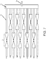
- electronic signal interrogation is to perform sequential integration by shorting one side of all lead wires and taking turns with left side electrical lead wires one at a time, e.g., every millisecond, such as in the configuration shown in FIG. 7 .
- 71 is an exemplary electrode pair for label-free detection of nucleotide attachment or detachment, (wherein the electrode pair would further include a biomolecule bridging the gap and probe molecule)
- 72 is an embodiment of a lead wire, such as an Au lead wire, which can be surface insulated or coated to prevent protein or other biomolecule adhesion thereon.
- element 73 is a common connection lead wire connecting all of the right side electrodes
- element 74 is just the one common lead wire needed on the right side of the array.
- the left side electrodes, Y1, Y2... Y10, are interrogated one at a time, sequentially. This wiring configuration and sequential interrogation method results in fewer electronic measurement complications compared to the handling of many thousands of parallel signals all at once.
- FIG. 7 type nano-tip or nano-pillar structure is stacked in three dimensions, such as shown in FIG. 8 , with an accompanying microfluidic chamber for each stack (top left in the figure), or with one or more common microfluidic chambers (top right in the figure).
- FIG. 8 In such 3D configurations, at least about one million to about one billion devices can be operated simultaneously for extremely rapid DNA or genome sequencing.
- a more sophisticated, micro-wire or micro-ribbon array with protruding Au pillar arrays are used for even higher density biomolecule sensing.
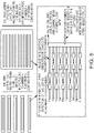
- FIG. 9 Aspects of the genome or DNA sequencing systems and methods are summarized in FIG. 9 .
- Appropriate software and a computer system are incorporated, and a microfluidic system is connected to the massively parallel electronic detection system.
- Biomolecules and coupling agents are delivered into the microfluidic chamber(s), together with nucleotides to be sequenced.
- FIG. 10 illustrates a molecular structure used for DNA sequence analysis, comprising a bridge and probe molecule structure.
- the bridge biomolecule comprises a synthetic double stranded DNA oligo molecule, 20 nm in length (60 bases), with thiol groups at both 5' ends of the molecule for coupling to the Au contact points provided on the metal electrodes.
- one bridge biomolecule bridges the ⁇ 10 nm nano-gap between the electrodes in each electrode pair.
- the Au contact points of each electrode pair may comprise any of the Au structures discussed herein above, such as, for example, Au dots electrodeposited on sharp ends of the electrodes or Au pillars grown by electrodeposition of Au into unmasked areas near the tips of the electrodes, and so forth.
- the metal electrodes may comprise platinum (Pt), palladium (Pd), rhodium (Rh) or gold (Au).
- the contact points and the electrodes comprise an integration of the same metal, i.e. Au.
- the probe molecule comprises a polymerase, for example, E. coli Pol I, which is chemically crosslinked to a streptavidin protein, which in turn is coupled to the bridge molecule at a biotinylated nucleotide provided within the synthetic DNA oligo sequence.
- the figure is shown to scale in regard to the sizes of the molecules and atoms.
- FIG. 11 illustrates an exemplary test set-up usable for electrical measurements on molecular sensors. Illustrated at top is a cross-sectional depiction of an electrode-substrate structure, and attachment to an analyzer for applying voltages and measuring currents through the bridge molecule. The structure at bottom is a perspective view of an electrode array for bridging circuits. Each pair of electrodes is illustrated as comprising Metal-2 contact points on Metal-1 electrodes. As discussed above, the Metal-1 electrodes may comprise Pt, Pd, Rh, or Au, and the Metal-2 contacts points comprise Au. Metal-1 and Metal-2 are both Au, such as when Au pillars are grown on unmasked areas of Au electrodes. In the present example, the Au tips or pillars support self-assembly of thiolated molecules in place by capitalizing on the strong thiol-Au binding.
- FIGS. 12(a)-(c) set forth electron micrographs of successfully constructed electrode pairs comprising Au contact points.
- FIG. 12(a) is an electron microscope image of Ti electrodes comprising Au dot contacts for bridge molecule binding. In this example, the Au dots were electrodeposited at or near the ends of the Ti electrodes. Electrodes are disposed on a silicon substrate, produced via e-beam lithography.
- FIG. 12(b) is an electron micrograph at higher resolution. The image is a close-up of the array in FIG. 12(a) , showing an electrode gap of 7 nm with Au dot contacts having 15 nm Au-to-Au spacing.
- FIG. 12(c) is an electron micrograph at even higher resolution. The image is a close-up of the array in FIG. 12(b) , showing approximately 10 nm Au dots deposited at the tips of the electrodes.
- the process of molecular sensor self-assembly onto gold-dot contact electrodes is shown being electronically monitored.
- Current versus time measurements are used to monitor self-assembly of the bridge and molecular sensor complex.
- the plot at the upper left shows Phase 1 of the self-assembly, wherein a double stranded DNA bridge with thiol groups on the 5' ends assembles onto electrode gold contact point, as evidenced by a jump in current.
- the plot at the upper right shows Phase 2 of the self-assembly process, wherein polymerase-streptavidin complex binds to a biotinylated site on the dsDNA bridge, as evidenced by another jump up in current.
- the plot at the lower left shows Phase 3 of the self-assembly process, wherein a primed single-stranded DNA template binds to the polymerase to complete the complex, as evidenced by another spike in current versus time.
- FIG. 14 provides electron microscope imaging of the final self-assembled structure upon completion of the self-assembly phases depicted and monitored in FIG. 13 and discussed herein.
- the bridge-complex is directly visible without labeling, and can be seen as a slightly blurry higher contrast region joining the electrode pair (and indicated by the white arrow in the higher magnification image at the right).
- the narrower portions of the two electrodes in the pair have a width of about 20 nm and a nanogap between the electrodes of about 7 nm.
- the image at left focuses on one pair of electrodes out of an array of pairs of electrodes.
- the whitish portions at the tips of each electrode are the gold (Au) islands, onto which the biomolecule is bound.
- Au gold
- the biomolecule (the whitish higher contrast blur between electrode tips) is seen as contiguous from one tip to the other across the nanogap.
- the plots in FIG. 15 show the current signals resulting from the sensor being supplied with various primed, single stranded DNA sequencing templates and dNTPs for incorporation and polymerization.
- the major signal spikes represent signals resulting from discrete incorporation events, wherein the polymerase enzyme adds another base to the extending strand.
- the template is 20 T bases.
- the template is 20 G bases.
- the template is 20 A bases.
- the template is 20 C bases.
- the approximate rate of incorporation observed is about 10 to 20 bases per second, which is consistent with standard enzyme kinetics except for the lower rate of ⁇ 1 base per second presumed due to rate limiting factors (e.g., lower dNTP concentration).
- Electrode pairs are provided that show two separate fabricated electrode pairs, each comprising Au-dot island contact points.
- the illustration above the micrographs diagrammatically shows how these electrodes and contact points would look like in a side view.
- these electrode pairs which are usable for DNA sequencing, have a 5-20 nm nano-gap and a pair of Au islands at the ends of the electrodes for attaching or immobilizing biomolecules, such as proteins or fragmented DNA, which will be bridged one molecule over each nano-gap.
- Devices comprising electrode pairs with bridging biomolecules are useful in the fluorescence-free (label-free) detection of DNA sequencing via electrical measurements.
- FIG. 17 sets forth two embodied electrode pair structures (a) and (b).
- the illustration at the top of each embodiment is a diagrammatic representation of the electrode structure, and the electron micrograph below shows the successful embodiment.
- Both (a) and (b) images are top views of nano-electrode geometries with different shapes, each produced by nano-imprint lithography for scaled-up manufacturing or e-beam lithography.
- sharp-tip electrodes comprising a pointed end were deposited with Au islands using electrodeposition.
- the sharp-tip electrodes are provided with a curvature culminating into narrow portions of the electrode where the Au is preferentially deposited.
- the Au islands were also electrodeposited.
- a passivation layer is exemplified.
- Au deposition may occur at sites on the electrodes other than at or near the electrode tips and these errant deposits would be capable of entering into unwanted binding with biomolecules.
- these inadvertent Au deposits can be covered up with passivation such that only the critical regions, i.e. the tips, of the electrodes remain exposed and available to participate self-assembly binding with biomolecules.
- FIG. 18 an illustration is provided to show diagrammatically where the passivation layers are located in relation to the electrode pair. The electron micrograph shows the passivation layer successfully in place over the electrode pair.
- the passivation layer shown in the micrograph added in this case by e-beam lithography patterning, prevents unwanted biomolecule attachment to any other Au present as errant deposits on the electrode surface.
- a passivation layer protects the electrodes from chemical exposure to solutions and prevents unwanted leakage current flowing through various solutions.
- the passivation layer embodied here is SiO 2 , although a variety of other insulating materials compatible with lithographic methods could be used, such as polymer resists (e.g., PMMA, SU8, etc.), or semiconductor-based materials such as silicon nitride.
- other nano-lithography patterning can be used to add a passivation layer over the electrodes besides e-beam lithography.
- FIG. 19 sets forth an electron micrograph demonstrating fabricated multi-Au-bead electrodes.
- a thin gold film was deposited on Ti electrodes and then the deposited film annealed.
- the results, as evidenced in the micrograph, are rows of uniformly sized and spaced Au beads arrayed along the centerline of the electrodes.
- FIG. 20 provides an electron micrograph demonstrating another fabricated multi-gold-bead electrodes. This illustrates the result of annealing a thin Au film deposited on an underlying Ti electrode, which produces rows of uniformly sized and spaced Au beads arrayed along the centerline of the electrodes.
- FIG. 21 provides an electron micrograph demonstrating successful addition of a passivation layer for use in sensing applications, which leaves open only a region near the tips of the electrodes. In this way, only a pair (or at most a few) of Au beads are left exposed as contact points for targeted molecular bridge binding.
- the passivation layer is SiO 2 , leaving open a 100 nm wide region near the tips (indicated by the dashed circle region).
- the surface of a Au island can be made to be as fresh as possible, such as to ensure easier and thus more likely adhesion/attachment of a biomolecule to an Au island, and to ensure a reliable and robust molecular electronic bridge for genome sequencing.
- An Au surface may become contaminated with trace amounts of organic or inorganic contaminants.
- An example of such a contaminant is a carbonaceous coating, occurring when an electrode with Au islands has been left in air or in contact with an aqueous solution or solvent for an extended period of time.
- FIG. 22 illustrates a flow-chart showing these four different approaches, and where these methods fit in a timing sequence to other steps used to make a label-free sequencing analysis device. As illustrated in the flow diagram, any one or more of these four methods are performed after the Au island formation on the electrode substrates. That is, Au islands would be first deposited onto nano-electrodes, (e.g. Pt, Pd, Rh, Ti, or Au).
- nano-electrodes e.g. Pt, Pd, Rh, Ti, or Au.
- any one or more of these four processes can also be used on Au nano-electrodes to freshen the surface of the Au nano-electrodes prior to deposition of Au islands. Thereafter, the Au islands deposited on Au nano-electrodes may have developed a contamination, and one or more of the four processes can be repeated again, this time to refresh the surfaces of the Au islands.
- the nano-electrode array is encased in a microfluidic environment and subjected to a biomolecule supply, such as an aqueous solution.
- the devices can be used for label-free sequencing analysis by use of the molecular bridges across each nano-electrode pair.
- the Au island pairs are subjected to sputter etching or ion etching.
- the amount of Au removed should be minimal so that the removed Au atoms do not end up deposited onto nearby areas whereupon biomolecules may inadvertently attach.
- the amount of Au to be removed may comprise the equivalent to at most 10 atomic layers of Au on average, or may comprise the equivalent to at most 5 atomic layers of Au, or may comprise the equivalent to at most an average 2 atomic layers of Au.
- a very thin layer of new Au atoms can be added onto the surface of the existing Au islands.
- Sputter deposition, evaporation, electroless deposition, electroplating, or ion implantation can be performed to add a fresh amount of Au.
- the amount of newly added Au should be minimal so as not to deposit Au on nearby areas, which may induce unwanted bonding of biomolecules to these nearby regions.
- the amount of Au to be added by these or other methods may be equivalent to at most 5 atomic layers of Au on average, or may be equivalent to at most 3 atomic layers of Au, or at most 1 atomic layer of Au.
- a device structure comprising a pair of Au islands for molecular bridge formation can be subjected to a thermal annealing process, such as by exposing the Au island containing device to a temperature of from about 100° to about 500° C, and preferably from about 200° to about 400° C, for a total time period of from about 0.01 to about 10,000 minutes in air, nitrogen, or argon, or in any other inert atmosphere.
- a thermal annealing process such as by exposing the Au island containing device to a temperature of from about 100° to about 500° C, and preferably from about 200° to about 400° C, for a total time period of from about 0.01 to about 10,000 minutes in air, nitrogen, or argon, or in any other inert atmosphere.
- a high intensity yet broadened areal beam of infrared (IR) or laser light can be radiated onto a device surface, such as in a pulse mode heating (e.g., more frequent than 10 pulses per minute) so that the heat propagation to the electronic device regions underneath is minimized.
- IR infrared
- pulse mode heating e.g., more frequent than 10 pulses per minute
- a highly focused laser beam or infrared light beam can be employed so as to locally heat up the regions near the Au islands, e.g., with a beam diameter less that 100 ⁇ m, preferably less than 2 ⁇ m, and even more preferably less than 0.1 ⁇ m. This can be accomplished by use of a beam focusing wave guide.
- Selective heating of metallic islands such as Au can be enabled using microwave heating, such as by using repeating pulse mode heating/cool-down cycles.
- microwave heating such as by using repeating pulse mode heating/cool-down cycles.
- a radio frequency (RF) radiation e.g., at 5 KHz to 500 KHz frequency, can be utilized, as this RF frequency range tends to preferentially and selectively heat up only conductive components.
- RF radio frequency
- RF radio frequency
- the activity of a Au surface can be enhanced if sulfur atoms are intentionally added.
- Such modification of Au surfaces with added sulfur atoms can be accomplished in a precisely controlled manner if the sulfur atoms are ion implanted, e.g., at an accelerating voltage of e.g., from about 5 to about 200 KV, and with a dose of about 10 5 to 10 16 ions/cm 2 . Implanted ions are lodged into the metal surface where they remain mechanically robust.
- adhesion layer material is a chromium (Cr) film on the substrate surface (e.g., SiO 2 ), rather than a titanium (Ti), zirconium (Zr), or tantalum (Ta) film, the formation and binding performance of Au islands is improved.
- Cr chromium
Landscapes
- Chemical & Material Sciences (AREA)
- Life Sciences & Earth Sciences (AREA)
- Health & Medical Sciences (AREA)
- Engineering & Computer Science (AREA)
- Physics & Mathematics (AREA)
- Molecular Biology (AREA)
- Biomedical Technology (AREA)
- Analytical Chemistry (AREA)
- Immunology (AREA)
- General Health & Medical Sciences (AREA)
- Biochemistry (AREA)
- Proteomics, Peptides & Aminoacids (AREA)
- Organic Chemistry (AREA)
- Electrochemistry (AREA)
- Chemical Kinetics & Catalysis (AREA)
- Spectroscopy & Molecular Physics (AREA)
- General Physics & Mathematics (AREA)
- Pathology (AREA)
- Biophysics (AREA)
- Nanotechnology (AREA)
- Wood Science & Technology (AREA)
- Zoology (AREA)
- General Chemical & Material Sciences (AREA)
- Hematology (AREA)
- Urology & Nephrology (AREA)
- Food Science & Technology (AREA)
- Medicinal Chemistry (AREA)
- General Engineering & Computer Science (AREA)
- Genetics & Genomics (AREA)
- Bioinformatics & Cheminformatics (AREA)
- Microbiology (AREA)
- Biotechnology (AREA)
- Materials Engineering (AREA)
- Apparatus Associated With Microorganisms And Enzymes (AREA)
- Measuring Or Testing Involving Enzymes Or Micro-Organisms (AREA)
- Investigating Or Analyzing Materials By The Use Of Electric Means (AREA)
Claims (10)
- DNA- oder Genom-Sequenzierungsstruktur, umfassend:(a) ein Elektrodenpaar (71), wobei jede Elektrode ein spitzenförmiges Ende aufweist, wobei die Elektroden durch einen Nanospalt getrennt sind, der durch die einander zugewandten spitzenförmigen Enden definiert ist,(b) mindestens eine leitende Insel, die an oder nahe bei jedem spitzenförmigen Ende jeder Elektrode abgeschieden ist, und(c) ein Biomolekül mit zwei Enden, wobei jedes der Enden an der mindestens einen leitenden Insel auf jeder der Elektroden befestigt ist, so dass ein Biomolekül den Nanospalt überbrückt,- wobei Wechselwirkungen des Nukleotids mit dem Biomolekül eine elektronische Überwachung der DNA- oder Genomsequenzierung ohne die Verwendung eines fluoreszierenden Elements ermöglichen,- dadurch gekennzeichnet, dass die Struktur eine Vielzahl von Schichten von Elektrodenpaaren umfasst, die eine dreidimensionale Anordnung bilden, wobei die Elektrodenpaare so miteinander verbunden sind, dass die einen Elektroden eines jeden Paars durch einen gemeinsamen Leitungsdraht (73) miteinander verbunden sind und jede der anderen Elektroden in jedem Paar nicht mit den anderen verbunden ist, was eine unabhängige und sequentielle Abfrage jedes Elektrodenpaares ermöglicht.
- Struktur nach Anspruch 1, wobei das Elektrodenpaar Platin (Pt), Palladium (Pd), Rhodium (Rh), Gold (Au) oder Titan (Ti) umfasst.
- Struktur nach Anspruch 1, wobei die mindestens eine leitende Insel Gold (Au) umfasst.
- Struktur nach Anspruch 3, wobei die mindestens eine leitende Insel Nanospitzen auf Gold(Au)-Basis umfasst, die durch galvanische Abscheidung von Gold (Au) an oder nahe eines jeden spitzenförmigen Endes jeder Elektrode erhalten werden, wobei die mindestens eine leitende Insel vorzugsweise Nanospitzen auf Gold(Au)-Basis umfasst, die durch galvanische Abscheidung von Gold (Au) an oder nahe eines jeden spitzenförmigen Endes jeder Elektrode und anschließendes Tempern nach der galvanischen Abscheidung erhalten werden.
- Struktur nach Anspruch 3, wobei die mindestens eine leitende Insel die Form einer Säule hat, wobei die Säule auf jeder Elektrode durch einen galvanischen Abscheidungsprozess gezüchtet wird,- wobei die Säule optional einen Durchmesser von weniger als 20 nm und eine Höhe von weniger als 25 nm hat oder die Säule einen Durchmesser von weniger als 7 nm und eine Höhe von weniger als 10 nm hat.
- Struktur nach Anspruch 1, wobei die mindestens eine leitfähige Insel galvanisch oder stromlos abgeschiedenes Metall umfasst, um eine nanospitzenförmige oder nanosäulenförmige leitfähige Insel mit einer freiliegenden Abmessung von weniger als 20 nm zu bilden, wobei die Nanospitze oder Nanosäule vorzugsweise eine verzweigte oder poröse Oberfläche mit einer Porosität von mindestens 30 % umfasst, um den Oberflächenbereich der freiliegenden Oberfläche der Nanospitze oder Nanosäule um mindestens 10 % im Vergleich zu der Nanospitzen- oder Nanosäulenstruktur nach der galvanischen oder stromlosen Abscheidung auf jeder Elektrode zu vergrößern.
- Struktur nach Anspruch 1, wobei die Kontaktfläche zwischen der mindestens einen leitfähigen Insel und der Elektrode, auf der sie abgeschieden ist, mindestens 50% des Durchmessers der leitfähigen Insel beträgt.
- Struktur nach Anspruch 1, wobei jedes Ende des Biomoleküls durch Antikörper-Antigen-Bindung oder Streptavidin-Biotin-Bindung an die mindestens eine leitende Insel gebunden ist.
- Struktur nach Anspruch 3, wobei jedes Ende des Biomoleküls an die mindestens eine leitende Insel durch Thiol-Gold(Au)-Bindung oder goldbindende Proteine gebunden ist.
- Genom- oder DNA-Sequenzierungssystem, umfassend:(a) die DNA- oder Genomsequenzierungsstruktur nach Anspruch 1, und(b) eine Kammer, welche die Struktur umschließt und ein mikrofluidisches Subsystem definiert, das zur Zufuhr von Biomolekülen, Nukleotiden, PBS oder Wasserlösungen zu dem Elektrodenpaar verwendet werden kann.
Priority Applications (1)
| Application Number | Priority Date | Filing Date | Title |
|---|---|---|---|
| EP22186552.0A EP4137808A1 (de) | 2016-01-28 | 2017-01-27 | Verfahren zur herstellung einer dna-sequenzierungsvorrichtung |
Applications Claiming Priority (2)
| Application Number | Priority Date | Filing Date | Title |
|---|---|---|---|
| US201662288364P | 2016-01-28 | 2016-01-28 | |
| PCT/US2017/015437 WO2017132567A1 (en) | 2016-01-28 | 2017-01-27 | Massively parallel dna sequencing apparatus |
Related Child Applications (1)
| Application Number | Title | Priority Date | Filing Date |
|---|---|---|---|
| EP22186552.0A Division EP4137808A1 (de) | 2016-01-28 | 2017-01-27 | Verfahren zur herstellung einer dna-sequenzierungsvorrichtung |
Publications (3)
| Publication Number | Publication Date |
|---|---|
| EP3408219A1 EP3408219A1 (de) | 2018-12-05 |
| EP3408219A4 EP3408219A4 (de) | 2020-02-26 |
| EP3408219B1 true EP3408219B1 (de) | 2022-08-17 |
Family
ID=59398944
Family Applications (2)
| Application Number | Title | Priority Date | Filing Date |
|---|---|---|---|
| EP17745013.7A Active EP3408219B1 (de) | 2016-01-28 | 2017-01-27 | Massiv parallele dna-sequenzierungsvorrichtung |
| EP22186552.0A Withdrawn EP4137808A1 (de) | 2016-01-28 | 2017-01-27 | Verfahren zur herstellung einer dna-sequenzierungsvorrichtung |
Family Applications After (1)
| Application Number | Title | Priority Date | Filing Date |
|---|---|---|---|
| EP22186552.0A Withdrawn EP4137808A1 (de) | 2016-01-28 | 2017-01-27 | Verfahren zur herstellung einer dna-sequenzierungsvorrichtung |
Country Status (6)
| Country | Link |
|---|---|
| US (2) | US10712334B2 (de) |
| EP (2) | EP3408219B1 (de) |
| JP (1) | JP7080489B2 (de) |
| KR (2) | KR102763291B1 (de) |
| CN (1) | CN109328301B (de) |
| WO (1) | WO2017132567A1 (de) |
Families Citing this family (43)
| Publication number | Priority date | Publication date | Assignee | Title |
|---|---|---|---|---|
| CA3021580A1 (en) | 2015-06-25 | 2016-12-29 | Barry L. Merriman | Biomolecular sensors and methods |
| CN113985017A (zh) | 2016-01-14 | 2022-01-28 | 罗斯韦尔生物技术股份有限公司 | 分子传感器及相关方法 |
| EP3408219B1 (de) | 2016-01-28 | 2022-08-17 | Roswell Biotechnologies, Inc | Massiv parallele dna-sequenzierungsvorrichtung |
| JP7280590B2 (ja) | 2016-01-28 | 2023-05-24 | ロズウェル バイオテクノロジーズ,インコーポレイテッド | 大スケールの分子電子工学センサアレイを使用する被分析物を測定するための方法および装置 |
| KR20240170584A (ko) | 2016-02-09 | 2024-12-03 | 로스웰 엠이 아이엔씨. | 전자 비표지 dna 및 게놈 시퀀싱 |
| US10597767B2 (en) | 2016-02-22 | 2020-03-24 | Roswell Biotechnologies, Inc. | Nanoparticle fabrication |
| US11514289B1 (en) | 2016-03-09 | 2022-11-29 | Freenome Holdings, Inc. | Generating machine learning models using genetic data |
| US9829456B1 (en) | 2016-07-26 | 2017-11-28 | Roswell Biotechnologies, Inc. | Method of making a multi-electrode structure usable in molecular sensing devices |
| KR102622275B1 (ko) | 2017-01-10 | 2024-01-05 | 로스웰 바이오테크놀로지스 인코포레이티드 | Dna 데이터 저장을 위한 방법들 및 시스템들 |
| CA3052140A1 (en) | 2017-01-19 | 2018-07-26 | Roswell Biotechnologies, Inc. | Solid state sequencing devices comprising two dimensional layer materials |
| US10641726B2 (en) * | 2017-02-01 | 2020-05-05 | Seagate Technology Llc | Fabrication of a nanochannel for DNA sequencing using electrical plating to achieve tunneling electrode gap |
| US10731210B2 (en) | 2017-02-01 | 2020-08-04 | Seagate Technology Llc | Fabrication of nanochannel with integrated electrodes for DNA sequencing using tunneling current |
| US10857575B2 (en) | 2017-02-27 | 2020-12-08 | Nanovation Partners LLC | Shelf-life-improved nanostructured implant systems and methods |
| US20180259475A1 (en) | 2017-03-09 | 2018-09-13 | Seagate Technology Llc | Vertical nanopore coupled with a pair of transverse electrodes having a uniform ultrasmall nanogap for dna sequencing |
| US10508296B2 (en) | 2017-04-25 | 2019-12-17 | Roswell Biotechnologies, Inc. | Enzymatic circuits for molecular sensors |
| EP3615685B1 (de) | 2017-04-25 | 2025-02-19 | Roswell Biotechnologies, Inc | Enzymatische schaltungen für molekulare sensoren |
| EP4023764A3 (de) | 2017-05-09 | 2022-09-21 | Roswell Biotechnologies, Inc. | Bindungssondenschaltungen für molekulare sensoren |
| CN111373049A (zh) | 2017-08-30 | 2020-07-03 | 罗斯威尔生命技术公司 | 用于dna数据存储的进行性酶分子电子传感器 |
| CN111373051A (zh) | 2017-10-10 | 2020-07-03 | 罗斯威尔生命技术公司 | 用于无扩增dna数据存储的方法、装置和系统 |
| TWI772618B (zh) * | 2018-03-02 | 2022-08-01 | 國立研究開發法人科學技術振興機構 | 奈米縫隙電極及其製作方法以及具有奈米縫隙電極的奈米裝置 |
| TWI815865B (zh) | 2018-03-02 | 2023-09-21 | 國立研究開發法人科學技術振興機構 | 單分子電晶體 |
| EP3791179A4 (de) | 2018-05-09 | 2022-01-26 | Arizona Board of Regents on behalf of Arizona State University | Verfahren zur elektronischen detektion und quantifizierung von antikörpern |
| IL278769B2 (en) | 2018-05-17 | 2025-06-01 | Stuart Lindsay | Device, system and method for direct electrical measurement of enzyme activity |
| US11621345B2 (en) * | 2018-08-14 | 2023-04-04 | Pawan Tyagi | Systems and methods of fabricating gate electrode on trenched bottom electrode based molecular spintronics device |
| WO2020071025A1 (ja) * | 2018-10-02 | 2020-04-09 | 国立研究開発法人科学技術振興機構 | ヘテロエピタキシャル構造体及びその作製方法、並びにヘテロエピタキシャル構造を含む金属積層体及びその作製方法、ナノギャップ電極及びナノギャップ電極の作製方法 |
| AU2020214334A1 (en) | 2019-01-30 | 2021-08-12 | Arizona Board Of Regents On Behalf Of Arizona State University | Bioelectronic circuits, systems and methods for preparing and using them |
| WO2020198530A1 (en) * | 2019-03-26 | 2020-10-01 | Roswell Biotechnologies, Inc. | Tunable nanopillar and nanogap electrode structures and methods thereof |
| CN113994013A (zh) | 2019-04-12 | 2022-01-28 | 罗斯威尔生命技术公司 | 用于分子电子学传感器的多环芳族桥 |
| US12146852B2 (en) | 2019-09-06 | 2024-11-19 | Roswell Biotechnologies, Inc. | Methods of fabricating nanoscale structures usable in molecular sensors and other devices |
| JP7237388B2 (ja) * | 2019-12-03 | 2023-03-13 | 国立研究開発法人科学技術振興機構 | ナノポア構造体、ナノポア構造体を含む塩基配列解析装置 |
| JP2023513083A (ja) * | 2020-01-31 | 2023-03-30 | ユニバーサル シーケンシング テクノロジー コーポレイション | ナノ電子工学測定のために作出された高分子 |
| KR20230002461A (ko) * | 2020-03-25 | 2023-01-05 | 유니버셜 시퀀싱 테크놀로지 코퍼레이션 | 나노갭 디바이스에 직접 부착된 효소 돌연변이체 |
| CN115552030A (zh) | 2020-04-17 | 2022-12-30 | 代表亚利桑那大学的亚利桑那校董事会 | 单分子电子序列检测器及其使用方法 |
| AU2021263432A1 (en) * | 2020-04-30 | 2022-12-01 | Arizona Board Of Regents On Behalf Of Arizona State University | Methods for sequencing biopolymers |
| WO2021226291A1 (en) * | 2020-05-05 | 2021-11-11 | Roswell Biotechnologies, Inc. | Single-biomolecule-bridged sequencing biosensors and storage devices and methods for same |
| EP4150116A2 (de) | 2020-05-11 | 2023-03-22 | Illumina, Inc. | Vorrichtungen mit an elektroden gekoppelten partikeln und verfahren zur herstellung und verwendung davon |
| US12276653B2 (en) | 2020-05-29 | 2025-04-15 | Arizona Board Of Regents On Behalf Of Arizona State University | Bioelectronic devices with programmable adaptors |
| US20220252542A1 (en) * | 2020-09-02 | 2022-08-11 | Roswell Biotechnologies, Inc. | Single molecule nanoparticle nanowire for molecular electronic sensing |
| JP2023540499A (ja) * | 2020-09-02 | 2023-09-25 | ロズウェル バイオテクノロジーズ,インコーポレイテッド | 分子電子センシングのための単一分子ナノ粒子ナノワイヤ |
| JP2024512838A (ja) | 2021-03-31 | 2024-03-21 | イルミナ インコーポレイテッド | 分子検出のためのスケーラブル回路 |
| US12624389B2 (en) | 2021-06-07 | 2026-05-12 | Arizona Board Of Regents On Behalf Of Arizona State University | Methods for sequencing biopolymers |
| US12163979B2 (en) * | 2021-11-08 | 2024-12-10 | Versitech Limited | Nano robotic system for high throughput single cell DNA sequencing |
| KR20260026475A (ko) * | 2023-04-15 | 2026-02-26 | 세미콘바이오 아이엔씨. | 금속-비금속 화합물 반도체 나노브릿지 어레이를 갖는 전자 바이오 센서 |
Family Cites Families (294)
| Publication number | Priority date | Publication date | Assignee | Title |
|---|---|---|---|---|
| JPS5938647A (ja) * | 1982-08-28 | 1984-03-02 | Toshiba Corp | イオン選択性電極装置と流通型イオン分析装置 |
| US4923586A (en) | 1987-03-31 | 1990-05-08 | Daikin Industries, Ltd. | Enzyme electrode unit |
| US5082627A (en) | 1987-05-01 | 1992-01-21 | Biotronic Systems Corporation | Three dimensional binding site array for interfering with an electrical field |
| JPH0233981A (ja) | 1988-07-23 | 1990-02-05 | Nec Corp | 多素子センサ |
| US5486449A (en) | 1989-02-07 | 1996-01-23 | Rohm Co., Ltd. | Photomask, photoresist and photolithography for a monolithic IC |
| GB2244135B (en) | 1990-05-04 | 1994-07-13 | Gen Electric Co Plc | Sensor devices |
| US5282844A (en) * | 1990-06-15 | 1994-02-01 | Medtronic, Inc. | High impedance, low polarization, low threshold miniature steriod eluting pacing lead electrodes |
| US6051380A (en) | 1993-11-01 | 2000-04-18 | Nanogen, Inc. | Methods and procedures for molecular biological analysis and diagnostics |
| IL103674A0 (en) | 1991-11-19 | 1993-04-04 | Houston Advanced Res Center | Method and apparatus for molecule detection |
| US5414588A (en) | 1993-09-20 | 1995-05-09 | The Regents Of The University Of California | High performance capacitors using nano-structure multilayer materials fabrication |
| US5366140A (en) | 1993-09-30 | 1994-11-22 | Minnesota Mining And Manufacturing Company | Patterned array of uniform metal microbeads |
| US5965452A (en) | 1996-07-09 | 1999-10-12 | Nanogen, Inc. | Multiplexed active biologic array |
| US5871918A (en) | 1996-06-20 | 1999-02-16 | The University Of North Carolina At Chapel Hill | Electrochemical detection of nucleic acid hybridization |
| JP3149718B2 (ja) | 1995-02-03 | 2001-03-26 | 松下電器産業株式会社 | 単電子トランジスタ |
| US5583359A (en) | 1995-03-03 | 1996-12-10 | Northern Telecom Limited | Capacitor structure for an integrated circuit |
| US6673533B1 (en) | 1995-03-10 | 2004-01-06 | Meso Scale Technologies, Llc. | Multi-array multi-specific electrochemiluminescence testing |
| US5639507A (en) | 1995-05-03 | 1997-06-17 | Avx Corporation | Method of making a planar multi-layer capacitor |
| DE69632921T2 (de) | 1995-12-01 | 2005-07-14 | Innogenetics N.V. | System und verfahren zur bestimmung der impedanz und herstellungsverfahren |
| US6033582A (en) | 1996-01-22 | 2000-03-07 | Etex Corporation | Surface modification of medical implants |
| US5881184A (en) | 1996-05-22 | 1999-03-09 | Eastman Kodak Company | Active pixel sensor with single pixel reset |
| US6506564B1 (en) | 1996-07-29 | 2003-01-14 | Nanosphere, Inc. | Nanoparticles having oligonucleotides attached thereto and uses therefor |
| US6202471B1 (en) | 1997-10-10 | 2001-03-20 | Nanomaterials Research Corporation | Low-cost multilaminate sensors |
| US6110354A (en) | 1996-11-01 | 2000-08-29 | University Of Washington | Microband electrode arrays |
| US5767687A (en) | 1996-11-29 | 1998-06-16 | Geist; Jon | Surface-capacitor type condensable-vapor sensor |
| US6706473B1 (en) | 1996-12-06 | 2004-03-16 | Nanogen, Inc. | Systems and devices for photoelectrophoretic transport and hybridization of oligonucleotides |
| US7169272B2 (en) | 1997-04-30 | 2007-01-30 | Board Of Trustees Of The University Of Arkansas | Microfabricated recessed disk microelectrodes: characterization in static and convective solutions |
| US5982018A (en) | 1997-05-23 | 1999-11-09 | Micron Technology, Inc. | Thin film capacitor coupons for memory modules and multi-chip modules |
| FR2764386B1 (fr) | 1997-06-06 | 1999-07-16 | Commissariat Energie Atomique | Support d'electrodes comportant au moins une electrode recouverte par un depot et systeme de lecture de ce support |
| JP2000033712A (ja) | 1997-09-30 | 2000-02-02 | Seiko Epson Corp | マイクロセンサーデバイス作成方法及びそれを用いた液体機能評価方法 |
| US6123819A (en) | 1997-11-12 | 2000-09-26 | Protiveris, Inc. | Nanoelectrode arrays |
| US6537747B1 (en) | 1998-02-03 | 2003-03-25 | Lucent Technologies Inc. | Data transmission using DNA oligomers |
| US6060023A (en) | 1998-03-31 | 2000-05-09 | Motorola, Inc. | Molecular sensing apparatus |
| IL124322A (en) | 1998-05-04 | 2002-05-23 | Technion Res & Dev Foundation | Detection of an entity in a sample |
| AU767122B2 (en) | 1998-06-10 | 2003-10-30 | Georgia Tech Research Corporation | Microneedle devices and methods of manufacture and use thereof |
| US6238927B1 (en) | 1998-10-05 | 2001-05-29 | Mosaic Technologies, Incorporated | Reverse displacement assay for detection of nucleic acid sequences |
| US6094335A (en) | 1998-10-09 | 2000-07-25 | Advanced Micro Devices, Inc. | Vertical parallel plate capacitor |
| WO2000050232A1 (en) | 1999-02-25 | 2000-08-31 | Seiko Epson Corporation | Structure member excellent in water-repellency and manufacturing method thereof |
| US6517669B2 (en) | 1999-02-26 | 2003-02-11 | Micron Technology, Inc. | Apparatus and method of detecting endpoint of a dielectric etch |
| CA2367405A1 (en) | 1999-04-07 | 2000-10-12 | Dennis Michael Connolly | High resolution dna detection methods and devices |
| DE19916921A1 (de) | 1999-04-14 | 2000-10-19 | Fraunhofer Ges Forschung | Elektrisches Sensorarray |
| US7122152B2 (en) | 1999-05-10 | 2006-10-17 | University Of Florida | Spatiotemporal and geometric optimization of sensor arrays for detecting analytes fluids |
| AU7952700A (en) | 1999-10-20 | 2001-04-30 | Takatoshi Miyahara | Gene detecting chip, detector, and detecting method |
| DE19960076C2 (de) | 1999-12-13 | 2002-12-05 | November Ag Molekulare Medizin | Verfahren und Vorrichtung zum Nachweis und zur Quantifizierung von Biomolekülen |
| US20020090649A1 (en) | 1999-12-15 | 2002-07-11 | Tony Chan | High density column and row addressable electrode arrays |
| DE10015818A1 (de) | 2000-03-30 | 2001-10-18 | Infineon Technologies Ag | Biosensor und Verfahren zum Ermitteln makromolekularer Biopolymere mit einem Biosensor |
| WO2001079529A1 (en) | 2000-04-17 | 2001-10-25 | Purdue Research Foundation | Biosensor and related method |
| EP1278821A4 (de) * | 2000-05-03 | 2005-11-09 | Jen Gau Jr | Biologisches identifikationssystem mit integriertem sensorchip |
| FR2811316B1 (fr) | 2000-07-06 | 2003-01-10 | Saint Gobain | Substrat texture transparent et procedes pour l'obtenir |
| US6670131B2 (en) | 2000-11-30 | 2003-12-30 | Kabushiki Kaisha Toshiba | Nucleic acid detection method and apparatus, and vessel for detecting nucleic acid |
| NL1016779C2 (nl) | 2000-12-02 | 2002-06-04 | Cornelis Johannes Maria V Rijn | Matrijs, werkwijze voor het vervaardigen van precisieproducten met behulp van een matrijs, alsmede precisieproducten, in het bijzonder microzeven en membraanfilters, vervaardigd met een dergelijke matrijs. |
| DE10063739B4 (de) | 2000-12-21 | 2009-04-02 | Ferro Gmbh | Substrate mit selbstreinigender Oberfläche, Verfahren zu deren Herstellung und deren Verwendung |
| WO2002079514A1 (en) | 2001-01-10 | 2002-10-10 | The Trustees Of Boston College | Dna-bridged carbon nanotube arrays |
| US6749731B2 (en) | 2001-01-31 | 2004-06-15 | Kyocera Corporation | Gene detection chip and detection device |
| KR100878281B1 (ko) | 2001-03-14 | 2009-01-12 | 유니버시티 오브 매사츄세츠 | 나노 제조 |
| DE10113550A1 (de) | 2001-03-20 | 2002-10-02 | Infineon Technologies Ag | Verfahren zum Erfassen von makromolekularen Biopolymeren mittels einer Elektrodenanordnung |
| US6824974B2 (en) | 2001-06-11 | 2004-11-30 | Genorx, Inc. | Electronic detection of biological molecules using thin layers |
| US20040048241A1 (en) | 2001-06-11 | 2004-03-11 | Freeman Beverly Annette | Methods for attaching molecules |
| EP1417352A4 (de) | 2001-06-11 | 2006-11-08 | Genorx Inc | Elektronischer nachweis biologischer moleküle mittels dünnschichten |
| US20040023253A1 (en) | 2001-06-11 | 2004-02-05 | Sandeep Kunwar | Device structure for closely spaced electrodes |
| US7297494B2 (en) | 2001-06-25 | 2007-11-20 | Georgia Tech Research Corporation | Activatable probes and methods for in vivo gene detection |
| EP1425065A4 (de) | 2001-07-12 | 2004-12-15 | Merck & Co Inc | Elektrische feldstimulation mit eukaryontischen zellen |
| US6483125B1 (en) | 2001-07-13 | 2002-11-19 | North Carolina State University | Single electron transistors in which the thickness of an insulating layer defines spacing between electrodes |
| US20030040000A1 (en) | 2001-08-08 | 2003-02-27 | Connolly Dennis M. | Methods for attaching nucleic acid molecules to electrically conductive surfaces |
| US7052616B2 (en) | 2001-08-14 | 2006-05-30 | The Penn State Research Foundation | Fabrication of molecular scale devices using fluidic assembly |
| US6861224B2 (en) | 2001-11-02 | 2005-03-01 | Fujitsu Limited | Protein detecting device |
| JP2005508198A (ja) | 2001-11-06 | 2005-03-31 | インテグレイティド ナノ−テクノロジーズ エルエルシー | 試料中の生物物質を検出するためのシステム |
| US6905586B2 (en) * | 2002-01-28 | 2005-06-14 | Ut-Battelle, Llc | DNA and RNA sequencing by nanoscale reading through programmable electrophoresis and nanoelectrode-gated tunneling and dielectric detection |
| US6743368B2 (en) | 2002-01-31 | 2004-06-01 | Hewlett-Packard Development Company, L.P. | Nano-size imprinting stamp using spacer technique |
| WO2003091458A1 (en) | 2002-04-26 | 2003-11-06 | The Penn State Research Foundation | Integrated nanomechanical sensor array chips |
| EP1511862A4 (de) | 2002-05-14 | 2006-01-18 | Nanosphere Inc | Elektrischer nachweis von dna-hybridisierung und spezifischen bindungsereignissen |
| US20030224387A1 (en) | 2002-05-22 | 2003-12-04 | Sandeep Kunwar | Association of molecules with electrodes of an array of electrodes |
| EP1516377A2 (de) | 2002-06-05 | 2005-03-23 | Reveo, Inc. | Geschichtete elektrochemische zelle und verfahren zu deren herstellung |
| EP1376111A1 (de) | 2002-06-24 | 2004-01-02 | Universite Catholique De Louvain | Verfahren und Vorrichtung für die hochempfindliche Bestimmung von DNA und anderen Testsubstanzen |
| DE10397003B4 (de) | 2002-07-02 | 2015-04-30 | Panasonic Healthcare Holdings Co., Ltd. | Biosensor, Biosensorchip und Biosensoreinrichtung |
| US6755423B2 (en) | 2002-07-17 | 2004-06-29 | Li Jiun Chiu | Tool coupling device for changeable tool members |
| US7470533B2 (en) | 2002-12-20 | 2008-12-30 | Acea Biosciences | Impedance based devices and methods for use in assays |
| DE10242560A1 (de) | 2002-09-13 | 2004-03-25 | Creavis Gesellschaft Für Technologie Und Innovation Mbh | Herstellung von selbstreinigenden Oberflächen auf textilen Beschichtungen |
| US20040063100A1 (en) | 2002-09-30 | 2004-04-01 | Wang Chung Lin | Nanoneedle chips and the production thereof |
| DE10247679A1 (de) | 2002-10-12 | 2004-04-22 | Fujitsu Ltd., Kawasaki | Halbleitergrundstruktur für Molekularelektronik und Molekularelektronik-basierte Biosensorik |
| US7183055B2 (en) | 2002-11-01 | 2007-02-27 | Wisconsin Alumni Research Foundation | Direct radio-frequency detection of nucleotide hybridization at microelectrodes |
| JP2004191341A (ja) * | 2002-12-13 | 2004-07-08 | Canon Inc | 分子認識素子、これを用いたバイオセンサ、及びその製造方法 |
| WO2004065570A2 (en) | 2003-01-23 | 2004-08-05 | Integrated Nano-Technologies, Llc | Methods of metallizing nucleic acid molecules and methods of attaching nucleic acid molecules to conductive surfaces |
| AU2003304085A1 (en) | 2003-02-07 | 2004-11-26 | Wisconsin Alumni Research Foundation | Nanocylinder-modified surfaces |
| US20050164371A1 (en) | 2003-03-28 | 2005-07-28 | Fujitsu Limited | Cavity electrode structure, and sensor and protein detection device using the same |
| US7172917B2 (en) | 2003-04-17 | 2007-02-06 | Robert Bosch Gmbh | Method of making a nanogap for variable capacitive elements, and device having a nanogap |
| US7985475B2 (en) | 2003-04-28 | 2011-07-26 | Nanosys, Inc. | Super-hydrophobic surfaces, methods of their construction and uses therefor |
| WO2004096986A2 (en) | 2003-04-29 | 2004-11-11 | Integrated Nano-Technologies, Llc | Method for quantitative detection of nucleic acid molecules |
| JP2004347532A (ja) | 2003-05-23 | 2004-12-09 | Japan Science & Technology Agency | バイオセンサー |
| US20050156157A1 (en) | 2003-07-21 | 2005-07-21 | Parsons Gregory N. | Hierarchical assembly of interconnects for molecular electronics |
| JP4059181B2 (ja) | 2003-09-29 | 2008-03-12 | 株式会社村田製作所 | 多端子型積層セラミック電子部品の製造方法 |
| JP2005109269A (ja) | 2003-09-30 | 2005-04-21 | Hitachi Ltd | 半導体放射線検出器及び半導体放射線撮像装置 |
| US7132298B2 (en) | 2003-10-07 | 2006-11-07 | Hewlett-Packard Development Company, L.P. | Fabrication of nano-object array |
| EP1697495A2 (de) | 2003-11-20 | 2006-09-06 | Biowarn, Llc | Methodik und vorrichtung zum nachweis biologischer substanzen |
| WO2005108612A2 (en) | 2003-11-28 | 2005-11-17 | Genorx, Inc. | Nanoscale biosensor device, system and technique |
| WO2005059532A1 (en) | 2003-12-16 | 2005-06-30 | Dynabyte Informationssysteme Gmbh | Cartridge device for blood analysis |
| DE10359173B4 (de) | 2003-12-17 | 2006-11-09 | Robert Bosch Gmbh | Messvorrichtung mit mehreren auf einem Substrat angeordneten potentiometrischen Elektrodenpaaren |
| US7451381B2 (en) | 2004-02-03 | 2008-11-11 | Phonex Broadband Corporation | Reliable method and system for efficiently transporting dynamic data across a network |
| US20050247573A1 (en) | 2004-03-23 | 2005-11-10 | Hideaki Nakamura | Biosensors |
| US8354066B2 (en) | 2004-03-24 | 2013-01-15 | Technion Research & Development Foundation Ltd. | Artificial receptors |
| US20050221473A1 (en) | 2004-03-30 | 2005-10-06 | Intel Corporation | Sensor array integrated circuits |
| US8138496B2 (en) | 2004-04-01 | 2012-03-20 | Nanyang Technological University | Addressable transistor chip for conducting assays |
| US20060019273A1 (en) | 2004-05-12 | 2006-01-26 | Connolly Dennis M | Detection card for analyzing a sample for a target nucleic acid molecule, and uses thereof |
| US7385295B2 (en) | 2004-06-24 | 2008-06-10 | California Institute Of Technology | Fabrication of nano-gap electrode arrays by the construction and selective chemical etching of nano-crosswire stacks |
| US7265019B2 (en) | 2004-06-30 | 2007-09-04 | International Business Machines Corporation | Elastomeric CMOS based micro electromechanical varactor |
| US7150904B2 (en) | 2004-07-27 | 2006-12-19 | Ut-Battelle, Llc | Composite, ordered material having sharp surface features |
| US7258731B2 (en) | 2004-07-27 | 2007-08-21 | Ut Battelle, Llc | Composite, nanostructured, super-hydrophobic material |
| US7655275B2 (en) | 2004-08-02 | 2010-02-02 | Hewlett-Packard Delopment Company, L.P. | Methods of controlling flow |
| US20060029808A1 (en) | 2004-08-06 | 2006-02-09 | Lei Zhai | Superhydrophobic coatings |
| EP1630127B1 (de) | 2004-08-31 | 2008-09-10 | STMicroelectronics S.r.l. | Verfahren zur Herstellung einer Wirtsstruktur für nanometergroße Elemente |
| EP1630882B1 (de) | 2004-08-31 | 2012-05-02 | STMicroelectronics S.r.l. | Nanometrische Struktur und Verfahren zu ihrer Herstellung |
| DE102004042729B4 (de) | 2004-09-03 | 2018-02-01 | Robert Bosch Gmbh | Bio-Chip mit einem Elektrodenarray auf einem Substrat |
| US20070048748A1 (en) | 2004-09-24 | 2007-03-01 | Li-Cor, Inc. | Mutant polymerases for sequencing and genotyping |
| US7507320B2 (en) * | 2004-10-09 | 2009-03-24 | Academia Sinica | Single-atom tip and preparation method thereof |
| CN101006338A (zh) | 2004-10-14 | 2007-07-25 | 株式会社东芝 | 基于fet的核酸探测传感器 |
| US7541004B2 (en) | 2004-11-12 | 2009-06-02 | Predict, Inc. | MEMS-based sensor for lubricant analysis |
| US7785785B2 (en) | 2004-11-12 | 2010-08-31 | The Board Of Trustees Of The Leland Stanford Junior University | Charge perturbation detection system for DNA and other molecules |
| DE102004060738B4 (de) | 2004-12-15 | 2008-07-03 | Forschungszentrum Jülich GmbH | Verfahren zum strukturierten Aufbringen von Molekülen auf eine Leiterbahn |
| EP1848990A1 (de) | 2005-02-18 | 2007-10-31 | Midorion Ab | Sensor für den nachweis von einzelmolekülen |
| US9695472B2 (en) | 2005-03-04 | 2017-07-04 | Intel Corporation | Sensor arrays and nucleic acid sequencing applications |
| US8039368B2 (en) | 2005-03-21 | 2011-10-18 | The Trustees Of The University Of Pennsylvania | Nanogaps: methods and devices containing same |
| WO2006102905A1 (en) | 2005-03-31 | 2006-10-05 | Gregersen Enterprises 2005 Aps | Apparatus and method for a global model of hollow internal organs including the determination of cross-sectional areas and volume in internal hollow organs and wall properties |
| US7985451B2 (en) | 2005-04-01 | 2011-07-26 | Clemson University | Method of manufacturing ultrahydrophobic substrates |
| US7579184B2 (en) | 2005-06-02 | 2009-08-25 | Board Of Trustees Of Michigan State University | Methods to increase dynamic range and improve quantitative analysis in rapid biosensors |
| US7417418B1 (en) | 2005-06-14 | 2008-08-26 | Ayliffe Harold E | Thin film sensor |
| WO2007053242A2 (en) | 2005-09-19 | 2007-05-10 | Wayne State University | Transparent hydrophobic article having self-cleaning and liquid repellant features and method of fabricating same |
| FR2893266B1 (fr) | 2005-11-14 | 2007-12-21 | Commissariat Energie Atomique | Produit superhydrophile ou superhydrophobe, procede pour sa realisation et utilisation de ce produit |
| KR100757389B1 (ko) | 2005-12-06 | 2007-09-11 | 한국전자통신연구원 | 나노갭 전극을 갖는 센서 및 그 제조 방법 |
| WO2007133288A1 (en) | 2005-12-15 | 2007-11-22 | The Trustees Of Columbia University In The City Of New York | Sensing devices from molecular electronic devices utilizing hexabenzocoronenes |
| US8706219B2 (en) | 2005-12-22 | 2014-04-22 | Board Of Regents, The University Of Texas System | Method and apparatus for monitoring an organ of a patient |
| US7649198B2 (en) | 2005-12-28 | 2010-01-19 | Industrial Technology Research Institute | Nano-array and fabrication method thereof |
| US20070207487A1 (en) | 2006-01-25 | 2007-09-06 | Emig Christopher J | Photoelectrochemical synthesis of high density combinatorial polymer arrays |
| WO2007102960A2 (en) | 2006-01-30 | 2007-09-13 | Ashland Licensing And Intellectual Property Llc | Hydrophobic self-cleaning coating compositions |
| US20070184247A1 (en) | 2006-02-03 | 2007-08-09 | Simpson John T | Transparent, super-hydrophobic, disordered composite material |
| US7357018B2 (en) | 2006-02-10 | 2008-04-15 | Agilent Technologies, Inc. | Method for performing a measurement inside a specimen using an insertable nanoscale FET probe |
| EP2002248A1 (de) | 2006-03-17 | 2008-12-17 | Element Six Limited | Mikroelektroden-array |
| US20090011222A1 (en) | 2006-03-27 | 2009-01-08 | Georgia Tech Research Corporation | Superhydrophobic surface and method for forming same |
| US20070227300A1 (en) | 2006-03-31 | 2007-10-04 | Quantumsphere, Inc. | Compositions of nanometal particles containing a metal or alloy and platinum particles for use in fuel cells |
| US20070231542A1 (en) | 2006-04-03 | 2007-10-04 | General Electric Company | Articles having low wettability and high light transmission |
| GB0607205D0 (en) | 2006-04-10 | 2006-05-17 | Diagnoswiss Sa | Miniaturised biosensor with optimized anperimetric detection |
| GB2437328A (en) | 2006-04-10 | 2007-10-24 | Cambridge Display Tech Ltd | Electric devices and methods of manufacture |
| US20090162927A1 (en) * | 2006-05-31 | 2009-06-25 | Yeda Research And Development Company Ltd. | Nanotubes and nanowires based electronic devices and method of fabrication thereof |
| JP2008026109A (ja) | 2006-07-20 | 2008-02-07 | Fujifilm Corp | 微細構造体及びその製造方法、センサデバイス及びラマン分光用デバイス |
| US8394590B2 (en) | 2006-08-02 | 2013-03-12 | California Institute Of Technology | Capture agents and related methods and systems for detecting and/or sorting targets |
| US20100194409A1 (en) | 2006-08-16 | 2010-08-05 | Agency For Science, Technology And Research | Method of electrically detecting a biological analyte molecule |
| ITTO20060774A1 (it) | 2006-10-27 | 2008-04-28 | St Microelectronics Srl | Sensore microelettromeccanico avente molteplici valori di fondo scala e di sensibilita' |
| JP4986138B2 (ja) | 2006-11-15 | 2012-07-25 | 独立行政法人産業技術総合研究所 | 反射防止構造を有する光学素子用成形型の製造方法 |
| EP2639578B1 (de) | 2006-12-14 | 2016-09-14 | Life Technologies Corporation | Vorrichtung zur Messung von Analyten mithilfe großer FET-Arrays |
| GB0625070D0 (en) * | 2006-12-15 | 2007-01-24 | Imp Innovations Ltd | Characterization of molecules |
| JP2008258594A (ja) | 2007-03-09 | 2008-10-23 | Hokkaido Univ | カーボンナノチューブ電界効果トランジスタの製造方法およびバイオセンサ装置 |
| KR100854486B1 (ko) | 2007-04-05 | 2008-08-26 | 한국기계연구원 | 초발수 표면 제조 방법 |
| US9139614B2 (en) | 2007-04-25 | 2015-09-22 | The United States Of America, As Represented By The Secretary Of The Navy | Modular linkers for conjugation of organic substances to substantially inorganic substances and methods of manufacture and use thereof |
| AT505495A1 (de) | 2007-07-04 | 2009-01-15 | Arc Austrian Res Centers Gmbh | Verfahren zur identifizierung und quantifizierung von organischen und biochemischen substanzen |
| US8278188B2 (en) | 2007-07-19 | 2012-10-02 | University of Pittsburgh—of the Commonwealth System of Higher Education | Manipulation, detection, and assay of small scale biological particles |
| US8698481B2 (en) | 2007-09-12 | 2014-04-15 | President And Fellows Of Harvard College | High-resolution molecular sensor |
| US20100285601A1 (en) | 2007-09-28 | 2010-11-11 | Agency For Science, Technology And Research | Method of electrically detecting a nucleic acid molecule |
| WO2009070796A1 (en) | 2007-11-29 | 2009-06-04 | President And Fellows Of Harvard College | Assembly and deposition of materials using a superhydrophobic surface structure |
| WO2009082706A1 (en) | 2007-12-21 | 2009-07-02 | The Trustees Of Columbia University In The City Of New York | Active cmos sensor array for electrochemical biomolecular detection |
| US8372585B2 (en) | 2007-12-31 | 2013-02-12 | Intel Corporation | Electronic sensing for nucleic acid sequencing |
| WO2009131724A2 (en) | 2008-01-24 | 2009-10-29 | Massachusetts Institute Of Technology | Insulated nanogap devices and methods of use thereof |
| US8183648B2 (en) | 2008-01-25 | 2012-05-22 | Ut-Battelle, Llc | Nanoscopic electrode molecular probes |
| CN101231287B (zh) | 2008-02-22 | 2011-09-14 | 东南大学 | 外场诱导电极中排列纳米颗粒制备生物传感器的方法 |
| US20090297913A1 (en) | 2008-03-25 | 2009-12-03 | The University Of Georgia Research Foundation, Inc. | Nanostructure-Enhanced stereo-electrodes for fuel cells and biosensors |
| WO2009154710A2 (en) | 2008-06-19 | 2009-12-23 | Plexigen, Inc. | Multi-dimensional fluid sensors and related detectors and methods |
| US7970332B2 (en) | 2008-06-30 | 2011-06-28 | Xerox Corporation | Oil less fusing using nano/micro textured fusing surfaces |
| US10670559B2 (en) | 2008-07-11 | 2020-06-02 | Cornell University | Nanofluidic channels with integrated charge sensors and methods based thereon |
| CN102171836B (zh) | 2008-08-14 | 2013-12-11 | 布鲁克哈文科学协会 | 结构化柱电极 |
| US9108880B2 (en) | 2008-08-18 | 2015-08-18 | The Regents Of The University Of California | Nanostructured superhydrophobic, superoleophobic and/or superomniphobic coatings, methods for fabrication, and applications thereof |
| US20100044212A1 (en) | 2008-08-21 | 2010-02-25 | Snu R&Db Foundation | Vertically standing ionic polymer-metal composite |
| US8888969B2 (en) | 2008-09-02 | 2014-11-18 | The Governing Council Of The University Of Toronto | Nanostructured microelectrodes and biosensing devices incorporating the same |
| US20100132771A1 (en) | 2008-10-06 | 2010-06-03 | The Regents Of The University Of California | 3D Carbon Nanotubes Membrane as a Solar Energy Absorbing Layer |
| EP2350644B1 (de) | 2008-11-18 | 2015-01-07 | THE UNITED STATES OF AMERICA as represented by the Secretary, Department of Health and Human Services | Halbleiter zur messung biologischer interaktionen |
| US8563240B2 (en) | 2008-12-31 | 2013-10-22 | Intel Corporation | Nucleic acid sequencing and electronic detection |
| US8283936B2 (en) | 2009-02-09 | 2012-10-09 | Board Of Regents, The University Of Texas System | Nano-scale biosensors |
| US20100206367A1 (en) | 2009-02-18 | 2010-08-19 | Korea Institute Of Industrial Technology | Method for fabricating silicon nano wire, solar cell including silicon nano wire and method for fabricating solar cell |
| US8106428B2 (en) | 2009-03-03 | 2012-01-31 | Board Of Regents, The University Of Texas System | Nano-scale bridge biosensors |
| EP2406621A4 (de) | 2009-03-11 | 2014-08-20 | Agency Science Tech & Res | Elektrischer sensor für ultrasensitiven nukleinsäurenachweis |
| US20100288543A1 (en) | 2009-04-14 | 2010-11-18 | Nanoink, Inc. | Conducting lines, nanoparticles, inks, and patterning |
| WO2010125717A1 (ja) | 2009-04-27 | 2010-11-04 | シャープ株式会社 | 化学センサ |
| US20100285272A1 (en) | 2009-05-06 | 2010-11-11 | Shari Elizabeth Koval | Multi-length scale textured glass substrates for anti-fingerprinting |
| US8313633B2 (en) * | 2009-07-28 | 2012-11-20 | Polestar Technologies, Inc. | Molecular imprinted nanosensors and process for producing same |
| TWI404930B (zh) * | 2009-08-19 | 2013-08-11 | Univ Nat Chunghsing | Biochemical sensing wafer substrate and its preparation method |
| US8865402B2 (en) * | 2009-08-26 | 2014-10-21 | Clemson University Research Foundation | Nanostructured substrates for surface enhanced raman spectroscopy (SERS) and detection of biological and chemical analytes by electrical double layer (EDL) capacitance |
| US8911972B2 (en) | 2009-12-16 | 2014-12-16 | Pacific Biosciences Of California, Inc. | Sequencing methods using enzyme conformation |
| KR20110104245A (ko) | 2010-03-16 | 2011-09-22 | 주식회사 나노플랫폼 | Fet 기반 바이오센서, 이의 제조방법, 및 이를 이용하는 표적 물질 검출방법 |
| EP2366994A1 (de) | 2010-03-18 | 2011-09-21 | Wolfgang Knoll | Biocapteur sur transistors à couche mince |
| US8940663B2 (en) | 2010-04-07 | 2015-01-27 | Board Of Regents, The University Of Texas System | Nano-scale biosensors |
| US20110311853A1 (en) | 2010-06-17 | 2011-12-22 | Lsi Corporation | Electrochemical cell system and apparatus to provide energy to a portable electronic device |
| US9353412B2 (en) | 2010-06-18 | 2016-05-31 | Illumina, Inc. | Conformational probes and methods for sequencing nucleic acids |
| KR101136534B1 (ko) | 2010-09-07 | 2012-04-17 | 한국기계연구원 | 프로브 카드 및 이의 제조 방법 |
| US9231133B2 (en) | 2010-09-10 | 2016-01-05 | International Business Machines Corporation | Nanowires formed by employing solder nanodots |
| WO2012037118A2 (en) * | 2010-09-14 | 2012-03-22 | The General Hospital Corporation | Nanoporous metal multiple electrode array and method of making same |
| NZ610129A (en) | 2010-10-04 | 2014-08-29 | Genapsys Inc | Systems and methods for automated reusable parallel biological reactions |
| US10024819B2 (en) | 2010-10-21 | 2018-07-17 | The Regents Of The University Of California | Microfluidics with wirelessly powered electronic circuits |
| GB2485559A (en) | 2010-11-18 | 2012-05-23 | Univ Plymouth | Graphene based electronic device |
| WO2012071428A2 (en) | 2010-11-22 | 2012-05-31 | Solulink, Inc. | Methods and/or use of oligonucleotide conjugates for assays and detections |
| EP2652153B1 (de) | 2010-12-17 | 2017-07-05 | The Trustees of Columbia University in the City of New York | Dna-sequenzierung durch synthese unter verwendung modifizierter nukleotide und nanoporennachweis |
| US9956743B2 (en) | 2010-12-20 | 2018-05-01 | The Regents Of The University Of California | Superhydrophobic and superoleophobic nanosurfaces |
| KR101749045B1 (ko) | 2010-12-31 | 2017-06-20 | 시락 게엠베하 인터내셔날 | 고정확도 분석물 측정을 위한 시스템 및 방법 |
| EP2661775A1 (de) | 2011-01-04 | 2013-11-13 | Ecole Polytechnique Fédérale de Lausanne (EPFL) | Halbleiterbauelement |
| TW201231948A (en) * | 2011-01-26 | 2012-08-01 | zhi-yu Zhao | Method for forming frozen biological test strip for electron microscope and device thereof |
| US8652768B1 (en) | 2011-01-31 | 2014-02-18 | Sandia Corporation | Nanopatterns by phase separation of patterned mixed polymer monolayers |
| EP2492673A1 (de) | 2011-02-28 | 2012-08-29 | Lexogen GmbH | Biosensorarray gebildet aus Knotenpunkten zwischen funktionalisierten Elektroden |
| EP2492674A1 (de) | 2011-02-28 | 2012-08-29 | Lexogen GmbH | Biosensorarray gebildet aus Knotenpunkten zwischen funktionalisierten Elektroden |
| KR101572228B1 (ko) | 2011-03-08 | 2015-11-26 | 고쿠리츠켄큐카이하츠호진 카가쿠기쥬츠신코키코 | 나노 갭 길이를 가지는 전극 구조의 제작 방법 및 그것에 의해 얻어지는 나노 갭 길이를 가지는 전극 구조, 및 나노 디바이스 |
| US20140045190A1 (en) | 2011-04-19 | 2014-02-13 | The Hong Kong University Of Science And Technology | Method and device for monitoring real-time polymerase chain reaction (pcr) utilizing electro-active hydrolysis probe (e-tag probe) |
| DE102012008375A1 (de) | 2011-04-27 | 2012-10-31 | Genovoxx Gmbh | Methoden und Komponenten zur Detektion von Nukleinsäureketten |
| KR101548771B1 (ko) | 2011-06-23 | 2015-09-01 | 삼성전기주식회사 | 칩 타입 적층 커패시터 |
| CN104011866B (zh) | 2011-07-27 | 2017-06-09 | 伊利诺伊大学评议会 | 用于生物分子表征的纳米孔传感器 |
| KR20140050046A (ko) | 2011-08-04 | 2014-04-28 | 닛산 가가쿠 고교 가부시키 가이샤 | 축합계 폴리머를 가지는 euv 리소그래피용 레지스트 하층막 형성조성물 |
| US8685858B2 (en) | 2011-08-30 | 2014-04-01 | International Business Machines Corporation | Formation of metal nanospheres and microspheres |
| EP2758772B1 (de) | 2011-09-19 | 2018-10-24 | University of Utah Research Foundation | Multimodale plattform für den nachweis von verbindungen |
| WO2013056241A2 (en) | 2011-10-14 | 2013-04-18 | Pacific Biosciences Of California, Inc. | Real-time redox sequencing |
| US20130108956A1 (en) | 2011-11-01 | 2013-05-02 | Az Electronic Materials Usa Corp. | Nanocomposite positive photosensitive composition and use thereof |
| ES2606154T3 (es) * | 2011-11-23 | 2017-03-23 | The Governing Council Of The University Of Toronto | Biosensor versátil y sensible |
| GB2511230B (en) | 2011-12-15 | 2018-03-14 | Intel Corp | Diamond electrode nanogap transducers |
| US9279154B2 (en) * | 2011-12-21 | 2016-03-08 | Illumina, Inc. | Apparatus and methods for kinetic analysis and determination of nucleic acid sequences |
| EP4491741B1 (de) | 2011-12-22 | 2025-10-15 | President And Fellows Of Harvard College | Zusammensetzungen und verfahren zum nachweis von analyten |
| US20130183492A1 (en) | 2012-01-17 | 2013-07-18 | Snu R&Db Foundation | Metal nanoparticles on substrate and method of forming the same |
| US20130214875A1 (en) | 2012-02-16 | 2013-08-22 | Elwha Llc | Graphene sheet and nanomechanical resonator |
| US20130239349A1 (en) | 2012-03-14 | 2013-09-19 | Palo Alto Research Center Incorporated | Self-powered manual toothbrush with sensors |
| KR102362649B1 (ko) | 2012-04-09 | 2022-02-14 | 엔바이로로직스 인크. | 시료 내 핵산 서열을 정량화하기 위한 조성물 및 방법 |
| US9393590B2 (en) | 2012-04-16 | 2016-07-19 | Temple University—Of the Commonwealth System of Higher Education | Self-assembly of small structures |
| WO2013165588A1 (en) | 2012-05-01 | 2013-11-07 | Life Technologies Corporation | Methods for analysis of dna fragments |
| US8986980B2 (en) * | 2012-05-11 | 2015-03-24 | International Business Machines Corporation | Fabricate self-formed nanometer pore array at wafer scale for DNA sequencing |
| CN102706940B (zh) * | 2012-06-15 | 2014-05-14 | 湖南大学 | 可用于检测水体中痕量汞的电化学传感器及其制备方法和应用 |
| US9551682B2 (en) | 2012-06-29 | 2017-01-24 | Intel Corporation | High throughput biochemical detection using single molecule fingerprinting arrays |
| US10808231B2 (en) | 2012-07-19 | 2020-10-20 | Oxford Nanopore Technologies Limited | Modified helicases |
| US8741688B2 (en) | 2012-07-24 | 2014-06-03 | Micron Technology, Inc. | Methods of forming a metal chalcogenide material |
| EP2877845A4 (de) | 2012-07-25 | 2016-03-30 | California Inst Of Techn | Nanopillar-feldeffekt- und verbindungstransistoren mit funktionalisiertem gate und basiselektroden |
| CN104703700B (zh) | 2012-08-06 | 2018-01-12 | 康特姆斯集团有限公司 | 用于核酸测序的方法和试剂盒 |
| TWI492384B (zh) | 2012-08-17 | 2015-07-11 | 國立交通大學 | 蛋白質電晶體裝置 |
| TWI514566B (zh) | 2012-09-19 | 2015-12-21 | Univ Nat Chiao Tung | 半導體生物奈米線裝置及其製作方法 |
| ES2750635T3 (es) | 2012-10-16 | 2020-03-26 | Abbott Lab | Método de aumento de la longitud de Debye sobre la superficie de un sensor dentro de una solución de muestra y el correspondiente medio de almacenamiento legible para una computadora |
| KR20150102962A (ko) | 2012-10-26 | 2015-09-09 | 리서치 트라이앵글 인스티튜트 | 중간 밴드 반도체들, 이종접합들, 및 용액 처리된 양자 점들을 이용한 광전자 소자들, 및 관련 방법들 |
| JPWO2014097943A1 (ja) | 2012-12-18 | 2017-01-12 | 東レ株式会社 | 金属ドット基板および金属ドット基板の製造方法 |
| US20140218637A1 (en) | 2013-02-06 | 2014-08-07 | Nanchang O-Film Tech. Co., Ltd. | Conductive film, manufacturing method thereof, and touch screen including the conducting film |
| CN103187119B (zh) | 2013-02-06 | 2014-08-06 | 南昌欧菲光科技有限公司 | 导电膜及其制备方法以及包含该导电膜的触摸屏 |
| US9040363B2 (en) | 2013-03-20 | 2015-05-26 | International Business Machines Corporation | FinFET with reduced capacitance |
| FR3003751A1 (fr) | 2013-03-27 | 2014-10-03 | Jacques Geloen | Dispositif de visualisation de saturation pour protection de l'incontinence urofecale. |
| US9915614B2 (en) | 2013-04-26 | 2018-03-13 | Academia Sinica | Microfluidic systems and devices for molecular capture, manipulation, and analysis |
| EP3575414B1 (de) | 2013-05-06 | 2023-09-06 | Pacific Biosciences of California, Inc. | Elektronische echtzeitsequenzierung |
| US8901621B1 (en) | 2013-06-18 | 2014-12-02 | International Business Machines Corporation | Nanochannel process and structure for bio-detection |
| US9182369B2 (en) | 2013-06-19 | 2015-11-10 | Globalfoundries Inc. | Manufacturable sub-3 nanometer palladium gap devices for fixed electrode tunneling recognition |
| TW201502276A (zh) | 2013-07-09 | 2015-01-16 | Univ Nat Chiao Tung | 單分子無標定核酸定序方法 |
| DE102013012145A1 (de) | 2013-07-20 | 2015-01-22 | Borros Arneth | Protein-Transistor auf Anti-Silizium Antikörper Basis |
| US20150049332A1 (en) | 2013-07-30 | 2015-02-19 | The Curators Of The University Of Missouri | Gold nanoisland arrays |
| CA2929929A1 (en) * | 2013-09-18 | 2015-03-26 | Quantum Biosystems Inc. | Biomolecule sequencing devices, systems and methods |
| US9236841B2 (en) | 2013-09-19 | 2016-01-12 | Analog Devices, Inc. | Current-feedback operational amplifier |
| WO2015102746A2 (en) | 2013-11-04 | 2015-07-09 | Massachusetts Institute Of Technology | Electronics including graphene-based hybrid structures |
| JP6573899B2 (ja) | 2013-11-17 | 2019-09-11 | クアンタム−エスアイ インコーポレイテッドQuantum−Si Incorporated | 分子をプローブし、検出し、及び分析するための、外部光源を備えた集積デバイス |
| EP3375892B1 (de) | 2013-12-12 | 2020-07-01 | Altratech Limited | Kapazitiver sensor |
| US9472396B2 (en) | 2014-04-15 | 2016-10-18 | University Of Central Florida Research Foundation, Inc. | Plasma treated semiconductor dichalcogenide materials and devices therefrom |
| JP2017067446A (ja) * | 2014-04-28 | 2017-04-06 | クオンタムバイオシステムズ株式会社 | ナノギャップ電極の製造方法、側壁スペーサ、及び側壁スペーサの製造方法 |
| TW201602355A (zh) * | 2014-04-28 | 2016-01-16 | 量子生物系統公司 | 奈米間隙電極裝置、系統及其形成方法 |
| EP2947779A1 (de) | 2014-05-23 | 2015-11-25 | Thomson Licensing | Verfahren und Vorrichtung zur Speicherung von Informationseinheiten in Nukleinsäuremolekülen und Nukleinsäurenspeichersystem |
| CN106687574B (zh) | 2014-06-03 | 2021-06-29 | 亿明达股份有限公司 | 使用对纳米颗粒或纳米颗粒附近锚定的系链检测事件的组合物,系统和方法 |
| EP3152308A4 (de) | 2014-06-06 | 2017-12-27 | Solstice Biologics, Ltd. | Polynukleotidkonstrukte mit bioreversiblen und nicht-bioreversiblen gruppen |
| ES2697428T3 (es) | 2014-07-15 | 2019-01-23 | Illumina Inc | Dispositivo electrónico activado bioquímicamente |
| GB2528682A (en) | 2014-07-28 | 2016-02-03 | Isis Innovation | Plasmonic filter |
| US10170547B2 (en) | 2014-08-29 | 2019-01-01 | Japan Science And Technology Agency | Nanodevice |
| US9859513B2 (en) | 2014-11-25 | 2018-01-02 | University Of Kentucky Research Foundation | Integrated multi-terminal devices consisting of carbon nanotube, few-layer graphene nanogaps and few-layer graphene nanoribbons having crystallographically controlled interfaces |
| US9618474B2 (en) | 2014-12-18 | 2017-04-11 | Edico Genome, Inc. | Graphene FET devices, systems, and methods of using the same for sequencing nucleic acids |
| WO2016100635A1 (en) | 2014-12-18 | 2016-06-23 | The Regents Of The University Of California | Detection of nucleic acid polymerase conformational changes using a nanotube |
| US20160187282A1 (en) | 2014-12-26 | 2016-06-30 | Intel Corporation | Device for single molecule detection and fabrication methods thereof |
| US9306164B1 (en) | 2015-01-30 | 2016-04-05 | International Business Machines Corporation | Electrode pair fabrication using directed self assembly of diblock copolymers |
| US10274455B2 (en) | 2015-03-31 | 2019-04-30 | Rg Smart Pte. Ltd. | Nanoelectronic sensor pixel |
| FR3035220A1 (fr) | 2015-04-20 | 2016-10-21 | Commissariat Energie Atomique | " dispositif electronique de mesure d'au moins une caracteristique electrique d'un objet " |
| IL293410B2 (en) | 2015-06-03 | 2024-01-01 | Illumina Inc | Compositions, Systems, and Methods for Sequencing Polynucleotides using Tethers Anchored to Polymerases Adjacent to Nanopores |
| CA3021580A1 (en) | 2015-06-25 | 2016-12-29 | Barry L. Merriman | Biomolecular sensors and methods |
| EP3332032B1 (de) | 2015-08-06 | 2023-12-27 | Pacific Biosciences Of California, Inc. | Integrierte schaltungen zur selektiven adressierung spärlich angeordneter, elektronischer messvorrichtungen |
| WO2017027518A1 (en) | 2015-08-10 | 2017-02-16 | Stratos Genomics, Inc. | Single molecule nucleic acid sequencing with molecular sensor complexes |
| WO2017041056A1 (en) | 2015-09-02 | 2017-03-09 | Agilome, Inc. | Chemically-sensitive field effect transistors, systems, and methods for manufacturing and using the same |
| CN108350017B (zh) | 2015-09-10 | 2022-03-15 | 豪夫迈·罗氏有限公司 | 多肽标记的核苷酸及其在通过纳米孔检测的核酸测序中的用途 |
| CN108350493A (zh) | 2015-10-08 | 2018-07-31 | 量子生物有限公司 | 用于核酸测序的装置、系统和方法 |
| CN113985017A (zh) | 2016-01-14 | 2022-01-28 | 罗斯韦尔生物技术股份有限公司 | 分子传感器及相关方法 |
| EP3408219B1 (de) | 2016-01-28 | 2022-08-17 | Roswell Biotechnologies, Inc | Massiv parallele dna-sequenzierungsvorrichtung |
| JP7280590B2 (ja) | 2016-01-28 | 2023-05-24 | ロズウェル バイオテクノロジーズ,インコーポレイテッド | 大スケールの分子電子工学センサアレイを使用する被分析物を測定するための方法および装置 |
| KR20240170584A (ko) | 2016-02-09 | 2024-12-03 | 로스웰 엠이 아이엔씨. | 전자 비표지 dna 및 게놈 시퀀싱 |
| US10597767B2 (en) | 2016-02-22 | 2020-03-24 | Roswell Biotechnologies, Inc. | Nanoparticle fabrication |
| JP7546345B2 (ja) | 2016-02-29 | 2024-09-06 | イリディア・インコーポレイテッド | 情報保存のための方法、組成物およびデバイス |
| US10883140B2 (en) | 2016-04-21 | 2021-01-05 | President And Fellows Of Harvard College | Method and system of nanopore-based information encoding |
| EP3457925A1 (de) | 2016-05-19 | 2019-03-27 | Dragon Medical Development Limited | Führungsdrahtvorrichtung und verfahren zur mehrparameteranalyse einer koronarstenose |
| US20180014786A1 (en) | 2016-07-15 | 2018-01-18 | Dragon Medical Development Limited | Multi-spline, multi-electrode catheter and method of use for mapping of internal organs |
| US9829456B1 (en) | 2016-07-26 | 2017-11-28 | Roswell Biotechnologies, Inc. | Method of making a multi-electrode structure usable in molecular sensing devices |
| CN109844513A (zh) | 2016-08-01 | 2019-06-04 | 罗斯韦尔生物技术股份有限公司 | 用于分子电子传感器的经修饰的核苷酸三磷酸 |
| EP3545076A4 (de) | 2016-11-22 | 2020-07-29 | Roswell Biotechnologies, Inc | Nukleinsäuresequenzierungsvorrichtung mit graphen |
| KR102622275B1 (ko) | 2017-01-10 | 2024-01-05 | 로스웰 바이오테크놀로지스 인코포레이티드 | Dna 데이터 저장을 위한 방법들 및 시스템들 |
| CA3052140A1 (en) | 2017-01-19 | 2018-07-26 | Roswell Biotechnologies, Inc. | Solid state sequencing devices comprising two dimensional layer materials |
| US10508296B2 (en) | 2017-04-25 | 2019-12-17 | Roswell Biotechnologies, Inc. | Enzymatic circuits for molecular sensors |
| EP3615685B1 (de) | 2017-04-25 | 2025-02-19 | Roswell Biotechnologies, Inc | Enzymatische schaltungen für molekulare sensoren |
| EP4023764A3 (de) | 2017-05-09 | 2022-09-21 | Roswell Biotechnologies, Inc. | Bindungssondenschaltungen für molekulare sensoren |
| CN111373049A (zh) | 2017-08-30 | 2020-07-03 | 罗斯威尔生命技术公司 | 用于dna数据存储的进行性酶分子电子传感器 |
| CN111373051A (zh) | 2017-10-10 | 2020-07-03 | 罗斯威尔生命技术公司 | 用于无扩增dna数据存储的方法、装置和系统 |
| US20200393440A1 (en) | 2019-04-05 | 2020-12-17 | Roswell Biotechnologies, Inc. | Method, apparatus and system for single-molecule polymerase biosensor with transition metal nanobridge |
-
2017
- 2017-01-27 EP EP17745013.7A patent/EP3408219B1/de active Active
- 2017-01-27 KR KR1020187024814A patent/KR102763291B1/ko active Active
- 2017-01-27 JP JP2018539265A patent/JP7080489B2/ja active Active
- 2017-01-27 KR KR1020257003224A patent/KR20250022239A/ko active Pending
- 2017-01-27 WO PCT/US2017/015437 patent/WO2017132567A1/en not_active Ceased
- 2017-01-27 CN CN201780020478.2A patent/CN109328301B/zh not_active Expired - Fee Related
- 2017-01-27 EP EP22186552.0A patent/EP4137808A1/de not_active Withdrawn
- 2017-01-27 US US16/073,706 patent/US10712334B2/en not_active Expired - Fee Related
-
2020
- 2020-05-28 US US16/885,952 patent/US11448639B2/en active Active
Also Published As
| Publication number | Publication date |
|---|---|
| WO2017132567A1 (en) | 2017-08-03 |
| JP7080489B2 (ja) | 2022-06-06 |
| EP4137808A1 (de) | 2023-02-22 |
| CN109328301B (zh) | 2021-03-12 |
| EP3408219A4 (de) | 2020-02-26 |
| EP3408219A1 (de) | 2018-12-05 |
| JP2019510207A (ja) | 2019-04-11 |
| CN109328301A (zh) | 2019-02-12 |
| US10712334B2 (en) | 2020-07-14 |
| US11448639B2 (en) | 2022-09-20 |
| KR20180104127A (ko) | 2018-09-19 |
| KR102763291B1 (ko) | 2025-02-04 |
| US20210109081A1 (en) | 2021-04-15 |
| KR20250022239A (ko) | 2025-02-14 |
| US20190041378A1 (en) | 2019-02-07 |
Similar Documents
| Publication | Publication Date | Title |
|---|---|---|
| US11448639B2 (en) | Massively parallel DNA sequencing apparatus | |
| US20220371012A1 (en) | Electronic label-free dna and genome sequencing | |
| US7238594B2 (en) | Controlled nanowire growth in permanent, integrated nano-templates and methods of fabricating sensor and transducer structures | |
| US7670831B2 (en) | Conductive carbon nanotubes dotted with metal and method for fabricating a biosensor using the same | |
| US7857959B2 (en) | Methods of fabricating nanowires and electrodes having nanogaps | |
| KR100991011B1 (ko) | 금속 나노입자가 고정화된 탄소나노튜브를 포함하는 바이오센서 및 그 제조방법 | |
| DE102004027865B4 (de) | Leitende Kohlenstoff-Nanotubes, dotiert mit einem Metall, und Verfahren zur Herstellung eines Biosensors, der diese benutzt | |
| JP2006502400A (ja) | 分子で被覆された電極のアレイとその製造 | |
| JP7557825B2 (ja) | 調整可能なナノピラーおよびナノギャップ電極構造体およびそれらの方法 | |
| JP3677237B2 (ja) | 核酸検出方法及び装置並びに核酸検出用容器 | |
| Aryal | Bottom-Up Fabrication and Characterization of DNA Origami-Templated Electronic Nanomaterials | |
| KR100496938B1 (ko) | 나노 바이오어레이의 제조방법 | |
| Nhu et al. | Research and Fabrication of an Electrochemical Immunosensor Based on Gold-Sputtered Glass for Protein Detection | |
| Mi et al. | Fabrication of DNA Mediated Devices: Alignment of single DNA and the 1‐D pattern of DNA self‐assembly |
Legal Events
| Date | Code | Title | Description |
|---|---|---|---|
| STAA | Information on the status of an ep patent application or granted ep patent |
Free format text: STATUS: THE INTERNATIONAL PUBLICATION HAS BEEN MADE |
|
| PUAI | Public reference made under article 153(3) epc to a published international application that has entered the european phase |
Free format text: ORIGINAL CODE: 0009012 |
|
| STAA | Information on the status of an ep patent application or granted ep patent |
Free format text: STATUS: REQUEST FOR EXAMINATION WAS MADE |
|
| 17P | Request for examination filed |
Effective date: 20180828 |
|
| AK | Designated contracting states |
Kind code of ref document: A1 Designated state(s): AL AT BE BG CH CY CZ DE DK EE ES FI FR GB GR HR HU IE IS IT LI LT LU LV MC MK MT NL NO PL PT RO RS SE SI SK SM TR |
|
| AX | Request for extension of the european patent |
Extension state: BA ME |
|
| DAV | Request for validation of the european patent (deleted) | ||
| DAX | Request for extension of the european patent (deleted) | ||
| REG | Reference to a national code |
Ref country code: DE Ref legal event code: R079 Ref document number: 602017060750 Country of ref document: DE Free format text: PREVIOUS MAIN CLASS: B82Y0015000000 Ipc: G01N0027327000 |
|
| A4 | Supplementary search report drawn up and despatched |
Effective date: 20200129 |
|
| RIC1 | Information provided on ipc code assigned before grant |
Ipc: G01N 27/327 20060101AFI20200123BHEP |
|
| STAA | Information on the status of an ep patent application or granted ep patent |
Free format text: STATUS: EXAMINATION IS IN PROGRESS |
|
| 17Q | First examination report despatched |
Effective date: 20200907 |
|
| GRAP | Despatch of communication of intention to grant a patent |
Free format text: ORIGINAL CODE: EPIDOSNIGR1 |
|
| STAA | Information on the status of an ep patent application or granted ep patent |
Free format text: STATUS: GRANT OF PATENT IS INTENDED |
|
| INTG | Intention to grant announced |
Effective date: 20220301 |
|
| RIN1 | Information on inventor provided before grant (corrected) |
Inventor name: MERRIMAN, BARRY, L. Inventor name: MOLA, PAUL, W. Inventor name: JIN, SUNGHO Inventor name: CHOI, CHULMIN |
|
| GRAS | Grant fee paid |
Free format text: ORIGINAL CODE: EPIDOSNIGR3 |
|
| GRAA | (expected) grant |
Free format text: ORIGINAL CODE: 0009210 |
|
| STAA | Information on the status of an ep patent application or granted ep patent |
Free format text: STATUS: THE PATENT HAS BEEN GRANTED |
|
| AK | Designated contracting states |
Kind code of ref document: B1 Designated state(s): AL AT BE BG CH CY CZ DE DK EE ES FI FR GB GR HR HU IE IS IT LI LT LU LV MC MK MT NL NO PL PT RO RS SE SI SK SM TR |
|
| REG | Reference to a national code |
Ref country code: CH Ref legal event code: EP |
|
| REG | Reference to a national code |
Ref country code: DE Ref legal event code: R096 Ref document number: 602017060750 Country of ref document: DE |
|
| REG | Reference to a national code |
Ref country code: IE Ref legal event code: FG4D |
|
| REG | Reference to a national code |
Ref country code: AT Ref legal event code: REF Ref document number: 1512498 Country of ref document: AT Kind code of ref document: T Effective date: 20220915 |
|
| REG | Reference to a national code |
Ref country code: NL Ref legal event code: MP Effective date: 20220817 |
|
| REG | Reference to a national code |
Ref country code: LT Ref legal event code: MG9D |
|
| PG25 | Lapsed in a contracting state [announced via postgrant information from national office to epo] |
Ref country code: SE Free format text: LAPSE BECAUSE OF FAILURE TO SUBMIT A TRANSLATION OF THE DESCRIPTION OR TO PAY THE FEE WITHIN THE PRESCRIBED TIME-LIMIT Effective date: 20220817 Ref country code: RS Free format text: LAPSE BECAUSE OF FAILURE TO SUBMIT A TRANSLATION OF THE DESCRIPTION OR TO PAY THE FEE WITHIN THE PRESCRIBED TIME-LIMIT Effective date: 20220817 Ref country code: PT Free format text: LAPSE BECAUSE OF FAILURE TO SUBMIT A TRANSLATION OF THE DESCRIPTION OR TO PAY THE FEE WITHIN THE PRESCRIBED TIME-LIMIT Effective date: 20221219 Ref country code: NO Free format text: LAPSE BECAUSE OF FAILURE TO SUBMIT A TRANSLATION OF THE DESCRIPTION OR TO PAY THE FEE WITHIN THE PRESCRIBED TIME-LIMIT Effective date: 20221117 Ref country code: NL Free format text: LAPSE BECAUSE OF FAILURE TO SUBMIT A TRANSLATION OF THE DESCRIPTION OR TO PAY THE FEE WITHIN THE PRESCRIBED TIME-LIMIT Effective date: 20220817 Ref country code: LV Free format text: LAPSE BECAUSE OF FAILURE TO SUBMIT A TRANSLATION OF THE DESCRIPTION OR TO PAY THE FEE WITHIN THE PRESCRIBED TIME-LIMIT Effective date: 20220817 Ref country code: LT Free format text: LAPSE BECAUSE OF FAILURE TO SUBMIT A TRANSLATION OF THE DESCRIPTION OR TO PAY THE FEE WITHIN THE PRESCRIBED TIME-LIMIT Effective date: 20220817 Ref country code: FI Free format text: LAPSE BECAUSE OF FAILURE TO SUBMIT A TRANSLATION OF THE DESCRIPTION OR TO PAY THE FEE WITHIN THE PRESCRIBED TIME-LIMIT Effective date: 20220817 |
|
| REG | Reference to a national code |
Ref country code: AT Ref legal event code: MK05 Ref document number: 1512498 Country of ref document: AT Kind code of ref document: T Effective date: 20220817 |
|
| PG25 | Lapsed in a contracting state [announced via postgrant information from national office to epo] |
Ref country code: PL Free format text: LAPSE BECAUSE OF FAILURE TO SUBMIT A TRANSLATION OF THE DESCRIPTION OR TO PAY THE FEE WITHIN THE PRESCRIBED TIME-LIMIT Effective date: 20220817 Ref country code: IS Free format text: LAPSE BECAUSE OF FAILURE TO SUBMIT A TRANSLATION OF THE DESCRIPTION OR TO PAY THE FEE WITHIN THE PRESCRIBED TIME-LIMIT Effective date: 20221217 Ref country code: HR Free format text: LAPSE BECAUSE OF FAILURE TO SUBMIT A TRANSLATION OF THE DESCRIPTION OR TO PAY THE FEE WITHIN THE PRESCRIBED TIME-LIMIT Effective date: 20220817 Ref country code: GR Free format text: LAPSE BECAUSE OF FAILURE TO SUBMIT A TRANSLATION OF THE DESCRIPTION OR TO PAY THE FEE WITHIN THE PRESCRIBED TIME-LIMIT Effective date: 20221118 |
|
| PG25 | Lapsed in a contracting state [announced via postgrant information from national office to epo] |
Ref country code: SM Free format text: LAPSE BECAUSE OF FAILURE TO SUBMIT A TRANSLATION OF THE DESCRIPTION OR TO PAY THE FEE WITHIN THE PRESCRIBED TIME-LIMIT Effective date: 20220817 Ref country code: RO Free format text: LAPSE BECAUSE OF FAILURE TO SUBMIT A TRANSLATION OF THE DESCRIPTION OR TO PAY THE FEE WITHIN THE PRESCRIBED TIME-LIMIT Effective date: 20220817 Ref country code: ES Free format text: LAPSE BECAUSE OF FAILURE TO SUBMIT A TRANSLATION OF THE DESCRIPTION OR TO PAY THE FEE WITHIN THE PRESCRIBED TIME-LIMIT Effective date: 20220817 Ref country code: DK Free format text: LAPSE BECAUSE OF FAILURE TO SUBMIT A TRANSLATION OF THE DESCRIPTION OR TO PAY THE FEE WITHIN THE PRESCRIBED TIME-LIMIT Effective date: 20220817 Ref country code: CZ Free format text: LAPSE BECAUSE OF FAILURE TO SUBMIT A TRANSLATION OF THE DESCRIPTION OR TO PAY THE FEE WITHIN THE PRESCRIBED TIME-LIMIT Effective date: 20220817 Ref country code: AT Free format text: LAPSE BECAUSE OF FAILURE TO SUBMIT A TRANSLATION OF THE DESCRIPTION OR TO PAY THE FEE WITHIN THE PRESCRIBED TIME-LIMIT Effective date: 20220817 |
|
| REG | Reference to a national code |
Ref country code: DE Ref legal event code: R097 Ref document number: 602017060750 Country of ref document: DE |
|
| PG25 | Lapsed in a contracting state [announced via postgrant information from national office to epo] |
Ref country code: SK Free format text: LAPSE BECAUSE OF FAILURE TO SUBMIT A TRANSLATION OF THE DESCRIPTION OR TO PAY THE FEE WITHIN THE PRESCRIBED TIME-LIMIT Effective date: 20220817 Ref country code: EE Free format text: LAPSE BECAUSE OF FAILURE TO SUBMIT A TRANSLATION OF THE DESCRIPTION OR TO PAY THE FEE WITHIN THE PRESCRIBED TIME-LIMIT Effective date: 20220817 |
|
| PLBE | No opposition filed within time limit |
Free format text: ORIGINAL CODE: 0009261 |
|
| STAA | Information on the status of an ep patent application or granted ep patent |
Free format text: STATUS: NO OPPOSITION FILED WITHIN TIME LIMIT |
|
| PG25 | Lapsed in a contracting state [announced via postgrant information from national office to epo] |
Ref country code: AL Free format text: LAPSE BECAUSE OF FAILURE TO SUBMIT A TRANSLATION OF THE DESCRIPTION OR TO PAY THE FEE WITHIN THE PRESCRIBED TIME-LIMIT Effective date: 20220817 |
|
| 26N | No opposition filed |
Effective date: 20230519 |
|
| PGFP | Annual fee paid to national office [announced via postgrant information from national office to epo] |
Ref country code: FR Payment date: 20230420 Year of fee payment: 7 |
|
| REG | Reference to a national code |
Ref country code: DE Ref legal event code: R119 Ref document number: 602017060750 Country of ref document: DE |
|
| PG25 | Lapsed in a contracting state [announced via postgrant information from national office to epo] |
Ref country code: SI Free format text: LAPSE BECAUSE OF FAILURE TO SUBMIT A TRANSLATION OF THE DESCRIPTION OR TO PAY THE FEE WITHIN THE PRESCRIBED TIME-LIMIT Effective date: 20220817 |
|
| REG | Reference to a national code |
Ref country code: CH Ref legal event code: PL |
|
| PG25 | Lapsed in a contracting state [announced via postgrant information from national office to epo] |
Ref country code: LU Free format text: LAPSE BECAUSE OF NON-PAYMENT OF DUE FEES Effective date: 20230127 |
|
| REG | Reference to a national code |
Ref country code: BE Ref legal event code: MM Effective date: 20230131 |
|
| PG25 | Lapsed in a contracting state [announced via postgrant information from national office to epo] |
Ref country code: LI Free format text: LAPSE BECAUSE OF NON-PAYMENT OF DUE FEES Effective date: 20230131 Ref country code: DE Free format text: LAPSE BECAUSE OF NON-PAYMENT OF DUE FEES Effective date: 20230801 Ref country code: CH Free format text: LAPSE BECAUSE OF NON-PAYMENT OF DUE FEES Effective date: 20230131 |
|
| PG25 | Lapsed in a contracting state [announced via postgrant information from national office to epo] |
Ref country code: BE Free format text: LAPSE BECAUSE OF NON-PAYMENT OF DUE FEES Effective date: 20230131 |
|
| PG25 | Lapsed in a contracting state [announced via postgrant information from national office to epo] |
Ref country code: LI Free format text: LAPSE BECAUSE OF NON-PAYMENT OF DUE FEES Effective date: 20230131 Ref country code: IE Free format text: LAPSE BECAUSE OF NON-PAYMENT OF DUE FEES Effective date: 20230127 Ref country code: CH Free format text: LAPSE BECAUSE OF NON-PAYMENT OF DUE FEES Effective date: 20230131 |
|
| PGFP | Annual fee paid to national office [announced via postgrant information from national office to epo] |
Ref country code: CH Payment date: 20231030 Year of fee payment: 7 |
|
| PGRI | Patent reinstated in contracting state [announced from national office to epo] |
Ref country code: LI Effective date: 20231031 Ref country code: CH Effective date: 20231031 |
|
| PG25 | Lapsed in a contracting state [announced via postgrant information from national office to epo] |
Ref country code: IT Free format text: LAPSE BECAUSE OF FAILURE TO SUBMIT A TRANSLATION OF THE DESCRIPTION OR TO PAY THE FEE WITHIN THE PRESCRIBED TIME-LIMIT Effective date: 20220817 |
|
| PG25 | Lapsed in a contracting state [announced via postgrant information from national office to epo] |
Ref country code: MC Free format text: LAPSE BECAUSE OF FAILURE TO SUBMIT A TRANSLATION OF THE DESCRIPTION OR TO PAY THE FEE WITHIN THE PRESCRIBED TIME-LIMIT Effective date: 20220817 |
|
| PG25 | Lapsed in a contracting state [announced via postgrant information from national office to epo] |
Ref country code: MC Free format text: LAPSE BECAUSE OF FAILURE TO SUBMIT A TRANSLATION OF THE DESCRIPTION OR TO PAY THE FEE WITHIN THE PRESCRIBED TIME-LIMIT Effective date: 20220817 |
|
| REG | Reference to a national code |
Ref country code: CH Ref legal event code: PL |
|
| PG25 | Lapsed in a contracting state [announced via postgrant information from national office to epo] |
Ref country code: FR Free format text: LAPSE BECAUSE OF NON-PAYMENT OF DUE FEES Effective date: 20240131 |
|
| PG25 | Lapsed in a contracting state [announced via postgrant information from national office to epo] |
Ref country code: CH Free format text: LAPSE BECAUSE OF NON-PAYMENT OF DUE FEES Effective date: 20240131 |
|
| PG25 | Lapsed in a contracting state [announced via postgrant information from national office to epo] |
Ref country code: FR Free format text: LAPSE BECAUSE OF NON-PAYMENT OF DUE FEES Effective date: 20240131 Ref country code: CH Free format text: LAPSE BECAUSE OF NON-PAYMENT OF DUE FEES Effective date: 20240131 |
|
| PG25 | Lapsed in a contracting state [announced via postgrant information from national office to epo] |
Ref country code: BG Free format text: LAPSE BECAUSE OF FAILURE TO SUBMIT A TRANSLATION OF THE DESCRIPTION OR TO PAY THE FEE WITHIN THE PRESCRIBED TIME-LIMIT Effective date: 20220817 |
|
| PG25 | Lapsed in a contracting state [announced via postgrant information from national office to epo] |
Ref country code: BG Free format text: LAPSE BECAUSE OF FAILURE TO SUBMIT A TRANSLATION OF THE DESCRIPTION OR TO PAY THE FEE WITHIN THE PRESCRIBED TIME-LIMIT Effective date: 20220817 |
|
| PGFP | Annual fee paid to national office [announced via postgrant information from national office to epo] |
Ref country code: SE Payment date: 20250127 Year of fee payment: 9 |
|
| PG25 | Lapsed in a contracting state [announced via postgrant information from national office to epo] |
Ref country code: CY Free format text: LAPSE BECAUSE OF FAILURE TO SUBMIT A TRANSLATION OF THE DESCRIPTION OR TO PAY THE FEE WITHIN THE PRESCRIBED TIME-LIMIT; INVALID AB INITIO Effective date: 20170127 |
|
| PG25 | Lapsed in a contracting state [announced via postgrant information from national office to epo] |
Ref country code: HU Free format text: LAPSE BECAUSE OF FAILURE TO SUBMIT A TRANSLATION OF THE DESCRIPTION OR TO PAY THE FEE WITHIN THE PRESCRIBED TIME-LIMIT; INVALID AB INITIO Effective date: 20170127 |
|
| PG25 | Lapsed in a contracting state [announced via postgrant information from national office to epo] |
Ref country code: TR Free format text: LAPSE BECAUSE OF FAILURE TO SUBMIT A TRANSLATION OF THE DESCRIPTION OR TO PAY THE FEE WITHIN THE PRESCRIBED TIME-LIMIT Effective date: 20220817 |
|
| PGFP | Annual fee paid to national office [announced via postgrant information from national office to epo] |
Ref country code: GB Payment date: 20260127 Year of fee payment: 10 |