EP3413012A1 - Optisches modul - Google Patents
Optisches modul Download PDFInfo
- Publication number
- EP3413012A1 EP3413012A1 EP17747508.4A EP17747508A EP3413012A1 EP 3413012 A1 EP3413012 A1 EP 3413012A1 EP 17747508 A EP17747508 A EP 17747508A EP 3413012 A1 EP3413012 A1 EP 3413012A1
- Authority
- EP
- European Patent Office
- Prior art keywords
- light
- movable mirror
- interference
- optical module
- movable
- Prior art date
- Legal status (The legal status is an assumption and is not a legal conclusion. Google has not performed a legal analysis and makes no representation as to the accuracy of the status listed.)
- Granted
Links
Images



Classifications
-
- G—PHYSICS
- G01—MEASURING; TESTING
- G01J—MEASUREMENT OF INTENSITY, VELOCITY, SPECTRAL CONTENT, POLARISATION, PHASE OR PULSE CHARACTERISTICS OF INFRARED, VISIBLE OR ULTRAVIOLET LIGHT; COLORIMETRY; RADIATION PYROMETRY
- G01J3/00—Spectrometry; Spectrophotometry; Monochromators; Measuring colours
- G01J3/28—Investigating the spectrum
- G01J3/45—Interferometric spectrometry
- G01J3/453—Interferometric spectrometry by correlation of the amplitudes
- G01J3/4535—Devices with moving mirror
-
- G—PHYSICS
- G01—MEASURING; TESTING
- G01B—MEASURING LENGTH, THICKNESS OR SIMILAR LINEAR DIMENSIONS; MEASURING ANGLES; MEASURING AREAS; MEASURING IRREGULARITIES OF SURFACES OR CONTOURS
- G01B11/00—Measuring arrangements characterised by the use of optical techniques
-
- G—PHYSICS
- G01—MEASURING; TESTING
- G01B—MEASURING LENGTH, THICKNESS OR SIMILAR LINEAR DIMENSIONS; MEASURING ANGLES; MEASURING AREAS; MEASURING IRREGULARITIES OF SURFACES OR CONTOURS
- G01B11/00—Measuring arrangements characterised by the use of optical techniques
- G01B11/02—Measuring arrangements characterised by the use of optical techniques for measuring length, width or thickness
-
- G—PHYSICS
- G01—MEASURING; TESTING
- G01J—MEASUREMENT OF INTENSITY, VELOCITY, SPECTRAL CONTENT, POLARISATION, PHASE OR PULSE CHARACTERISTICS OF INFRARED, VISIBLE OR ULTRAVIOLET LIGHT; COLORIMETRY; RADIATION PYROMETRY
- G01J3/00—Spectrometry; Spectrophotometry; Monochromators; Measuring colours
- G01J3/02—Details
-
- G—PHYSICS
- G01—MEASURING; TESTING
- G01J—MEASUREMENT OF INTENSITY, VELOCITY, SPECTRAL CONTENT, POLARISATION, PHASE OR PULSE CHARACTERISTICS OF INFRARED, VISIBLE OR ULTRAVIOLET LIGHT; COLORIMETRY; RADIATION PYROMETRY
- G01J3/00—Spectrometry; Spectrophotometry; Monochromators; Measuring colours
- G01J3/02—Details
- G01J3/0202—Mechanical elements; Supports for optical elements
-
- G—PHYSICS
- G01—MEASURING; TESTING
- G01J—MEASUREMENT OF INTENSITY, VELOCITY, SPECTRAL CONTENT, POLARISATION, PHASE OR PULSE CHARACTERISTICS OF INFRARED, VISIBLE OR ULTRAVIOLET LIGHT; COLORIMETRY; RADIATION PYROMETRY
- G01J3/00—Spectrometry; Spectrophotometry; Monochromators; Measuring colours
- G01J3/02—Details
- G01J3/0256—Compact construction
-
- G—PHYSICS
- G01—MEASURING; TESTING
- G01J—MEASUREMENT OF INTENSITY, VELOCITY, SPECTRAL CONTENT, POLARISATION, PHASE OR PULSE CHARACTERISTICS OF INFRARED, VISIBLE OR ULTRAVIOLET LIGHT; COLORIMETRY; RADIATION PYROMETRY
- G01J3/00—Spectrometry; Spectrophotometry; Monochromators; Measuring colours
- G01J3/02—Details
- G01J3/06—Scanning arrangements arrangements for order-selection
-
- G—PHYSICS
- G01—MEASURING; TESTING
- G01J—MEASUREMENT OF INTENSITY, VELOCITY, SPECTRAL CONTENT, POLARISATION, PHASE OR PULSE CHARACTERISTICS OF INFRARED, VISIBLE OR ULTRAVIOLET LIGHT; COLORIMETRY; RADIATION PYROMETRY
- G01J3/00—Spectrometry; Spectrophotometry; Monochromators; Measuring colours
- G01J3/28—Investigating the spectrum
- G01J3/45—Interferometric spectrometry
-
- G—PHYSICS
- G02—OPTICS
- G02B—OPTICAL ELEMENTS, SYSTEMS OR APPARATUS
- G02B26/00—Optical devices or arrangements for the control of light using movable or deformable optical elements
- G02B26/06—Optical devices or arrangements for the control of light using movable or deformable optical elements for controlling the phase of light
Definitions
- the present disclosure relates to an optical module in which a micro electro mechanical system (MEMS) technology is used.
- MEMS micro electro mechanical system
- Patent Literature 1 discloses an optical module in which an interference optical system is formed on a silicon-on-insulator (SOI) substrate by a MEMS technology. Since the optical module can provide a Fourier transform-type infrared spectrometer (FTIR) that has a small size and is inexpensive, the optical module is noted.
- FTIR Fourier transform-type infrared spectrometer
- Patent Literature 1 Japanese Unexamined Patent Publication No. 2010-170029
- the position of a movable mirror which forms an interference optical system for measurement, is required to be accurately detected in the above-mentioned optical module.
- the reason for this is that the positional accuracy of the movable mirror is particularly important to determine major parameters of a spectrometer, such as wavelength reproducibility, wavelength resolution, and an S/N ratio.
- An object of the present disclosure is to provide an optical module that can accurately detect the position of a movable mirror forming an interference optical system for measurement.
- An optical module includes: an actuator that includes a movable part to be moved along a predetermined direction; a first interference optical system that includes a first movable mirror provided on the movable part and a first stationary mirror and a first beam splitter of which positions are fixed, and obtains an interference wave of first light; and a second interference optical system that includes a second movable mirror provided on the movable part and a second stationary mirror and a second beam splitter of which positions are fixed, and obtains an interference wave of second light.
- the first interference optical system is adapted so that the first light reciprocates m times (m is a natural number) between the first beam splitter and the first movable mirror along the predetermined direction
- the second interference optical system is adapted so that the second light reciprocates n times (n is a natural number greater than m) between the second beam splitter and the second movable mirror along the predetermined direction.
- the first light is split into first light travelling to the first movable mirror and first light travelling to the first stationary mirror by the first beam splitter, and the first light split to travel to the first movable mirror and the first light split to travel to the first stationary mirror are composed by the first beam splitter after the first light split to travel to the first movable mirror reciprocates m times (m is a natural number) along the predetermined direction.
- the second light is split into second light travelling to the second movable mirror and second light travelling to the second stationary mirror by the second beam splitter, and the second light split to travel to the second movable mirror and the second light split to travel to the second stationary mirror are composed by the second beam splitter after the second light split to travel to the second movable mirror reciprocates n times (n is a natural number greater than m) along the predetermined direction. Accordingly, a phase difference occurring on the interference wave of the second light is larger than a phase difference that occurs on the interference wave of the second light in a case in which the second light travelling to the second movable mirror reciprocates, for example, n times along the predetermined direction.
- the first and second movable mirrors are provided on the movable part, the first and second movable mirrors are moved along the predetermined direction while being synchronized with each other. Accordingly, it is possible to detect the position of the first movable mirror in the predetermined direction by detecting the position of the second movable mirror in the predetermined direction on the basis of the interference wave of the second light. It is possible to accurately detect the position of the movable mirror, which forms an interference optical system for measurement, (that is, first movable mirror) by using the first light as light for measurement and using the second light as light for the detection of a position as described above.
- m may be 1 and n may be 2. According to this, it is possible to detect the position of the movable mirror, which forms the interference optical system for measurement, (that is, the first movable mirror) with sufficient accuracy while inhibiting the structures of the first and second interference optical systems from being complicated.
- the second light may be a laser light. According to this, even though the number of times of reciprocation of the second light, which travels to the second movable mirror, along the predetermined direction is increased, the interference wave of the second light can be efficiently obtained.
- the first movable mirror may be provided at one end portion of the movable part in the predetermined direction
- the second movable mirror may be provided at the other end portion of the movable part in the predetermined direction. According to this, the movable part can be moved with a good balance along the predetermined direction.
- the optical module according to the aspect of the present disclosure may further include a first light incident part that allows the first light to be incident, a first light-emitting part that emits the interference wave of the first light, a second light incident part that allows the second light to be incident, and a second light-emitting part that emits the interference wave of the second light. According to this, the degree of freedom in designing the first and second interference optical systems can be improved.
- the optical module according to the aspect of the present disclosure may further include a light-emitting element that outputs the second light, and a light-receiving element that detects the interference wave of the second light. According to this, since the light-emitting element and the light-receiving element are mounted on the optical module, the optical module can be easily handled.
- the first movable mirror and the second movable mirror may be provided at an end portion of the movable part in the predetermined direction and may share at least a part thereof. According to this, the optical module can be reduced in size.
- the optical module according to the aspect of the present disclosure may further include a first light incident part that allows the first light to be incident, a second light incident part that allows the second light to be incident, and a light-emitting part that emits the interference wave of the first light and the interference wave of the second light. According to this, the degree of freedom in designing the first and second interference optical systems can be improved.
- the optical module according to the aspect of the present disclosure may further include a light-emitting element that outputs the second light, and a light-receiving element that detects the interference wave of the first light and the interference wave of the second light. According to this, since the light-emitting element and the light-receiving element are mounted on the optical module, the optical module can be easily handled.
- an optical module that can accurately detect the position of a movable mirror forming an interference optical system for measurement.
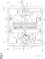
- an optical module 1A includes a substrate 2, an insulating layer 3 that is formed on the substrate 2, a semiconductor layer 4 that is formed on the insulating layer 3, and a cap 5.
- An actuator 10, a first interference optical system 20, a second interference optical system 30, and a frame part 41 are mainly formed on the substrate 2 by a part of the semiconductor layer 4.
- the frame part 41 surrounds the actuator 10, the first interference optical system 20, and the second interference optical system 30, and is fixed to the substrate 2 with the insulating layer 3 interposed therebetween.
- the optical module 1A is a MEMS device that is formed from an SOI substrate. That is, in this embodiment, the substrate 2 and the semiconductor layer 4 are made of silicon, and the insulating layer 3 is made of silicon oxide.
- the actuator 10 is an electrostatic actuator, and includes a pair of first stationary parts 11, first comb-tooth parts 12, a pair of second stationary parts 13, support parts 14, second comb-tooth parts 15, and a movable part 16.
- the pair of first stationary parts 11 is arranged in parallel in a Y-axis direction, and is fixed to the substrate 2 with the insulating layer 3 interposed therebetween.
- the first comb-tooth parts 12 are provided on one side surface of each first stationary part 11. A portion of the insulating layer 3, which is positioned directly beneath the first comb-tooth parts 12, is removed, so that the first comb-tooth parts 12 are in a state in which the first comb-tooth parts 12 float above the substrate 2.
- the first stationary parts 11 and the first comb-tooth parts 12 are integrally formed of a part of the semiconductor layer 4.
- Each of the first stationary parts 11 is provided with a first electrode 17.
- the pair of second stationary parts 13 is arranged in parallel in the Y-axis direction, and is fixed to the substrate 2 with the insulating layer 3 interposed therebetween.
- the pair of second stationary parts 13 is disposed on one side of the pair of first stationary parts 11.
- the support part 14 extends between each second stationary part 13 and the movable part 16.
- the support parts 14 are provided with the second comb-tooth parts 15 so that each of comb teeth of the comb-tooth part 15 is positioned between comb teeth of the first comb-tooth part 12.
- the movable part 16 extends in an X-axis direction so as to pass through a space formed between the pair of first stationary parts 11 and a space formed between the pair of second stationary parts 13.
- the second stationary parts 13, the support parts 14, the second comb-tooth parts 15, and the movable part 16 are integrally formed of a part of the semiconductor layer 4.
- Each of the second stationary parts 13 is provided with a second electrode 18.
- each of the support parts 14 has a structure in which leaf springs are connected, the movable part 16 can be moved in a direction (predetermined direction) A parallel to the X-axis direction.
- the support parts 14 apply an elastic force to the movable part 16 so that the movable part 16 returns to an initial position. Accordingly, when a voltage is applied between the first and second electrodes 17 and 18, electrostatic attraction acts between the first and second comb-tooth parts 12 and 15 according to the voltage (potential difference) and the movable part 16 is moved in the direction A to a position where the electrostatic attraction and the elastic force applied by the support parts 14 balance with each other.
- the first interference optical system 20 includes a first movable mirror 21, a first stationary mirror 22, and an optical block 23, and forms a Michelson interference optical system.
- First light L1 is incident on the first interference optical system 20 through a first light incident part 6, and an interference wave L10 of the first light is emitted from the first interference optical system 20 through a first light-emitting part 7.
- the first light incident part 6 and the first light-emitting part 7 are, for example, optical fibers and are fixed to the frame part 41.
- the first movable mirror 21 is provided at one end portion 16a of the movable part 16 in the direction A.
- the first movable mirror 21 includes a reflective surface 21a.
- the reflective surface 21a is a surface perpendicular to the direction A.
- the first stationary mirror 22 is provided on one side surface of the optical block 23. That is, the position of the first stationary mirror 22 is fixed.
- the first stationary mirror 22 includes a reflective surface 22a.
- the reflective surface 22a is a surface perpendicular to an X-Y plane, and is inclined with respect to the direction A at a predetermined angle.
- the optical block 23 is formed of a part of the semiconductor layer 4, and is fixed to the substrate 2 with the insulating layer 3 interposed therebetween.
- the side surface of the optical block 23 facing the first movable mirror 21 functions as a first beam splitter 23a. That is, the position of the first beam splitter 23a is fixed.
- the first beam splitter 23a is a surface perpendicular to the X-Y plane, and is inclined with respect to the direction A at an angle of 45°.
- the first light L1 which is incident on the first interference optical system 20 through the first light incident part 6, travels in the optical block 23, and is split into first light travelling to the first movable mirror 21 and first light travelling to the first stationary mirror 22 by the first beam splitter 23a.
- First light L1a split to travel to the first stationary mirror 22 is reflected by the reflective surface 22a of the first stationary mirror 22 and returns to the first beam splitter 23a along the same optical path.
- first light L1b split to travel to the first movable mirror 21 along the direction A is reflected by the reflective surface 21a of the first movable mirror 21 and returns to the first beam splitter 23a along the same optical path.
- the first light L1a and the first light L1b which return to the first beam splitter 23a, are composed by the first beam splitter 23a and form an interference wave L10 of the first light.
- the interference wave L10 of the first light is emitted from the first interference optical system 20 through the first light-emitting part 7.
- the first interference optical system 20, which obtains the interference wave L10 of the first light is adapted so that the first light L1b reciprocates one time between the first beam splitter 23a and the first movable mirror 21 along the direction A in this way.
- the second interference optical system 30 includes a second movable mirror 31, a second stationary mirror 32, and optical blocks 33 and 34, and forms a Michelson interference optical system.
- Second light L2 is incident on the second interference optical system 30 through a second light incident part 8, and an interference wave L20 of the second light is emitted from the second interference optical system 30 through a second light-emitting part 9.
- the second light incident part 8 and the second light-emitting part 9 are, for example, optical fibers and are fixed to the frame part 41.
- the second movable mirror 31 is provided at the other end portion 16b of the movable part 16 in the direction A.
- the second movable mirror 31 includes reflective surfaces 31a, 31b, and 31c.
- the reflective surface 31a is a surface perpendicular to the X-Y plane, and is inclined with respect to the direction A at an angle of 45°.
- the reflective surface 31b is a surface perpendicular to the X-Y plane, and is inclined to the side opposite to the reflective surface 31a with respect to the direction A at an angle of 45°.
- the reflective surface 31c is a surface perpendicular to the direction A.
- the second stationary mirror 32 is provided on one side surface of the optical block 33. That is, the position of the second stationary mirror 32 is fixed.
- the second stationary mirror 32 includes a reflective surface 32a.
- the reflective surface 32a is a surface perpendicular to the X-Y plane, and is inclined with respect to the direction A at a predetermined angle.
- the respective optical blocks 33 and 34 are formed of a part of the semiconductor layer 4, and are fixed to the substrate 2 with the insulating layer 3 interposed therebetween.
- the side surface of the optical block 33 facing the second movable mirror 31 functions as a second beam splitter 33a. That is, the position of the second beam splitter 33a is fixed.
- the second beam splitter 33a is a surface perpendicular to the X-Y plane, and is inclined with respect to the direction A at an angle of 45°.
- the side surface of the optical block 34 facing the second movable mirror 31 functions as a reflective surface 34a. That is, the position of the reflective surface 34a is fixed.
- the reflective surface 34a is a surface perpendicular to the X-Y plane, and is inclined to the side opposite to the second beam splitter 33a with respect to the direction A at an angle of 45°.
- the second light L2 which is incident on the second interference optical system 30 through the second light incident part 8, travels in the optical block 33, and is split into second light travelling to the second movable mirror 31 and second light travelling to the second stationary mirror 32 by the second beam splitter 33a.
- Second light L2a split to travel to the second stationary mirror 32 is reflected by the reflective surface 32a of the second stationary mirror 32 and returns to the second beam splitter 33a along the same optical path.
- second light L2b split to travel to the second movable mirror 31 along the direction A is sequentially reflected by the reflective surfaces 31a and 31b of the second movable mirror 31 and travels to the second beam splitter 33a along the direction A.
- the second light L2b which travels to the second beam splitter 33a along the direction A, is sequentially reflected by the second beam splitter 33a and the reflective surface 34a of the optical block 34, and travels to the reflective surface 31c of the second movable mirror 31 along the direction A.
- the second light L2b which travels to the reflective surface 31c along the direction A, is reflected by the reflective surface 31c, and returns to the second beam splitter 33a along the same optical path.
- the second light L2a and the second light L2b which return to the second beam splitter 33a, are composed by the second beam splitter 33a and form the interference wave L20 of the second light.
- the interference wave L20 of the second light is emitted from the second interference optical system 30 through the second light-emitting part 9.
- the second interference optical system 30, which obtains the interference wave L20 of the second light is adapted so that the second light L2b reciprocates two times between the second beam splitter 33a and the second movable mirror 31 along the direction A in this way.
- the cap 5 includes a top plate portion 51, a frame portion 52, and protruding portions 53 and 54.
- the frame portion 52 is provided on the surface of the top plate portion 51 facing the substrate 2 so as to overlap the frame part 41 when viewed in a Z-axis direction.
- the frame portion 52 is airtightly joined to the frame part 41.
- the protruding portions 53 are provided on the surface of the top plate portion 51 facing the substrate 2 so as to correspond to portions of the first stationary parts 11 that are provided with the first electrodes 17.
- the protruding portions 53 are airtightly joined to the portions of the first stationary parts 11 that are provided with the first electrodes 17.
- the protruding portions 54 are provided on the surface of the top plate portion 51 facing the substrate 2 so as to correspond to the second stationary parts 13.
- the protruding portions 54 are airtightly joined to the second stationary parts 13.
- the top plate portion 51, the frame portion 52, and the protruding portions 53 and 54 are made of, for example, silicon so as to be integrally formed.
- glass, such as quartz may be used as the materials of the top plate portion 51, the frame portion 52, and the protruding portions 53 and 54.
- Through holes 53a and 54a are formed in the cap 5.
- the through holes 53a pass through the top plate portion 51 and the protruding portions 53 along the Z-axis direction.
- the through holes 54a pass through the top plate portion 51 and the protruding portions 54 along the Z-axis direction.
- electrical contact with the first electrode 17 from the outside through the through holes 53a is realized and electrical contact with the second electrode 18 from the outside through the through holes 54a is realized.
- phase of the second light L2b in the second interference optical system 30 will be described.
- the first light L1 is split into first light travelling to the first movable mirror 21 and first light travelling to the first stationary mirror 22 by the first beam splitter 23a, and the first light L1b split to travel to the first movable mirror 21 and the first light L1a split to travel to the first stationary mirror 22 are composed by the first beam splitter 23a after the first light L1b split to travel to the first movable mirror 21 reciprocates one time along the direction A.
- the second light L2 is split into second light travelling to the second movable mirror 31 and second light travelling to the second stationary mirror 32 by the second beam splitter 33a, and the second light L2b split to travel to the second movable mirror 31 and the second light L2a split to travel to the second stationary mirror 32 are composed by the second beam splitter 33a after the second light L2b split to travel to the second movable mirror 31 reciprocates two times along the direction A. Accordingly, a phase difference occurring on the interference wave L20 of the second light is double a phase difference that occurs on the interference wave L20 of the second light in a case in which the second light L2b travelling to the second movable mirror 31 reciprocates, for example, one time along the direction A.
- the first and second movable mirrors 21 and 31 are provided on the movable part 16, the first and second movable mirrors 21 and 31 are moved along the direction A while being synchronized with each other (that is, at the same timing to the same side by the same moving distance). Accordingly, it is possible to detect the position of the first movable mirror 21 in the direction A by detecting the position of the second movable mirror 31 in the direction A on the basis of the interference wave L20 of the second light.
- the first movable mirror 21 which forms the first interference optical system 20 serving as an interference optical system for measurement, by using the first light L1 as light for measurement and using the second light L2 as light for the detection of a position as described above.
- a laser light may be used as the second light L2.
- the interference wave L20 of the second light can be efficiently obtained.
- the first movable mirror 21 is provided at one end portion 16a of the movable part 16 in the direction A and the second movable mirror 31 is provided at the other end portion 16b of the movable part 16 in the direction A. Accordingly, the movable part 16 can be moved with a good balance along the direction A.
- a laser source is connected to the light incident end of the second light incident part 8, which is an optical fiber
- a light detection element is connected to the light-emitting end of the second light-emitting part 9 that is an optical fiber. Since the light sources and the light detection elements do not need to be mounted on the optical module 1A as described above, the degree of freedom in designing the first and second interference optical systems 20 and 30 can be improved.
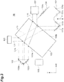
- an optical module 1B includes a movable mirror 101, stationary mirrors 102 and 104, and an optical block 103.
- components of the optical module IB, such as an actuator 10, are the same as those of the above-mentioned optical module 1A.
- the movable mirror 101 is provided at one end portion 16a (not illustrated) of the movable part 16 in a direction A parallel to a Y-axis direction.
- the movable mirror 101 includes reflective surfaces 101a, 101b, 101c, and 101d.
- the reflective surface 101a is a surface perpendicular to an X-Y plane, and is inclined with respect to the direction A at an angle of 45°.
- the reflective surface 101b is a surface perpendicular to the X-Y plane, and is inclined to the side opposite to the reflective surface 101a with respect to the direction A at an angle of 45°.
- the reflective surface 101c is a surface perpendicular to the X-Y plane, and is inclined to the side opposite to the reflective surface 101b with respect to the direction A at an angle of 45°.
- the reflective surface 101d is a surface perpendicular to the X-Y plane, and is inclined to the side opposite to the reflective surface 101c with respect to the direction A at an angle of 45°.
- the optical block 103 includes light incident/emitting surfaces 103a and 103b. Each of the light incident/emitting surfaces 103a and 103b is a surface perpendicular to the X-Y plane, and is inclined with respect to the direction A at an angle of 45°.
- the optical block 103 is formed of a part of the semiconductor layer 4, and is fixed to the substrate 2 with the insulating layer 3 interposed therebetween.
- the first light L1 which is incident through the light incident part 105, is split into first light travelling to the movable mirror 101 and first light travelling to the stationary mirror 102 by the light incident/emitting surface 103a of the optical block 103.
- First light L1a split to travel to the stationary mirror 102 is sequentially reflected by the reflective surfaces 102a and 102b of the stationary mirror 102, and is incident on the light incident/emitting surface 103a of the optical block 103.
- the first light L1a which is incident on the light incident/emitting surface 103a, travels in the optical block 103, and reaches the light incident/emitting surface 103b of the optical block 103.
- first light L1b split to travel to the movable mirror 101 travels in the optical block 103, and is emitted from the light incident/emitting surface 103b of the optical block 103.
- the first light L1b which is emitted along the direction A from the light incident/emitting surface 103b, is sequentially reflected by the reflective surfaces 101a and 101b of the movable mirror 101, and reaches the light incident/emitting surface 103b of the optical block 103 along the direction A.
- the first light L1a and the first light L1b, which reach the light incident/emitting surface 103b are composed by the light incident/emitting surface 103b, and form the interference wave L10 of the first light.
- the interference wave L10 of the first light is incident on the light-receiving element 107.
- the movable mirror 101, the stationary mirror 102, and the light incident/emitting surface 103a of the optical block 103 have the same functions as the first movable mirror 21, the first stationary mirror 22, and the first beam splitter 23a of the above-mentioned optical module 1A, respectively. That is, in this case, the movable mirror 101, the stationary mirror 102, and the optical block 103 have the same functions as the first interference optical system 20 that obtains the interference wave L10 of the first light, and allow the first light L1b to reciprocate one time between the light incident/emitting surface 103a of the optical block 103 and the movable mirror 101 along the direction A.
- the second light L2 emitted from the light-emitting element 106 is incident on the light incident/emitting surface 103a of the optical block 103 and travels in the optical block 103.
- the second light L2, which travels in the optical block 103, is split into second light travelling to the movable mirror 101 and second light travelling to the light incident/emitting surface 103a by the light incident/emitting surface 103b of the optical block 103.
- Second light L2a split to travel to the light incident/emitting surface 103a is reflected by the light incident/emitting surface 103a and reaches the light incident/emitting surface 103b of the optical block 103.
- second light L2b split to travel to the movable mirror 101 is reflected by the reflective surface 104a of the stationary mirror 104, and travels to the movable mirror 101 along the direction A.
- the second light L2b, which travels to the movable mirror 101 along the direction A, is sequentially reflected by the reflective surfaces 101d and 101c of the movable mirror 101, and travels to the stationary mirror 104 along the direction A.
- the second light L2b, which travels to the stationary mirror 104 is reflected by the reflective surface 104a of the stationary mirror 104, and travels to the light incident/emitting surface 103b of the optical block 103.
- the second light L2 is split into the second light travelling to the movable mirror 101 and the second light travelling to the light incident/emitting surface 103a of the optical block 103 by the light incident/emitting surface 103b of the optical block 103, and the second light L2b split to travel to the movable mirror 101 and the second light L2a split to travel to the light incident/emitting surface 103a are composed by the light incident/emitting surface 103b after the second light L2b split to travel to the movable mirror 101 reciprocates two times along the direction A.
- a phase difference occurring on the interference wave L20 of the second light is double a phase difference that occurs on the interference wave L20 of the second light in a case in which the second light L2b travelling to the movable mirror 101 reciprocates, for example, one time along the direction A.
- This is equivalent to the use of light having a half of a wavelength as the second light L2, and means that a resolution for the detection of a position based on the interference wave L20 of the second light is high. It is possible to accurately detect the position of the movable mirror 101, by using the first light L1 as light for measurement and using the second light L2 as light for the detection of a position as described above.
- a laser light is used as the second light L2. Accordingly, even though the number of times of reciprocation of the second light L2b, which travels to the movable mirror 101, along the direction A is increased for the further improvement of a resolution for the detection of a position based on the interference wave L20 of the second light, the interference wave L20 of the second light can be efficiently obtained.
- the movable mirror 101 since the movable mirror 101 is provided at one end portion 16a of the movable part 16 in the direction A in the optical module 1B, the movable mirror 101 has a structure equivalent to a structure in which the first and second movable mirrors 21 and 31 of the above-mentioned optical module 1A share at least a part thereof. Accordingly, the optical module 1B can be reduced in size.
- the position of the movable mirror (first movable mirror 21, movable mirror 101) is detected on the basis of an interference wave of a laser light (the interference wave L20 of the second light).
- a method of detecting the position of the movable mirror there are a voltage monitoring method and an electrostatic capacity monitoring method other than a method of monitoring a laser light that is used in the above-mentioned first and second embodiments.
- the voltage monitoring method is a method of detecting the position of the movable mirror on the basis of a voltage that is applied between the first and second electrodes 17 and 18.
- the moving distance of the movable mirror is proportional to the square of a voltage. Accordingly, since the moving distance becomes sensitive to a voltage as the moving distance is increased, a voltage needs to be more accurately detected.
- the position of the movable mirror is hard to be calculated with the same accuracy over the entire movable range of the movable mirror has been described, but problems in principle are also present.
- the amplitude (moving distance) and phase of the resonant operation do not completely coincide with an applied voltage. That is, even though the applied voltage is monitored, the movable mirror does not perform an operation corresponding to the applied voltage.
- the actuator 10 In a Fourier transform-type infrared spectrometer (hereinafter, referred to as a "MEMS-FTIR") in which a MEMS technology is used, the actuator 10 is generally operated at a resonant frequency or a frequency close to the resonant frequency.
- MEMS-FTIR Fourier transform-type infrared spectrometer
- the actuator 10 is generally operated at a resonant frequency or a frequency close to the resonant frequency.
- the reason for this is that the applied voltage can be reduced and measurement time can be shortened (alternatively, the reason for this is that the number of samples to be capable of being measured in the same time can be increased, which results in the improvement of an S/N ratio). Accordingly, the voltage monitoring method is generally not helpful in the MEMS-FTIR.
- an electrostatic capacity monitoring method is a method of detecting the position of the movable mirror on the basis of electrostatic capacity that is formed between the first and second comb-tooth parts 12 and 15. Since the electrostatic capacity monitoring method can be realized through only the formation of an electronic circuit and does not require the addition of a structure to the MEMS device, the electrostatic capacity monitoring method is presently employed in many MEMS devices. However, there is also a problem in the electrostatic capacity monitoring method.
- the moving distance of a movable mirror is about 250 ⁇ m, that is, is about 500 ⁇ m as an optical path length (OPD).
- OPD optical path length
- the laser light monitoring method is a method of detecting the position of the movable mirror on the basis of the interference wave of the laser light.
- the laser light monitoring method has been employed in a stationary Fourier transform-type infrared spectrometer (hereinafter, referred to as a "stationary FTIR"), but has not been employed in the MEMS-FTIR. The reason for this is as follows.
- sampling points can be determined at an interval of ⁇ L /2 when a laser light having a wavelength ⁇ L is used.
- a zero-cross point may be used as a trigger to sample an actual signal.
- sampling theorem is a theorem where data needs to be sampled at a frequency that is equal to or larger than double the maximum wave number to be required in a case in which original signals are accurately reproduced from discrete data sampled at regular intervals.
- the wavelength ⁇ L of a laser light required in this case should be 1 ⁇ m or less.
- the side surface of an optical block made of silicon is used as a beam splitter and a split laser light travels in the optical block made of silicon.
- a laser light having a wavelength of 1.1 ⁇ m or less is absorbed by the optical block.
- the minimum value of the wavelength of a laser light, which can be used in the MEMS-FTIR is 1.1 ⁇ m.
- an interference optical system for detecting a position (second interference optical system 30) is adapted so that a laser light reciprocates two or more times between the beam splitter and the movable mirror along the movable direction of the movable mirror.
- This means is equivalent to the use of a laser light having a shorter wavelength, and means that a resolution for the detection of a position based on an interference wave of a laser light is high.
- the light for measurement (first light L1) is incident and measurement is performed to acquire a measurement signal.
- the measurement signal is corrected on the basis of the calibration data acquired in advance, a correct spectrum can be obtained.
- a procedure for acquiring calibration data at regular intervals or the like is determined as necessary, data can be more stably acquired.
- the spectrum of a calibration signal appears in a region different from the spectrum of a measurement signal as illustrated in FIG. 6 even though the laser light for calibration (second light L2) is turned on during measurement.
- a spectrum indicated as a laser light is the spectrum of the calibration signal and a spectrum indicated as white light is the spectrum of the measurement signal.
- the spectrum of a calibration signal appears at 0.65 ⁇ m (a wave number of 15385 cm -1 ) that is a position corresponding to a half of the wavelength of the laser light for calibration (double in the wave number).
- the spectrum of the calibration signal appears in a region different from the spectrum of the measurement signal (a detection wavelength range as the MEMS-FTIR) in this way, the spectrum of the calibration signal and the spectrum of the measurement signal can be easily separated from each other. Also in the example of calibration for performing calibration before measurement and monitoring the stability of measurement, as in the example of calibration to be performed before measurement, calibration data is acquired in a stage supposed as the same environments as that during measurement and the calibration data is used during measurement.
- the shape of the spectrum of a calibration signal at the time of occurrence of an error is to be noted.
- a central wavelength deviates, an amplitude is reduced, and the half-value width of a spectrum is increased, but there is no influence thereof on a measurement wavelength range.
- an error also occurs on the spectrum of the measurement signal, but there is no influence thereof on the spectrum of the calibration signal.
- the component of the measurement signal and the component of the calibration signal can be separated from each other on the spectrum even in a case in which an error occurs in calibration.
- spectrum data is separated in this state and only data of the component of the calibration signal is subjected to inverse Fourier transform again by using the data of the calibration signal including an error, the real-time data of only the calibration signal can be acquired.
- a case in which the spectrum of an original calibration signal is not obtained means that the degree of a deviation is large and the component of the calibration signal obtained using calibration data including an error is mixed to the component of the measurement signal and cannot be separated completely. In such a case, it is necessary to warn a measurer to perform recalibration.
- a case in which a deviation large enough not to be recalibrated occurs means a case in which a phenomenon, which is not supposed, such as vibration or impact, occurs.
- the case of an environment where such a phenomenon frequently occurs is out of the range of specifications, and only data corresponding to an unexpected phenomenon has only to be deleted in the case of the unexpected phenomenon. If the measurement signal and the calibration signal are simultaneously monitored even in this case, the generation of abnormality can be detected in real time.
- the first interference optical system may be adapted so that the first light reciprocates m times (m is a natural number) between the first beam splitter and the first movable mirror along a predetermined direction (the movable direction of the movable part), and the second interference optical system may be adapted so that the second light reciprocates n times (n is a natural number greater than m) between the second beam splitter and the second movable mirror along a predetermined direction (the movable direction of the movable part).
- the interference wave L10 of the first light and the interference wave L20 of the second light can be separately acquired in the optical module 1A of the first embodiment, the interference wave L10 of the first light can be subjected to analog processing. Specifically, the interference wave L10 of the first light is allowed to pass through a high-pass filter first so that a DC component is cut. Subsequently, a rectangular signal, which is changed at points where the value of the signal is switched to a minus from a plus or to a plus from a minus, is obtained through a comparator. Then, the A/D conversion data of the measurement signal may be triggered by the rise and fall of the rectangular signal.
- the optical module 1A of the first embodiment may include a light-emitting element outputting the second light L2 and a light-receiving element detecting the interference wave L20 of the second light instead of the second light incident part 8 and the second light-emitting part 9, and may further include a white light source, which outputs the first light L1, as the light-emitting element for measurement instead of the first light incident part 6.
- a measurement sample is irradiated with the interference wave L10 of the first light, which is output from the first light-emitting part 7, and a reflected wave or a transmitted wave of the interference wave L10 of the first light is received by a light-receiving element that is prepared outside.
- the optical module 1A can be easily handled. Meanwhile, the interference wave L10 of the first light is received by a light-receiving element that is prepared outside. For this reason, the need to mount the light-receiving element, which detects the interference wave L10 of the first light, on the optical module 1A is low.
- the optical module 1A of the first embodiment may include a light-emitting element outputting the second light L2 and a light-receiving element detecting the interference wave L20 of the second light instead of the second light incident part 8 and the second light-emitting part 9, and may further include a light-receiving element detecting the interference wave L10 of the first light instead of the first light-emitting part 7.
- a measurement sample is irradiated with the first light L1, which is output from the white light source prepared outside as the light-emitting element for measurement, and a reflected wave or a transmitted wave of the first light L1 is received by the light-receiving element through the first light incident part 6 and the first interference optical system 20.
- the optical module 1A since the light-emitting element outputting the second light L2, the light-receiving element detecting the interference wave L20 of the second light, and the light-receiving element detecting the interference wave L10 of the first light are mounted on the optical module 1A, the optical module 1A can be easily handled. Meanwhile, the first light L1 is output from the white light source that is prepared outside as the light-emitting element for measurement. For this reason, the need to mount the light-emitting element for measurement on the optical module 1A is low.
- the optical module 1B of the second embodiment may further include a second light incident part, which allows the second light L2 to be incident, and a light-emitting part, which emits the interference wave L10 of the first light and the interference wave L20 of the second light, instead of the light-emitting element 106 and the light-receiving element 107.
- a white light source is connected to the light incident end of the light incident part 105 that is an optical fiber
- a laser source is connected to the light incident end of the second light incident part that is an optical fiber
- a light detection element is connected to the light-emitting end of the light-emitting part that is an optical fiber. Since the light sources and the light detection elements do not need to be mounted on the optical module 1B as described above, the degree of freedom in designing the interference optical systems (first and second interference optical systems) can be improved.
- first through-electrode electrically connected to each first stationary part 11 and a second through-electrode electrically connected to each second stationary part 13 may be provided on the substrate 2 and the insulating layer 3, and a voltage may be applied between the first and second through-electrodes.
- the actuator 10 is not limited to an electrostatic actuator, and may be, for example, a piezoelectric actuator, an electromagnetic actuator, or the like.
Landscapes
- Physics & Mathematics (AREA)
- Spectroscopy & Molecular Physics (AREA)
- General Physics & Mathematics (AREA)
- Optics & Photonics (AREA)
- Spectrometry And Color Measurement (AREA)
- Mechanical Light Control Or Optical Switches (AREA)
- Length Measuring Devices By Optical Means (AREA)
- Instruments For Measurement Of Length By Optical Means (AREA)
Applications Claiming Priority (2)
| Application Number | Priority Date | Filing Date | Title |
|---|---|---|---|
| JP2016017956A JP6628622B2 (ja) | 2016-02-02 | 2016-02-02 | 光モジュール |
| PCT/JP2017/003727 WO2017135357A1 (ja) | 2016-02-02 | 2017-02-02 | 光モジュール |
Publications (3)
| Publication Number | Publication Date |
|---|---|
| EP3413012A1 true EP3413012A1 (de) | 2018-12-12 |
| EP3413012A4 EP3413012A4 (de) | 2019-09-11 |
| EP3413012B1 EP3413012B1 (de) | 2022-08-17 |
Family
ID=59501014
Family Applications (1)
| Application Number | Title | Priority Date | Filing Date |
|---|---|---|---|
| EP17747508.4A Active EP3413012B1 (de) | 2016-02-02 | 2017-02-02 | Optisches modul |
Country Status (5)
| Country | Link |
|---|---|
| US (1) | US10422696B2 (de) |
| EP (1) | EP3413012B1 (de) |
| JP (1) | JP6628622B2 (de) |
| CN (1) | CN108603747B (de) |
| WO (1) | WO2017135357A1 (de) |
Families Citing this family (7)
| Publication number | Priority date | Publication date | Assignee | Title |
|---|---|---|---|---|
| JP6704833B2 (ja) * | 2016-10-27 | 2020-06-03 | 浜松ホトニクス株式会社 | 位置検出方法及び光モジュール |
| WO2019009402A1 (ja) | 2017-07-06 | 2019-01-10 | 浜松ホトニクス株式会社 | 光学デバイス |
| EP3653109A4 (de) | 2017-07-14 | 2020-07-15 | Public University Corporation Yokohama City University | Vorrichtung zur verschlechterungsabschätzung und programm zur verschlechterungsabschätzung |
| US10770327B2 (en) | 2017-07-28 | 2020-09-08 | Taiwan Semiconductor Manufacturing Co., Ltd. | System and method for correcting non-ideal wafer topography |
| US11085825B2 (en) | 2018-03-30 | 2021-08-10 | Si-Ware Systems | Self-referenced spectrometer |
| JP6688917B1 (ja) | 2019-01-30 | 2020-04-28 | 浜松ホトニクス株式会社 | 光モジュール、信号処理システム及び信号処理方法 |
| JP2024017359A (ja) * | 2022-07-27 | 2024-02-08 | セイコーエプソン株式会社 | 光学デバイスおよび分光装置 |
Family Cites Families (10)
| Publication number | Priority date | Publication date | Assignee | Title |
|---|---|---|---|---|
| US4537508A (en) * | 1983-03-01 | 1985-08-27 | Laser Precision Corporation | Interferometer spectrometer having improved scanning reference point |
| JPH0346523A (ja) * | 1989-07-14 | 1991-02-27 | Sumitomo Electric Ind Ltd | フーリェ変換型分光器用信号処理装置 |
| JP2005274550A (ja) * | 2003-09-03 | 2005-10-06 | Ricoh Co Ltd | レーザー測長器及び光ディスク原盤露光装置 |
| AT413765B (de) * | 2004-06-24 | 2006-05-15 | Ctr Carinthian Tech Res Ag | Anordnung zum aufbau eines miniaturisierten fourier-transform-interferometers für optische strahlung nach dem michelson- bzw. einem daraus abgeleiteten prinzip |
| DE102005046605A1 (de) * | 2005-09-29 | 2007-04-05 | Robert Bosch Gmbh | Interferometrische Messeinrichtung |
| US8508745B2 (en) * | 2006-09-28 | 2013-08-13 | Si-Ware Systems | System, method and apparatus for a micromachined interferometer using optical splitting |
| JP5302020B2 (ja) * | 2009-01-26 | 2013-10-02 | 浜松ホトニクス株式会社 | 光モジュール |
| JP2011038829A (ja) * | 2009-08-07 | 2011-02-24 | Topcon Corp | 干渉顕微鏡及び測定装置 |
| EP2545406B1 (de) | 2010-03-09 | 2015-02-11 | SI-Ware Systems | Verfahren zur bestimmung der spiegelposition in optischen interferometern |
| JP6704833B2 (ja) * | 2016-10-27 | 2020-06-03 | 浜松ホトニクス株式会社 | 位置検出方法及び光モジュール |
-
2016
- 2016-02-02 JP JP2016017956A patent/JP6628622B2/ja active Active
-
2017
- 2017-02-02 US US16/072,634 patent/US10422696B2/en active Active
- 2017-02-02 CN CN201780009338.5A patent/CN108603747B/zh active Active
- 2017-02-02 EP EP17747508.4A patent/EP3413012B1/de active Active
- 2017-02-02 WO PCT/JP2017/003727 patent/WO2017135357A1/ja not_active Ceased
Also Published As
| Publication number | Publication date |
|---|---|
| CN108603747A (zh) | 2018-09-28 |
| WO2017135357A1 (ja) | 2017-08-10 |
| JP6628622B2 (ja) | 2020-01-15 |
| EP3413012B1 (de) | 2022-08-17 |
| CN108603747B (zh) | 2020-08-18 |
| JP2017138390A (ja) | 2017-08-10 |
| US10422696B2 (en) | 2019-09-24 |
| EP3413012A4 (de) | 2019-09-11 |
| US20190033136A1 (en) | 2019-01-31 |
Similar Documents
| Publication | Publication Date | Title |
|---|---|---|
| EP3413012B1 (de) | Optisches modul | |
| US11782263B2 (en) | Capacitive charge based self-sensing and position observer for electrostatic MEMS mirrors | |
| JP6306820B2 (ja) | 光学干渉計におけるミラー位置を決定する技法 | |
| KR101566383B1 (ko) | 기하학적 두께와 굴절률 측정을 위한 반사형 광섬유 간섭 장치 | |
| KR102340495B1 (ko) | 스펙트럼 분석을 사용하는 간섭측정식 인코더 | |
| WO2011091012A2 (en) | Interferometer with variable optical path length reference mirror and applications thereof | |
| Ishikawa et al. | Integrated micro-displacement sensor that measures tilting angle and linear movement of an external mirror | |
| US10557755B2 (en) | Position detection method and optical module | |
| JP6386477B2 (ja) | 光mems干渉計におけるミラー位置の自己校正 | |
| CN102906534A (zh) | 用于物理参数的光学测量的设备 | |
| EP0197221A1 (de) | Vorrichtung zum Messen der Lage eines Objektes | |
| JP4403272B2 (ja) | 分光計測方法及び分光計測装置 | |
| JP6391155B2 (ja) | 絶対角測定装置及び絶対角測定方法 | |
| US20250102362A1 (en) | Interferometer | |
| JP5891955B2 (ja) | フーリエ変換型分光計用タイミング生成装置および該生成方法ならびにフーリエ変換型分光計および該分光方法 | |
| US6618150B2 (en) | Compact transform spectrometer based on sampling a standing wave | |
| Pocha et al. | Miniature accelerometer and multichannel signal processor for fiberoptic Fabry–Pérot sensing | |
| JP2005345230A (ja) | 光干渉型センサ | |
| Annovazzi-Lodi et al. | Spot optical measurements on micromachined mirrors for photonic switching | |
| JP3919796B2 (ja) | 変位測定装置 | |
| Ortlepp et al. | Ultrathin transparent photodetector for use in Standing-Wave Interferometer | |
| Tortschanoff et al. | Optical position feedback of quasi-static 2D MOEMS mirrors | |
| Ortlepp et al. | Phase-Modulated Standing Wave Interferometer. Micromachines 2021, 12, 357 | |
| JP2000131027A (ja) | 寸法測定装置 | |
| Lenzhofer et al. | Position encoding and closed loop control of MOEMS translatory actuators |
Legal Events
| Date | Code | Title | Description |
|---|---|---|---|
| STAA | Information on the status of an ep patent application or granted ep patent |
Free format text: STATUS: THE INTERNATIONAL PUBLICATION HAS BEEN MADE |
|
| PUAI | Public reference made under article 153(3) epc to a published international application that has entered the european phase |
Free format text: ORIGINAL CODE: 0009012 |
|
| STAA | Information on the status of an ep patent application or granted ep patent |
Free format text: STATUS: REQUEST FOR EXAMINATION WAS MADE |
|
| 17P | Request for examination filed |
Effective date: 20180706 |
|
| AK | Designated contracting states |
Kind code of ref document: A1 Designated state(s): AL AT BE BG CH CY CZ DE DK EE ES FI FR GB GR HR HU IE IS IT LI LT LU LV MC MK MT NL NO PL PT RO RS SE SI SK SM TR |
|
| AX | Request for extension of the european patent |
Extension state: BA ME |
|
| DAV | Request for validation of the european patent (deleted) | ||
| DAX | Request for extension of the european patent (deleted) | ||
| A4 | Supplementary search report drawn up and despatched |
Effective date: 20190814 |
|
| RIC1 | Information provided on ipc code assigned before grant |
Ipc: G02B 26/06 20060101ALI20190808BHEP Ipc: G01B 9/02 20060101ALI20190808BHEP Ipc: G01J 3/45 20060101ALI20190808BHEP Ipc: G01J 3/02 20060101ALI20190808BHEP Ipc: G01B 11/00 20060101AFI20190808BHEP Ipc: G01J 3/06 20060101ALI20190808BHEP Ipc: B81B 5/00 20060101ALI20190808BHEP |
|
| GRAP | Despatch of communication of intention to grant a patent |
Free format text: ORIGINAL CODE: EPIDOSNIGR1 |
|
| STAA | Information on the status of an ep patent application or granted ep patent |
Free format text: STATUS: GRANT OF PATENT IS INTENDED |
|
| INTG | Intention to grant announced |
Effective date: 20220324 |
|
| GRAS | Grant fee paid |
Free format text: ORIGINAL CODE: EPIDOSNIGR3 |
|
| GRAA | (expected) grant |
Free format text: ORIGINAL CODE: 0009210 |
|
| STAA | Information on the status of an ep patent application or granted ep patent |
Free format text: STATUS: THE PATENT HAS BEEN GRANTED |
|
| AK | Designated contracting states |
Kind code of ref document: B1 Designated state(s): AL AT BE BG CH CY CZ DE DK EE ES FI FR GB GR HR HU IE IS IT LI LT LU LV MC MK MT NL NO PL PT RO RS SE SI SK SM TR |
|
| REG | Reference to a national code |
Ref country code: CH Ref legal event code: EP |
|
| REG | Reference to a national code |
Ref country code: DE Ref legal event code: R096 Ref document number: 602017060753 Country of ref document: DE |
|
| REG | Reference to a national code |
Ref country code: IE Ref legal event code: FG4D |
|
| REG | Reference to a national code |
Ref country code: AT Ref legal event code: REF Ref document number: 1512450 Country of ref document: AT Kind code of ref document: T Effective date: 20220915 |
|
| REG | Reference to a national code |
Ref country code: NL Ref legal event code: MP Effective date: 20220817 |
|
| REG | Reference to a national code |
Ref country code: LT Ref legal event code: MG9D |
|
| PG25 | Lapsed in a contracting state [announced via postgrant information from national office to epo] |
Ref country code: SE Free format text: LAPSE BECAUSE OF FAILURE TO SUBMIT A TRANSLATION OF THE DESCRIPTION OR TO PAY THE FEE WITHIN THE PRESCRIBED TIME-LIMIT Effective date: 20220817 Ref country code: RS Free format text: LAPSE BECAUSE OF FAILURE TO SUBMIT A TRANSLATION OF THE DESCRIPTION OR TO PAY THE FEE WITHIN THE PRESCRIBED TIME-LIMIT Effective date: 20220817 Ref country code: PT Free format text: LAPSE BECAUSE OF FAILURE TO SUBMIT A TRANSLATION OF THE DESCRIPTION OR TO PAY THE FEE WITHIN THE PRESCRIBED TIME-LIMIT Effective date: 20221219 Ref country code: NO Free format text: LAPSE BECAUSE OF FAILURE TO SUBMIT A TRANSLATION OF THE DESCRIPTION OR TO PAY THE FEE WITHIN THE PRESCRIBED TIME-LIMIT Effective date: 20221117 Ref country code: NL Free format text: LAPSE BECAUSE OF FAILURE TO SUBMIT A TRANSLATION OF THE DESCRIPTION OR TO PAY THE FEE WITHIN THE PRESCRIBED TIME-LIMIT Effective date: 20220817 Ref country code: LV Free format text: LAPSE BECAUSE OF FAILURE TO SUBMIT A TRANSLATION OF THE DESCRIPTION OR TO PAY THE FEE WITHIN THE PRESCRIBED TIME-LIMIT Effective date: 20220817 Ref country code: LT Free format text: LAPSE BECAUSE OF FAILURE TO SUBMIT A TRANSLATION OF THE DESCRIPTION OR TO PAY THE FEE WITHIN THE PRESCRIBED TIME-LIMIT Effective date: 20220817 Ref country code: FI Free format text: LAPSE BECAUSE OF FAILURE TO SUBMIT A TRANSLATION OF THE DESCRIPTION OR TO PAY THE FEE WITHIN THE PRESCRIBED TIME-LIMIT Effective date: 20220817 |
|
| REG | Reference to a national code |
Ref country code: AT Ref legal event code: MK05 Ref document number: 1512450 Country of ref document: AT Kind code of ref document: T Effective date: 20220817 |
|
| PG25 | Lapsed in a contracting state [announced via postgrant information from national office to epo] |
Ref country code: PL Free format text: LAPSE BECAUSE OF FAILURE TO SUBMIT A TRANSLATION OF THE DESCRIPTION OR TO PAY THE FEE WITHIN THE PRESCRIBED TIME-LIMIT Effective date: 20220817 Ref country code: IS Free format text: LAPSE BECAUSE OF FAILURE TO SUBMIT A TRANSLATION OF THE DESCRIPTION OR TO PAY THE FEE WITHIN THE PRESCRIBED TIME-LIMIT Effective date: 20221217 Ref country code: HR Free format text: LAPSE BECAUSE OF FAILURE TO SUBMIT A TRANSLATION OF THE DESCRIPTION OR TO PAY THE FEE WITHIN THE PRESCRIBED TIME-LIMIT Effective date: 20220817 Ref country code: GR Free format text: LAPSE BECAUSE OF FAILURE TO SUBMIT A TRANSLATION OF THE DESCRIPTION OR TO PAY THE FEE WITHIN THE PRESCRIBED TIME-LIMIT Effective date: 20221118 |
|
| PG25 | Lapsed in a contracting state [announced via postgrant information from national office to epo] |
Ref country code: SM Free format text: LAPSE BECAUSE OF FAILURE TO SUBMIT A TRANSLATION OF THE DESCRIPTION OR TO PAY THE FEE WITHIN THE PRESCRIBED TIME-LIMIT Effective date: 20220817 Ref country code: RO Free format text: LAPSE BECAUSE OF FAILURE TO SUBMIT A TRANSLATION OF THE DESCRIPTION OR TO PAY THE FEE WITHIN THE PRESCRIBED TIME-LIMIT Effective date: 20220817 Ref country code: ES Free format text: LAPSE BECAUSE OF FAILURE TO SUBMIT A TRANSLATION OF THE DESCRIPTION OR TO PAY THE FEE WITHIN THE PRESCRIBED TIME-LIMIT Effective date: 20220817 Ref country code: DK Free format text: LAPSE BECAUSE OF FAILURE TO SUBMIT A TRANSLATION OF THE DESCRIPTION OR TO PAY THE FEE WITHIN THE PRESCRIBED TIME-LIMIT Effective date: 20220817 Ref country code: CZ Free format text: LAPSE BECAUSE OF FAILURE TO SUBMIT A TRANSLATION OF THE DESCRIPTION OR TO PAY THE FEE WITHIN THE PRESCRIBED TIME-LIMIT Effective date: 20220817 Ref country code: AT Free format text: LAPSE BECAUSE OF FAILURE TO SUBMIT A TRANSLATION OF THE DESCRIPTION OR TO PAY THE FEE WITHIN THE PRESCRIBED TIME-LIMIT Effective date: 20220817 |
|
| REG | Reference to a national code |
Ref country code: DE Ref legal event code: R097 Ref document number: 602017060753 Country of ref document: DE |
|
| PG25 | Lapsed in a contracting state [announced via postgrant information from national office to epo] |
Ref country code: SK Free format text: LAPSE BECAUSE OF FAILURE TO SUBMIT A TRANSLATION OF THE DESCRIPTION OR TO PAY THE FEE WITHIN THE PRESCRIBED TIME-LIMIT Effective date: 20220817 Ref country code: EE Free format text: LAPSE BECAUSE OF FAILURE TO SUBMIT A TRANSLATION OF THE DESCRIPTION OR TO PAY THE FEE WITHIN THE PRESCRIBED TIME-LIMIT Effective date: 20220817 |
|
| P01 | Opt-out of the competence of the unified patent court (upc) registered |
Effective date: 20230509 |
|
| PLBE | No opposition filed within time limit |
Free format text: ORIGINAL CODE: 0009261 |
|
| STAA | Information on the status of an ep patent application or granted ep patent |
Free format text: STATUS: NO OPPOSITION FILED WITHIN TIME LIMIT |
|
| PG25 | Lapsed in a contracting state [announced via postgrant information from national office to epo] |
Ref country code: AL Free format text: LAPSE BECAUSE OF FAILURE TO SUBMIT A TRANSLATION OF THE DESCRIPTION OR TO PAY THE FEE WITHIN THE PRESCRIBED TIME-LIMIT Effective date: 20220817 |
|
| 26N | No opposition filed |
Effective date: 20230519 |
|
| PG25 | Lapsed in a contracting state [announced via postgrant information from national office to epo] |
Ref country code: SI Free format text: LAPSE BECAUSE OF FAILURE TO SUBMIT A TRANSLATION OF THE DESCRIPTION OR TO PAY THE FEE WITHIN THE PRESCRIBED TIME-LIMIT Effective date: 20220817 |
|
| PG25 | Lapsed in a contracting state [announced via postgrant information from national office to epo] |
Ref country code: MC Free format text: LAPSE BECAUSE OF FAILURE TO SUBMIT A TRANSLATION OF THE DESCRIPTION OR TO PAY THE FEE WITHIN THE PRESCRIBED TIME-LIMIT Effective date: 20220817 |
|
| REG | Reference to a national code |
Ref country code: CH Ref legal event code: PL |
|
| REG | Reference to a national code |
Ref country code: BE Ref legal event code: MM Effective date: 20230228 |
|
| PG25 | Lapsed in a contracting state [announced via postgrant information from national office to epo] |
Ref country code: LU Free format text: LAPSE BECAUSE OF NON-PAYMENT OF DUE FEES Effective date: 20230202 Ref country code: LI Free format text: LAPSE BECAUSE OF NON-PAYMENT OF DUE FEES Effective date: 20230228 Ref country code: CH Free format text: LAPSE BECAUSE OF NON-PAYMENT OF DUE FEES Effective date: 20230228 |
|
| REG | Reference to a national code |
Ref country code: IE Ref legal event code: MM4A |
|
| PG25 | Lapsed in a contracting state [announced via postgrant information from national office to epo] |
Ref country code: IE Free format text: LAPSE BECAUSE OF NON-PAYMENT OF DUE FEES Effective date: 20230202 |
|
| PG25 | Lapsed in a contracting state [announced via postgrant information from national office to epo] |
Ref country code: BE Free format text: LAPSE BECAUSE OF NON-PAYMENT OF DUE FEES Effective date: 20230228 |
|
| PG25 | Lapsed in a contracting state [announced via postgrant information from national office to epo] |
Ref country code: IT Free format text: LAPSE BECAUSE OF FAILURE TO SUBMIT A TRANSLATION OF THE DESCRIPTION OR TO PAY THE FEE WITHIN THE PRESCRIBED TIME-LIMIT Effective date: 20220817 |
|
| PG25 | Lapsed in a contracting state [announced via postgrant information from national office to epo] |
Ref country code: BG Free format text: LAPSE BECAUSE OF FAILURE TO SUBMIT A TRANSLATION OF THE DESCRIPTION OR TO PAY THE FEE WITHIN THE PRESCRIBED TIME-LIMIT Effective date: 20220817 |
|
| PG25 | Lapsed in a contracting state [announced via postgrant information from national office to epo] |
Ref country code: BG Free format text: LAPSE BECAUSE OF FAILURE TO SUBMIT A TRANSLATION OF THE DESCRIPTION OR TO PAY THE FEE WITHIN THE PRESCRIBED TIME-LIMIT Effective date: 20220817 |
|
| PGFP | Annual fee paid to national office [announced via postgrant information from national office to epo] |
Ref country code: GB Payment date: 20241227 Year of fee payment: 9 |
|
| PGFP | Annual fee paid to national office [announced via postgrant information from national office to epo] |
Ref country code: FR Payment date: 20241231 Year of fee payment: 9 |
|
| PGFP | Annual fee paid to national office [announced via postgrant information from national office to epo] |
Ref country code: DE Payment date: 20241231 Year of fee payment: 9 |
|
| PG25 | Lapsed in a contracting state [announced via postgrant information from national office to epo] |
Ref country code: CY Free format text: LAPSE BECAUSE OF FAILURE TO SUBMIT A TRANSLATION OF THE DESCRIPTION OR TO PAY THE FEE WITHIN THE PRESCRIBED TIME-LIMIT; INVALID AB INITIO Effective date: 20170202 |
|
| PG25 | Lapsed in a contracting state [announced via postgrant information from national office to epo] |
Ref country code: HU Free format text: LAPSE BECAUSE OF FAILURE TO SUBMIT A TRANSLATION OF THE DESCRIPTION OR TO PAY THE FEE WITHIN THE PRESCRIBED TIME-LIMIT; INVALID AB INITIO Effective date: 20170202 |
|
| PG25 | Lapsed in a contracting state [announced via postgrant information from national office to epo] |
Ref country code: TR Free format text: LAPSE BECAUSE OF FAILURE TO SUBMIT A TRANSLATION OF THE DESCRIPTION OR TO PAY THE FEE WITHIN THE PRESCRIBED TIME-LIMIT Effective date: 20220817 |