EP3416181A1 - Röntgenstrahlquelle und verfahren zur herstellung einer röntgenstrahlquelle - Google Patents
Röntgenstrahlquelle und verfahren zur herstellung einer röntgenstrahlquelle Download PDFInfo
- Publication number
- EP3416181A1 EP3416181A1 EP17176243.8A EP17176243A EP3416181A1 EP 3416181 A1 EP3416181 A1 EP 3416181A1 EP 17176243 A EP17176243 A EP 17176243A EP 3416181 A1 EP3416181 A1 EP 3416181A1
- Authority
- EP
- European Patent Office
- Prior art keywords
- insulator
- cooling channel
- ray source
- emitter arrangement
- feedthrough
- Prior art date
- Legal status (The legal status is an assumption and is not a legal conclusion. Google has not performed a legal analysis and makes no representation as to the accuracy of the status listed.)
- Withdrawn
Links
- 238000000034 method Methods 0.000 title claims description 15
- 238000004519 manufacturing process Methods 0.000 title claims description 11
- 239000012212 insulator Substances 0.000 claims abstract description 198
- 238000001816 cooling Methods 0.000 claims abstract description 187
- 239000000463 material Substances 0.000 claims description 40
- 239000002826 coolant Substances 0.000 claims description 25
- 238000003384 imaging method Methods 0.000 claims description 18
- 239000000919 ceramic Substances 0.000 claims description 13
- 238000004026 adhesive bonding Methods 0.000 claims description 7
- 239000012530 fluid Substances 0.000 claims description 7
- 238000005245 sintering Methods 0.000 claims description 7
- 238000010146 3D printing Methods 0.000 claims description 6
- 238000010894 electron beam technology Methods 0.000 claims description 6
- PNEYBMLMFCGWSK-UHFFFAOYSA-N aluminium oxide Inorganic materials [O-2].[O-2].[O-2].[Al+3].[Al+3] PNEYBMLMFCGWSK-UHFFFAOYSA-N 0.000 claims description 5
- 238000010926 purge Methods 0.000 claims description 5
- 239000000203 mixture Substances 0.000 claims description 3
- 239000000126 substance Substances 0.000 claims description 3
- 239000002184 metal Substances 0.000 description 10
- 229910052751 metal Inorganic materials 0.000 description 10
- 238000012546 transfer Methods 0.000 description 5
- 238000004891 communication Methods 0.000 description 4
- XLYOFNOQVPJJNP-UHFFFAOYSA-N water Substances O XLYOFNOQVPJJNP-UHFFFAOYSA-N 0.000 description 4
- 150000002148 esters Chemical class 0.000 description 3
- 239000003921 oil Substances 0.000 description 3
- 239000004033 plastic Substances 0.000 description 3
- RYGMFSIKBFXOCR-UHFFFAOYSA-N Copper Chemical compound [Cu] RYGMFSIKBFXOCR-UHFFFAOYSA-N 0.000 description 2
- XUIMIQQOPSSXEZ-UHFFFAOYSA-N Silicon Chemical compound [Si] XUIMIQQOPSSXEZ-UHFFFAOYSA-N 0.000 description 2
- 230000001133 acceleration Effects 0.000 description 2
- 238000002591 computed tomography Methods 0.000 description 2
- 229910052802 copper Inorganic materials 0.000 description 2
- 239000010949 copper Substances 0.000 description 2
- 230000001419 dependent effect Effects 0.000 description 2
- 230000000694 effects Effects 0.000 description 2
- 239000011521 glass Substances 0.000 description 2
- 239000008187 granular material Substances 0.000 description 2
- 230000017525 heat dissipation Effects 0.000 description 2
- 239000007788 liquid Substances 0.000 description 2
- 235000012771 pancakes Nutrition 0.000 description 2
- 239000002245 particle Substances 0.000 description 2
- 229920001296 polysiloxane Polymers 0.000 description 2
- 229910052710 silicon Inorganic materials 0.000 description 2
- 239000010703 silicon Substances 0.000 description 2
- LFQSCWFLJHTTHZ-UHFFFAOYSA-N Ethanol Chemical compound CCO LFQSCWFLJHTTHZ-UHFFFAOYSA-N 0.000 description 1
- 238000010276 construction Methods 0.000 description 1
- 238000013461 design Methods 0.000 description 1
- 229920001971 elastomer Polymers 0.000 description 1
- 230000005684 electric field Effects 0.000 description 1
- 239000007769 metal material Substances 0.000 description 1
- 238000007639 printing Methods 0.000 description 1
- 238000012545 processing Methods 0.000 description 1
- 238000001959 radiotherapy Methods 0.000 description 1
- 239000011226 reinforced ceramic Substances 0.000 description 1
- 238000009877 rendering Methods 0.000 description 1
- 229920002379 silicone rubber Polymers 0.000 description 1
- 239000004945 silicone rubber Substances 0.000 description 1
- 230000008646 thermal stress Effects 0.000 description 1
Images


Classifications
-
- H—ELECTRICITY
- H01—ELECTRIC ELEMENTS
- H01J—ELECTRIC DISCHARGE TUBES OR DISCHARGE LAMPS
- H01J35/00—X-ray tubes
- H01J35/02—Details
- H01J35/16—Vessels; Containers; Shields associated therewith
- H01J35/165—Vessels; Containers; Shields associated therewith joining connectors to the tube
-
- H—ELECTRICITY
- H01—ELECTRIC ELEMENTS
- H01J—ELECTRIC DISCHARGE TUBES OR DISCHARGE LAMPS
- H01J35/00—X-ray tubes
- H01J35/02—Details
- H01J35/04—Electrodes ; Mutual position thereof; Constructional adaptations therefor
- H01J35/06—Cathodes
- H01J35/064—Details of the emitter, e.g. material or structure
-
- H—ELECTRICITY
- H01—ELECTRIC ELEMENTS
- H01J—ELECTRIC DISCHARGE TUBES OR DISCHARGE LAMPS
- H01J35/00—X-ray tubes
- H01J35/02—Details
- H01J35/04—Electrodes ; Mutual position thereof; Constructional adaptations therefor
- H01J35/08—Anodes; Anti cathodes
- H01J35/10—Rotary anodes; Arrangements for rotating anodes; Cooling rotary anodes
- H01J35/105—Cooling of rotating anodes, e.g. heat emitting layers or structures
-
- H—ELECTRICITY
- H01—ELECTRIC ELEMENTS
- H01J—ELECTRIC DISCHARGE TUBES OR DISCHARGE LAMPS
- H01J2235/00—X-ray tubes
- H01J2235/02—Electrical arrangements
- H01J2235/023—Connecting of signals or tensions to or through the vessel
- H01J2235/0233—High tension
-
- H—ELECTRICITY
- H01—ELECTRIC ELEMENTS
- H01J—ELECTRIC DISCHARGE TUBES OR DISCHARGE LAMPS
- H01J2235/00—X-ray tubes
- H01J2235/12—Cooling
- H01J2235/1204—Cooling of the anode
-
- H—ELECTRICITY
- H01—ELECTRIC ELEMENTS
- H01J—ELECTRIC DISCHARGE TUBES OR DISCHARGE LAMPS
- H01J2235/00—X-ray tubes
- H01J2235/12—Cooling
- H01J2235/1212—Cooling of the cathode
-
- H—ELECTRICITY
- H01—ELECTRIC ELEMENTS
- H01J—ELECTRIC DISCHARGE TUBES OR DISCHARGE LAMPS
- H01J2235/00—X-ray tubes
- H01J2235/12—Cooling
- H01J2235/1225—Cooling characterised by method
- H01J2235/1262—Circulating fluids
Definitions
- the invention relates to X-ray imaging. More specifically, the invention relates to an X-ray source for generating X-rays, to an X-ray imaging system comprising such X-ray source and to a method for manufacturing such X-ray source.
- X-ray sources and/or X-ray tubes are usually driven by a high electrical voltage supplied via an electrical supply to an X-ray generating element and/or to an emitter arrangement of the X-ray source.
- a high electrical voltage supplied via an electrical supply to an X-ray generating element and/or to an emitter arrangement of the X-ray source usually high voltage insulators are used, which may form an interface between an ambient pressure and a vacuum in a vacuum compartment of the X-ray source, in which the X-ray generating element and/or the emitter arrangement may be arranged.
- Components of the X-ray source arranged on the vacuum side of the insulator and/or the X-ray source usually carry and/or comprise heat generating components, such as e.g. the X-ray generating element, components of a cathode and/or components of an anode, which heat generating components may generate heat during operation of the X-ray source.
- heat generating components such as e.g. the X-ray generating element, components of a cathode and/or components of an anode, which heat generating components may generate heat during operation of the X-ray source.
- the insulator and/or the X-ray source elements and/or components of the X-ray source may be present which may be degraded due to the heat generated by the heat generating components during operation of the X-ray source.
- an X-ray source and/or an X-ray tube for generating X-rays comprises an emitter arrangement, at least one emitter element and/or at least one emitter for emitting and/or generating electrons or for emitting and/or generating X-rays.
- the X-ray source further comprises at least one feedthrough for supplying electrical power to the emitter arrangement, and an insulator configured for isolating an electrical potential of the at least one feedthrough from a ground potential. Therein, the at least one feedthrough extends at least partly through the insulator, and at least a part of the insulator is in thermal contact with at least a part of the emitter arrangement.
- the insulator comprises at least one cooling channel formed, integrated and/or arranged completely and/or entirely in an interior volume of the insulator and configured to dissipate and/or purge heat from the emitter arrangement, wherein a distance between an outer surface and/or a periphery of the insulator and the cooling channel is at least as large as half of a thickness of the cooling channel.
- the at least one feedthrough may refer to an electrical supply configured for supplying electrical power to at least a part of the emitter arrangement.
- the at least one feedthrough may refer to at least one conductive pin-like element and/or at least one pin, which may be connected to an external power supply and connected to at least a part of the emitter arrangement.
- high voltage may be supplied to at least a part of the emitter arrangement, wherein high voltage may refer to a voltage above about 1000 Volts.
- the at least one feedthrough may be configured for controlling a voltage supplied to the emitter arrangement, for controlling a current supplied to the emitter arrangement and/or for conducting other electrical signals, such as e.g. sensor signals.
- the emitter arrangement may refer to a heat generating component and/or a heat source of the X-ray source, wherein at least a part of the emitter arrangement may generate heat during operation of the X-ray source, particularly when electrical power is supplied to the emitter arrangement via the at least one feedthrough.
- the emitter arrangement may comprise e.g. an anode, a cathode, a thermionic cathode, an electron beam gun, a deflection plate, a deflection coil, a rotor drive and/or components of the foregoing.
- the X-ray source may comprise an enclosure at least partly enclosing the emitter arrangement, wherein the insulator may be arranged on a side of the enclosure, and wherein at least a part of the insulator and the enclosure may form a vacuum compartment, in which the emitter arrangement may be arranged.
- the insulator may form an interface between the vacuum comprised in the vacuum compartment and an ambient pressure, an environment, a surrounding and/or further components of the X-ray source arranged outside the vacuum compartment.
- the insulator may comprise a vacuum side facing the vacuum compartment and an opposite side, which may be referred to as ambient side of the insulator in the following.
- heat generated during operation of the X-ray source by the emitter arrangement may primarily be transferred and/or conducted via the insulator, which is at least partly in thermal contact with at least a part of the emitter arrangement, from the emitter arrangement to ambient, to the environment, to the surrounding and/or to further components of the X-ray source.
- the heat may be transferred and/or conducted to other components of the X-ray source arranged on the ambient side of the insulator, such as components comprising e.g. plastic, silicon and/or other materials, which may be degraded during lifetime of the X-ray source due to thermal stress and/or thermal load.
- components comprising e.g. plastic, silicon and/or other materials, which may be degraded during lifetime of the X-ray source due to thermal stress and/or thermal load.
- cooling means In conventional X-ray sources, usually cooling means, cooling components and/or cooling structures are arranged on the ambient side of the insulator in order to maintain thermal integrity of components of the X-ray source arranged at the ambient side, such as e.g. plastic, rubber and/or silicone components.
- Such cooling means in conventional X-ray sources may comprise e.g. a heat pipe, a contact to oil and/or a contact to water, which may be provided and/or arranged at an outer periphery of the insulator.
- these cooling means of conventional X-ray sources may have a rather complex design and may require additional space rendering a construction of conventional X-ray sources bulky. Further, heat may not be dissipated efficiently via such cooling means.
- heat may be dissipated and/or purged from the emitter arrangement in an efficient, reliable and comprehensive manner.
- This in turn may allow to reliably maintain thermal integrity of other components of the X.-ray source arranged at the ambient side of the insulator. Accordingly, a lifetime of these components as well as an overall lifetime of the X-ray source may be increased.
- no extra space may be required for further cooling means, which may allow to provide a compact X-ray source.
- the at least one cooling channel may be integrated completely and/or entirely in the interior volume and/or in an inner volume of the insulator.
- the cooling channel may be arranged and/or integrated in the insulator, such that the cooling channel is completely surrounded by material of the insulator.
- the cooling channel at a distance between the outer surface of the insulator and the cooling channel, which distance is at least as large as half of a thickness of the cooling channel, it may advantageously be ensured that heat generated by the emitter arrangement and transferred to the insulator may be spread and/or conducted via material of the insulator substantially isotopically around the cooling channel.
- the distance between the cooling channel and the outer surface of the insulator may be measured from an outer periphery and/or an outer surface of the cooling channel to the outer surface of the insulator, wherein the outer surface of the cooling channel may face the outer surface of the insulator and/or may be arranged opposite to the outer surface of the insulator.
- the thickness of the cooling channel may refer to a characteristic dimension and/or a dimension of open space of the cooling channel, particularly a characteristic dimension of a cross-section and/or a cross-sectional area of the cooling channel. Further, the thickness may be measured in direction of the outer surface and/or in direction of an outer periphery of the insulator.
- a cross-section and/or a cross-sectional area of the cooling channel may be arbitrarily shaped, such as e.g. polygon-like, rectangular, round, rounded, triangular, elliptical and/or oval.
- the cooling channel may be arranged in the insulator such that the distance between the cooling channel and the outer surface is constant or varying along a longitudinal extension direction of the cooling channel.
- the insulator may comprise a plurality of cooling channels, which may be arranged in an arbitrary pattern in the interior volume of the insulator.
- the distance between the outer surface and the cooling channel is a smallest distance between the outer surface and the cooling channel, wherein the distance is measured parallel to a surface normal vector of the outer surface and/or a surface normal vector of a periphery of the insulator.
- the surface normal vector may be directed to an outside of the insulator.
- the distance may be measured from an outer periphery and/or an outer surface of the cooling channel to the outer surface of the insulator, wherein the outer surface of the cooling channel may face the outer surface of the insulator and/or may be arranged opposite to the outer surface of the insulator.
- the thickness of the cooling channel is measured parallel to the surface normal vector of the outer surface.
- the distance of the cooling channel to the outer surface and the thickness of the cooling channel may both be measured in a direction parallel to and/or along the surface normal vector of the outer surface of the insulator.
- a cross-section of the cooling channel is rounded and/or round.
- the thickness of the cooling channel is a diameter of the cooling channel. Accordingly, the distance between the cooling channel and the outer surface of the insulator may be at least as large as a radius of the cooling channel.
- the cooling channel at least partly surrounds the feedthrough along a circumferential direction of the insulator.
- the insulator may be a flat insulator, commonly referred to as pancake insulator, wherein the feedthrough may extend through and/or may be arranged in a center region of the insulator.
- the feedthrough may at least partly be embedded in the center region of the insulator.
- the distance between the outer surface of the insulator and the cooling channel is equidistant along a periphery of the insulator.
- the insulator is cylindrical or conical.
- the insulator may e.g. be an axisymmetric insulator being symmetric around an axis of symmetry, of the insulator.
- the feedthrough extends through the insulator parallel to an axis of symmetry of the insulator.
- the cooling channel is configured to guide a coolant such that heat from the emitter arrangement is dissipated by means of convection cooling via the coolant.
- the coolant may be a fluid coolant, such as a liquid and/or gaseous coolant.
- the coolant may comprise oil, water, ester and/or any other suitable fluid coolant, including liquid and/or gaseous coolants.
- the coolant may be oil based, water based, water-alcohol based, ester based and/or a gas.
- the X-ray source further comprises an inlet fluidly coupled to and/or in fluid communication with the cooling channel and configured to supply a coolant to the cooling channel.
- the X-ray source comprises an outlet fluidly coupled to and/or in fluid communication with the cooling channel and configured for purging a coolant from the cooling channel.
- the coolant may e.g. have pumped by means of a pump device into the inlet and/or purged from the outlet to generate a flow of coolant through the cooling channel. Thereby, a cooling effect may be further enhanced.
- the insulator is manufactured by sintering, gluing and/or three-dimensional (3D) printing.
- the insulator may be comprised of sub-components, such as e.g. particles and/or granules of insulator material, in the raw stage, which may be joined together during manufacturing, production and/or assembly of the insulator.
- the insulator with the integrated cooling channel may be processed and/or manufactured precisely in a single processing step. This in turn may allow to manufacture the insulator and/or the X-ray source in a cost efficient manner.
- the insulator is a single homogenous block of isotropic material, such as ceramics material and/or alumina.
- the insulator may comprise Silicon Carbid (SiC), glass, and/or doped alumina, which may be partly conducting.
- the insulator may comprise any other suitable material, such as e.g. reinforced ceramics materials.
- the insulator comprises a first side facing the emitter arrangement and a second side opposite to the first side.
- the first side may refer to the vacuum side of the insulator and the second side may refer to the ambient side of the insulator.
- the insulator comprises a first ceramics material at the first side and a second ceramics material at the second side, wherein the first material and the second material differ from each other in at least one of a chemical composition, a density and an electrical conductivity.
- the first and second materials which may be isotropic materials, may have different electrical characteristics.
- an electrical conductivity of the first material may be less than an electrical conductivity of the second material, as an electrical field strength may be higher on and/or near the first side, which may face the vacuum compartment of the X-ray source.
- manufacturing the first side and the second side of the insulator from different ceramics materials may allow to produce a cost-efficient insulator, as e.g. expensive ceramics material may only be used for the first side whereas cheaper ceramics material may be used for the second side.
- At least a part of a surface of the cooling channel is metallized and/or a metal layer may be arranged on at least a part of the surface of the cooling channel.
- the surface of the cooling channel may refer to an outer surface of the cooling channel or to an inner surface of the cooling channel.
- the surface of the cooling channel may be metallized with a metal material comprising e.g. copper and/or any other material having a comparatively high thermal conductivity.
- the cooling channel is comprised of at least one tube formed in the interior volume of the insulator and/or the cooling channel may be comprised of at least one integrated pipe. Also this configuration may further increase a heat transfer from the insulator to the cooling channel.
- the pipe may comprise metal, such as copper and/or any other material having a comparatively high thermal conductivity.
- the emitter arrangement comprises at least a part of at least one of an anode, a cathode, a deflection plate, a deflection coil, and an electron beam gun.
- the X-ray source further comprises an enclosure at least partly enclosing the emitter arrangement, wherein the insulator is arranged on a side of the enclosure, and wherein at least a part of the insulator and the enclosure form a vacuum compartment, in which the emitter arrangement is arranged.
- a second aspect of the invention relates to an X-ray imaging system.
- the X-ray imaging system comprises an X-ray source for generating X-rays, as described above and in the following, and an X-ray detector for detecting X-rays.
- X-rays generated by the X-ray source may be emitted e.g. in direction of an object of interest, and X-rays passing through the object of interest may be detected with the X-ray detector to generate an X-ray image of the object of interest.
- the X-ray imaging system may refer to a projection X-ray imaging system, a cone beam imaging system, a computed tomography (CT) imaging system and/or any other X-ray imaging system.
- CT computed tomography
- the inventive X-ray source may also be used in an X-ray radiotherapy system.
- features functions, elements and/or characteristics of the X-ray source may be features, functions, elements and/or characteristics of the X-ray imaging system, as described above and in the following, and vice versa.
- a third aspect of the invention relates to a method for manufacturing and/or producing an X-ray source for emitting X-rays.
- the method may be a method for manufacturing an X-ray source, as described above and in the following.
- the X-ray source comprises an emitter arrangement for emitting electrons or X-rays, at least one feedthrough for supplying electrical power to the emitter arrangement, and an insulator configured for isolating an electrical potential of the at least one feedthrough from a ground potential.
- the method comprises the steps of:
- the cooling channel is formed at a distance between an outer surface of the insulator and the cooling channel, which distance is at least as large as half of a thickness of the cooling channel.
- features functions, characteristics, elements and/or steps of the method may be features, functions, elements and/or characteristics of the X-ray source and/or of the X-ray imaging system, as described above and in the following, and vice versa.
- features, elements, functions, characteristics and/or steps described above and in the following with reference to one aspect of the invention may be features, functions, elements, characteristics and/or steps of any other aspect of the invention.
- At least a part of the insulator and the cooling channel are formed by three-dimensional printing, sintering and/or gluing.
- Fig 1 shows an X-ray imaging system 100 according to exemplary embodiment.
- the X-ray imaging system 100 comprises an X-ray source 10 for generating and/or emitting X-rays 11. Further, the X-ray imaging system 100 comprises an X-ray detector 102 for detecting X-rays 11.
- the X-ray source 10 may emit X-rays 11 in direction of an object of interest 104, which may be e.g. a patient and/or any other object to be examined, and the X-ray detector 102 may detect X-rays 11 passing through and/or traversing the object of interest 104 to generate an X-ray image of at least a part of the object of interest 104.
- the X-ray imaging system 100 comprises a controller 106 coupled to the X-ray source 10 and/or to the X-ray detector 102.
- the controller 106 may be configured for controlling the X-ray source 10 and/or the X-ray detector 102. Also, the controller 106 may be configured to process detector signals of the X-ray detector 102 to generate the X-ray image.
- the X-ray imaging system 100 comprises a power supply 108 for supplying electrical power to the X-ray source 10 and/or to the X-ray detector 102.
- the power supply 108 may be coupled to the controller 106, wherein the controller 106 may be configured to control and/or adjust a power level, such as e.g. a voltage value and/or a current value, supplied to the X-ray source 10.
- the X-ray source 10 of fig. 1 will be explained in more detail with reference to the following figures.
- Fig. 2A shows schematically a cross-sectional view of an X-ray source 10 according to an exemplary embodiment.
- Figs. 2B and 2C each show schematically a top view of a part of the X-ray source 10 of Fig. 2A .
- the X-ray source 10 comprises an emitter arrangement 12 for emitting electrons and/or X-rays 11.
- the emitter arrangement 12 comprises a first emitter element 14 and a second emitter element 16 arranged opposite to the first emitter element 14.
- the emitter arrangement 12, the first emitter element 14 and/or the second emitter element 16 comprises at least a part of at least one of an anode, a cathode, a deflection plate, a deflection coil, a rotor drive, and an electron beam gun.
- the first emitter element 14 may be and/or may comprise a cathode 14 and/or an electron beam gun 14, wherein in this case emitter element 16 may be an anode 16.
- Electrons emitted by the first emitter element 14 may be accelerated by an acceleration potential between the first emitter element 14 and the second emitter element 16 in direction of the second emitter element 16, wherein X-rays 11 may be generated by electrons impinging onto the second emitter element 16.
- the first emitter element 14 may be an anode 14 and the second emitter element 16 may be an electron beam gun 16 and/or a cathode 16.
- electrons emitted by the second emitter element 16 may be accelerated by an acceleration potential between the first emitter element 14 and the second emitter element 16 in direction of the first emitter element 14, wherein X-rays 11 may be generated by electrons impinging onto the first emitter element 14.
- the X-ray source 10 further comprises an enclosure 18 and an insulator 20 arranged on a side of the enclosure 18. At least a part of the insulator 20 and the enclosure 18 form a vacuum compartment 19, in which the emitter arrangement 12 is arranged.
- the insulator 20 comprises a first side 22 facing the vacuum compartment 19, wherein the first side 22 may also be referred to as vacuum side 22.
- Fig. 2B shows a top view onto the first side 22 of the insulator 20.
- the insulator 20 further comprises a second side 24 opposite to the first side 14, wherein the second side 24 faces an ambient, a surrounding, an outside and/or an environment of the X-ray source 10.
- Fig. 2C shows a top view onto the second side 24 of the insulator 20.
- the second side 24 of the insulator 20 may also be referred to as ambient side 24 of the insulator 20. Accordingly, the insulator 20 may form an interface between the vacuum in the vacuum compartment 19 and an ambient pressure in the surrounding of and/or around the X-ray source 10.
- the insulator 20 is cylindrically shaped and/or the insulator 20 is an axisymmetric insulator 20.
- Such insulators 20 may be referred to as pancake insulators 20 and/or as flat insulators 20.
- the insulator 20 may have any other shape, such as e.g. a conical shape.
- An axis of symmetry of the insulator 20 illustrated in Figs. 2A-2C may be arranged substantially perpendicular to the plane of projection of Figs. 2B and 2C .
- the X-ray source 10 further comprises a first insulating element 30 and a second insulating element 32 arranged on the second side of the insulator 20.
- the first insulating element 30 may e.g. be a silicone slab 30, e.g. a silicone rubber slab 30, and/or the second insulating element 32 may e.g. be a plastic insulator 32.
- the first insulating element 30 may provide an electrically stable interface. It is to be noted that the X-ray source 10 may comprise further components arranged on the ambient side 24 of the insulator 20.
- the insulator 20 is at least partly surrounded, encased and/or encompassed by a metal element 34 and/or a metal ring 34, wherein the metal element 34 may be kept at an electrical ground potential.
- the X-ray source 10 further comprises at least one feedthrough 38 extending at least partly through the insulator 20, e.g. through an opening 39 and/or a through hole 39.
- the at least one feedthrough 38 may be arranged in a center region 23 of the insulator 20 and/or it may be at least partly embedded in the insulator 20.
- the feedthrough 38 may be a pin-like conductive element 38 and/or a pin 38 coupled to a power supply 108 and coupled to at least a part of the emitter arrangement 12 such that at least a part of the emitter arrangement 12 is supplied with electrical power via the feedthrough 38.
- the X-ray source 10 may comprise a plurality of feedthroughs 38. As illustrated in Fig.
- the X-ray source 10 may comprise four feedthroughs 38 which may be arranged parallel to each other, wherein each feedthrough 38 may be arranged in an opening 39 and/or a through hole 39.
- the feedthroughs 38 may generally be configured for supplying voltage and/or current to at least a part of the emitter arrangement 12 and/or for conducting sensor signals.
- the insulator 20 is configured for isolating an electrical potential of the at least one feedthrough 38 from ground potential, on which the metal element 34 is kept.
- the electrical potential of the feedthrough 38 may be above about 1000 V, particularly above about 100 kV.
- the insulator 20 may be a high voltage insulator 20, e.g. a high voltage ceramics insulator 20.
- at least one ridge 21a, 21b and/or rib 21a, 21b is arranged and/or formed on the first side 22 of the insulator 20. As illustrated in Figs.
- the insulator 20 comprises a first ridge 21a surrounding the feedthrough 38 and/or the center region 23 of the insulator 20 along a circumferential direction 40 of the insulator 20. Further, the insulator 20 comprises a second ridge 21b also surrounding the center region 23 and/or the feedthrough 38 along the circumferential direction 40. Accordingly, the first ridge 21a and the second ridge 21b are arranged concentrically with respect to each other and are spaced apart from each other in a radial direction 41 of the insulator 20.
- the ridges 21a, 21b may serve to increase a creep distance between the metal element 34 and the emitter arrangement 12 and/or the first emitter element 14 in order to avoid an electrical flashover and/or spark over. It is to be noted that in case the first emitter element 14 is a cathode 14, the electrical potential of the feedthrough 38 is negative and in case the first emitter element 14 is an anode 14, the electrical potential of the feedthrough 38 may be positive.
- the X-ray source 10 and/or the insulator 20 further comprises a cooling channel 28, which is completely and/or entirely integrated, formed and/or arranged in an interior volume 25 and/or an inner volume 25 of the insulator 20, such that the cooling channel 28 is substantially completely surrounded by insulator material of the insulator 20.
- the cooling channel 28 surrounds the feedthrough 38 and/or the center region 23 of the insulator 20 along the circumferential direction 40. Further, the cooling channel 28 is arranged at a distance 29 to an outer surface 26 and/or an outer periphery 26 of the insulator 20, on which outer surface 26 the metal element 34 is arranged.
- the distance 29 between the cooling channel 28 and the outer surface 26 of the insulator may be measured from an outer surface of the cooling channel 28 to the outer surface 26 of insulator, which outer surface of the cooling channel 28 may face and/or may be arranged opposite to the outer surface 26 of the insulator 20. Accordingly, the distance 29 may be measured along and/or parallel to the radial direction 41 of the insulator 20. Accordingly, the distance 29 may be a radial distance 29. Alternatively, or additionally, the distance 29 may be measured parallel and/or along a surface normal vector 42 of the insulator 20, wherein the surface normal vector 42 may be parallel to the radial direction 41 of the insulator 20 in the example illustrated in Figs. 2A-2C . The distance 29 may be a smallest distance 29 between the outer surface 26 and the cooling channel 28 along a periphery of the insulator 20 in circumferential direction 41.
- the cooling channel 28 has a thickness 27, which may be measured parallel to and/or along the radial direction 41 and/or the surface normal vector 42.
- the distance 29 between the outer surface 26 of the insulator 20 and the cooling channel 28 is at least as large as half of the thickness 27 of the cooling channel 28.
- heat may also be conducted to an outer region 31 of the insulator 20, which outer region 31 is arranged between the outer surface 26 of the insulator 20 and the cooling channel 28. Accordingly, heat may be spread in the interior volume 25 of the insulator 20 such that the heat may be spread and/or distributed around the cooling channel 28. Due to the arrangement of the cooling channel 28 at the distance 29, a cooling efficiency and/or a cooling rate may be significantly increased. Particularly, by arranging the cooling channel 28 in the insulator 20 heat may be dissipated such that a thermal integrity of the further components of the X-ray source 10 arranged at the ambient side 24 of the insulator 20, such as e.g. the first insulator elements 30 and/or the second insulator element 32, is maintained. Also, this may increase a lifetime of the X-ray source 10.
- the cooling channel 28 may generally have an arbitrarily shaped cross section and/or an arbitrarily shaped cross-sectional area, such as e.g. a polygon-like, a rectangular, a round, a rounded, an oval, a triangular, or an elliptical shape.
- the cooling channel 28 has a round shape.
- the thickness 27 of the cooling channel 28 refers to a diameter 28 of the cooling channel 28 and the distance 29 may be at least as large as half of a radius of the cooling channel 28.
- the thickness 27 of the cooling channel 28 may refer to a characteristic dimension of the cooling channel 28 measured along and/or parallel to the radial direction 41 and/or the surface normal vector 42.
- the thickness 27 may refer to an edge length 27 of the cooling channel 28.
- the cooling channel 28 surrounds the center region 23 along the circumferential direction 40, wherein the distance 29 between the cooling channel 28 and the outer surface 26 is constant. Accordingly, the first ridge 21a, the second ridge 21b and the cooling channel 28 may be arranged concentrically with respect to each other. However, the distance 29 may also vary along the circumferential direction 41.
- the cooling channel 28 may be arranged in the outer region 31 of the insulator 20, wherein the cooling channel 28 may at least partly overlap with a region of the insulator 20, in which the first ridge 21a is arranged.
- the cooling channel 28 may be arranged in a region of the insulator 28 between the first ridge 21a and the second ridge 21b, wherein the cooling channel 28 may at least partly overlap with the first ridge 21a and/or the second ridge 21b.
- the cooling channel 28 may be arranged between the center region 23 and a region of the insulator 20, in which the second ridge 21b is arranged, wherein the cooling channel 28 may also at least partly overlap with the second ridge 21b.
- the cooling channel may also at least partly be arranged in the first ridge 21a and/or the second ridge 21b.
- the cooling channel 28 may be arranged at a certain minimum distance to the feedthrough 38 to avoid a flashover and/or spark over via the cooling channel 28.
- the cooling channel 28 is configured to guide a coolant 44, which may comprise, water, alcohol, ester and/or any other suitable coolant material.
- a coolant 44 which may comprise, water, alcohol, ester and/or any other suitable coolant material.
- the X-ray source 10 and/or the insulator 20 may comprise an inlet 46 in fluid communication with the cooling channel 28, as illustrated in Figs. 2B and 2C .
- the X-ray source 10 and/or the insulator 20 may also comprise an outlet 48 in fluid communication with the cooling channel 28.
- the inlet 46 and/or the outlet 48 may be arranged in the outer region 31 of the insulator 20 and may extend parallel or transverse to the radial direction 41 and/or the surface normal vector 42.
- a pump device (not shown) may be arranged between inlet 46 and outlet 48 to provide a flow of coolant 44 through the cooling channel 28, thereby increasing a cooling rate.
- a surface 50 of the cooling channel 28 may be metallized, e.g. with copper.
- the surface 50 of the cooling channel 28 may be an inner surface 50 or an outer surface 50 of the cooling channel 28.
- the cooling channel 28 may comprise a layer 52 of metal arranged on the surface 50 of the cooling channel 28.
- the cooling channel 28 may be comprised of at least one tube 52 formed in the interior volume 25 of the insulator 20.
- the insulator 20 may be manufactured by sintering, gluing and/or three-dimensional printing, which may allow to cost-efficiently produce a homogenous insulator 20 conducting heat homogenously in the interior volume 25.
- the insulator 20 may be a single homogenous block of isotropic material, such as e.g. alumina, SiC, doped alumina, glass, ceramics material and/or any other suitable material.
- the insulator 20 may comprise a first material, particularly a first ceramics material, on the first side 22 facing the emitter arrangement 12 and a second material, particularly a second ceramics material, on the second side 24 opposite to the first side 22, wherein the first material and the second material may differ from each other in at least one of a chemical composition, a density and an electrical conductivity.
- Fig. 3 shows schematically a cross-sectional view of an X-ray source 10 according to an exemplary embodiment. If not stated otherwise, the X-ray source 10 of Fig. 3 comprises the same features, functions, characteristics and/or elements as the X-ray source 10 described with reference to previous figs, particularly figs. 2A-2C .
- the Insulator 20 of the X-ray source 10 depicted in Fig. 3 comprises a first cooling channel 28a and a second cooling channel 28b, which may be arranged concentrically to each other.
- the cooling channels 28a, 28b may be interconnected with each other by one or more connecting channels 54, which may extend parallel and/or transverse to the radial direction 41 and/or the surface normal vector 42.
- a radial distance between the first cooling channel 28a and the second cooling channel 28 may be smaller than a radial distance between the feedthrough 38 and the second cooling channel 28b to prevent any flashover.
- the cooling channels 28a, 28b may have the same thickness 27 or they may have different thicknesses 27.
- a thickness 27 of the second cooling channel 28b, which is arranged closer to the feedthrough 38 than the first cooling channel 28a may be smaller than a thickness 27 of the first cooling channel 28a to avoid any flashover.
- the distance 29 between the outer surface 26 and the first cooling channel 28a, which is arranged closer to the outer surface 26 than the second cooling channel 28b may in either arrangement be at least as large as the thickness 27 of the first cooling channel 28a.
- the X-ray source 10 and/or the insulator 20 may also comprise more than two cooling channels 28a, 28b.
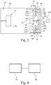
- Fig. 4 shows a flow chart illustrating steps of a method for manufacturing an X-ray source 10 according to an exemplary embodiment, wherein the X-ray source 10 may be an X-ray source 10 as described with reference to Figs. 1-3 .
- the X.-ray source 10 comprises an emitter arrangement 12 for emitting electrons or X-rays, at least one feedthrough 38 for supplying electrical power to the emitter arrangement 12, and an insulator 20 configured for isolating an electrical potential of the at least one feedthrough 38 from a ground potential.
- a first step S1 at least one cooling channel 28 is formed in an interior volume 25 of the insulator 20, such that the cooling channel 28 is completely arranged in the interior volume 25 of the insulator 20.
- the entire insulator 20 with the cooling channel 28 may be formed in a single process step, e.g. by three-dimensional printing, sintering and/or gluing of insulator sub-components, such as e.g. particles and/or granules of insulator material.
- the cooling channel 20 is formed at a distance 29 between an outer surface 26 of the insulator 20 and the cooling channel 28, which distance 29 is at least as large as half of a thickness 27 of the cooling channel 28.
- a second step S2 the insulator 20 is arranged on a side of the emitter arrangement 12, such that at least a part of the insulator 20 is in thermal contact with at least a part of the emitter arrangement 12.
Landscapes
- X-Ray Techniques (AREA)
Priority Applications (6)
| Application Number | Priority Date | Filing Date | Title |
|---|---|---|---|
| EP17176243.8A EP3416181A1 (de) | 2017-06-15 | 2017-06-15 | Röntgenstrahlquelle und verfahren zur herstellung einer röntgenstrahlquelle |
| PCT/EP2018/065790 WO2018229181A1 (en) | 2017-06-15 | 2018-06-14 | X-ray source and method for manufacturing an x-ray source |
| JP2019569331A JP2020523760A (ja) | 2017-06-15 | 2018-06-14 | X線源及びx線源の製造方法 |
| US16/621,402 US11043351B2 (en) | 2017-06-15 | 2018-06-14 | X-ray source and method for manufacturing an X-ray source |
| CN201880039644.8A CN110785827A (zh) | 2017-06-15 | 2018-06-14 | X射线源和制造x射线源的方法 |
| EP18730785.5A EP3639287A1 (de) | 2017-06-15 | 2018-06-14 | Röntgenstrahlquelle und verfahren zur herstellung einer röntgenstrahlquelle |
Applications Claiming Priority (1)
| Application Number | Priority Date | Filing Date | Title |
|---|---|---|---|
| EP17176243.8A EP3416181A1 (de) | 2017-06-15 | 2017-06-15 | Röntgenstrahlquelle und verfahren zur herstellung einer röntgenstrahlquelle |
Publications (1)
| Publication Number | Publication Date |
|---|---|
| EP3416181A1 true EP3416181A1 (de) | 2018-12-19 |
Family
ID=59067593
Family Applications (2)
| Application Number | Title | Priority Date | Filing Date |
|---|---|---|---|
| EP17176243.8A Withdrawn EP3416181A1 (de) | 2017-06-15 | 2017-06-15 | Röntgenstrahlquelle und verfahren zur herstellung einer röntgenstrahlquelle |
| EP18730785.5A Withdrawn EP3639287A1 (de) | 2017-06-15 | 2018-06-14 | Röntgenstrahlquelle und verfahren zur herstellung einer röntgenstrahlquelle |
Family Applications After (1)
| Application Number | Title | Priority Date | Filing Date |
|---|---|---|---|
| EP18730785.5A Withdrawn EP3639287A1 (de) | 2017-06-15 | 2018-06-14 | Röntgenstrahlquelle und verfahren zur herstellung einer röntgenstrahlquelle |
Country Status (5)
| Country | Link |
|---|---|
| US (1) | US11043351B2 (de) |
| EP (2) | EP3416181A1 (de) |
| JP (1) | JP2020523760A (de) |
| CN (1) | CN110785827A (de) |
| WO (1) | WO2018229181A1 (de) |
Families Citing this family (12)
| Publication number | Priority date | Publication date | Assignee | Title |
|---|---|---|---|---|
| US10295485B2 (en) | 2013-12-05 | 2019-05-21 | Sigray, Inc. | X-ray transmission spectrometer system |
| USRE48612E1 (en) | 2013-10-31 | 2021-06-29 | Sigray, Inc. | X-ray interferometric imaging system |
| US10845491B2 (en) | 2018-06-04 | 2020-11-24 | Sigray, Inc. | Energy-resolving x-ray detection system |
| GB2591630B (en) | 2018-07-26 | 2023-05-24 | Sigray Inc | High brightness x-ray reflection source |
| US10962491B2 (en) | 2018-09-04 | 2021-03-30 | Sigray, Inc. | System and method for x-ray fluorescence with filtering |
| DE112019004478T5 (de) | 2018-09-07 | 2021-07-08 | Sigray, Inc. | System und verfahren zur röntgenanalyse mit wählbarer tiefe |
| US11152183B2 (en) | 2019-07-15 | 2021-10-19 | Sigray, Inc. | X-ray source with rotating anode at atmospheric pressure |
| JP7572033B2 (ja) * | 2020-10-23 | 2024-10-23 | 株式会社リガク | 結像型x線顕微鏡 |
| CN118541772A (zh) | 2022-01-13 | 2024-08-23 | 斯格瑞公司 | 用于生成高通量低能量x射线的微焦x射线源 |
| US12360067B2 (en) | 2022-03-02 | 2025-07-15 | Sigray, Inc. | X-ray fluorescence system and x-ray source with electrically insulative target material |
| DE102022202726B4 (de) * | 2022-03-21 | 2024-02-15 | Siemens Healthcare Gmbh | Röntgenhochspannungsgenerator mit einem Zwei-Phasen-Kühlsystem |
| US12181423B1 (en) | 2023-09-07 | 2024-12-31 | Sigray, Inc. | Secondary image removal using high resolution x-ray transmission sources |
Citations (5)
| Publication number | Priority date | Publication date | Assignee | Title |
|---|---|---|---|---|
| DE674415C (de) * | 1931-03-01 | 1939-04-14 | Koch & Sterzel Akt Ges | Aus Isoliermaterial bestehendes Hochspannungsschutzgehaeuse fuer gekuehlte Vakuum-, insbesondere Roentgenroehren |
| GB1272498A (en) * | 1969-12-03 | 1972-04-26 | Philips Electronic Associated | X-ray tube having a metal envelope |
| US20040174956A1 (en) * | 2003-03-03 | 2004-09-09 | Varian Medical Systems, Inc. | Apparatus and method for shaping high voltage potentials on an insulator |
| US20100111265A1 (en) * | 2007-06-06 | 2010-05-06 | Comet Holding Ag | X-ray tube with an anode isolation element for liquid cooling and a receptacle for a high-voltage plug |
| JP2012004083A (ja) * | 2010-06-21 | 2012-01-05 | Toshiba Corp | X線管装置 |
Family Cites Families (10)
| Publication number | Priority date | Publication date | Assignee | Title |
|---|---|---|---|---|
| DE69430088T2 (de) | 1993-07-05 | 2002-11-07 | Koninklijke Philips Electronics N.V., Eindhoven | Röntgenstrahlen-Beugungsgerät mit Kühlmittel-Verbindung zur Röntgenröhre |
| US6252937B1 (en) | 1999-09-14 | 2001-06-26 | General Electric Company | High thermal performance cathode via heat pipes |
| ATE476088T1 (de) * | 2001-12-04 | 2010-08-15 | X Ray Optical Sys Inc | Röntgenquelle mit verbesserter strahlstabilität und ihre anwendung in der analyse von strömenden flüssigkeiten |
| DE102005055686B3 (de) * | 2005-11-18 | 2007-05-31 | Xtreme Technologies Gmbh | Anordnung zur Erzeugung kurzwelliger Strahlung auf Basis eines Gasentladungsplasmas sowie Verfahren zur Herstellung von kühlmitteldurchströmten Elektrodengehäusen |
| DE102006043693B4 (de) | 2006-09-18 | 2010-07-29 | Precitec Kg | Aufnahmevorrichtung mit einem ringförmigen Isolationsteil und Laserbearbeitungskopf |
| JP5322888B2 (ja) * | 2009-10-30 | 2013-10-23 | 株式会社東芝 | X線管 |
| JP2012003995A (ja) | 2010-06-18 | 2012-01-05 | Hitachi Medical Corp | X線管およびx線撮影装置 |
| JP5748205B2 (ja) * | 2010-08-27 | 2015-07-15 | ギガフォトン株式会社 | ウィンドウユニット、ウィンドウ装置、レーザ装置及び極端紫外光生成装置 |
| US20160020059A1 (en) | 2012-07-11 | 2016-01-21 | Comet Holding Ag | Cooling arrangement for x-ray generator |
| EP3612096A4 (de) * | 2017-04-17 | 2020-12-23 | Rapiscan Systems, Inc. | Röntgenstrahltomographieinspektionssysteme und -verfahren |
-
2017
- 2017-06-15 EP EP17176243.8A patent/EP3416181A1/de not_active Withdrawn
-
2018
- 2018-06-14 EP EP18730785.5A patent/EP3639287A1/de not_active Withdrawn
- 2018-06-14 WO PCT/EP2018/065790 patent/WO2018229181A1/en not_active Ceased
- 2018-06-14 US US16/621,402 patent/US11043351B2/en not_active Expired - Fee Related
- 2018-06-14 CN CN201880039644.8A patent/CN110785827A/zh active Pending
- 2018-06-14 JP JP2019569331A patent/JP2020523760A/ja active Pending
Patent Citations (5)
| Publication number | Priority date | Publication date | Assignee | Title |
|---|---|---|---|---|
| DE674415C (de) * | 1931-03-01 | 1939-04-14 | Koch & Sterzel Akt Ges | Aus Isoliermaterial bestehendes Hochspannungsschutzgehaeuse fuer gekuehlte Vakuum-, insbesondere Roentgenroehren |
| GB1272498A (en) * | 1969-12-03 | 1972-04-26 | Philips Electronic Associated | X-ray tube having a metal envelope |
| US20040174956A1 (en) * | 2003-03-03 | 2004-09-09 | Varian Medical Systems, Inc. | Apparatus and method for shaping high voltage potentials on an insulator |
| US20100111265A1 (en) * | 2007-06-06 | 2010-05-06 | Comet Holding Ag | X-ray tube with an anode isolation element for liquid cooling and a receptacle for a high-voltage plug |
| JP2012004083A (ja) * | 2010-06-21 | 2012-01-05 | Toshiba Corp | X線管装置 |
Also Published As
| Publication number | Publication date |
|---|---|
| WO2018229181A1 (en) | 2018-12-20 |
| CN110785827A (zh) | 2020-02-11 |
| EP3639287A1 (de) | 2020-04-22 |
| US20200105492A1 (en) | 2020-04-02 |
| US11043351B2 (en) | 2021-06-22 |
| JP2020523760A (ja) | 2020-08-06 |
Similar Documents
| Publication | Publication Date | Title |
|---|---|---|
| US11043351B2 (en) | X-ray source and method for manufacturing an X-ray source | |
| EP2547177B1 (de) | Strahlungserzeugungsvorrichtung und Vorrichtung zur Abbildung mittels Strahlung | |
| CN110870036B (zh) | 紧凑型电离射线生成源、包括多个源的组件以及用于生产该源的方法 | |
| JP5796990B2 (ja) | X線発生装置及びそれを用いたx線撮影装置 | |
| CN105612596B (zh) | 模块化x射线源 | |
| KR102288924B1 (ko) | 원통형 엑스선 튜브 및 그 제조 방법 | |
| US10636613B2 (en) | X-ray tube, X-ray tube device, and method of manufacturing X-ray tube device | |
| JP2020523760A5 (de) | ||
| US8792619B2 (en) | X-ray tube with semiconductor coating | |
| US9824787B2 (en) | Spark gap x-ray source | |
| US20250349489A1 (en) | X-ray generation apparatus and x-ray imaging apparatus | |
| US20250351254A1 (en) | X-ray generation apparatus and x-ray imaging apparatus | |
| CN113272931A (zh) | X射线产生管、x射线产生装置及x射线成像装置 | |
| JP7073406B2 (ja) | 小型電離放射線源 | |
| US20200194213A1 (en) | Compact source for generating ionizing radiation, assembly comprising a plurality of sources and process for producing the source | |
| JP2014149932A (ja) | 放射線発生装置及び放射線撮影システム | |
| KR20170082531A (ko) | 정전기-소산 장치 | |
| TW202533629A (zh) | X射線產生裝置及x射線攝影裝置 |
Legal Events
| Date | Code | Title | Description |
|---|---|---|---|
| PUAI | Public reference made under article 153(3) epc to a published international application that has entered the european phase |
Free format text: ORIGINAL CODE: 0009012 |
|
| AK | Designated contracting states |
Kind code of ref document: A1 Designated state(s): AL AT BE BG CH CY CZ DE DK EE ES FI FR GB GR HR HU IE IS IT LI LT LU LV MC MK MT NL NO PL PT RO RS SE SI SK SM TR |
|
| AX | Request for extension of the european patent |
Extension state: BA ME |
|
| STAA | Information on the status of an ep patent application or granted ep patent |
Free format text: STATUS: THE APPLICATION IS DEEMED TO BE WITHDRAWN |
|
| 18D | Application deemed to be withdrawn |
Effective date: 20190620 |