EP3418265A1 - Module de puissance logique à substrat exposé à pâte pour films épais lié à des feuilles en métal ou en hybrides de métal - Google Patents
Module de puissance logique à substrat exposé à pâte pour films épais lié à des feuilles en métal ou en hybrides de métal Download PDFInfo
- Publication number
- EP3418265A1 EP3418265A1 EP17177110.8A EP17177110A EP3418265A1 EP 3418265 A1 EP3418265 A1 EP 3418265A1 EP 17177110 A EP17177110 A EP 17177110A EP 3418265 A1 EP3418265 A1 EP 3418265A1
- Authority
- EP
- European Patent Office
- Prior art keywords
- thick
- logic
- paste
- ceramic substrate
- component
- Prior art date
- Legal status (The legal status is an assumption and is not a legal conclusion. Google has not performed a legal analysis and makes no representation as to the accuracy of the status listed.)
- Withdrawn
Links
Images
Classifications
-
- C—CHEMISTRY; METALLURGY
- C04—CEMENTS; CONCRETE; ARTIFICIAL STONE; CERAMICS; REFRACTORIES
- C04B—LIME, MAGNESIA; SLAG; CEMENTS; COMPOSITIONS THEREOF, e.g. MORTARS, CONCRETE OR LIKE BUILDING MATERIALS; ARTIFICIAL STONE; CERAMICS; REFRACTORIES; TREATMENT OF NATURAL STONE
- C04B37/00—Joining burned ceramic articles with other burned ceramic articles or other articles by heating
- C04B37/02—Joining burned ceramic articles with other burned ceramic articles or other articles by heating with metallic articles
- C04B37/023—Joining burned ceramic articles with other burned ceramic articles or other articles by heating with metallic articles characterised by the interlayer used
-
- C—CHEMISTRY; METALLURGY
- C04—CEMENTS; CONCRETE; ARTIFICIAL STONE; CERAMICS; REFRACTORIES
- C04B—LIME, MAGNESIA; SLAG; CEMENTS; COMPOSITIONS THEREOF, e.g. MORTARS, CONCRETE OR LIKE BUILDING MATERIALS; ARTIFICIAL STONE; CERAMICS; REFRACTORIES; TREATMENT OF NATURAL STONE
- C04B37/00—Joining burned ceramic articles with other burned ceramic articles or other articles by heating
- C04B37/02—Joining burned ceramic articles with other burned ceramic articles or other articles by heating with metallic articles
- C04B37/023—Joining burned ceramic articles with other burned ceramic articles or other articles by heating with metallic articles characterised by the interlayer used
- C04B37/026—Joining burned ceramic articles with other burned ceramic articles or other articles by heating with metallic articles characterised by the interlayer used consisting of metals or metal salts
-
- C—CHEMISTRY; METALLURGY
- C03—GLASS; MINERAL OR SLAG WOOL
- C03C—CHEMICAL COMPOSITION OF GLASSES, GLAZES OR VITREOUS ENAMELS; SURFACE TREATMENT OF GLASS; SURFACE TREATMENT OF FIBRES OR FILAMENTS MADE FROM GLASS, MINERALS OR SLAGS; JOINING GLASS TO GLASS OR OTHER MATERIALS
- C03C4/00—Compositions for glass with special properties
- C03C4/14—Compositions for glass with special properties for electro-conductive glass
-
- C—CHEMISTRY; METALLURGY
- C03—GLASS; MINERAL OR SLAG WOOL
- C03C—CHEMICAL COMPOSITION OF GLASSES, GLAZES OR VITREOUS ENAMELS; SURFACE TREATMENT OF GLASS; SURFACE TREATMENT OF FIBRES OR FILAMENTS MADE FROM GLASS, MINERALS OR SLAGS; JOINING GLASS TO GLASS OR OTHER MATERIALS
- C03C8/00—Enamels; Glazes; Fusion seal compositions being frit compositions having non-frit additions
- C03C8/02—Frit compositions, i.e. in a powdered or comminuted form
- C03C8/04—Frit compositions, i.e. in a powdered or comminuted form containing zinc
-
- C—CHEMISTRY; METALLURGY
- C03—GLASS; MINERAL OR SLAG WOOL
- C03C—CHEMICAL COMPOSITION OF GLASSES, GLAZES OR VITREOUS ENAMELS; SURFACE TREATMENT OF GLASS; SURFACE TREATMENT OF FIBRES OR FILAMENTS MADE FROM GLASS, MINERALS OR SLAGS; JOINING GLASS TO GLASS OR OTHER MATERIALS
- C03C8/00—Enamels; Glazes; Fusion seal compositions being frit compositions having non-frit additions
- C03C8/24—Fusion seal compositions being frit compositions having non-frit additions, i.e. for use as seals between dissimilar materials, e.g. glass and metal; Glass solders
-
- H—ELECTRICITY
- H05—ELECTRIC TECHNIQUES NOT OTHERWISE PROVIDED FOR
- H05K—PRINTED CIRCUITS; CASINGS OR CONSTRUCTIONAL DETAILS OF ELECTRIC APPARATUS; MANUFACTURE OF ASSEMBLAGES OF ELECTRICAL COMPONENTS
- H05K1/00—Printed circuits
- H05K1/02—Details
- H05K1/03—Use of materials for the substrate
- H05K1/0306—Inorganic insulating substrates, e.g. ceramic, glass
-
- H—ELECTRICITY
- H05—ELECTRIC TECHNIQUES NOT OTHERWISE PROVIDED FOR
- H05K—PRINTED CIRCUITS; CASINGS OR CONSTRUCTIONAL DETAILS OF ELECTRIC APPARATUS; MANUFACTURE OF ASSEMBLAGES OF ELECTRICAL COMPONENTS
- H05K3/00—Apparatus or processes for manufacturing printed circuits
- H05K3/10—Apparatus or processes for manufacturing printed circuits in which conductive material is applied to the insulating support in such a manner as to form the desired conductive pattern
- H05K3/12—Apparatus or processes for manufacturing printed circuits in which conductive material is applied to the insulating support in such a manner as to form the desired conductive pattern using thick film techniques, e.g. printing techniques to apply the conductive material or similar techniques for applying conductive paste or ink patterns
- H05K3/1216—Apparatus or processes for manufacturing printed circuits in which conductive material is applied to the insulating support in such a manner as to form the desired conductive pattern using thick film techniques, e.g. printing techniques to apply the conductive material or similar techniques for applying conductive paste or ink patterns by screen printing or stencil printing
-
- H—ELECTRICITY
- H10—SEMICONDUCTOR DEVICES; ELECTRIC SOLID-STATE DEVICES NOT OTHERWISE PROVIDED FOR
- H10W—GENERIC PACKAGES, INTERCONNECTIONS, CONNECTORS OR OTHER CONSTRUCTIONAL DETAILS OF DEVICES COVERED BY CLASS H10
- H10W70/00—Package substrates; Interposers; Redistribution layers [RDL]
- H10W70/01—Manufacture or treatment
- H10W70/05—Manufacture or treatment of insulating or insulated package substrates, or of interposers, or of redistribution layers
-
- H—ELECTRICITY
- H10—SEMICONDUCTOR DEVICES; ELECTRIC SOLID-STATE DEVICES NOT OTHERWISE PROVIDED FOR
- H10W—GENERIC PACKAGES, INTERCONNECTIONS, CONNECTORS OR OTHER CONSTRUCTIONAL DETAILS OF DEVICES COVERED BY CLASS H10
- H10W70/00—Package substrates; Interposers; Redistribution layers [RDL]
- H10W70/60—Insulating or insulated package substrates; Interposers; Redistribution layers
- H10W70/67—Insulating or insulated package substrates; Interposers; Redistribution layers characterised by their insulating layers or insulating parts
- H10W70/69—Insulating materials thereof
- H10W70/692—Ceramics or glasses
-
- H—ELECTRICITY
- H10—SEMICONDUCTOR DEVICES; ELECTRIC SOLID-STATE DEVICES NOT OTHERWISE PROVIDED FOR
- H10W—GENERIC PACKAGES, INTERCONNECTIONS, CONNECTORS OR OTHER CONSTRUCTIONAL DETAILS OF DEVICES COVERED BY CLASS H10
- H10W90/00—Package configurations
-
- C—CHEMISTRY; METALLURGY
- C03—GLASS; MINERAL OR SLAG WOOL
- C03C—CHEMICAL COMPOSITION OF GLASSES, GLAZES OR VITREOUS ENAMELS; SURFACE TREATMENT OF GLASS; SURFACE TREATMENT OF FIBRES OR FILAMENTS MADE FROM GLASS, MINERALS OR SLAGS; JOINING GLASS TO GLASS OR OTHER MATERIALS
- C03C2204/00—Glasses, glazes or enamels with special properties
-
- C—CHEMISTRY; METALLURGY
- C03—GLASS; MINERAL OR SLAG WOOL
- C03C—CHEMICAL COMPOSITION OF GLASSES, GLAZES OR VITREOUS ENAMELS; SURFACE TREATMENT OF GLASS; SURFACE TREATMENT OF FIBRES OR FILAMENTS MADE FROM GLASS, MINERALS OR SLAGS; JOINING GLASS TO GLASS OR OTHER MATERIALS
- C03C2205/00—Compositions applicable for the manufacture of vitreous enamels or glazes
-
- C—CHEMISTRY; METALLURGY
- C04—CEMENTS; CONCRETE; ARTIFICIAL STONE; CERAMICS; REFRACTORIES
- C04B—LIME, MAGNESIA; SLAG; CEMENTS; COMPOSITIONS THEREOF, e.g. MORTARS, CONCRETE OR LIKE BUILDING MATERIALS; ARTIFICIAL STONE; CERAMICS; REFRACTORIES; TREATMENT OF NATURAL STONE
- C04B2237/00—Aspects relating to ceramic laminates or to joining of ceramic articles with other articles by heating
- C04B2237/02—Aspects relating to interlayers, e.g. used to join ceramic articles with other articles by heating
- C04B2237/10—Glass interlayers, e.g. frit or flux
-
- C—CHEMISTRY; METALLURGY
- C04—CEMENTS; CONCRETE; ARTIFICIAL STONE; CERAMICS; REFRACTORIES
- C04B—LIME, MAGNESIA; SLAG; CEMENTS; COMPOSITIONS THEREOF, e.g. MORTARS, CONCRETE OR LIKE BUILDING MATERIALS; ARTIFICIAL STONE; CERAMICS; REFRACTORIES; TREATMENT OF NATURAL STONE
- C04B2237/00—Aspects relating to ceramic laminates or to joining of ceramic articles with other articles by heating
- C04B2237/02—Aspects relating to interlayers, e.g. used to join ceramic articles with other articles by heating
- C04B2237/12—Metallic interlayers
- C04B2237/124—Metallic interlayers based on copper
-
- C—CHEMISTRY; METALLURGY
- C04—CEMENTS; CONCRETE; ARTIFICIAL STONE; CERAMICS; REFRACTORIES
- C04B—LIME, MAGNESIA; SLAG; CEMENTS; COMPOSITIONS THEREOF, e.g. MORTARS, CONCRETE OR LIKE BUILDING MATERIALS; ARTIFICIAL STONE; CERAMICS; REFRACTORIES; TREATMENT OF NATURAL STONE
- C04B2237/00—Aspects relating to ceramic laminates or to joining of ceramic articles with other articles by heating
- C04B2237/30—Composition of layers of ceramic laminates or of ceramic or metallic articles to be joined by heating, e.g. Si substrates
- C04B2237/32—Ceramic
-
- C—CHEMISTRY; METALLURGY
- C04—CEMENTS; CONCRETE; ARTIFICIAL STONE; CERAMICS; REFRACTORIES
- C04B—LIME, MAGNESIA; SLAG; CEMENTS; COMPOSITIONS THEREOF, e.g. MORTARS, CONCRETE OR LIKE BUILDING MATERIALS; ARTIFICIAL STONE; CERAMICS; REFRACTORIES; TREATMENT OF NATURAL STONE
- C04B2237/00—Aspects relating to ceramic laminates or to joining of ceramic articles with other articles by heating
- C04B2237/30—Composition of layers of ceramic laminates or of ceramic or metallic articles to be joined by heating, e.g. Si substrates
- C04B2237/32—Ceramic
- C04B2237/34—Oxidic
- C04B2237/343—Alumina or aluminates
-
- C—CHEMISTRY; METALLURGY
- C04—CEMENTS; CONCRETE; ARTIFICIAL STONE; CERAMICS; REFRACTORIES
- C04B—LIME, MAGNESIA; SLAG; CEMENTS; COMPOSITIONS THEREOF, e.g. MORTARS, CONCRETE OR LIKE BUILDING MATERIALS; ARTIFICIAL STONE; CERAMICS; REFRACTORIES; TREATMENT OF NATURAL STONE
- C04B2237/00—Aspects relating to ceramic laminates or to joining of ceramic articles with other articles by heating
- C04B2237/30—Composition of layers of ceramic laminates or of ceramic or metallic articles to be joined by heating, e.g. Si substrates
- C04B2237/32—Ceramic
- C04B2237/36—Non-oxidic
- C04B2237/366—Aluminium nitride
-
- C—CHEMISTRY; METALLURGY
- C04—CEMENTS; CONCRETE; ARTIFICIAL STONE; CERAMICS; REFRACTORIES
- C04B—LIME, MAGNESIA; SLAG; CEMENTS; COMPOSITIONS THEREOF, e.g. MORTARS, CONCRETE OR LIKE BUILDING MATERIALS; ARTIFICIAL STONE; CERAMICS; REFRACTORIES; TREATMENT OF NATURAL STONE
- C04B2237/00—Aspects relating to ceramic laminates or to joining of ceramic articles with other articles by heating
- C04B2237/30—Composition of layers of ceramic laminates or of ceramic or metallic articles to be joined by heating, e.g. Si substrates
- C04B2237/32—Ceramic
- C04B2237/36—Non-oxidic
- C04B2237/368—Silicon nitride
-
- C—CHEMISTRY; METALLURGY
- C04—CEMENTS; CONCRETE; ARTIFICIAL STONE; CERAMICS; REFRACTORIES
- C04B—LIME, MAGNESIA; SLAG; CEMENTS; COMPOSITIONS THEREOF, e.g. MORTARS, CONCRETE OR LIKE BUILDING MATERIALS; ARTIFICIAL STONE; CERAMICS; REFRACTORIES; TREATMENT OF NATURAL STONE
- C04B2237/00—Aspects relating to ceramic laminates or to joining of ceramic articles with other articles by heating
- C04B2237/30—Composition of layers of ceramic laminates or of ceramic or metallic articles to be joined by heating, e.g. Si substrates
- C04B2237/40—Metallic
-
- C—CHEMISTRY; METALLURGY
- C04—CEMENTS; CONCRETE; ARTIFICIAL STONE; CERAMICS; REFRACTORIES
- C04B—LIME, MAGNESIA; SLAG; CEMENTS; COMPOSITIONS THEREOF, e.g. MORTARS, CONCRETE OR LIKE BUILDING MATERIALS; ARTIFICIAL STONE; CERAMICS; REFRACTORIES; TREATMENT OF NATURAL STONE
- C04B2237/00—Aspects relating to ceramic laminates or to joining of ceramic articles with other articles by heating
- C04B2237/30—Composition of layers of ceramic laminates or of ceramic or metallic articles to be joined by heating, e.g. Si substrates
- C04B2237/40—Metallic
- C04B2237/407—Copper
-
- C—CHEMISTRY; METALLURGY
- C04—CEMENTS; CONCRETE; ARTIFICIAL STONE; CERAMICS; REFRACTORIES
- C04B—LIME, MAGNESIA; SLAG; CEMENTS; COMPOSITIONS THEREOF, e.g. MORTARS, CONCRETE OR LIKE BUILDING MATERIALS; ARTIFICIAL STONE; CERAMICS; REFRACTORIES; TREATMENT OF NATURAL STONE
- C04B2237/00—Aspects relating to ceramic laminates or to joining of ceramic articles with other articles by heating
- C04B2237/50—Processing aspects relating to ceramic laminates or to the joining of ceramic articles with other articles by heating
- C04B2237/54—Oxidising the surface before joining
-
- C—CHEMISTRY; METALLURGY
- C04—CEMENTS; CONCRETE; ARTIFICIAL STONE; CERAMICS; REFRACTORIES
- C04B—LIME, MAGNESIA; SLAG; CEMENTS; COMPOSITIONS THEREOF, e.g. MORTARS, CONCRETE OR LIKE BUILDING MATERIALS; ARTIFICIAL STONE; CERAMICS; REFRACTORIES; TREATMENT OF NATURAL STONE
- C04B2237/00—Aspects relating to ceramic laminates or to joining of ceramic articles with other articles by heating
- C04B2237/50—Processing aspects relating to ceramic laminates or to the joining of ceramic articles with other articles by heating
- C04B2237/59—Aspects relating to the structure of the interlayer
- C04B2237/592—Aspects relating to the structure of the interlayer whereby the interlayer is not continuous, e.g. not the whole surface of the smallest substrate is covered by the interlayer
-
- C—CHEMISTRY; METALLURGY
- C04—CEMENTS; CONCRETE; ARTIFICIAL STONE; CERAMICS; REFRACTORIES
- C04B—LIME, MAGNESIA; SLAG; CEMENTS; COMPOSITIONS THEREOF, e.g. MORTARS, CONCRETE OR LIKE BUILDING MATERIALS; ARTIFICIAL STONE; CERAMICS; REFRACTORIES; TREATMENT OF NATURAL STONE
- C04B2237/00—Aspects relating to ceramic laminates or to joining of ceramic articles with other articles by heating
- C04B2237/50—Processing aspects relating to ceramic laminates or to the joining of ceramic articles with other articles by heating
- C04B2237/59—Aspects relating to the structure of the interlayer
- C04B2237/595—Aspects relating to the structure of the interlayer whereby the interlayer is continuous, but heterogeneous on macro-scale, e.g. one part of the interlayer being a joining material, another part being an electrode material
-
- H—ELECTRICITY
- H05—ELECTRIC TECHNIQUES NOT OTHERWISE PROVIDED FOR
- H05K—PRINTED CIRCUITS; CASINGS OR CONSTRUCTIONAL DETAILS OF ELECTRIC APPARATUS; MANUFACTURE OF ASSEMBLAGES OF ELECTRICAL COMPONENTS
- H05K2201/00—Indexing scheme relating to printed circuits covered by H05K1/00
- H05K2201/03—Conductive materials
- H05K2201/0332—Structure of the conductor
- H05K2201/0335—Layered conductors or foils
- H05K2201/0355—Metal foils
-
- H—ELECTRICITY
- H05—ELECTRIC TECHNIQUES NOT OTHERWISE PROVIDED FOR
- H05K—PRINTED CIRCUITS; CASINGS OR CONSTRUCTIONAL DETAILS OF ELECTRIC APPARATUS; MANUFACTURE OF ASSEMBLAGES OF ELECTRICAL COMPONENTS
- H05K2203/00—Indexing scheme relating to apparatus or processes for manufacturing printed circuits covered by H05K3/00
- H05K2203/11—Treatments characterised by their effect, e.g. heating, cooling, roughening
- H05K2203/1126—Firing, i.e. heating a powder or paste above the melting temperature of at least one of its constituents
-
- H—ELECTRICITY
- H05—ELECTRIC TECHNIQUES NOT OTHERWISE PROVIDED FOR
- H05K—PRINTED CIRCUITS; CASINGS OR CONSTRUCTIONAL DETAILS OF ELECTRIC APPARATUS; MANUFACTURE OF ASSEMBLAGES OF ELECTRICAL COMPONENTS
- H05K3/00—Apparatus or processes for manufacturing printed circuits
- H05K3/38—Improvement of the adhesion between the insulating substrate and the metal
- H05K3/382—Improvement of the adhesion between the insulating substrate and the metal by special treatment of the metal
- H05K3/385—Improvement of the adhesion between the insulating substrate and the metal by special treatment of the metal by conversion of the surface of the metal, e.g. by oxidation, whether or not followed by reaction or removal of the converted layer
-
- H—ELECTRICITY
- H10—SEMICONDUCTOR DEVICES; ELECTRIC SOLID-STATE DEVICES NOT OTHERWISE PROVIDED FOR
- H10W—GENERIC PACKAGES, INTERCONNECTIONS, CONNECTORS OR OTHER CONSTRUCTIONAL DETAILS OF DEVICES COVERED BY CLASS H10
- H10W72/00—Interconnections or connectors in packages
- H10W72/01—Manufacture or treatment
- H10W72/013—Manufacture or treatment of die-attach connectors
-
- H—ELECTRICITY
- H10—SEMICONDUCTOR DEVICES; ELECTRIC SOLID-STATE DEVICES NOT OTHERWISE PROVIDED FOR
- H10W—GENERIC PACKAGES, INTERCONNECTIONS, CONNECTORS OR OTHER CONSTRUCTIONAL DETAILS OF DEVICES COVERED BY CLASS H10
- H10W72/00—Interconnections or connectors in packages
- H10W72/01—Manufacture or treatment
- H10W72/013—Manufacture or treatment of die-attach connectors
- H10W72/01321—Manufacture or treatment of die-attach connectors using local deposition
- H10W72/01323—Manufacture or treatment of die-attach connectors using local deposition in liquid form, e.g. by dispensing droplets or by screen printing
-
- H—ELECTRICITY
- H10—SEMICONDUCTOR DEVICES; ELECTRIC SOLID-STATE DEVICES NOT OTHERWISE PROVIDED FOR
- H10W—GENERIC PACKAGES, INTERCONNECTIONS, CONNECTORS OR OTHER CONSTRUCTIONAL DETAILS OF DEVICES COVERED BY CLASS H10
- H10W72/00—Interconnections or connectors in packages
- H10W72/071—Connecting or disconnecting
- H10W72/073—Connecting or disconnecting of die-attach connectors
-
- H—ELECTRICITY
- H10—SEMICONDUCTOR DEVICES; ELECTRIC SOLID-STATE DEVICES NOT OTHERWISE PROVIDED FOR
- H10W—GENERIC PACKAGES, INTERCONNECTIONS, CONNECTORS OR OTHER CONSTRUCTIONAL DETAILS OF DEVICES COVERED BY CLASS H10
- H10W72/00—Interconnections or connectors in packages
- H10W72/071—Connecting or disconnecting
- H10W72/073—Connecting or disconnecting of die-attach connectors
- H10W72/07331—Connecting techniques
-
- H—ELECTRICITY
- H10—SEMICONDUCTOR DEVICES; ELECTRIC SOLID-STATE DEVICES NOT OTHERWISE PROVIDED FOR
- H10W—GENERIC PACKAGES, INTERCONNECTIONS, CONNECTORS OR OTHER CONSTRUCTIONAL DETAILS OF DEVICES COVERED BY CLASS H10
- H10W72/00—Interconnections or connectors in packages
- H10W72/071—Connecting or disconnecting
- H10W72/073—Connecting or disconnecting of die-attach connectors
- H10W72/07341—Controlling the bonding environment, e.g. atmosphere composition or temperature
-
- H—ELECTRICITY
- H10—SEMICONDUCTOR DEVICES; ELECTRIC SOLID-STATE DEVICES NOT OTHERWISE PROVIDED FOR
- H10W—GENERIC PACKAGES, INTERCONNECTIONS, CONNECTORS OR OTHER CONSTRUCTIONAL DETAILS OF DEVICES COVERED BY CLASS H10
- H10W72/00—Interconnections or connectors in packages
- H10W72/30—Die-attach connectors
- H10W72/321—Structures or relative sizes of die-attach connectors
- H10W72/325—Die-attach connectors having a filler embedded in a matrix
-
- H—ELECTRICITY
- H10—SEMICONDUCTOR DEVICES; ELECTRIC SOLID-STATE DEVICES NOT OTHERWISE PROVIDED FOR
- H10W—GENERIC PACKAGES, INTERCONNECTIONS, CONNECTORS OR OTHER CONSTRUCTIONAL DETAILS OF DEVICES COVERED BY CLASS H10
- H10W72/00—Interconnections or connectors in packages
- H10W72/30—Die-attach connectors
- H10W72/351—Materials of die-attach connectors
- H10W72/352—Materials of die-attach connectors comprising metals or metalloids, e.g. solders
-
- H—ELECTRICITY
- H10—SEMICONDUCTOR DEVICES; ELECTRIC SOLID-STATE DEVICES NOT OTHERWISE PROVIDED FOR
- H10W—GENERIC PACKAGES, INTERCONNECTIONS, CONNECTORS OR OTHER CONSTRUCTIONAL DETAILS OF DEVICES COVERED BY CLASS H10
- H10W72/00—Interconnections or connectors in packages
- H10W72/30—Die-attach connectors
- H10W72/351—Materials of die-attach connectors
- H10W72/353—Materials of die-attach connectors not comprising solid metals or solid metalloids, e.g. ceramics
-
- H—ELECTRICITY
- H10—SEMICONDUCTOR DEVICES; ELECTRIC SOLID-STATE DEVICES NOT OTHERWISE PROVIDED FOR
- H10W—GENERIC PACKAGES, INTERCONNECTIONS, CONNECTORS OR OTHER CONSTRUCTIONAL DETAILS OF DEVICES COVERED BY CLASS H10
- H10W72/00—Interconnections or connectors in packages
- H10W72/30—Die-attach connectors
- H10W72/351—Materials of die-attach connectors
- H10W72/353—Materials of die-attach connectors not comprising solid metals or solid metalloids, e.g. ceramics
- H10W72/354—Materials of die-attach connectors not comprising solid metals or solid metalloids, e.g. ceramics comprising polymers
-
- H—ELECTRICITY
- H10—SEMICONDUCTOR DEVICES; ELECTRIC SOLID-STATE DEVICES NOT OTHERWISE PROVIDED FOR
- H10W—GENERIC PACKAGES, INTERCONNECTIONS, CONNECTORS OR OTHER CONSTRUCTIONAL DETAILS OF DEVICES COVERED BY CLASS H10
- H10W90/00—Package configurations
- H10W90/701—Package configurations characterised by the relative positions of pads or connectors relative to package parts
- H10W90/731—Package configurations characterised by the relative positions of pads or connectors relative to package parts of die-attach connectors
- H10W90/734—Package configurations characterised by the relative positions of pads or connectors relative to package parts of die-attach connectors between a chip and a stacked insulating package substrate, interposer or RDL
Definitions
- the present invention relates to a logic power module, comprising at least one logic component, at least one power component and a substrate, whereby the logic component and the power component are provided in separate areas on the substrate.
- the present invention relates to a process for the preparation of said logic power module and to the use of said logic power module.
- Logic power modules can be built as completely independent parts, the power modules usually made on a DCB-Al 2 O 3 substrate (Direct Copper Bonding), on a DCB-AIN-substrate, on a DCB-Si 3 N 4 -substrate or on an IMS-substrate (insulated metal substrate) and the logic modules are manufactured on epoxy PCB or by using thick film techniques.
- a DCB-Al 2 O 3 substrate Direct Copper Bonding
- DCB-AIN-substrate on a DCB-Si 3 N 4 -substrate or on an IMS-substrate (insulated metal substrate)
- IMS-substrate insulated metal substrate
- the logic modules are manufactured on epoxy PCB or by using thick film techniques.
- thick film technology many possible different thicknesses of the logic modules can be prepared. In some cases thick logic modules in the range of about 300 ⁇ m thickness and slightly thinner logic modules in the range of about 10 ⁇ m thickness can be prepared on the same substrate.
- the thick film technique allows to
- DCB Direct copper bonded
- substrates are commonly used in power modules because of their very good thermal conductivity. They are composed of a ceramic tile (commonly alumina) with a sheet of copper bonded to one or both sides by a high-temperature oxidation process (the copper and substrate are heated to a carefully controlled temperature in an atmosphere of nitrogen containing about 30 ppm of oxygen; under these conditions, a copper-oxygen eutectic forms which bonds successfully both to copper and the oxides used as substrates).
- the top copper layer can be preformed prior to firing or chemically etched using printed circuit board technology to form an electrical circuit, while the bottom copper layer is usually kept plain.
- the substrate is attached to a heat spreader by soldering the bottom copper layer to it.
- a copper foil is bonded onto a ceramic substrate with a eutectic melt.
- This process technology suffers from some disadvantages, such as a high amount of rejects, the creation of cavities between the ceramic substrate and the copper foil and the relatively low resistance against temperature changes (which leads to a delamination after some thermic cycles).
- a respective technology is described, for example, in DE 10 2010 025 313 A in which a mixture of the metal and an oxide of this metal is applied on a ceramic substrate which is then bonded via a DCB process.
- substrates which are prepared based on the thick print technology, are also known.
- the unpublished prior patent application PCT/EP2016/082161 propose a metal ceramic substrate which is prepared by applying of a thick-film paste onto a ceramic substrate; applying of a metal foil onto the thick-film layer of the ceramic substrate; and bonding of the metal foil with the ceramic substrate via the thick-film layer.
- This metal ceramic substrate exhibits an improved stability (i.e., a reduced risk of delamination), a high conductivity and a high durability and can be produced with reduced costs.
- the unpublished prior patent application PCT/EP2016/082161 does not disclose the use of the underlying technology in the field of logic power modules.
- the present invention now provides a further application of the technology underlying PCT/EP2016/082161 and provides logic power modules that comprises a logic component and a power component on one substrate, whereby the power component is prepared by the modified DCB technology as described in the unpublished prior patent application PCT/EP2016/082161 .
- the present invention relates to a logic power module, comprising at least one logic component, at least one power component and a substrate, whereby the logic element and the power component are provided in separate areas on the substrate.
- the logic component relates to the part of the power logic module which comprises, inter alia, conductors for digital and analog signals, die attach structures (on, for example, chips are provided), and passive electronic components, such as resistors, capacitors etc.
- thick-printed metal means in particular thick-printed copper and thick-printed silver, whereby thick-printed copper is preferred.
- the present invention allows to print the thick metal layer of the logic component and the metal-containing thick film layer of the power component in one process step (i.e., at the same time) which facilitates the production of the logic power module according to the present invention.
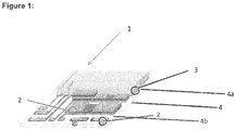
- reference number 1 stands for the logic power module
- reference number 2 stands for the logic component
- reference number 3 stands for the power component
- reference number 4 stands for the substrate, on which the area of the logic component is designated with the reference number 4a, while the area of the power component is designated with the reference number 4b.
- the logic power module 1 comprises one logic component 2 and at least one power component 3 on the same ceramic substrate.
- the logic component 2 and the power component 3 are described in more detail.
- the logic component 2 of the logic power module according to the present invention may be prepared by an electroconductive paste, preferably a copper paste, which is deposited, dried and sintered, preferably by firing.
- the process of firing can be carried out in a protective atmosphere, such as a nitrogen atmosphere or argon atmosphere.
- the thick printed metal paste can be provided on the ceramic substrate by a single printing step or by several printing steps, whereby in case of several printing steps the same thick film metal paste or different thick printed metal pastes can be used.
- conductive layers can be connected electrically to each other by so-called vias.
- a single thick film metal paste is used in one or several printing steps.
- the logic component can be provided by different thick printed metal pastes, which are provided by individual printing steps.
- the electroconductive metal paste preferably copper paste
- the base layer composition is typically applied directly onto the substrate, and provides optimal adhesion to the ceramic substrate.
- the top layer composition is typically applied over a fired base layer composition layer or another fired top layer composition layer. Multiple layers of the top layer composition may be applied in order to build the metal conductor, preferably copper conductor, to a desired thickness on the substrate in the logic area.
- a base layer electroconductive metal paste composition preferably a copper paste composition
- a base layer electroconductive metal paste composition may be first deposited on the ceramic substrate, dried and sintered, preferably fired.
- Subsequent layer(s) of top layer electroconductive metal paste composition preferably copper paste composition. may be deposited on the fired base layer or previously fired top layer to build up the metal conductor to a desired thickness.
- the base layer electroconductive metal paste preferably electroconductive copper paste
- the ceramic substrate dried and subsequent layer(s) of metal paste, preferably copper paste, are printed thereon without prior sintering, preferably firing, of the underlying paste layer(s).
- Each layer may be dried before printing the subsequent layer.
- the layers may be sintered, preferably fired, in a final step to form the metal conductor(s) in the desired thickness.
- the electroconductive metal paste compositions preferably the copper paste compositions. may be applied to the ceramic substrate via screen printing, stencil printing, direct deposition, or any other means known to one skilled in the art.
- the preferred application method is screen printing.
- a stainless steel mesh screen with an emulsion layer comprising the predetermined circuitry is employed for the screen printing process.
- the printed electroconductive metal paste compositions are typically dried at a moderate temperature to prevent the oxidation of the metal particles.
- the drying temperature is about 100 to 130 °C, preferably 125 °C, and the drying time is about 5 to 15 min.
- the firing of the electroconductive metal paste compositions, preferably copper paste compositions, and ceramic substrate are typically conducted in a furnace at about 850 to 1050 °C, preferably 925 to 950 °C, peak temperature in a low oxygen atmosphere, such as a nitrogen atmosphere with an O 2 content typically below 10 to 20 ppm, preferably about 1 to 3 ppm, O 2 .
- a low oxygen atmosphere such as a nitrogen atmosphere with an O 2 content typically below 10 to 20 ppm, preferably about 1 to 3 ppm, O 2 .
- the dwelling time at peak firing temperature is about 5 to 10 min, preferably 8 to 10 min.
- the logic component may be prepared on a ceramic substrate using the electroconductive metal pastes, preferably the copper pastes, by a process comprising:
- the process defined above can further comprise a or more step(s) of depositing further electroconductive layer(s), in particular copper layer(s), and/or a dielectric layer(s).
- the metal conductor in the logic component may be built to the desired thickness by repeating the steps (iv) to (vi).
- the fired thickness of the metal conductor is about 10 to 75 ⁇ m, preferably 15 to 50 ⁇ m, for each layer of electroconductive metal paste.
- steps (iv) to (vi) may be repeated 1 to 10 times.
- a metal conductor in the logic component of a fired thickness of about 300 ⁇ m can be achieved with one layer of base layer paste and up to ten layers of top layer paste.
- the electroconductive paste composition used for the logic component may comprise a glass frit, whereby the base layer electroconductive paste composition may comprise a higher amount of glass frit than the top layer electroconductive paste composition.
- the base layer electroconductive paste comprises from about 1 to about 5 wt. % of glass frit.
- the top layer electroconductive paste comprises preferably of from 0 to 20 wt.-%, more preferably 0 to 5 wt.-%,of glass frit.
- the electroconductive paste composition used for the logic component may also comprise no glass frit.
- the electroconductive paste composition used for the logic component comprises usually an adhesion promoter, whereby the base layer may comprise a higher amount of adhesion promoter than the top layer electroconductive paste composition.
- the base layer electroconductive paste comprises from about 1 to about 5 wt. % of adhesion promoter, preferably from about 2 to about 4 wt. %, more preferably about 3 wt. % of adhesion promoter.
- the top layer electroconductive paste comprises from about 0.25 to about 1.25 wt. % of adhesion promoter, preferably from about 0.75 to about 1.25 wt. %, more preferably about 1 wt. % of adhesion promoter.
- the thick-film paste used for the logic component may comprise copper as a metal and optionally Bi 2 O 3 .
- the electroconductive paste comprises preferably 40 to 92 wt.-% copper, more preferably 40 to less than 92 wt.-% copper, more preferably 70 to less than 92 wt.-% copper, most preferably 75 to 90 wt.-% copper, each based on the total weight of the electroconductive paste.
- the electroconductive paste comprises preferably 0 to 50 wt.-% Bi 2 O 3 , more preferably 1 to 20 wt.-% Bi 2 O 3 , most preferably 2 to 15 wt.-% Bi 2 O 3 , each based on the total weight of the electroconductive.
- the copper particles used in the electroconductive paste have a median diameter (d 50 ) preferably of between 0.1 to 20 ⁇ m, more preferably of between 1 and 10 ⁇ m, most preferably of between 2 and 7 ⁇ m.
- the Bi 2 O 3 particles used optionally in the electroconductive paste have a median diameter (d 50 ) preferably of less than 100 ⁇ m, more preferably of less than 20 ⁇ m, most preferably of less than 10 ⁇ m.
- the electroconductive paste may comprise copper and a glass component as already mentioned above.
- the amount of copper in the electroconductive paste in case of a simultaneous use of a glass component might be as defined above, i.e. preferably in an amount of from 40 to 92 wt.-%, more preferably 40 to less than 92 wt.-% copper, more preferably in an amount of from 70 to less than 92 wt.-% copper, most preferably in an amount of from 75 to 90 wt.-% copper, each based on the total weight of the electroconductive paste.
- the electroconductive paste comprises preferably of from 0 to 20 wt.-%, more preferably 0 to 5 wt.-%, of the glass component, each based on the total weight of the thick-film paste.
- the copper particles may have the same median diameter (d 50 ) as already mentioned above, i.e. preferably of between 0.1 to 20 ⁇ m, more preferably of between 1 and 10 ⁇ m, most preferably of between 2 and 7 ⁇ m.
- the glass component particles may have a median diameter (d 50 ) of less than 100 ⁇ m, more preferably less than 20 ⁇ m, most preferably less than 10 ⁇ m.
- the electroconductive paste may comprise - besides the glass component and Bi 2 O 3 - further components, selected from the group consisting of PbO, TeO 2 , Bi 2 O 3 , ZnO, B 2 O 3 , Al 2 O 3 , TiO 2 , CaO, K 2 O, MgO, Na 2 O, ZrO 2 , Cu 2 O, CuO and Li 2 O.
- the assembly is fired in an inert (e.g., nitrogen) atmosphere according to a specific profile. If a metal conductive paste, preferably a copper conductive paste, is fired in an environment too rich in oxygen, the metal component may begin to oxidize.
- a minimum level of oxygen is required to facilitate burnout of the organic binder in the paste. Therefore, the level of oxygen must be optimized. According to a preferred embodiment of the invention, approximately 1 to 20 ppm of oxygen is present in the furnace atmosphere. More preferably, approximately 1 to 10 ppm of oxygen is present in the furnace atmosphere, and most preferably, approximately 1 to 3 ppm of oxygen is present.
- Preferred electroconductive paste composition are commercially available from Heraeus (thick film conductor systems, e.g. C7403 and C7404 series).
- the power component 3 is provided on the ceramic substrate of the logic power module 1 by a metal-containing thick-film layer, and, provided thereon, a metal foil.
- This power component 3 can be prepared, in a first aspect, by the following process steps:
- the structure of the power component 3 comprises
- the present invention it has been found out that based on the thick-film technology it is possible to provide a substrate for use in the field of power electronics in which a metal foil is bonded via a thick-film paste of a metal onto a ceramic substrate (such as Al 2 O 3 ceramic, AIN ceramic or Si 3 N 4 ceramic).
- a ceramic substrate such as Al 2 O 3 ceramic, AIN ceramic or Si 3 N 4 ceramic.
- the thick-film paste is applied onto the ceramic substrate in the area 4b of the ceramic substrate 4 where the resulting logic power module 1 has to to comprise the power component 3 in the first process step.
- the thick-film paste can be applied onto the ceramic substrate 4 discontinuously such that the thick-film paste is only applied on those parts of the ceramic substrate 3, which correspond to an intended electronic circuit of the final metal-ceramic substrate.
- the metal foil may be applied, thereafter, continuously over the whole thick-film layer of the ceramic substrate 4 in the area of the power component 4b. After that, the metal foil is bonded with the ceramic substrate and then structured, for example by etching.
- the metal foil may also be applied discontinuously over the thick-film layer only on those parts of the ceramic substrate on which the thick-film paste is applied.
- the thick-film paste is applied continuously onto the ceramic substrate 4 in the area of the power component 4b.
- the metal foil may be applied continuously over the whole thick-film layer of the ceramic substrate 4 in the area of the power component 4b and the metal foil and the thick-film layer are structured, for example, by etching after bonding.
- the metal foil may also be applied discontinuously only on those parts of the ceramic substrate 4 in the area of the power component 4b which correspond to an intended electronic circuit of the final logic power module 1.
- the thick-film layer is structured, for example, by etching after bonding.
- the thick-film paste may be air-dried prior to applying the metal foil onto the thick-film layer.
- the thick-film paste may also be sintered prior to applying the metal foil.
- a sintering process can be carried out by a temperature of below 1025 °C.
- the sintering process is carried out by a temperature in the range of from 300 to 1025 °C, more preferably in the range of from 600 to 1025 °C, more preferably in the range of from 900 to 1025 °C, more preferably in the range of from 900 to less than 1025 °C, more preferably in the range of from 900 to 1000 °C.
- Sintering / firing the electroconductive paste removes organic components from the wet film and ensures a good bonding of the thick film copper to the substrate.
- adhesion of the fired electroconductive film is established well below the Cu-O eutectic melting temperature. Bonding of bulk Cu foils to this fired electroconductive film is then carried out by a pure metal to metal sintering process. Accordingly, this process differs from the one described e.g in DE 10 2010 025 313 A .
- the thick-film paste may also be air-dried and sintered prior to applying the metal foil onto the thick-film layer.
- the sintering conditions are as described above.
- the sintering process of the applied thick-film paste is usually carried out under an inert atmosphere, such as a nitrogen atmosphere.
- the modified claimed process comprises the following process steps:
- the thick-film paste may be coated onto the metal foil substrate by screen printing.
- the thick-film paste may be air-dried prior to applying the metal foil onto the ceramic in the area 4b of the power component 3.
- the metal foil and the thick-film paste are structured by etching before or after bonding the metal foil onto the ceramic substrate via the thick-film layer.
- the bonding steps (1.3) and/or (2.3) are carried out by firing.
- the firing is carried out at a temperature of between 750 and 1100 °C, more preferably of between 800 and 1085 °C, even more preferably of between 900 and 1085 °C.
- the metal foil is bonded via the thick-film paste to the ceramic substrate in the area of the power component 4b basically not by applying the DCB process since the metal foil is in contact with the layer provided by the thick-film paste and not with the ceramic substrate 3.
- the metal foil may be oxidized before bonding to the ceramic substrate 4 in the area of the power component 4b via the thick-film layer in both embodiments described above. In another embodiment, the metal foil is not oxidized before bonding to the ceramic substrate 4 via the thick-film layer.
- the thick-film layer may be oxidized before bonding of the metal foil onto the ceramic substrate 4.
- the thick-film layer is not oxidized before bonding of the metal foil onto the ceramic substrate 4.
- the process steps (1.3) and/or (2.3) of bonding the metal foil onto the ceramic substrate 4 may be carried out under pressure.
- the metal foil is preferably a copper foil.
- thick-film paste which can be used in the process according to both embodiments described above, is described in more detail:
- the thick-film paste comprises preferably 40 to 92 wt.-% copper, more preferably 40 to less than 92 wt.-% copper, more preferably 70 to less than 92 wt.-% copper, most preferably 75 to 90 wt.-% copper, each based on the total weight of the thick-film paste.
- the thick-film paste comprises preferably 0 to 50 wt.-% Bi 2 O 3 , more preferably 1 to 20 wt.-% Bi 2 O 3 , most preferably 2 to 15 wt.-% Bi 2 O 3 , each based on the total weight of the thick-film paste.
- the copper particles used in the thick-film paste have a median diameter (d 50 ) preferably of between 0.1 to 20 ⁇ m, more preferably of between 1 and 10 ⁇ m, most preferably of between 2 and 7 ⁇ m.
- the Bi 2 O 3 particles used optionally in the thick-film paste have a median diameter (d 50 ) preferably of less than 100 ⁇ m, more preferably of less than 20 ⁇ m, most preferably of less than 10 ⁇ m.
- the metal-containing thick-film paste may comprise copper and a glass component.
- the amount of copper in the thick-film paste in case of a simultaneous use of a glass component might be as defined above, i.e. preferably in an amount of from 40 to 92 wt.-%, more preferably 40 to less than 92 wt.-% copper, more preferably in an amount of from 70 to less than 92 wt.% copper, most preferably in an amount of from 75 to 90 wt.-% copper, each based on the total weight of the thick-film paste.
- the thick-film paste comprises preferably of from 0 to 50 wt.-%, more preferably 1 to 20 wt.-%, most preferably 2 to 15 wt.-%, of the glass component, each based on the total weight of the thick-film paste.
- the copper particles may have the same median diameter (d 50 ) as already mentioned above, i.e. preferably of between 0.1 to 20 ⁇ m, more preferably of between 1 and 10 ⁇ m, most preferably of between 2 and 7 ⁇ m.
- the glass component particles may have a median diameter (d 50 ) of less than 100 ⁇ m, more preferably less than 20 ⁇ m, most preferably less than 10 ⁇ m.
- the metal-containing thick-film paste may comprise - besides the glass component and Bi 2 O 3 - further components, selected from the group consisting of PbO, TeO 2 , Bi 2 O 3 , ZnO, B 2 O 3 , Al 2 O 3 , TiO 2 , CaO, K 2 O, MgO, Na 2 O, ZrO 2 , Cu 2 O, CuO and Li 2 O.
- the layer thickness is preferably of from 5 to 150 ⁇ m, more preferably of from 20 to 125 ⁇ m, most preferably of from 30 to 100 ⁇ m.
- the amount of copper oxide in the thick-film paste is less than 2 wt.-%, more preferably less than 1.9 wt.-%, more preferably less than 1.8 wt.-%, more preferably less than 1.5 wt.-%.
- This power component 3 comprises
- the metal foil and/or the metal-containing thick-film layer may be structured.
- the thick-film layer provided onto the ceramic substrate, comprises preferably copper as a metal and optionally Bi 2 O 3 .
- the thick-film paste comprises preferably 40 to 92 wt.-% copper, more preferably 40 to less than 92 wt.-% copper,more preferably 70 to less than 92 wt.-% copper, most preferably 75 to 90 wt.-% copper, each based on the total weight of the thick-film paste.
- the thick-film paste comprises preferably 0 to 50 wt.-% Bi 2 O 3 , more preferably 1 to 20 wt.-% Bi 2 O 3 , most preferably 2 to 15 wt.-% Bi 2 O 3 , each based on the total weight of the thick-film paste.
- the copper particles used in the thick-film paste have a median diameter (d 50 ) preferably of between 0.1 to 20 ⁇ m, more preferably of between 1 and 10 ⁇ m, most preferably of between 2 and 7 ⁇ m.
- the Bi 2 O 3 particles used optionally in the thick-film paste have a median diameter (d 50 ) preferably of less than 100 ⁇ m, more preferably of less than 20 ⁇ m, most preferably of less than 10 ⁇ m.
- the metal-containing thick-film paste may comprise copper and a glass component.
- the amount of copper in the thick-film paste in case of a simultaneous use of a glass component might be as defined above, i.e. preferably in an amount of from 40 to 92 wt.-%, more preferably in an amount of from 70 to 92 wt.-% copper, most preferably in an amount of from 75 to 90 wt.-% copper, each based on the total weight of the thick-film paste.
- the thick-film paste comprises preferably of from 0 to 50 wt.-%, more preferably 1 to 20 wt.-%, most preferably 2 to 15 wt.-%, of the glass component, each based on the total weight of the thick-film paste.
- the copper particles may have the same median diameter (d 50 ) as already mentioned above, i.e. preferably of between 0.1 to 20 ⁇ m, more preferably of between 1 and 10 ⁇ m, most preferably of between 2 and 7 ⁇ m.
- the glass component particles have may have a median diameter (d50) of less than 100 ⁇ m, more preferably less than 20 ⁇ m, most preferably less than 10 ⁇ m.
- the metal-containing thick-film paste may comprise - besides the glass component and Bi 2 O 3 - further components, selected from the group consisting of PbO, TeO 2 , Bi 2 O 3 , ZnO, B 2 O 3 , Al 2 O 3 , TiO 2 , CaO, K 2 O, MgO, Na 2 O, ZrO 2 , Cu 2 O, CuO and Li 2 O.
- the layer thickness of the thick-film paste is preferably 10 to 150 ⁇ m, more preferably 20 to 125 ⁇ m, most preferably 30 to 100 ⁇ m.
- the metal foil is preferably a copper foil.
- the thick-film paste of the power component and the electroconductive metal paste of the logic component are provided on the ceramic substrate preferably in one process step (i.e., at the same time) which facilitates the production of the logic power module according to the present invention.
- the same compositions are printed once on the entire surface of the ceramic substrate in the area of the power components and usually discontinuously in the area of the logic component in order to create the intelligent structures such as, inter alia, conductors, die attach structures (on, for examples, chips are provided), and passive electronic components, such as resistors, capacitors.
- the drying and sintering, preferably firing, process steps can be carried out also at the same time under the same conditions for both pastes in the logic and power component.
- a thick-film paste material is prepared starting from the following glass composition (in wt.-%): Glass d 50 ( ⁇ m) Tg (DSC, °C) SiO 2 ZnO B 2 O 3 Al 2 O 3 TiO 2 CaO K 2 O MgO Na 2 O ZrO 2 Li 2 O A 2,6 744 38 0.2 3.9 19.5 2.4 35.9 0.1 0 0 0.1 0 B 3,6 677 27.3 3.9 10.5 24.7 3.5 25.9 0 3.21 0.8 0 0 C 2,8 584.6 61.2 0.5 9.0 3.3 6.4 8.8 6.5 0.5 2.8 0 0.6
- Paste Cu powder [wt%] (d 50 of 4.7 ⁇ m) Glass type; [wt%] Vehicle [wt%] Bi 2 O 3 [wt%] (d 50 of 4.3 ⁇ m)
- a power component 3 on a ceramic metal substrate 4 was prepared by printing the pastes on a Al 2 O 3 ceramic substrate in the area 4b of the power component 3 in a thickness of 40 ⁇ m.
- the pastes were dried in an oven at 110 °C for 10 min and sintered at 950 °C for 10 minutes before a Cu foil with a thickness of 300 ⁇ m was applied onto the dried pastes and the composite was fired in an oven for 150 min, whereby a peak temperature at 1040 °C for 5 minutes was reached.
- a ceramic metal substrate was prepared starting from the same ceramic substrate and the same Cu foil as for the examples with pastes, but using a standard DCB process with a bonding time of 160 min and a peak temperature in the range of 1078 °C for 4 minutes.
- This ceramic substrate 4 comprises an area 4b for a power component 4 prepared by a classical DCB process.
- the finished metal ceramic substrates have been subject to thermal cycles (15 min at -40 °C, 15 sec. transfer time, 15 min at +150 °C).
- the test results can be seen in the following table.
- Metal ceramic substrate Paste # of thermal cycles before delamination 1 A 1550 2 B 2470 3 C 3040 4 D 2850 5 No paste, standard DCB process 100
Landscapes
- Chemical & Material Sciences (AREA)
- Engineering & Computer Science (AREA)
- Materials Engineering (AREA)
- Ceramic Engineering (AREA)
- Organic Chemistry (AREA)
- Life Sciences & Earth Sciences (AREA)
- Chemical Kinetics & Catalysis (AREA)
- General Chemical & Material Sciences (AREA)
- Geochemistry & Mineralogy (AREA)
- Structural Engineering (AREA)
- Microelectronics & Electronic Packaging (AREA)
- Manufacturing & Machinery (AREA)
- Inorganic Chemistry (AREA)
- Parts Printed On Printed Circuit Boards (AREA)
- Manufacturing Of Printed Wiring (AREA)
Priority Applications (5)
| Application Number | Priority Date | Filing Date | Title |
|---|---|---|---|
| EP17177110.8A EP3418265A1 (fr) | 2017-06-21 | 2017-06-21 | Module de puissance logique à substrat exposé à pâte pour films épais lié à des feuilles en métal ou en hybrides de métal |
| TW107121190A TW201922677A (zh) | 2017-06-21 | 2018-06-20 | 具有與金屬或金屬混合箔連接之厚膜膠媒介基板的邏輯電源模組 |
| PCT/EP2018/066596 WO2018234458A1 (fr) | 2017-06-21 | 2018-06-21 | Module de puissance logique avec un substrat à médiation par pâte de film épais lié à des feuilles métalliques ou hybrides métalliques |
| US16/623,618 US20200199029A1 (en) | 2017-06-21 | 2018-06-21 | Logic power module with a thick-film paste mediated substrate bonded with metal or metal hybrid foils |
| EP18731847.2A EP3615494A1 (fr) | 2017-06-21 | 2018-06-21 | Module de puissance logique avec un substrat à médiation par pâte de film épais lié à des feuilles métalliques ou hybrides métalliques |
Applications Claiming Priority (1)
| Application Number | Priority Date | Filing Date | Title |
|---|---|---|---|
| EP17177110.8A EP3418265A1 (fr) | 2017-06-21 | 2017-06-21 | Module de puissance logique à substrat exposé à pâte pour films épais lié à des feuilles en métal ou en hybrides de métal |
Publications (1)
| Publication Number | Publication Date |
|---|---|
| EP3418265A1 true EP3418265A1 (fr) | 2018-12-26 |
Family
ID=59152668
Family Applications (2)
| Application Number | Title | Priority Date | Filing Date |
|---|---|---|---|
| EP17177110.8A Withdrawn EP3418265A1 (fr) | 2017-06-21 | 2017-06-21 | Module de puissance logique à substrat exposé à pâte pour films épais lié à des feuilles en métal ou en hybrides de métal |
| EP18731847.2A Withdrawn EP3615494A1 (fr) | 2017-06-21 | 2018-06-21 | Module de puissance logique avec un substrat à médiation par pâte de film épais lié à des feuilles métalliques ou hybrides métalliques |
Family Applications After (1)
| Application Number | Title | Priority Date | Filing Date |
|---|---|---|---|
| EP18731847.2A Withdrawn EP3615494A1 (fr) | 2017-06-21 | 2018-06-21 | Module de puissance logique avec un substrat à médiation par pâte de film épais lié à des feuilles métalliques ou hybrides métalliques |
Country Status (4)
| Country | Link |
|---|---|
| US (1) | US20200199029A1 (fr) |
| EP (2) | EP3418265A1 (fr) |
| TW (1) | TW201922677A (fr) |
| WO (1) | WO2018234458A1 (fr) |
Citations (4)
| Publication number | Priority date | Publication date | Assignee | Title |
|---|---|---|---|---|
| EP0751570A2 (fr) | 1995-06-26 | 1997-01-02 | Siemens Aktiengesellschaft | Module électronique combiné de puissance à circuit logique |
| EP0935286A1 (fr) * | 1997-05-26 | 1999-08-11 | Sumitomo Electric Industries, Ltd. | Substrat jonction de circuit en cuivre et procede de production de ce substrat |
| DE102010025313A1 (de) | 2010-06-28 | 2011-12-29 | Fraunhofer-Gesellschaft zur Förderung der angewandten Forschung e.V. | Verfahren zum Herstellen einer strukturierten, elektrisch leitfähigen Schicht auf einem Keramikträger |
| US20120236504A1 (en) * | 2009-09-15 | 2012-09-20 | Lisa Dräxlmaier GmbH | Electronic device for switching currents and method for producing the same |
-
2017
- 2017-06-21 EP EP17177110.8A patent/EP3418265A1/fr not_active Withdrawn
-
2018
- 2018-06-20 TW TW107121190A patent/TW201922677A/zh unknown
- 2018-06-21 WO PCT/EP2018/066596 patent/WO2018234458A1/fr not_active Ceased
- 2018-06-21 EP EP18731847.2A patent/EP3615494A1/fr not_active Withdrawn
- 2018-06-21 US US16/623,618 patent/US20200199029A1/en not_active Abandoned
Patent Citations (4)
| Publication number | Priority date | Publication date | Assignee | Title |
|---|---|---|---|---|
| EP0751570A2 (fr) | 1995-06-26 | 1997-01-02 | Siemens Aktiengesellschaft | Module électronique combiné de puissance à circuit logique |
| EP0935286A1 (fr) * | 1997-05-26 | 1999-08-11 | Sumitomo Electric Industries, Ltd. | Substrat jonction de circuit en cuivre et procede de production de ce substrat |
| US20120236504A1 (en) * | 2009-09-15 | 2012-09-20 | Lisa Dräxlmaier GmbH | Electronic device for switching currents and method for producing the same |
| DE102010025313A1 (de) | 2010-06-28 | 2011-12-29 | Fraunhofer-Gesellschaft zur Förderung der angewandten Forschung e.V. | Verfahren zum Herstellen einer strukturierten, elektrisch leitfähigen Schicht auf einem Keramikträger |
Also Published As
| Publication number | Publication date |
|---|---|
| WO2018234458A1 (fr) | 2018-12-27 |
| TW201922677A (zh) | 2019-06-16 |
| US20200199029A1 (en) | 2020-06-25 |
| EP3615494A1 (fr) | 2020-03-04 |
Similar Documents
| Publication | Publication Date | Title |
|---|---|---|
| EP1408520B1 (fr) | Condensateur céramique co-cuite et procédé de production d'un condensateur céramique pour cartes de circuits imprimés | |
| EP3341345B1 (fr) | Céramiques à médiation de pâte pour couches épaisses liées à des feuilles en hybrides de métal ou en métal | |
| TWI594971B (zh) | 介電糊料組成物及形成電子組件之方法 | |
| US10638603B2 (en) | Multilayer ceramic substrate | |
| KR100922079B1 (ko) | 다층 세라믹 기판 | |
| JP3351043B2 (ja) | 多層セラミック基板の製造方法 | |
| JPH1095686A (ja) | 銅メタライズ組成物及びそれを用いたガラスセラミック配線基板 | |
| JP4038602B2 (ja) | 導電性ペースト及びセラミック多層基板 | |
| KR102078015B1 (ko) | 커패시터 내장형 저온동시소성 세라믹 기판 | |
| EP3418265A1 (fr) | Module de puissance logique à substrat exposé à pâte pour films épais lié à des feuilles en métal ou en hybrides de métal | |
| JP3493310B2 (ja) | 多層配線基板 | |
| JPH0576795B2 (fr) | ||
| JP2000077805A (ja) | 配線基板およびその製造方法 | |
| JP2003040670A (ja) | 高熱膨張磁器組成物、高熱膨張磁器およびその製造方法、並びに多層配線基板およびその実装構造 | |
| WO2011082213A1 (fr) | Conducteurs à systèmes de métaux mixtes destinés à être utilisés dans des circuits et des dispositifs à base de céramique cocuits à basse température | |
| EP3419390A1 (fr) | Céramiques à médiation de pâte pour couches épaisses liées à des feuilles en hybrides de métal ou en métal et vias | |
| JP4514301B2 (ja) | 多層配線基板の製造方法 | |
| JP4646362B2 (ja) | 導体組成物およびこれを用いた配線基板 | |
| JP2001185838A (ja) | セラミック配線基板 | |
| JP2000182435A (ja) | 導電性ペースト及びセラミック電子部品 | |
| JP3709062B2 (ja) | 窒化アルミニウム質配線基板およびその製造方法 | |
| JPH0685457A (ja) | セラミック多層回路基板及びその製造方法 | |
| JP2738603B2 (ja) | 回路基板 | |
| JP2842707B2 (ja) | 回路基板 | |
| JPH0555718A (ja) | 回路基板 |
Legal Events
| Date | Code | Title | Description |
|---|---|---|---|
| PUAI | Public reference made under article 153(3) epc to a published international application that has entered the european phase |
Free format text: ORIGINAL CODE: 0009012 |
|
| AK | Designated contracting states |
Kind code of ref document: A1 Designated state(s): AL AT BE BG CH CY CZ DE DK EE ES FI FR GB GR HR HU IE IS IT LI LT LU LV MC MK MT NL NO PL PT RO RS SE SI SK SM TR |
|
| AX | Request for extension of the european patent |
Extension state: BA ME |
|
| STAA | Information on the status of an ep patent application or granted ep patent |
Free format text: STATUS: THE APPLICATION IS DEEMED TO BE WITHDRAWN |
|
| 18D | Application deemed to be withdrawn |
Effective date: 20190627 |