EP3422399A1 - Vorrichtung zum schutz eines halbleitermoduls, verfahren zur herstellung der schutzvorrichtung und eines halbleitermoduls - Google Patents
Vorrichtung zum schutz eines halbleitermoduls, verfahren zur herstellung der schutzvorrichtung und eines halbleitermoduls Download PDFInfo
- Publication number
- EP3422399A1 EP3422399A1 EP17178592.6A EP17178592A EP3422399A1 EP 3422399 A1 EP3422399 A1 EP 3422399A1 EP 17178592 A EP17178592 A EP 17178592A EP 3422399 A1 EP3422399 A1 EP 3422399A1
- Authority
- EP
- European Patent Office
- Prior art keywords
- semiconductor module
- mat
- plate
- module arrangement
- power semiconductor
- Prior art date
- Legal status (The legal status is an assumption and is not a legal conclusion. Google has not performed a legal analysis and makes no representation as to the accuracy of the status listed.)
- Granted
Links
Images


Classifications
-
- H—ELECTRICITY
- H10—SEMICONDUCTOR DEVICES; ELECTRIC SOLID-STATE DEVICES NOT OTHERWISE PROVIDED FOR
- H10W—GENERIC PACKAGES, INTERCONNECTIONS, CONNECTORS OR OTHER CONSTRUCTIONAL DETAILS OF DEVICES COVERED BY CLASS H10
- H10W76/00—Containers; Fillings or auxiliary members therefor; Seals
- H10W76/40—Fillings or auxiliary members in containers, e.g. centering rings
- H10W76/42—Fillings
- H10W76/48—Fillings including materials for absorbing or reacting with moisture or other undesired substances
-
- H—ELECTRICITY
- H10—SEMICONDUCTOR DEVICES; ELECTRIC SOLID-STATE DEVICES NOT OTHERWISE PROVIDED FOR
- H10W—GENERIC PACKAGES, INTERCONNECTIONS, CONNECTORS OR OTHER CONSTRUCTIONAL DETAILS OF DEVICES COVERED BY CLASS H10
- H10W42/00—Arrangements for protection of devices
-
- H—ELECTRICITY
- H10—SEMICONDUCTOR DEVICES; ELECTRIC SOLID-STATE DEVICES NOT OTHERWISE PROVIDED FOR
- H10W—GENERIC PACKAGES, INTERCONNECTIONS, CONNECTORS OR OTHER CONSTRUCTIONAL DETAILS OF DEVICES COVERED BY CLASS H10
- H10W74/00—Encapsulations, e.g. protective coatings
- H10W74/40—Encapsulations, e.g. protective coatings characterised by their materials
- H10W74/47—Encapsulations, e.g. protective coatings characterised by their materials comprising organic materials, e.g. plastics or resins
- H10W74/473—Encapsulations, e.g. protective coatings characterised by their materials comprising organic materials, e.g. plastics or resins containing a filler
-
- H—ELECTRICITY
- H10—SEMICONDUCTOR DEVICES; ELECTRIC SOLID-STATE DEVICES NOT OTHERWISE PROVIDED FOR
- H10W—GENERIC PACKAGES, INTERCONNECTIONS, CONNECTORS OR OTHER CONSTRUCTIONAL DETAILS OF DEVICES COVERED BY CLASS H10
- H10W76/00—Containers; Fillings or auxiliary members therefor; Seals
- H10W76/40—Fillings or auxiliary members in containers, e.g. centering rings
- H10W76/42—Fillings
- H10W76/47—Solid or gel fillings
-
- H—ELECTRICITY
- H10—SEMICONDUCTOR DEVICES; ELECTRIC SOLID-STATE DEVICES NOT OTHERWISE PROVIDED FOR
- H10W—GENERIC PACKAGES, INTERCONNECTIONS, CONNECTORS OR OTHER CONSTRUCTIONAL DETAILS OF DEVICES COVERED BY CLASS H10
- H10W90/00—Package configurations
-
- H—ELECTRICITY
- H10—SEMICONDUCTOR DEVICES; ELECTRIC SOLID-STATE DEVICES NOT OTHERWISE PROVIDED FOR
- H10W—GENERIC PACKAGES, INTERCONNECTIONS, CONNECTORS OR OTHER CONSTRUCTIONAL DETAILS OF DEVICES COVERED BY CLASS H10
- H10W72/00—Interconnections or connectors in packages
- H10W72/50—Bond wires
- H10W72/531—Shapes of wire connectors
- H10W72/5363—Shapes of wire connectors the connected ends being wedge-shaped
-
- H—ELECTRICITY
- H10—SEMICONDUCTOR DEVICES; ELECTRIC SOLID-STATE DEVICES NOT OTHERWISE PROVIDED FOR
- H10W—GENERIC PACKAGES, INTERCONNECTIONS, CONNECTORS OR OTHER CONSTRUCTIONAL DETAILS OF DEVICES COVERED BY CLASS H10
- H10W72/00—Interconnections or connectors in packages
- H10W72/50—Bond wires
- H10W72/541—Dispositions of bond wires
- H10W72/547—Dispositions of multiple bond wires
- H10W72/5473—Dispositions of multiple bond wires multiple bond wires connected to a common bond pad
-
- H—ELECTRICITY
- H10—SEMICONDUCTOR DEVICES; ELECTRIC SOLID-STATE DEVICES NOT OTHERWISE PROVIDED FOR
- H10W—GENERIC PACKAGES, INTERCONNECTIONS, CONNECTORS OR OTHER CONSTRUCTIONAL DETAILS OF DEVICES COVERED BY CLASS H10
- H10W72/00—Interconnections or connectors in packages
- H10W72/851—Dispositions of multiple connectors or interconnections
- H10W72/874—On different surfaces
- H10W72/884—Die-attach connectors and bond wires
-
- H—ELECTRICITY
- H10—SEMICONDUCTOR DEVICES; ELECTRIC SOLID-STATE DEVICES NOT OTHERWISE PROVIDED FOR
- H10W—GENERIC PACKAGES, INTERCONNECTIONS, CONNECTORS OR OTHER CONSTRUCTIONAL DETAILS OF DEVICES COVERED BY CLASS H10
- H10W74/00—Encapsulations, e.g. protective coatings
-
- H—ELECTRICITY
- H10—SEMICONDUCTOR DEVICES; ELECTRIC SOLID-STATE DEVICES NOT OTHERWISE PROVIDED FOR
- H10W—GENERIC PACKAGES, INTERCONNECTIONS, CONNECTORS OR OTHER CONSTRUCTIONAL DETAILS OF DEVICES COVERED BY CLASS H10
- H10W90/00—Package configurations
- H10W90/701—Package configurations characterised by the relative positions of pads or connectors relative to package parts
- H10W90/731—Package configurations characterised by the relative positions of pads or connectors relative to package parts of die-attach connectors
- H10W90/734—Package configurations characterised by the relative positions of pads or connectors relative to package parts of die-attach connectors between a chip and a stacked insulating package substrate, interposer or RDL
-
- H—ELECTRICITY
- H10—SEMICONDUCTOR DEVICES; ELECTRIC SOLID-STATE DEVICES NOT OTHERWISE PROVIDED FOR
- H10W—GENERIC PACKAGES, INTERCONNECTIONS, CONNECTORS OR OTHER CONSTRUCTIONAL DETAILS OF DEVICES COVERED BY CLASS H10
- H10W90/00—Package configurations
- H10W90/701—Package configurations characterised by the relative positions of pads or connectors relative to package parts
- H10W90/751—Package configurations characterised by the relative positions of pads or connectors relative to package parts of bond wires
- H10W90/754—Package configurations characterised by the relative positions of pads or connectors relative to package parts of bond wires between a chip and a stacked insulating package substrate, interposer or RDL
Definitions
- the instant disclosure relates to a device for protecting a semiconductor module, in particular a device for protecting a semiconductor module against corrosion, a method for producing the same and a semiconductor module.
- Power semiconductor module arrangements often include at least one semiconductor substrate arranged in a housing.
- a semiconductor arrangement including a plurality of controllable semiconductor elements e.g., two IGBTs in a half-bridge configuration
- Each substrate usually comprises a substrate layer (e.g., a ceramic layer), a first metallization layer deposited on a first side of the substrate layer and a second metallization layer deposited on a second side of the substrate layer.
- the controllable semiconductor elements are mounted, for example, on the first metallization layer.
- the second metallization layer may optionally be attached to a base plate.
- the controllable semiconductor devices are usually mounted to the semiconductor substrate by soldering or sintering techniques.
- Electrical lines or electrical connections are used to connect different semiconductor devices. Such electrical lines and electrical connections may include metal and/or semiconductor material.
- the housings of power semiconductor module arrangements are generally permeable to gases to a certain extent. Some gases such as sulfur containing gases, for example, may react with metallic components inside the housing. This leads to a chemical degradation of these components which may result in a failure of individual components and ultimately of the whole semiconductor arrangement.
- a method for producing a device for protecting a power semiconductor module arrangement includes mixing a first material and a second material, wherein the first material is a liquid or viscous dielectric and wherein the second material is distributed within the first material and comprises a reactant, wherein the reactant is configured to chemically react with, trap, adsorb, or absorb corrosive gases.
- the method further includes filling the mixture into a casting mold, developing the mixture into a solid or semi-solid mat or plate, with the second material evenly distributed therein, and removing the mat or plate from the casting mold.
- a device for protecting a power semiconductor module arrangement includes a first material, wherein the first material is a dielectric material, and a second material, wherein the second material is distributed within the first material and includes a reactant, wherein the reactant is configured to chemically react with, trap, adsorb, or absorb corrosive gases.
- the first material forms a flexible mat or a rigid plate with the second material distributed therein.
- the device is configured to be inserted in a housing of the power semiconductor module arrangement.
- a power semiconductor module arrangement includes a semiconductor substrate arranged within a housing, at least one semiconductor body arranged on a top surface of the semiconductor substrate, a first protective layer arranged on the top surface of the semiconductor substrate, thereby covering the at least one semiconductor body, and a device for protecting the power semiconductor module arrangement.
- the device includes a first material, wherein the first material is a dielectric material, and a second material, wherein the second material is distributed within the first material and comprises a reactant, wherein the reactant is configured to chemically react with, trap, adsorb, or absorb corrosive gases.
- the first material forms a flexible mat or a rigid plate with the second material distributed therein.
- the device does not have a substance-to-substance bond to any of the components of the power semiconductor module arrangement.
- An electrical line or electrical connection as described herein may be a single electrically conductive element, or include at least two individual electrically conductive elements connected in series and/or parallel. Electrical lines and electrical connections may include metal and/or semiconductor material, and may be permanently electrically conductive (i.e., non-switchable).
- a semiconductor body as described herein may be made from (doped) semiconductor material and may be a semiconductor chip or be included in a semiconductor chip. A semiconductor body has electrically connecting pads and includes at least one semiconductor element with electrodes.
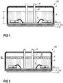
- the power semiconductor module arrangement 100 includes a housing 7 and a semiconductor substrate 10.
- the semiconductor substrate 10 includes a dielectric insulation layer 11, a (structured) first metallization layer 111 attached to the dielectric insulation layer 11, and a second (structured) metallization layer 112 attached to the dielectric insulation layer 11.
- the dielectric insulation layer 11 is disposed between the first and second metallization layers 111, 112.
- Each of the first and second metallization layers 111, 112 may consist of or include one of the following materials: copper; a copper alloy; aluminium; an aluminium alloy; any other metal or alloy that remains solid during the operation of the power semiconductor module arrangement.
- the semiconductor substrate 10 may be a ceramic substrate, that is, a substrate in which the dielectric insulation layer 11 is a ceramic, e.g., a thin ceramic layer.
- the ceramic may consist of or include one of the following materials: aluminium oxide; aluminium nitride; zirconium oxide; silicon nitride; boron nitride; or any other dielectric ceramic.
- the dielectric insulation layer 11 may consist of or include one of the following materials: Al 2 O 3 , AlN, SiC, BeO or Si 3 N 4 .
- the substrate 10 may, e.g., be a Direct Copper Bonding (DCB) substrate, a Direct Aluminium Bonding (DAB) substrate, or an Active Metal Brazing (AMB) substrate.
- the substrate 10 may also be a conventional printed circuit board (PCB) having a non-ceramic dielectric insulation layer 11.
- a non-ceramic dielectric insulation layer 11 may consist of or include a cured resin.
- the semiconductor substrate 10 is arranged in a housing 7.
- the semiconductor substrate 10 forms a ground surface of the housing 7, while the housing 7 itself solely comprises sidewalls and a cover. This is, however, only an example. It is also possible that the housing 7 further comprises a ground surface and the semiconductor substrate 10 is arranged inside the housing 7.
- the semiconductor substrate 10 may be mounted on a base plate (not illustrated). In some power semiconductor module arrangements 100, more than one semiconductor substrate 10 is arranged on a single base plate. The base plate may form a ground surface of the housing 7, for example.
- One or more semiconductor bodies 20 may be arranged on the semiconductor substrate 10.
- Each of the semiconductor bodies 20 arranged on the semiconductor substrate 10 may include a diode, an IGBT (Insulated-Gate Bipolar Transistor), a MOSFET (Metal-Oxide-Semiconductor Field-Effect Transistor), a JFET (Junction Field-Effect Transistor), a HEMT (High-Electron-Mobility Transistor), or any other suitable controllable semiconductor element.
- IGBT Insulated-Gate Bipolar Transistor
- MOSFET Metal-Oxide-Semiconductor Field-Effect Transistor
- JFET Joint Field-Effect Transistor
- HEMT High-Electron-Mobility Transistor
- the one or more semiconductor bodies 20 may form a semiconductor arrangement on the semiconductor substrate 10.
- the second metallization layer 112 of the semiconductor substrate 10 in Figure 1 is a continuous layer.
- the first metallization layer 111 is a structured layer in the example illustrated in Figure 1 .
- "Structured layer” means that the first metallization layer 111 is not a continuous layer, but includes recesses between different sections of the layer. Such recesses are schematically illustrated in Figure 1 .
- the first metallization layer 111 in this example includes three different sections. Different semiconductor bodies 20 may be mounted to the same or to different sections of the first metallization layer 111.
- Different sections of the first metallization layer may have no electrical connection or may be electrically connected to one or more other sections using, e.g., bonding wires 3.
- Electrical connections 3 may also include connection plates or conductor rails, for example, to name just a few examples.
- the one or more semiconductor bodies 20 may be electrically and mechanically connected to the semiconductor substrate 10 by an electrically conductive connection layer 30.
- Such an electrically conductive connection layer may be a solder layer, a layer of an electrically conductive adhesive, or a layer of a sintered metal powder, e.g., a sintered silver powder, for example.
- the power semiconductor module arrangement 100 further includes terminal elements 4.
- the terminal elements 4 are electrically connected to the first metallization layer 111 and provide an electrical connection between the inside and the outside of the housing 7.
- the terminal elements 4 may be electrically connected to the first metallization layer 111 with a first end, while a second end 41 of the terminal elements 4 protrudes out of the housing 7.
- the terminal elements 4 may be electrically contacted from the outside at their second end 41.
- the semiconductor bodies 20 each may include a chip pad metallization, e.g., a source, drain, anode, cathode or gate metallization.
- a chip pad metallization generally provides a contact surface for electrically connecting the semiconductor body 20.
- the chip pad metallization may electrically contact a connection layer 30, a terminal element 4, or an electrical connection 3, for example.
- a chip pad metallization may consist of or include a metal such as aluminium, copper, gold or silver, for example.
- the electrical connections 3 and the terminal elements 4 may also consist of or include a metal such as copper, aluminium, gold, or silver, for example.
- Corrosive gases may include, e.g., sulfur or sulfur-containing compounds. Corrosive gases in the surrounding area of the power semiconductor module arrangement 100 may penetrate into the inside of the housing 7.
- the housings 7 that are used for power semiconductor module arrangements 100 are usually not fully protected against protruding gases.
- corrosive gases may enter the housing 7 when the housing 7 is opened or before the housing 7 is closed, for example. Inside the housing 7, the corrosive gases may form acids or solutions, for example, in combination with moisture that is present inside the housing 7. The corrosive gases or the resulting solutions may cause a corrosion of some or all of the components.
- the metallic constituents of the components may be oxidized to their respective sulfides.
- the sulfide formation may alter the electrical properties of the components or may result in the formation of new conductive connections and in short circuits within the power semiconductor module arrangement 100.
- H 2 S hydrogen sulfide
- OCS carbonyl sulfide
- Ss gaseous sulfur
- Components including one or more metals such as copper (e.g., first metallization layer 111, electrical connection 3, terminal element 4, connection layer 30, chip pad metallization), silver (e.g., first metallization layer 111, electrical connection 3, terminal element 4, connection layer 30, chip pad metallization), or lead (e.g. connection layer 30 including leaded solder), may be particularly sensitive to corrosion.
- metals such as copper, for example, may have a thin oxide layer covering their surface area, which may provide at least a certain amount of protection against corrosive gases.
- the power semiconductor module arrangement 100 generally further includes a casting compound 5.
- the casting compound 5 may consist of or include a silicone gel or may be a rigid molding compound, for example.
- the casting compound 5 may at least partly fil the interior of the housing 7, thereby covering the components and electrical connections that are arranged on the semiconductor substrate 10.
- the terminal elements 4 may be partly embedded in the casting compound 5. At least their second ends 41, however, are not covered by the casting compound 5 and protrude from the casting compound 5 through the housing 7 to the outside of the housing 7.
- the casting compound 5 is configured to protect the components and electrical connections inside the power semiconductor module 100, in particular inside the housing 7, from certain environmental conditions and mechanical damage. However, corrosive gases are usually able to penetrate through the casting compound 5.
- the casting compound 5, therefore, is usually not able to protect the components and electrical connections from corrosive gases.
- the casting compound 5 may form a first protective layer with a first thickness d1 in a vertical direction.
- the vertical direction is a direction that is essentially perpendicular to a top surface of the semiconductor module 10.
- the top surface of the semiconductor module 10 is a surface to which semiconductor bodies 20 are or may be mounted.
- the first protective layer 5 at least partly covers any components that are arranged on the top surface of the semiconductor substrate 10 as well as any exposed surfaces of the semiconductor substrate 10.
- the first thickness d1 may be between 1mm and 10mm, for example.
- the power semiconductor module arrangement 100 further includes a second protective layer 6.
- the second protective layer 6 is arranged on a top surface of the first protective layer 5.
- the top surface of the first protective layer 5 is a surface opposite to its lower surface, wherein the lower surface covers the components and the semiconductor substrate 10.
- the second protective layer 6 is configured to seal at least a part of the inside of the housing 7.
- the inside of the housing 7 may be divided in two areas, namely a first area in which the semiconductor substrate 10 and any components and electrical connections mounted to the semiconductor substrate 10 are arranged, and a second area which does not include any major components.
- the first protective layer 5 may form an essential part of the first area.
- the terminal elements 4 may pass from the semiconductor substrate 10 through the first area (first protective layer 5) and through the second area to the outside of the housing 7. Without a second protective layer 6, corrosive gases may, for example, penetrate the second area and then reach the components of the semiconductor arrangement through the first area.
- the second protective layer 6 may be arranged between the first area and the second area, thereby protecting the first area and any components arranged in the first area against the corrosive gases.
- Corrosive gases for example, may enter the second area of the inside of the housing 7 through the openings that allow the terminal elements 4 to pass through the housing 7. The corrosive gases, however, are prevented from entering the first area by the second protective layer 6.
- the second protective layer 6 may have a second thickness d2 in the vertical direction.
- the second thickness d2 may be between 0.3mm and 10mm, for example.
- the second protective layer 6 may include a first material.
- the first material may be a dielectric material.
- the second protective layer 6 may further include a reactant 61.
- the reactant 61 is configured to chemically react with the corrosive gases, or, in particular, with the sulfur or sulfur-containing compounds of the corrosive gases. Corrosive gas may also be trapped, adsorbed or absorbed by the reactant 61. By chemically reacting with the corrosive gas, the reactant 61 prevents the harmful substances from reaching the (metal) components inside the housing 7 and thereby protects the components against corrosion.
- the reactant 61 may be, for example, a powder of a second material which is distributed throughout the first material of the second protective layer 6.
- the second material may include a metallic material such as, e.g., Ag, Fe, Co, Ni, Cu, Sn, Pb, Mn or may include activated carbon, for example. These are, however, only examples. Any additional or alternative materials which react with the corrosive gases and which may, e.g., form a metal sulfide when exposed to corrosive gases, are also possible.
- the reactant 61 may be essentially evenly distributed throughout the protective layer 6.
- the first material may consist of or include a non-reactive polymer such as a silicone gel or silicone rubber, for example. Other casting materials are also possible such as epoxy resin, for example.
- the concentration of the second material in the second protective layer 6 may be such that the second protective layer 6 as a whole is still electrically insulating.
- the second protective layer 6 may be provided as a separate layer or mat.
- the protective layer 6 may be produced separately and subsequently be inserted into the housing 7.
- the second protective layer 6 may include several parts, as is exemplarily illustrated in Figure 3 . In other arrangements, however, the second protective layer 6 may only include one part, as is exemplarily illustrated in Figure 4 . Generally, it depends on the geometry of the power semiconductor module arrangement 100 whether the second protective layer 6 includes only a single part or more than one part.
- the terminal elements 4 are arranged away from the sidewalls of the housing. For example, a distance between the terminal elements 4 and the sidewalls of the housing may be more than 0.1mm, more than 1mm or more than 10mm. In the example illustrated in Figure 4 , the terminal elements 4 are arranged close to the sidewalls of the housing 7, which means that a distance between each terminal element 4 and at least one sidewall is essentially zero.
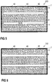
- Figure 5 exemplarily illustrates a top view of the arrangement of Figure 3 .
- the terminal elements 4 may be elongated in a first horizontal direction.
- the first horizontal direction is a direction that is essentially parallel to the top surface of the semiconductor substrate 10.
- the terminal elements 4 may be continuous elements extending from a first sidewall of the housing 7 to an opposite sidewall of the housing (e.g., top terminal element in Figure 5 ).
- the terminal elements 4, however, may also include one or more recesses (e.g., bottom terminal element 4 in Figure 5 ).
- the gap between the terminal element 4 and at least one of the sidewalls is optional.
- each terminal element 4 adjoins one of the sidewalls with a first end and adjoins a second sidewall, opposite to the first sidewall, with a second end.
- the power semiconductor module arrangement 100 may optionally further include auxiliary terminals 40.
- auxiliary terminals 40 may be arranged adjacent to one or more sidewalls of the housing 7. According to another example, there may be a gap between at least one of the auxiliary terminals 40 and the sidewalls of the housing 7.
- the auxiliary terminals 40 may also be configured to provide an electrical connection between the semiconductor substrate 10 and the outside of the housing 7.
- the terminal elements 4 as well as the auxiliary terminals 40 are each arranged adjacent to at least one sidewall of the housing 7.
- Figure 7 exemplarily illustrates a top view of the power semiconductor module arrangement of Figure 4 .
- the second protective layer 6 may be a continuous layer (see Figures 5 and 7 ) which includes openings and recesses through which the terminal elements 4 and auxiliary terminals 40 may pass.
- the dimensions of the second protective layer 6 depend on the size and the shape of the housing 7 and the size, shape and positions of the terminal elements 4 and/or the auxiliary terminals 40.
- the protective layer 6 may be produced as a flexible mat.
- the flexible mat may be produced separately and may be arranged on the top surface of the first protective layer 5. It is, however, generally also possible that the second protective layer 6 is produced as a rigid plate instead of a flexible mat.
- the hardness of plastics and rubbers is generally defined as a material's resistance to permanent indentation.
- the hardness of plastics and rubbers is often measured by the so-called durometer hardness method, also known as shore hardness method.
- durometer hardness method also known as shore hardness method.
- the second protective layer 6 may have a hardness in the range of Shore A x-y, for example. A layer with a hardness within the given range is not very sticking and, therefore, rather easy to handle.
- the second protective layer 6 may be produced by any suitable process such as casting or molding, for example.
- the materials forming the second protective layer 6, in particular the first material may originally be in a liquid or viscous form.
- a mixture may be produced by mixing the first material and the second material.
- the mixture may then be filled into a casting mold, for example. After filling the mixture into the casting mold, the mixture may be developed (processed) into a solid or semi-solid mat or plate with the second material evenly distributed therein.
- the casting mold may have a simple rectangular or quadratic form, for example.
- the resulting mat or plate therefore, may also have a rectangular or quadratic form.
- Recesses for the terminal elements 4 or auxiliary terminals 40 may be cut out in a further step to adapt the form of the mat or plate to the geometry of the power semiconductor module arrangement 100.
- an extrusion method may be used to shape the mat or plate. Extrusion methods are generally used to create objects of a fixed cross-sectional profile. A material (e.g., the solid or semi-solid mat or plate) is pushed through a die or press mold of the desired cross-section. In this way, very complex cross-sections of the mat or plate may be created. It is, however, also possible that the casting mold includes respective recesses such that the mat or plate is casted or molded in the desired shape without the need for a further cutting step.
- the mat or plate may subsequently be removed from the casting mold.
- the mat or plate may be produced by a supplier.
- the manufacturer of the power semiconductor module arrangement 100 may buy the finished mat or plate and may insert the mat or plate into a power semiconductor module arrangement during the mounting process. The manufacturer, however, does not need to perform a molding step and/or a curing or hardening process when assembling the power semiconductor module arrangement 100.
- the mat or plate does not have a substance-to-substance bond with any of the other components of the power semiconductor module arrangement 100. In other words, it would be generally possible to remove the mat or plate from the power semiconductor module arrangement 100, without destroying any of the other components.
- the mat or plate does not have a substance-to-substance bond with the sidewalls of the housing.
- the mat or plate may have a certain adhesive strength and may adhere to the sidewalls to a certain degree. However, this is not a permanent bond. The same applies to the bond between the mat or plate and the first protection layer 5.
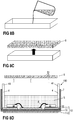
- Figure 8 The method described above is schematically illustrated in Figure 8 , wherein Figure 8A illustrates the step of mixing the first material and the second material.
- Figure 8B illustrates the step of filling the mixture into the casting mold.
- the mat or plate 6 is removed from the casting mold.
- the prefabricated mat or plate 6 may be inserted in the housing 7 of a power semiconductor module arrangement 100, as has been described above.
Landscapes
- Structures Or Materials For Encapsulating Or Coating Semiconductor Devices Or Solid State Devices (AREA)
Priority Applications (1)
| Application Number | Priority Date | Filing Date | Title |
|---|---|---|---|
| EP17178592.6A EP3422399B1 (de) | 2017-06-29 | 2017-06-29 | Verfahren zur herstellung einer vorrichtung zum schutz eines halbleitermoduls und halbleitermodul mit dieser vorrichtung |
Applications Claiming Priority (1)
| Application Number | Priority Date | Filing Date | Title |
|---|---|---|---|
| EP17178592.6A EP3422399B1 (de) | 2017-06-29 | 2017-06-29 | Verfahren zur herstellung einer vorrichtung zum schutz eines halbleitermoduls und halbleitermodul mit dieser vorrichtung |
Publications (2)
| Publication Number | Publication Date |
|---|---|
| EP3422399A1 true EP3422399A1 (de) | 2019-01-02 |
| EP3422399B1 EP3422399B1 (de) | 2024-07-31 |
Family
ID=59285020
Family Applications (1)
| Application Number | Title | Priority Date | Filing Date |
|---|---|---|---|
| EP17178592.6A Active EP3422399B1 (de) | 2017-06-29 | 2017-06-29 | Verfahren zur herstellung einer vorrichtung zum schutz eines halbleitermoduls und halbleitermodul mit dieser vorrichtung |
Country Status (1)
| Country | Link |
|---|---|
| EP (1) | EP3422399B1 (de) |
Cited By (8)
| Publication number | Priority date | Publication date | Assignee | Title |
|---|---|---|---|---|
| EP3667717A1 (de) * | 2018-12-11 | 2020-06-17 | ABB Schweiz AG | Leistungselektronikmodul |
| EP3770962A1 (de) * | 2019-07-26 | 2021-01-27 | Infineon Technologies AG | Halbleitermodulanordnung |
| CN113451219A (zh) * | 2020-03-24 | 2021-09-28 | 英飞凌科技股份有限公司 | 在与安装基座的模块接口处具有气流抑制密封部的模块 |
| CN114190020A (zh) * | 2020-09-14 | 2022-03-15 | 罗克韦尔自动化技术公司 | 对气态腐蚀性空气具有增强保护的电力转换系统 |
| EP4064328A1 (de) * | 2021-03-25 | 2022-09-28 | Infineon Technologies AG | Gehäuse, halbleitermodul und verfahren zur herstellung davon |
| US11605917B2 (en) | 2020-09-14 | 2023-03-14 | Rockwell Automation Technologies, Inc. | Protective cover devices for protecting electrical connectors in industrial equipment |
| US20230326820A1 (en) * | 2022-04-07 | 2023-10-12 | Infineon Technologies Ag | Anti-Corrosion Particles in Semiconductor Device |
| WO2025096035A1 (en) * | 2023-11-03 | 2025-05-08 | Wolfspeed, Inc. | Power modules having encapsulation stress and strain mitigating configurations |
Citations (5)
| Publication number | Priority date | Publication date | Assignee | Title |
|---|---|---|---|---|
| JP3456257B2 (ja) * | 1994-05-27 | 2003-10-14 | 株式会社デンソー | 電子素子用パッケージ |
| US20090084602A1 (en) * | 2007-09-28 | 2009-04-02 | Shin-Etsu Chemical Co., Ltd. | Automotive electric/electronic package |
| US20130011998A1 (en) * | 2010-03-31 | 2013-01-10 | Lintec Corporation | Resin Film Forming Sheet for Chip, and Method for Manufacturing Semiconductor Chip |
| US20150001700A1 (en) * | 2013-06-28 | 2015-01-01 | Infineon Technologies Ag | Power Modules with Parylene Coating |
| US20170162461A1 (en) * | 2015-12-08 | 2017-06-08 | Infineon Technologies Austria Ag | Semiconductor Device and Method of Manufacturing Thereof |
-
2017
- 2017-06-29 EP EP17178592.6A patent/EP3422399B1/de active Active
Patent Citations (5)
| Publication number | Priority date | Publication date | Assignee | Title |
|---|---|---|---|---|
| JP3456257B2 (ja) * | 1994-05-27 | 2003-10-14 | 株式会社デンソー | 電子素子用パッケージ |
| US20090084602A1 (en) * | 2007-09-28 | 2009-04-02 | Shin-Etsu Chemical Co., Ltd. | Automotive electric/electronic package |
| US20130011998A1 (en) * | 2010-03-31 | 2013-01-10 | Lintec Corporation | Resin Film Forming Sheet for Chip, and Method for Manufacturing Semiconductor Chip |
| US20150001700A1 (en) * | 2013-06-28 | 2015-01-01 | Infineon Technologies Ag | Power Modules with Parylene Coating |
| US20170162461A1 (en) * | 2015-12-08 | 2017-06-08 | Infineon Technologies Austria Ag | Semiconductor Device and Method of Manufacturing Thereof |
Cited By (21)
| Publication number | Priority date | Publication date | Assignee | Title |
|---|---|---|---|---|
| EP3667717A1 (de) * | 2018-12-11 | 2020-06-17 | ABB Schweiz AG | Leistungselektronikmodul |
| EP3770962A1 (de) * | 2019-07-26 | 2021-01-27 | Infineon Technologies AG | Halbleitermodulanordnung |
| US11538725B2 (en) | 2019-07-26 | 2022-12-27 | Infineon Technologies Ag | Semiconductor module arrangement |
| US11615994B2 (en) | 2020-03-24 | 2023-03-28 | Infineon Technologies Ag | Module with gas flow-inhibiting sealing at module interface to mounting base |
| CN113451219A (zh) * | 2020-03-24 | 2021-09-28 | 英飞凌科技股份有限公司 | 在与安装基座的模块接口处具有气流抑制密封部的模块 |
| EP3886155A1 (de) * | 2020-03-24 | 2021-09-29 | Infineon Technologies AG | Modul mit gasflusshemmender abdichtung an der modulschnittstelle zum montagesockel |
| US12519023B2 (en) | 2020-03-24 | 2026-01-06 | Infineon Technologies Ag | Module with gas flow-inhibiting sealing at module interface to mounting base |
| CN113451219B (zh) * | 2020-03-24 | 2025-06-17 | 英飞凌科技股份有限公司 | 在与安装基座的模块接口处具有气流抑制密封部的模块 |
| EP4231795A2 (de) | 2020-09-14 | 2023-08-23 | Rockwell Automation Technologies, Inc. | Stromumwandlungssystem mit verbessertem schutz für gasförmige korrosive atmosphären |
| US11605917B2 (en) | 2020-09-14 | 2023-03-14 | Rockwell Automation Technologies, Inc. | Protective cover devices for protecting electrical connectors in industrial equipment |
| US11784554B2 (en) | 2020-09-14 | 2023-10-10 | Rockwell Automation Technologies, Inc. | Power conversion system with enhanced protection for gaseous corrosive atmospheres |
| EP4231795A3 (de) * | 2020-09-14 | 2023-11-08 | Rockwell Automation Technologies, Inc. | Stromumwandlungssystem mit verbessertem schutz für gasförmige korrosive atmosphären |
| CN114190020B (zh) * | 2020-09-14 | 2024-02-13 | 罗克韦尔自动化技术公司 | 对气态腐蚀性空气具有增强保护的电力转换系统 |
| US11901667B2 (en) | 2020-09-14 | 2024-02-13 | Rockwell Automation Technologies, Inc. | Protective cover devices for protecting electrical connectors in industrial equipment |
| US12009740B2 (en) | 2020-09-14 | 2024-06-11 | Rockwell Automation Technologies, Inc. | Power conversion system with enhanced protection for gaseous corrosive atmospheres |
| EP3968741A1 (de) | 2020-09-14 | 2022-03-16 | Rockwell Automation Technologies, Inc. | Stromumwandlungssystem mit verbessertem schutz für gasförmige korrosive atmosphären |
| CN114190020A (zh) * | 2020-09-14 | 2022-03-15 | 罗克韦尔自动化技术公司 | 对气态腐蚀性空气具有增强保护的电力转换系统 |
| EP4064328A1 (de) * | 2021-03-25 | 2022-09-28 | Infineon Technologies AG | Gehäuse, halbleitermodul und verfahren zur herstellung davon |
| US12148718B2 (en) | 2021-03-25 | 2024-11-19 | Infineon Technologies Ag | Housing, semiconductor module and methods for producing the same |
| US20230326820A1 (en) * | 2022-04-07 | 2023-10-12 | Infineon Technologies Ag | Anti-Corrosion Particles in Semiconductor Device |
| WO2025096035A1 (en) * | 2023-11-03 | 2025-05-08 | Wolfspeed, Inc. | Power modules having encapsulation stress and strain mitigating configurations |
Also Published As
| Publication number | Publication date |
|---|---|
| EP3422399B1 (de) | 2024-07-31 |
Similar Documents
| Publication | Publication Date | Title |
|---|---|---|
| EP3422399B1 (de) | Verfahren zur herstellung einer vorrichtung zum schutz eines halbleitermoduls und halbleitermodul mit dieser vorrichtung | |
| US11848213B2 (en) | Semiconductor module having a layer that includes inorganic filler and a casting material | |
| US11978700B2 (en) | Power semiconductor module arrangement | |
| US20240429181A1 (en) | Method for forming a lid of a housing | |
| US8097934B1 (en) | Delamination resistant device package having low moisture sensitivity | |
| JP6797951B2 (ja) | パワー半導体モジュール装置及びその製造方法 | |
| US20080191340A1 (en) | Power Semiconductor Module And Method For Its Manufacture | |
| US11699625B2 (en) | Power semiconductor module arrangement | |
| EP3913665B1 (de) | Leistungshalbleitermodul und verfahren zur herstellung eines leistungshalbleitermoduls | |
| JP2000340718A (ja) | 電力用半導体装置 | |
| EP3731267A1 (de) | Halbleitermodul und verfahren zur herstellung davon | |
| EP3806142B1 (de) | Halbleitermodul und verfahren zu seiner herstellung | |
| EP4489067B1 (de) | Gehäuse, halbleitermodul und verfahren zu dessen herstellung | |
| US20260090385A1 (en) | Semiconductor module comprising a housing | |
| JP7661982B2 (ja) | 半導体装置 | |
| CN111128752B (zh) | 接触元件,具有接触元件的功率半导体模块和用于制造接触元件的方法 | |
| CN120511235A (zh) | 半导体模块装置、用于半导体模块装置的电子器件载体以及用于制造半导体模块装置的方法 |
Legal Events
| Date | Code | Title | Description |
|---|---|---|---|
| PUAI | Public reference made under article 153(3) epc to a published international application that has entered the european phase |
Free format text: ORIGINAL CODE: 0009012 |
|
| STAA | Information on the status of an ep patent application or granted ep patent |
Free format text: STATUS: THE APPLICATION HAS BEEN PUBLISHED |
|
| AK | Designated contracting states |
Kind code of ref document: A1 Designated state(s): AL AT BE BG CH CY CZ DE DK EE ES FI FR GB GR HR HU IE IS IT LI LT LU LV MC MK MT NL NO PL PT RO RS SE SI SK SM TR |
|
| AX | Request for extension of the european patent |
Extension state: BA ME |
|
| STAA | Information on the status of an ep patent application or granted ep patent |
Free format text: STATUS: REQUEST FOR EXAMINATION WAS MADE |
|
| 17P | Request for examination filed |
Effective date: 20190103 |
|
| RBV | Designated contracting states (corrected) |
Designated state(s): AL AT BE BG CH CY CZ DE DK EE ES FI FR GB GR HR HU IE IS IT LI LT LU LV MC MK MT NL NO PL PT RO RS SE SI SK SM TR |
|
| STAA | Information on the status of an ep patent application or granted ep patent |
Free format text: STATUS: EXAMINATION IS IN PROGRESS |
|
| 17Q | First examination report despatched |
Effective date: 20201029 |
|
| GRAP | Despatch of communication of intention to grant a patent |
Free format text: ORIGINAL CODE: EPIDOSNIGR1 |
|
| STAA | Information on the status of an ep patent application or granted ep patent |
Free format text: STATUS: GRANT OF PATENT IS INTENDED |
|
| INTG | Intention to grant announced |
Effective date: 20240403 |
|
| GRAS | Grant fee paid |
Free format text: ORIGINAL CODE: EPIDOSNIGR3 |
|
| P01 | Opt-out of the competence of the unified patent court (upc) registered |
Effective date: 20240507 |
|
| GRAA | (expected) grant |
Free format text: ORIGINAL CODE: 0009210 |
|
| STAA | Information on the status of an ep patent application or granted ep patent |
Free format text: STATUS: THE PATENT HAS BEEN GRANTED |
|
| AK | Designated contracting states |
Kind code of ref document: B1 Designated state(s): AL AT BE BG CH CY CZ DE DK EE ES FI FR GB GR HR HU IE IS IT LI LT LU LV MC MK MT NL NO PL PT RO RS SE SI SK SM TR |
|
| REG | Reference to a national code |
Ref country code: CH Ref legal event code: EP Ref country code: GB Ref legal event code: FG4D |
|
| REG | Reference to a national code |
Ref country code: DE Ref legal event code: R096 Ref document number: 602017083654 Country of ref document: DE |
|
| REG | Reference to a national code |
Ref country code: IE Ref legal event code: FG4D |
|
| REG | Reference to a national code |
Ref country code: LT Ref legal event code: MG9D |
|
| REG | Reference to a national code |
Ref country code: NL Ref legal event code: MP Effective date: 20240731 |
|
| PG25 | Lapsed in a contracting state [announced via postgrant information from national office to epo] |
Ref country code: PT Free format text: LAPSE BECAUSE OF FAILURE TO SUBMIT A TRANSLATION OF THE DESCRIPTION OR TO PAY THE FEE WITHIN THE PRESCRIBED TIME-LIMIT Effective date: 20241202 |
|
| REG | Reference to a national code |
Ref country code: AT Ref legal event code: MK05 Ref document number: 1709313 Country of ref document: AT Kind code of ref document: T Effective date: 20240731 |
|
| PG25 | Lapsed in a contracting state [announced via postgrant information from national office to epo] |
Ref country code: PT Free format text: LAPSE BECAUSE OF FAILURE TO SUBMIT A TRANSLATION OF THE DESCRIPTION OR TO PAY THE FEE WITHIN THE PRESCRIBED TIME-LIMIT Effective date: 20241202 |
|
| PG25 | Lapsed in a contracting state [announced via postgrant information from national office to epo] |
Ref country code: NO Free format text: LAPSE BECAUSE OF FAILURE TO SUBMIT A TRANSLATION OF THE DESCRIPTION OR TO PAY THE FEE WITHIN THE PRESCRIBED TIME-LIMIT Effective date: 20241031 |
|
| PG25 | Lapsed in a contracting state [announced via postgrant information from national office to epo] |
Ref country code: NL Free format text: LAPSE BECAUSE OF FAILURE TO SUBMIT A TRANSLATION OF THE DESCRIPTION OR TO PAY THE FEE WITHIN THE PRESCRIBED TIME-LIMIT Effective date: 20240731 Ref country code: PL Free format text: LAPSE BECAUSE OF FAILURE TO SUBMIT A TRANSLATION OF THE DESCRIPTION OR TO PAY THE FEE WITHIN THE PRESCRIBED TIME-LIMIT Effective date: 20240731 Ref country code: FI Free format text: LAPSE BECAUSE OF FAILURE TO SUBMIT A TRANSLATION OF THE DESCRIPTION OR TO PAY THE FEE WITHIN THE PRESCRIBED TIME-LIMIT Effective date: 20240731 Ref country code: GR Free format text: LAPSE BECAUSE OF FAILURE TO SUBMIT A TRANSLATION OF THE DESCRIPTION OR TO PAY THE FEE WITHIN THE PRESCRIBED TIME-LIMIT Effective date: 20241101 |
|
| PG25 | Lapsed in a contracting state [announced via postgrant information from national office to epo] |
Ref country code: BG Free format text: LAPSE BECAUSE OF FAILURE TO SUBMIT A TRANSLATION OF THE DESCRIPTION OR TO PAY THE FEE WITHIN THE PRESCRIBED TIME-LIMIT Effective date: 20240731 |
|
| PG25 | Lapsed in a contracting state [announced via postgrant information from national office to epo] |
Ref country code: LV Free format text: LAPSE BECAUSE OF FAILURE TO SUBMIT A TRANSLATION OF THE DESCRIPTION OR TO PAY THE FEE WITHIN THE PRESCRIBED TIME-LIMIT Effective date: 20240731 |
|
| PG25 | Lapsed in a contracting state [announced via postgrant information from national office to epo] |
Ref country code: IS Free format text: LAPSE BECAUSE OF FAILURE TO SUBMIT A TRANSLATION OF THE DESCRIPTION OR TO PAY THE FEE WITHIN THE PRESCRIBED TIME-LIMIT Effective date: 20241130 Ref country code: AT Free format text: LAPSE BECAUSE OF FAILURE TO SUBMIT A TRANSLATION OF THE DESCRIPTION OR TO PAY THE FEE WITHIN THE PRESCRIBED TIME-LIMIT Effective date: 20240731 |
|
| PG25 | Lapsed in a contracting state [announced via postgrant information from national office to epo] |
Ref country code: HR Free format text: LAPSE BECAUSE OF FAILURE TO SUBMIT A TRANSLATION OF THE DESCRIPTION OR TO PAY THE FEE WITHIN THE PRESCRIBED TIME-LIMIT Effective date: 20240731 |
|
| PG25 | Lapsed in a contracting state [announced via postgrant information from national office to epo] |
Ref country code: ES Free format text: LAPSE BECAUSE OF FAILURE TO SUBMIT A TRANSLATION OF THE DESCRIPTION OR TO PAY THE FEE WITHIN THE PRESCRIBED TIME-LIMIT Effective date: 20240731 Ref country code: RS Free format text: LAPSE BECAUSE OF FAILURE TO SUBMIT A TRANSLATION OF THE DESCRIPTION OR TO PAY THE FEE WITHIN THE PRESCRIBED TIME-LIMIT Effective date: 20241031 |
|
| PG25 | Lapsed in a contracting state [announced via postgrant information from national office to epo] |
Ref country code: RS Free format text: LAPSE BECAUSE OF FAILURE TO SUBMIT A TRANSLATION OF THE DESCRIPTION OR TO PAY THE FEE WITHIN THE PRESCRIBED TIME-LIMIT Effective date: 20241031 Ref country code: PL Free format text: LAPSE BECAUSE OF FAILURE TO SUBMIT A TRANSLATION OF THE DESCRIPTION OR TO PAY THE FEE WITHIN THE PRESCRIBED TIME-LIMIT Effective date: 20240731 Ref country code: NO Free format text: LAPSE BECAUSE OF FAILURE TO SUBMIT A TRANSLATION OF THE DESCRIPTION OR TO PAY THE FEE WITHIN THE PRESCRIBED TIME-LIMIT Effective date: 20241031 Ref country code: NL Free format text: LAPSE BECAUSE OF FAILURE TO SUBMIT A TRANSLATION OF THE DESCRIPTION OR TO PAY THE FEE WITHIN THE PRESCRIBED TIME-LIMIT Effective date: 20240731 Ref country code: LV Free format text: LAPSE BECAUSE OF FAILURE TO SUBMIT A TRANSLATION OF THE DESCRIPTION OR TO PAY THE FEE WITHIN THE PRESCRIBED TIME-LIMIT Effective date: 20240731 Ref country code: IS Free format text: LAPSE BECAUSE OF FAILURE TO SUBMIT A TRANSLATION OF THE DESCRIPTION OR TO PAY THE FEE WITHIN THE PRESCRIBED TIME-LIMIT Effective date: 20241130 Ref country code: HR Free format text: LAPSE BECAUSE OF FAILURE TO SUBMIT A TRANSLATION OF THE DESCRIPTION OR TO PAY THE FEE WITHIN THE PRESCRIBED TIME-LIMIT Effective date: 20240731 Ref country code: GR Free format text: LAPSE BECAUSE OF FAILURE TO SUBMIT A TRANSLATION OF THE DESCRIPTION OR TO PAY THE FEE WITHIN THE PRESCRIBED TIME-LIMIT Effective date: 20241101 Ref country code: FI Free format text: LAPSE BECAUSE OF FAILURE TO SUBMIT A TRANSLATION OF THE DESCRIPTION OR TO PAY THE FEE WITHIN THE PRESCRIBED TIME-LIMIT Effective date: 20240731 Ref country code: ES Free format text: LAPSE BECAUSE OF FAILURE TO SUBMIT A TRANSLATION OF THE DESCRIPTION OR TO PAY THE FEE WITHIN THE PRESCRIBED TIME-LIMIT Effective date: 20240731 Ref country code: BG Free format text: LAPSE BECAUSE OF FAILURE TO SUBMIT A TRANSLATION OF THE DESCRIPTION OR TO PAY THE FEE WITHIN THE PRESCRIBED TIME-LIMIT Effective date: 20240731 Ref country code: AT Free format text: LAPSE BECAUSE OF FAILURE TO SUBMIT A TRANSLATION OF THE DESCRIPTION OR TO PAY THE FEE WITHIN THE PRESCRIBED TIME-LIMIT Effective date: 20240731 |
|
| PG25 | Lapsed in a contracting state [announced via postgrant information from national office to epo] |
Ref country code: RO Free format text: LAPSE BECAUSE OF FAILURE TO SUBMIT A TRANSLATION OF THE DESCRIPTION OR TO PAY THE FEE WITHIN THE PRESCRIBED TIME-LIMIT Effective date: 20240731 Ref country code: SM Free format text: LAPSE BECAUSE OF FAILURE TO SUBMIT A TRANSLATION OF THE DESCRIPTION OR TO PAY THE FEE WITHIN THE PRESCRIBED TIME-LIMIT Effective date: 20240731 Ref country code: DK Free format text: LAPSE BECAUSE OF FAILURE TO SUBMIT A TRANSLATION OF THE DESCRIPTION OR TO PAY THE FEE WITHIN THE PRESCRIBED TIME-LIMIT Effective date: 20240731 |
|
| PG25 | Lapsed in a contracting state [announced via postgrant information from national office to epo] |
Ref country code: EE Free format text: LAPSE BECAUSE OF FAILURE TO SUBMIT A TRANSLATION OF THE DESCRIPTION OR TO PAY THE FEE WITHIN THE PRESCRIBED TIME-LIMIT Effective date: 20240731 |
|
| PG25 | Lapsed in a contracting state [announced via postgrant information from national office to epo] |
Ref country code: CZ Free format text: LAPSE BECAUSE OF FAILURE TO SUBMIT A TRANSLATION OF THE DESCRIPTION OR TO PAY THE FEE WITHIN THE PRESCRIBED TIME-LIMIT Effective date: 20240731 |
|
| PG25 | Lapsed in a contracting state [announced via postgrant information from national office to epo] |
Ref country code: IT Free format text: LAPSE BECAUSE OF FAILURE TO SUBMIT A TRANSLATION OF THE DESCRIPTION OR TO PAY THE FEE WITHIN THE PRESCRIBED TIME-LIMIT Effective date: 20240731 Ref country code: SK Free format text: LAPSE BECAUSE OF FAILURE TO SUBMIT A TRANSLATION OF THE DESCRIPTION OR TO PAY THE FEE WITHIN THE PRESCRIBED TIME-LIMIT Effective date: 20240731 |
|
| REG | Reference to a national code |
Ref country code: DE Ref legal event code: R097 Ref document number: 602017083654 Country of ref document: DE |
|
| PLBE | No opposition filed within time limit |
Free format text: ORIGINAL CODE: 0009261 |
|
| STAA | Information on the status of an ep patent application or granted ep patent |
Free format text: STATUS: NO OPPOSITION FILED WITHIN TIME LIMIT |
|
| 26N | No opposition filed |
Effective date: 20250501 |
|
| PG25 | Lapsed in a contracting state [announced via postgrant information from national office to epo] |
Ref country code: SE Free format text: LAPSE BECAUSE OF FAILURE TO SUBMIT A TRANSLATION OF THE DESCRIPTION OR TO PAY THE FEE WITHIN THE PRESCRIBED TIME-LIMIT Effective date: 20240731 |
|
| PGFP | Annual fee paid to national office [announced via postgrant information from national office to epo] |
Ref country code: DE Payment date: 20250822 Year of fee payment: 9 |
|
| REG | Reference to a national code |
Ref country code: DE Ref legal event code: R079 Ref document number: 602017083654 Country of ref document: DE Free format text: PREVIOUS MAIN CLASS: H01L0023240000 Ipc: H10W0076470000 |
|
| REG | Reference to a national code |
Ref country code: CH Ref legal event code: H13 Free format text: ST27 STATUS EVENT CODE: U-0-0-H10-H13 (AS PROVIDED BY THE NATIONAL OFFICE) Effective date: 20260127 |
|
| PG25 | Lapsed in a contracting state [announced via postgrant information from national office to epo] |
Ref country code: MC Free format text: LAPSE BECAUSE OF FAILURE TO SUBMIT A TRANSLATION OF THE DESCRIPTION OR TO PAY THE FEE WITHIN THE PRESCRIBED TIME-LIMIT Effective date: 20240731 |
|
| PG25 | Lapsed in a contracting state [announced via postgrant information from national office to epo] |
Ref country code: LU Free format text: LAPSE BECAUSE OF NON-PAYMENT OF DUE FEES Effective date: 20250629 |
|
| GBPC | Gb: european patent ceased through non-payment of renewal fee |
Effective date: 20250629 |
|
| REG | Reference to a national code |
Ref country code: BE Ref legal event code: MM Effective date: 20250630 |
|
| PG25 | Lapsed in a contracting state [announced via postgrant information from national office to epo] |
Ref country code: GB Free format text: LAPSE BECAUSE OF NON-PAYMENT OF DUE FEES Effective date: 20250629 |
|
| PG25 | Lapsed in a contracting state [announced via postgrant information from national office to epo] |
Ref country code: IE Free format text: LAPSE BECAUSE OF NON-PAYMENT OF DUE FEES Effective date: 20250629 |
|
| PG25 | Lapsed in a contracting state [announced via postgrant information from national office to epo] |
Ref country code: BE Free format text: LAPSE BECAUSE OF NON-PAYMENT OF DUE FEES Effective date: 20250630 |
|
| PG25 | Lapsed in a contracting state [announced via postgrant information from national office to epo] |
Ref country code: FR Free format text: LAPSE BECAUSE OF NON-PAYMENT OF DUE FEES Effective date: 20250630 |
|
| PG25 | Lapsed in a contracting state [announced via postgrant information from national office to epo] |
Ref country code: CH Free format text: LAPSE BECAUSE OF NON-PAYMENT OF DUE FEES Effective date: 20250630 |