EP3441793A1 - Réseau de scintillateurs - Google Patents
Réseau de scintillateurs Download PDFInfo
- Publication number
- EP3441793A1 EP3441793A1 EP17779141.5A EP17779141A EP3441793A1 EP 3441793 A1 EP3441793 A1 EP 3441793A1 EP 17779141 A EP17779141 A EP 17779141A EP 3441793 A1 EP3441793 A1 EP 3441793A1
- Authority
- EP
- European Patent Office
- Prior art keywords
- scintillator
- reaction
- neutron
- array according
- layer
- Prior art date
- Legal status (The legal status is an assumption and is not a legal conclusion. Google has not performed a legal analysis and makes no representation as to the accuracy of the status listed.)
- Granted
Links
Images




Classifications
-
- G—PHYSICS
- G01—MEASURING; TESTING
- G01T—MEASUREMENT OF NUCLEAR OR X-RADIATION
- G01T3/00—Measuring neutron radiation
- G01T3/06—Measuring neutron radiation with scintillation detectors
-
- G—PHYSICS
- G21—NUCLEAR PHYSICS; NUCLEAR ENGINEERING
- G21K—HANDLING OF PARTICLES OR IONISING RADIATION NOT OTHERWISE PROVIDED FOR; IRRADIATION DEVICES; GAMMA RAY OR X-RAY MICROSCOPES
- G21K4/00—Conversion screens for the conversion of the spatial distribution of X-rays or particle radiation into visible images, e.g. fluoroscopic screens
Definitions
- Embodiments of the present invention relate to a scintillator array.
- He-3 gas detector using 3 He (also referred to as He-3) gas which is an isotope of He (helium) and having high detection efficiency and a scintillation detector using a scintillator which reacts with neutrons directly or secondarily to emit light.
- a converter which reacts with neutrons to convert them into charged particles, gamma rays, or the like is required in order to detect the neutrons.
- the neutron converter there is known a neutron converter using 3 He, 6 Li (also referred to as Li-6), 10 B (also referred to as B-10), 113 Cd (Cd-113), 155 Gd (also referred to as Gd-155), 157 Gd (also referred to as Gd-157) or the like having a large neutron absorption cross section, but at present, a He-3 gas detector which is a neutron detector using He-3 gas is used because of low sensitivity to gamma rays.
- a neutron moderator such as polyethylene.
- the scintillation detector has a high counting capacity, density is high and sensitivity to gamma rays is high because of being a solid body.
- density is high and sensitivity to gamma rays is high because of being a solid body.
- it is essential to use a neutron detection scintillator having a short fluorescence lifetime. Therefore, a neutron detector using a scintillator constituted with a Li 2 B 4 O 7 single crystal for neutron detection and having a combination of its fluorescent property and a photomultiplier tube is under development.
- a scintillator constituted with a light element is preferable. Since Li, B, and O are each the light element, the scintillator constituted with the Li 2 B 4 O 7 single crystal satisfies the aforementioned demand.
- a neutron scintillator which is thinner compared with a conventional neutron scintillator and is more excellent in terms of gamma-ray sensitivity and position resolution compared with a conventional Li-based scintillator is under development.
- This can be produced by, using glass formed by adding Ce to an oxide containing B and Li as main components as a starting raw material, mixing Li 2 B 4 O7 and CeO 2 , thereafter heating the mixture at a temperature of at least 950°C or more and holding it for one hour or longer, and thereafter cooling it at a rate of 150°C/sec or more between temperatures of 800 and 400°C.
- LiBO 3 and Li 2 B 4 O 7 compounds constituted with only light elements estimated to have low gamma-ray sensitivity light emission by neutrons is very small.
- an amount of Ce solid-dissolving in the crystals is very small, the light emission by neutrons is small, and it is difficult to use them as a two-dimensional detector for neutron imaging or for neutron radiography.
- scintillator materials can be selected regardless of the gamma-ray sensitivity because a several MeV charged particle production reaction is used for the neutron detection.
- B can be expected to have neutron detection efficiency about four times of that of the same amount of Li, it is possible to produce a thinner scintillator.
- This scintillator since being very advantageous in terms of the gamma-ray sensitivity and the position resolution, is an ideal neutron converter.
- B has about half charged particle energy to be produced of that of commercially available Li glass (Li-Glass) and is considered disadvantageous in terms of light emission output, and in most of the conventional neutron scintillators, Li is used as a converter.
- neutron scintillator As a representative neutron scintillator which is practically used currently, for example, a neutron scintillator using LiF/ZnS can be cited.
- This neutron scintillator has a high light emission amount and is also excellent in handleability, but is opaque and is limited in detection efficiency and counting capacity.
- a resolution when high-definition imaging is performed depends on a spread in emitting light by putting a reactant and a scintillator together or on a resolution of an optical system or an image sensor which images the light.
- CCD charge coupled device
- CMOS complementary metal oxide semiconductor
- a flying distance (range) of the charged particles and a diffusion length of light emitted in the scintillator are one of causes to determine presence/absence of blurring related to the resolution.
- LiF/ZnS Li reacts with neutrons to emit alpha ( ⁇ ) rays, and the ⁇ rays make a ZnS phosphor emit light.
- An actual configuration, in which LiF/ZnS is granular powder, is a configuration in which the LiF/ZnS powder is applied on an Al plate being a substrate and bound by an organic binder, in many cases.
- Li-6 As Li which reacts with neutrons, Li-6 is normally used in order to increase reaction efficiency, but due to lowness of an atom density in relation to the whole including the binder or the like, an applied thickness is about several hundreds ⁇ m. Therefore, the resolution, which is determined by the applied thickness, is not high. When energy of neutrons in particular increases, a rate of reaction with Li-6 decreases further, and efficiency also becomes poor. Making the thickness larger is considered in order to increase the rate of reaction, but since LiF/ZnS is opaque and emitted light scatters in LiF/ZnS and is not transmitted, the efficiency does not increase even though the thickness is made larger.
- a two-dimensional detector in which a neutron detector is constituted with a capillary plate having a plurality of openings passing through in a thickness direction and filled with a liquid scintillator which reacts with neutrons in the plurality of these openings and an imaging detector, and which measures scintillation light.
- a neutron detector is constituted with a capillary plate having a plurality of openings passing through in a thickness direction and filled with a liquid scintillator which reacts with neutrons in the plurality of these openings and an imaging detector, and which measures scintillation light.
- the capillary plate portion does not react and the neutrons pass through this portion, a high-definition and high-efficiency two-dimensional detector is not obtained. It is also difficult, also from a manufacturing viewpoint, to hold the scintillator uniformly in all holes of the capillary plate, so that it is not practically used yet.
- an imaging intensifier which is obtained by combining a reaction film and a scintillator, converts light of the scintillator into electrons by using a photoelectric conversion film, and amplifies the electrons is also under development in order to achieve high definition and increase sensitivity.
- a thickness of the reaction film is only about 5 ⁇ m for the purpose of high definition, and reaction efficiency with neutrons is about 10% in a case of B-10, and remaining 90% of the neutrons is transmitted and is not used.
- the reaction efficiency decreases further. Therefore, the reaction efficiency is poor though definition is high, and when the number of generated neutrons is small (flux is small), it is necessary to perform integration over time.
- a problem to be solved by embodiments is to provide a scintillator array to be used for a neutron detector capable of detecting high energy neutrons with high definition and high efficiency.
- a scintillator array of the embodiment comprises a stack.
- the stack includes: a reaction part extending along one direction and configured to emit radiation by a reaction with neutrons; a scintillator part extending along the one direction, sandwiching the reaction part, and configured to emit light in response to the radiation; and a reflection part extending along the one direction and configured to reflect the light.
- the stack is configured to reflect the light on the reflection part and thus propagate the reflected light from an inside of the scintillator part to an outside of the scintillator part.
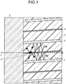
- FIG. 1 is a view illustrating a structure example of a scintillator array to be used for a neutron detector according to the embodiment.
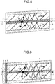
- FIG. 8 and FIG. 9 are views illustrating structure examples of scintillator arrays to be used for conventional neutron detectors.
- the scintillator array illustrated in FIG. 8 has granular scintillators 8 (for example, LiF/ZnS phosphors).
- granular scintillators 8 for example, LiF/ZnS phosphors.
- a transparent binder 9 is used in order to fix the granular scintillators 8 to an aluminum substrate 10 composed of aluminum (a material which easily transmits neutrons) and in order to efficiently transmit light 3.
- the granular scintillators 8 are fixed to a surface of the aluminum substrate 10 by the binder 9.
- a basic mechanism of neutron detection is as follows.
- a neutron (n) 1 is transmitted through the aluminum substrate 10 and reacts with Li of the granular scintillator 8.
- Li is Li-6, and Li-6 and the neutron (n) 1 react with each other to emit an alpha ( ⁇ ) ray 2. This reaction is mentioned as (n, ⁇ ).
- a ZnS phosphor of the granular scintillator 8 emits the light 3.
- the alpha rays 2 are emitted in all directions in the granular scintillator 8 and have a range (a flying distance of radiation rays) of about 5 ⁇ m to 10 ⁇ m.
- a particle size of the granular scintillator 8 is almost the same as the range of these alpha rays 2, and the lights 3 come out of the granular scintillator 8 while being absorbed and attenuated in the granular scintillator 8.
- the light 3 is transmitted in another granular scintillator 8 or is reflected by the granular scintillator 8, then transmitted in the binder 9, and comes out of the neutron detector.
- the scintillator of the above configuration which is used for actual imaging has a thickness of about several hundreds ⁇ m.
- a fast neutron, which has high neutron energy, is several digits smaller than a thermal neutron in reaction cross section with Li-6. Therefore, the thickness is required to be increased further in order to increase the reaction efficiency, so that the resolution becomes further worse.
- a method illustrated in FIG. 9 is practically used.
- B-10 a thermal neutron cross section: 3838 barns
- Li-6 a thermal neutron cross section: 940 barns
- a proportion of the number of atoms to react is also 4/5 in a reaction layer 4, and further, production is possible by vapor deposition without using a binder, and therefore a proportion of B-10 existing in a unit volume is also large, resulting in that the efficiency can be increased even if a thickness is small.
- a range of the alpha ray 2 emitted by a (n, ⁇ ) reaction is about 4 to 5 ⁇ m, and therefore when the thickness exceeds 5 ⁇ m, the alpha ray 2 emitted on an incident side by a reaction with a neutron 1 cannot pass through the reaction layer 4 to reach a Cs1 phosphor 11.
- the thickness of the reaction layer 4 is 5 ⁇ m, from a comprehensive viewpoint, about 80% of thermal neutrons is transmitted and only about 20% of the thermal neutrons is effectively utilized.
- an atom density per unit volume in a reaction surface is higher compared with a case of the configuration in FIG. 8 and the reaction film is about 5 ⁇ m, so that high-definition imaging is enabled.
- the acicular CsI phosphor 11 having high transparency emits the light 3 in response to the alpha ray 2, and the light 3 is converted into an electron 12 by a photoelectric conversion film 13.
- efficiency of conversion and transmission is increased, so that it is possible to obtain sensitivity of about 100 or more times compared with a case of photographing by using an image sensor as in the configuration illustrated in FIG. 8 .
- FIG. 8 As illustrated in a chart of FIG.
- the neutron absorption cross section is two digits smaller compared with that of a thermal neutron, and therefore a rate of reaction becomes extremely low.
- FIG. 1 and FIG. 2 are cross-sectional schematic views illustrating structure examples of a detection section of the scintillator array to be used for the neutron detector according to the embodiment.
- the scintillator array to be used for the neutron detector according to the embodiment has a reflection layer 6 positioned on an incident side of the neutron 1. Adjacent to this reflection layer 6 is constructed a multi-layer stacked structure in which each layer extends along an incident direction of the neutron 1.
- the scintillator array of the embodiment has a stack provided with a reaction part having a reaction layer 4 emitting a radiation ray by a reaction with neutrons, a scintillator part having a scintillator layer 5 emitting light in response to the radiation ray, and a reflection part having a reflection layer 6 reflecting the light from the scintillator layer 5.
- the stack while making the light from the scintillator part reflected by the reflection part, can make the light propagate inside the scintillator layer 5 to thereby lead out the light to the outside of the scintillator part.
- the respective layers such as the reaction film 4 extend along a direction inclined in relation to the incident direction of the neutron 1.
- a rear end side (a right side in the drawings) is higher than a front end side (left side in the drawings).
- the reaction layer 4 may be constituted by using a vapor deposition film or the like which includes at least one of 10 B 4 C (a boron carbide containing enriched boron), B 4 C, B, 10 B, 6 Li, Li, 6 LiF, LiF, Li 2 B 4 O 7 and LiBO 3 .
- a thickness of the reaction layer 4 (a length in an upper and lower direction in FIG. 1 and FIG. 2 ) is about 4 to 5 ⁇ m, for example.
- the reaction layer 4 reacts with the neutron 1 and emits a radiation ray (alpha ray 2).
- the reaction layer 4 may be formed on the reflection layer 6 by vapor deposition.
- the scintillator layer 5 extends along the incident direction of the neutron 1 and includes the reaction layer 4 made to extend along the incident direction of the neutron inside the scintillator layer 5, for example.
- the scintillator part having the scintillator layer 5 sandwiches the reaction part having the reaction layer 4.
- the reaction layer 4 may be sandwiched by a plurality of scintillator layers 5.
- the scintillator layer 5 is disposed adjacently to the reflection layer 6 in a manner to extend along the incident direction of the neutron 1, for example.
- a thickness (a length in the upper and lower direction in FIG. 1 and FIG. 2 ) of the scintillator layer 5 is 5 ⁇ m or more, for example, about several tens ⁇ m to 100 ⁇ m.
- the scintillator layer 5 emits the light 3 in response to the alpha ray 2 emitted in the reaction layer 4.
- the scintillator layer 5 is constituted with any one kind of a single crystal scintillator, a plastic scintillator having a hydrogen atom, a glass scintillator sandwiched by a resin layer having a hydrogen atom, a polycrystalline scintillator, and a ceramic scintillator which includes a rare earth oxysulfide phosphor or garnet.
- the scintillator layer 5 may contain at least one kind selected from praseodymium, terbium, europium, cerium, zirconium, and phosphorus, as an activator.
- the garnet may be constituted with a material represented by any one kind of a general formula Y 3 Al 5 O 12 :Ce, a general formula (Y:Gd, Lu) 3 (Al, Ga) 5 O 12 :Ce, a general formula (Y:Gd, Lu) 3 (Al, Ga) 5 O 12 :Tb, and a general formula (Gd, Lu) 3 (Al, Ga) 5 O 12 :Ce, for example.
- the single crystal scintillator may be constituted with a material represented by a general formula Gd 2 SiO 5 :Ce, a general formula Bi 4 Ce 3 O 12 , or a general formula Lu 2 SiO 5 :Ce.
- the reflection layer 6 extends in the surroundings of the scintillator layer 5 which includes the reaction layer 4 made to extend along the incident direction of the neutron inside the scintillator layer 5.
- a thickness (a length in the upper and lower direction in FIG. 1 and FIG. 2 ) of the reflection layer 6 is preferable to be 5 ⁇ m or more.
- the reflection layer 6 extends along the incident direction of the neutron 1 and reflects light.
- the reflection layer 6 may include at least one of aluminum, a white ceramic such as AlN (aluminum nitride), silicon, white polyethylene terephthalate (PET), and a reflection coating material, for example.
- a white ceramic such as AlN (aluminum nitride), silicon, white polyethylene terephthalate (PET), and a reflection coating material, for example.
- this multi-layer stacked structure is formed by repeatedly stacking numerous (for example, several hundreds to several thousands) stacks composed of the reaction layer 4, the scintillator layer 5 and the reflection layer 6 as described above.
- the stacks may be disposed alternately in a lattice shape (grid shape) when viewed from an incident surface side of the neutron 1, in a manner that stacking directions differ by 90°.
- the above constitutes the detection section (two-dimensional neutron reaction scintillator) of the scintillator array to be used for the neutron detector having a neutron incident surface spreading two-dimensionally.
- the scintillator array may have a configuration ( FIG. 3 ) in which the reaction layer 4 which extends along the incident direction of the neutron and is included inside the scintillator layer 5 extends in a plane bisecting a thickness of a plane of the scintillator layer 5 which faces a pair of facing planes of the reflection layers 6, in parallel to the pair of facing planes of the reflection layers 6 extending in the surroundings of the scintillator layer 5, in the unit grid surrounded by the reflection layers 6.
- FIG. 3 the configuration in which the reaction layer 4 which extends along the incident direction of the neutron and is included inside the scintillator layer 5 extends in a plane bisecting a thickness of a plane of the scintillator layer 5 which faces a pair of facing planes of the reflection layers 6, in parallel to the pair of facing planes of the reflection layers 6 extending in the surroundings of the scintillator layer 5, in the unit grid surrounded by the reflection layers 6.
- the reaction part having the reaction layer 4 divides the scintillator part having the scintillator layer 5 by extending along a first direction which is parallel to the incident direction of the neutron or inclines in relation to the incident direction of the neutron and along a second direction intersecting the first direction. Further, the plural reflection layers 6 surround the scintillator part.
- the scintillator array may have a configuration ( FIG. 4 ) in which the reaction layers 4 which extend along the incident direction of the neutrons inside the scintillator layer 5 extend in planes bisecting each thickness of respective planes of the scintillator layer 5 which face two pairs of facing planes of the reflection layer 6, in parallel to each of the two pairs of facing planes of the reflection layers 6 extending in the surroundings of the scintillator layer 5.
- FIG. 4 the configuration in which the reaction layers 4 which extend along the incident direction of the neutrons inside the scintillator layer 5 extend in planes bisecting each thickness of respective planes of the scintillator layer 5 which face two pairs of facing planes of the reflection layer 6, in parallel to each of the two pairs of facing planes of the reflection layers 6 extending in the surroundings of the scintillator layer 5.
- the reaction part having the reaction layers 4 includes a first reaction part which divides the scintillator part having the scintillator layer 5 by extending along the above-described first direction and the above-described second direction, and a second reaction part which divides the scintillator part having the scintillator layer 5 by extending along the above-described first direction and along a third direction intersecting the above-described first direction and intersecting the above-described second direction. Further, the plural reflection layers 6 surround the scintillator part.
- the reaction layer 4 Since the reaction layer 4 has a low light reflectance in a case of a black color, the light 3 generated in the scintillator layer 5 is hard to be carried efficiently if the reaction layer 4 and the scintillator layer 5 are directly stacked.
- the vapor deposition films 7 work as reflection films reflecting light, enabling efficient carrying of the light 3 generated in the scintillator layer 5 by using reflection by the vapor deposition films 7, so that the light 3 can be taken outside.
- the vapor deposition film 7 has a thickness (a length in the upper and lower direction in FIG. 1 and FIG.
- the vapor deposition film 7 is preferable to have a vapor deposition film of any one kind of aluminum, magnesium, a gadolinium oxide (Gd 2 O 3 ), a white ceramic, and silicon.
- the scintillator layer 5 which includes the reaction layer 4 extending thereinside is configured to be sandwiched by the reflection layers 6.
- a component discharged in almost a perpendicular direction (in a thickness direction of 4 to 5 ⁇ m) in relation to the neutron 1 is emitted as the light 3 by the scintillator layer 5.
- the light 3 proceeds in the highly transparent scintillator layer 5 while being reflected by the reflection layers 6, and can be taken outside.
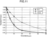
- FIG. 11 is a chart illustrating a relationship between a thickness of a reaction material and a transmittance of thermal neutrons, with a vertical axis representing a transmittance and a horizontal axis representing a thickness.
- a length a length in a right and left direction in FIG. 1 and FIG. 2
- adjusting a length of the reaction layer 4 to be about 50 ⁇ m enables the reaction with about 90% of the thermal neutrons.
- the reflection layer 6 with a thickness of 5 ⁇ m or more absorbs the alpha rays 2 coming out in the upper and lower direction in the reaction layer 4 in FIG. 1 and FIG. 2 and hinders light emission in the scintillator layers 5 on upper and lower sides separated by the reflection layers 6. Thereby, a position resolution is improved.
- the reaction layer 4 is formed in a manner to extend along the incident direction of the neutron 1 as described above. Then, since the neutron 1 proceeds not perpendicularly to but nearly horizontally to this reaction layer 4, and in a manner to move on a diagonal line in the inclinedly disposed reaction layer 4, the reaction efficiency can be greatly improved.
- the scintillator array to be used for the neutron detector according to this embodiment makes it possible to greatly improve use efficiency of neutrons and to perform propagation of the light efficiently without diffusing the light. This makes it possible to obtain the scintillator array to be used for the neutron detector which detects the neutrons efficiently and is capable of imaging with high definition.
- the scintillator array of this embodiment has a reflection layer 6 having a thickness of 5 ⁇ m or more, a reaction layer 4, and a vapor deposition film 7 with a thickness of about 0.1 ⁇ m to 0.5 ⁇ m in a manner to extend along a neutron incident surface (for example, a side surface of a stack) on a neutron incident side (a left side in FIG. 6 ).
- a neutron incident surface for example, a side surface of a stack
- a neutron incident side for example, a side surface of a stack
- a neutron incident side for example, a side surface of a stack
- the explanation of the above-described reflection layer 6, reaction layer 4, and vapor deposition film 7 can be appropriately employed.
- the same reference sign is given to the same portion as that in the embodiment illustrated in FIG. 1 and FIG. 2 , and redundant description is omitted.
- the scintillator array to be used for the neutron detector of the embodiment illustrated in FIG. 6 makes it possible to increase reaction efficiency with a neutron 1 in a neutron input surface in addition to actions and effects in the scintillator illustrated in FIG. 2 . This makes it possible to make a size in a direction (a right and left direction in FIG. 6 ) in which neutrons in the neutron detector are transmitted short and compact.
- a scintillator array to be used for a neutron detector in a case of a plastic scintillator, a glass scintillator not containing hydrogen, a crystal scintillator, or a ceramic scintillator such as a rare earth oxysulfide phosphor or garnet, it is configured such that a scintillator covered by a resin containing hydrogen, or the like, is used for a scintillator layer 5, a vapor deposition film 15 (5 ⁇ m or more in thickness) for absorbing thermal neutrons is provided between the scintillator layer 5 and a reflection layer 6, the vapor deposition film 15 acting as an absorption film absorbing the thermal neutrons, and a vapor deposition film 7 is formed between the vapor deposition film 15 and the scintillator layer 5
- the scintillator array illustrated in FIG. 7 has, on an incident side (left side in FIG. 7 ) of a first neutron 14, a reflection layer 6 of a thickness of 5 ⁇ m or more, a reaction layer 4, and a vapor deposition film 7 of a thickness of about 0.1 ⁇ m to 0.5 ⁇ m for reflection of light in a manner to extend along an incident surface of the fast neutron 14. Since the other portions are configured similarly to the embodiment illustrated in FIG. 1 and FIG. 2 , the same reference sign is given to the corresponding portion and redundant description is omitted.
- the fast neutron 14 being a neutron of a high-energy component reacts in the reaction layer 4, the reaction layer 4 emits an alpha ray 2, the alpha ray 2 reacts in the scintillator layer 5, and the scintillator layer 5 emits light 3.
- a (n, ⁇ ) reaction in the reaction layer 4 when energy of neutrons increases, an absorption cross section declines in the order of digits as indicated by a line of a neutron absorption cross section of enriched boron illustrated in the chart of FIG. 10 which has a vertical axis representing a neutron absorption cross section and a horizontal axis representing neutron energy.
- a reaction probability (efficiency) becomes low. Therefore, it becomes necessary to make a length (a length in a right and left direction in FIG. 7 ) of the reaction layer 4 longer than that in a case of a thermal neutron by the order of digits.
- the fast neutron 14 is slowed down by hydrogen or the like by using the scintillator 5.
- the neutrons 1 generated as a result of slow-down of the fast neutrons 14 are diffused in an isotropic direction from the scintillator layer 5.
- the neutron 1 reacts in the reaction layer 4, the alpha ray 2 is emitted, and this alpha ray 2 reacts with the scintillator layer 5 to generate light 3.
- the neutron 1 slowed down from the fast neutron 14 reacts in the reaction film 4 on an upper side of the scintillator layer 5, emission occurs in the upper and lower scintillator layer 5 to emit the light 3, resulting in the poor resolution.
- the vapor deposition film 15 which includes gadolinium (Gd) having a large absorption cross section in a thermal neutron region on the reflection layer 6 so that the reaction with the reaction layer 4 on the upper side of the scintillator layer 5 does not occur, a wraparound of the neutrons on the lower side can be prevented.
- the neutron 1 generated as a result that the fast neutron 14 is slowed down by a hydrogen atom of the scintillator layer 5 is made to react with the reaction layer 4.
- the range of the neutron 1 is several centimeters or more and diffusion occurs, and thus, by forming the vapor deposition film 15 (whose thickness is 5 ⁇ m to several tens ⁇ m) on one side (lower side in FIG. 7 ) of the reflection layer 6, the neutrons 1 slowed down from the fast neutrons 14 which are diffused are absorbed. This makes it possible to improve the resolution of the detector while increasing the detection efficiency.
- the vapor deposition film 7 is formed for reflection of light.
Landscapes
- Physics & Mathematics (AREA)
- High Energy & Nuclear Physics (AREA)
- Engineering & Computer Science (AREA)
- General Engineering & Computer Science (AREA)
- Health & Medical Sciences (AREA)
- Life Sciences & Earth Sciences (AREA)
- General Physics & Mathematics (AREA)
- Molecular Biology (AREA)
- Spectroscopy & Molecular Physics (AREA)
- Measurement Of Radiation (AREA)
- Conversion Of X-Rays Into Visible Images (AREA)
Applications Claiming Priority (2)
| Application Number | Priority Date | Filing Date | Title |
|---|---|---|---|
| JP2016076704 | 2016-04-06 | ||
| PCT/JP2017/014095 WO2017175763A1 (fr) | 2016-04-06 | 2017-04-04 | Réseau de scintillateurs |
Publications (3)
| Publication Number | Publication Date |
|---|---|
| EP3441793A1 true EP3441793A1 (fr) | 2019-02-13 |
| EP3441793A4 EP3441793A4 (fr) | 2019-11-13 |
| EP3441793B1 EP3441793B1 (fr) | 2025-03-26 |
Family
ID=60001296
Family Applications (1)
| Application Number | Title | Priority Date | Filing Date |
|---|---|---|---|
| EP17779141.5A Active EP3441793B1 (fr) | 2016-04-06 | 2017-04-04 | Réseau de scintillateurs |
Country Status (3)
| Country | Link |
|---|---|
| EP (1) | EP3441793B1 (fr) |
| JP (1) | JP6862427B2 (fr) |
| WO (1) | WO2017175763A1 (fr) |
Cited By (1)
| Publication number | Priority date | Publication date | Assignee | Title |
|---|---|---|---|---|
| US11493648B2 (en) | 2018-10-12 | 2022-11-08 | Hitachi, Ltd. | Radiation monitor and method for measuring radiation |
Families Citing this family (2)
| Publication number | Priority date | Publication date | Assignee | Title |
|---|---|---|---|---|
| JP7063769B2 (ja) * | 2018-08-21 | 2022-05-09 | 株式会社日立製作所 | 放射線モニタ |
| PL3908856T3 (pl) | 2019-01-08 | 2025-09-08 | The Research Foundation For The State University Of New York | Światłowód pryzmatoidowy |
Family Cites Families (8)
| Publication number | Priority date | Publication date | Assignee | Title |
|---|---|---|---|---|
| KR101124549B1 (ko) | 2007-04-24 | 2012-03-20 | 가부시끼가이샤 도시바 | 라디오그래피 측정 장치 및 라디오그래피 측정 방법 |
| RU2502088C2 (ru) * | 2009-07-27 | 2013-12-20 | Флир Радиацион Гмбх | Устройство и способ для детектирования нейтронов посредством калориметрии на основе гамма-захвата |
| JP2010181412A (ja) * | 2010-03-15 | 2010-08-19 | Toshiba Corp | 放射線弁別測定方法および放射線弁別測定装置 |
| JP5710352B2 (ja) * | 2011-04-15 | 2015-04-30 | 株式会社東芝 | 中性子検出器 |
| CN103185894B (zh) * | 2011-12-28 | 2016-08-03 | 同方威视技术股份有限公司 | 一种快中子探测器 |
| MX350345B (es) * | 2012-02-04 | 2017-09-05 | Rapiscan Systems Inc | Sistema de detección de composición de neutrones y rayos gamma. |
| ITRM20130254A1 (it) * | 2013-04-29 | 2014-10-30 | Infn Istituto Naz Di Fisica N Ucleare | "rivelatori di neutroni termici non facenti uso di 3he e metodo per la loro realizzazione" |
| RU2670919C9 (ru) * | 2014-05-01 | 2018-12-12 | Тохоку Техно Арч Ко., Лтд. | Люминофор и детектор излучения |
-
2017
- 2017-04-04 EP EP17779141.5A patent/EP3441793B1/fr active Active
- 2017-04-04 JP JP2018510617A patent/JP6862427B2/ja active Active
- 2017-04-04 WO PCT/JP2017/014095 patent/WO2017175763A1/fr not_active Ceased
Cited By (1)
| Publication number | Priority date | Publication date | Assignee | Title |
|---|---|---|---|---|
| US11493648B2 (en) | 2018-10-12 | 2022-11-08 | Hitachi, Ltd. | Radiation monitor and method for measuring radiation |
Also Published As
| Publication number | Publication date |
|---|---|
| JPWO2017175763A1 (ja) | 2019-02-14 |
| WO2017175763A1 (fr) | 2017-10-12 |
| JP6862427B2 (ja) | 2021-04-21 |
| EP3441793B1 (fr) | 2025-03-26 |
| EP3441793A4 (fr) | 2019-11-13 |
Similar Documents
| Publication | Publication Date | Title |
|---|---|---|
| EP3351971B1 (fr) | Réseau scintillant | |
| McGregor | Materials for gamma-ray spectrometers: Inorganic scintillators | |
| Yanagida | Inorganic scintillating materials and scintillation detectors | |
| US7582880B2 (en) | Neutron detector using lithiated glass-scintillating particle composite | |
| US9121952B2 (en) | Scintillators and applications thereof | |
| JP5710352B2 (ja) | 中性子検出器 | |
| CN1892252A (zh) | 伽马和中子辐射检测器 | |
| Hu et al. | Ultrafast inorganic scintillators for gigahertz hard X-ray imaging | |
| US8399849B1 (en) | Fast neutron detector | |
| JPWO2015190444A1 (ja) | 中性子シンチレーター及び中性子検出器 | |
| EP3441793B1 (fr) | Réseau de scintillateurs | |
| CN114236599B (zh) | 中子探测器及中子探测方法 | |
| JP2006328397A (ja) | 蛍光混和材、蛍光スクリーン及びイメージング組立体 | |
| CN111081728B (zh) | X射线平板探测器及制备方法 | |
| JP2008051626A (ja) | ラインセンサ、ラインセンサユニット及び放射線非破壊検査システム | |
| JP6456946B2 (ja) | 結像システムへの適用のためのCe3+活性化発光組成物 | |
| WO2014188458A1 (fr) | Détecteurs de neutrons thermiques ne faisant pas usage de 3he et procédé pour leur fabrication | |
| US10422888B1 (en) | Scintillation detectors | |
| Korotcenkov et al. | ZnS-Based Neutron and Alpha Radiation Detectors | |
| Batra | Advanced Nuclear Radiation Detectors: Materials, Processing, Properties and Applications | |
| Koroleva et al. | New scintillation materials and scintiblocs for neutron and γ-rays registration | |
| Kuroda et al. | Poissonian-type new radiation imager | |
| JP7117213B2 (ja) | 放射線モニタ及び放射線の測定方法 | |
| JP7691912B2 (ja) | 放射線モニタ、および放射線の検出方法 | |
| Sarkar et al. | Neutron optics and detectors |
Legal Events
| Date | Code | Title | Description |
|---|---|---|---|
| STAA | Information on the status of an ep patent application or granted ep patent |
Free format text: STATUS: THE INTERNATIONAL PUBLICATION HAS BEEN MADE |
|
| PUAI | Public reference made under article 153(3) epc to a published international application that has entered the european phase |
Free format text: ORIGINAL CODE: 0009012 |
|
| STAA | Information on the status of an ep patent application or granted ep patent |
Free format text: STATUS: REQUEST FOR EXAMINATION WAS MADE |
|
| 17P | Request for examination filed |
Effective date: 20181106 |
|
| AK | Designated contracting states |
Kind code of ref document: A1 Designated state(s): AL AT BE BG CH CY CZ DE DK EE ES FI FR GB GR HR HU IE IS IT LI LT LU LV MC MK MT NL NO PL PT RO RS SE SI SK SM TR |
|
| AX | Request for extension of the european patent |
Extension state: BA ME |
|
| DAV | Request for validation of the european patent (deleted) | ||
| DAX | Request for extension of the european patent (deleted) | ||
| A4 | Supplementary search report drawn up and despatched |
Effective date: 20191016 |
|
| RIC1 | Information provided on ipc code assigned before grant |
Ipc: G01T 1/20 20060101ALI20191010BHEP Ipc: G21K 4/00 20060101ALI20191010BHEP Ipc: G01T 3/06 20060101AFI20191010BHEP |
|
| STAA | Information on the status of an ep patent application or granted ep patent |
Free format text: STATUS: EXAMINATION IS IN PROGRESS |
|
| 17Q | First examination report despatched |
Effective date: 20211116 |
|
| GRAP | Despatch of communication of intention to grant a patent |
Free format text: ORIGINAL CODE: EPIDOSNIGR1 |
|
| STAA | Information on the status of an ep patent application or granted ep patent |
Free format text: STATUS: GRANT OF PATENT IS INTENDED |
|
| INTG | Intention to grant announced |
Effective date: 20241016 |
|
| RIN1 | Information on inventor provided before grant (corrected) |
Inventor name: NITTOH, KOICHI Inventor name: NAKASHIMA, NOBUAKI Inventor name: ADACHI, YOSHITAKA Inventor name: FUKUTA, YUKIHIRO |
|
| GRAS | Grant fee paid |
Free format text: ORIGINAL CODE: EPIDOSNIGR3 |
|
| GRAA | (expected) grant |
Free format text: ORIGINAL CODE: 0009210 |
|
| STAA | Information on the status of an ep patent application or granted ep patent |
Free format text: STATUS: THE PATENT HAS BEEN GRANTED |
|
| AK | Designated contracting states |
Kind code of ref document: B1 Designated state(s): AL AT BE BG CH CY CZ DE DK EE ES FI FR GB GR HR HU IE IS IT LI LT LU LV MC MK MT NL NO PL PT RO RS SE SI SK SM TR |
|
| REG | Reference to a national code |
Ref country code: GB Ref legal event code: FG4D |
|
| REG | Reference to a national code |
Ref country code: CH Ref legal event code: EP |
|
| REG | Reference to a national code |
Ref country code: DE Ref legal event code: R096 Ref document number: 602017088534 Country of ref document: DE |
|
| REG | Reference to a national code |
Ref country code: IE Ref legal event code: FG4D |
|
| PG25 | Lapsed in a contracting state [announced via postgrant information from national office to epo] |
Ref country code: RS Free format text: LAPSE BECAUSE OF FAILURE TO SUBMIT A TRANSLATION OF THE DESCRIPTION OR TO PAY THE FEE WITHIN THE PRESCRIBED TIME-LIMIT Effective date: 20250626 |
|
| PG25 | Lapsed in a contracting state [announced via postgrant information from national office to epo] |
Ref country code: FI Free format text: LAPSE BECAUSE OF FAILURE TO SUBMIT A TRANSLATION OF THE DESCRIPTION OR TO PAY THE FEE WITHIN THE PRESCRIBED TIME-LIMIT Effective date: 20250326 |
|
| PGFP | Annual fee paid to national office [announced via postgrant information from national office to epo] |
Ref country code: DE Payment date: 20250402 Year of fee payment: 9 |
|
| REG | Reference to a national code |
Ref country code: LT Ref legal event code: MG9D |
|
| PG25 | Lapsed in a contracting state [announced via postgrant information from national office to epo] |
Ref country code: NO Free format text: LAPSE BECAUSE OF FAILURE TO SUBMIT A TRANSLATION OF THE DESCRIPTION OR TO PAY THE FEE WITHIN THE PRESCRIBED TIME-LIMIT Effective date: 20250626 |
|
| PG25 | Lapsed in a contracting state [announced via postgrant information from national office to epo] |
Ref country code: HR Free format text: LAPSE BECAUSE OF FAILURE TO SUBMIT A TRANSLATION OF THE DESCRIPTION OR TO PAY THE FEE WITHIN THE PRESCRIBED TIME-LIMIT Effective date: 20250326 |
|
| PG25 | Lapsed in a contracting state [announced via postgrant information from national office to epo] |
Ref country code: LV Free format text: LAPSE BECAUSE OF FAILURE TO SUBMIT A TRANSLATION OF THE DESCRIPTION OR TO PAY THE FEE WITHIN THE PRESCRIBED TIME-LIMIT Effective date: 20250326 |
|
| PG25 | Lapsed in a contracting state [announced via postgrant information from national office to epo] |
Ref country code: BG Free format text: LAPSE BECAUSE OF FAILURE TO SUBMIT A TRANSLATION OF THE DESCRIPTION OR TO PAY THE FEE WITHIN THE PRESCRIBED TIME-LIMIT Effective date: 20250326 Ref country code: GR Free format text: LAPSE BECAUSE OF FAILURE TO SUBMIT A TRANSLATION OF THE DESCRIPTION OR TO PAY THE FEE WITHIN THE PRESCRIBED TIME-LIMIT Effective date: 20250627 |
|
| REG | Reference to a national code |
Ref country code: NL Ref legal event code: MP Effective date: 20250326 |
|
| PG25 | Lapsed in a contracting state [announced via postgrant information from national office to epo] |
Ref country code: NL Free format text: LAPSE BECAUSE OF FAILURE TO SUBMIT A TRANSLATION OF THE DESCRIPTION OR TO PAY THE FEE WITHIN THE PRESCRIBED TIME-LIMIT Effective date: 20250326 |
|
| PG25 | Lapsed in a contracting state [announced via postgrant information from national office to epo] |
Ref country code: SE Free format text: LAPSE BECAUSE OF FAILURE TO SUBMIT A TRANSLATION OF THE DESCRIPTION OR TO PAY THE FEE WITHIN THE PRESCRIBED TIME-LIMIT Effective date: 20250326 |
|
| REG | Reference to a national code |
Ref country code: AT Ref legal event code: MK05 Ref document number: 1779469 Country of ref document: AT Kind code of ref document: T Effective date: 20250326 |
|
| PG25 | Lapsed in a contracting state [announced via postgrant information from national office to epo] |
Ref country code: SM Free format text: LAPSE BECAUSE OF FAILURE TO SUBMIT A TRANSLATION OF THE DESCRIPTION OR TO PAY THE FEE WITHIN THE PRESCRIBED TIME-LIMIT Effective date: 20250326 |
|
| PG25 | Lapsed in a contracting state [announced via postgrant information from national office to epo] |
Ref country code: PT Free format text: LAPSE BECAUSE OF FAILURE TO SUBMIT A TRANSLATION OF THE DESCRIPTION OR TO PAY THE FEE WITHIN THE PRESCRIBED TIME-LIMIT Effective date: 20250728 Ref country code: ES Free format text: LAPSE BECAUSE OF FAILURE TO SUBMIT A TRANSLATION OF THE DESCRIPTION OR TO PAY THE FEE WITHIN THE PRESCRIBED TIME-LIMIT Effective date: 20250326 |
|
| PG25 | Lapsed in a contracting state [announced via postgrant information from national office to epo] |
Ref country code: IT Free format text: LAPSE BECAUSE OF FAILURE TO SUBMIT A TRANSLATION OF THE DESCRIPTION OR TO PAY THE FEE WITHIN THE PRESCRIBED TIME-LIMIT Effective date: 20250326 Ref country code: PL Free format text: LAPSE BECAUSE OF FAILURE TO SUBMIT A TRANSLATION OF THE DESCRIPTION OR TO PAY THE FEE WITHIN THE PRESCRIBED TIME-LIMIT Effective date: 20250326 |
|
| PG25 | Lapsed in a contracting state [announced via postgrant information from national office to epo] |
Ref country code: AT Free format text: LAPSE BECAUSE OF FAILURE TO SUBMIT A TRANSLATION OF THE DESCRIPTION OR TO PAY THE FEE WITHIN THE PRESCRIBED TIME-LIMIT Effective date: 20250326 |
|
| PG25 | Lapsed in a contracting state [announced via postgrant information from national office to epo] |
Ref country code: EE Free format text: LAPSE BECAUSE OF FAILURE TO SUBMIT A TRANSLATION OF THE DESCRIPTION OR TO PAY THE FEE WITHIN THE PRESCRIBED TIME-LIMIT Effective date: 20250326 |
|
| PG25 | Lapsed in a contracting state [announced via postgrant information from national office to epo] |
Ref country code: RO Free format text: LAPSE BECAUSE OF FAILURE TO SUBMIT A TRANSLATION OF THE DESCRIPTION OR TO PAY THE FEE WITHIN THE PRESCRIBED TIME-LIMIT Effective date: 20250326 |
|
| PG25 | Lapsed in a contracting state [announced via postgrant information from national office to epo] |
Ref country code: SK Free format text: LAPSE BECAUSE OF FAILURE TO SUBMIT A TRANSLATION OF THE DESCRIPTION OR TO PAY THE FEE WITHIN THE PRESCRIBED TIME-LIMIT Effective date: 20250326 |
|
| PG25 | Lapsed in a contracting state [announced via postgrant information from national office to epo] |
Ref country code: IS Free format text: LAPSE BECAUSE OF FAILURE TO SUBMIT A TRANSLATION OF THE DESCRIPTION OR TO PAY THE FEE WITHIN THE PRESCRIBED TIME-LIMIT Effective date: 20250726 |
|
| REG | Reference to a national code |
Ref country code: CH Ref legal event code: H13 Free format text: ST27 STATUS EVENT CODE: U-0-0-H10-H13 (AS PROVIDED BY THE NATIONAL OFFICE) Effective date: 20251125 |
|
| PG25 | Lapsed in a contracting state [announced via postgrant information from national office to epo] |
Ref country code: LU Free format text: LAPSE BECAUSE OF NON-PAYMENT OF DUE FEES Effective date: 20250404 |
|
| PG25 | Lapsed in a contracting state [announced via postgrant information from national office to epo] |
Ref country code: MC Free format text: LAPSE BECAUSE OF FAILURE TO SUBMIT A TRANSLATION OF THE DESCRIPTION OR TO PAY THE FEE WITHIN THE PRESCRIBED TIME-LIMIT Effective date: 20250326 |
|
| REG | Reference to a national code |
Ref country code: BE Ref legal event code: MM Effective date: 20250430 |
|
| REG | Reference to a national code |
Ref country code: DE Ref legal event code: R097 Ref document number: 602017088534 Country of ref document: DE |
|
| PG25 | Lapsed in a contracting state [announced via postgrant information from national office to epo] |
Ref country code: DK Free format text: LAPSE BECAUSE OF FAILURE TO SUBMIT A TRANSLATION OF THE DESCRIPTION OR TO PAY THE FEE WITHIN THE PRESCRIBED TIME-LIMIT Effective date: 20250326 |
|
| PG25 | Lapsed in a contracting state [announced via postgrant information from national office to epo] |
Ref country code: BE Free format text: LAPSE BECAUSE OF NON-PAYMENT OF DUE FEES Effective date: 20250430 |
|
| PG25 | Lapsed in a contracting state [announced via postgrant information from national office to epo] |
Ref country code: CH Free format text: LAPSE BECAUSE OF NON-PAYMENT OF DUE FEES Effective date: 20250430 |
|
| PG25 | Lapsed in a contracting state [announced via postgrant information from national office to epo] |
Ref country code: CZ Free format text: LAPSE BECAUSE OF FAILURE TO SUBMIT A TRANSLATION OF THE DESCRIPTION OR TO PAY THE FEE WITHIN THE PRESCRIBED TIME-LIMIT Effective date: 20250326 |
|
| PLBE | No opposition filed within time limit |
Free format text: ORIGINAL CODE: 0009261 |
|
| STAA | Information on the status of an ep patent application or granted ep patent |
Free format text: STATUS: NO OPPOSITION FILED WITHIN TIME LIMIT |
|
| REG | Reference to a national code |
Ref country code: CH Ref legal event code: L10 Free format text: ST27 STATUS EVENT CODE: U-0-0-L10-L00 (AS PROVIDED BY THE NATIONAL OFFICE) Effective date: 20260211 |
|
| 26N | No opposition filed |
Effective date: 20260105 |
|
| PGFP | Annual fee paid to national office [announced via postgrant information from national office to epo] |
Ref country code: GB Payment date: 20260303 Year of fee payment: 10 |
|
| PG25 | Lapsed in a contracting state [announced via postgrant information from national office to epo] |
Ref country code: IE Free format text: LAPSE BECAUSE OF NON-PAYMENT OF DUE FEES Effective date: 20250404 |
|
| PGFP | Annual fee paid to national office [announced via postgrant information from national office to epo] |
Ref country code: FR Payment date: 20260223 Year of fee payment: 10 |