EP3442015B1 - Waferhaltemechanismus und verfahren für drehtisch und drehwaferhaltevorrichtung - Google Patents
Waferhaltemechanismus und verfahren für drehtisch und drehwaferhaltevorrichtung Download PDFInfo
- Publication number
- EP3442015B1 EP3442015B1 EP17802674.6A EP17802674A EP3442015B1 EP 3442015 B1 EP3442015 B1 EP 3442015B1 EP 17802674 A EP17802674 A EP 17802674A EP 3442015 B1 EP3442015 B1 EP 3442015B1
- Authority
- EP
- European Patent Office
- Prior art keywords
- wafer
- outer peripheral
- holding
- columnar
- movable outer
- Prior art date
- Legal status (The legal status is an assumption and is not a legal conclusion. Google has not performed a legal analysis and makes no representation as to the accuracy of the status listed.)
- Active
Links
Images
Classifications
-
- H—ELECTRICITY
- H10—SEMICONDUCTOR DEVICES; ELECTRIC SOLID-STATE DEVICES NOT OTHERWISE PROVIDED FOR
- H10P—GENERIC PROCESSES OR APPARATUS FOR THE MANUFACTURE OR TREATMENT OF DEVICES COVERED BY CLASS H10
- H10P72/00—Handling or holding of wafers, substrates or devices during manufacture or treatment thereof
- H10P72/70—Handling or holding of wafers, substrates or devices during manufacture or treatment thereof for supporting or gripping
- H10P72/76—Handling or holding of wafers, substrates or devices during manufacture or treatment thereof for supporting or gripping using mechanical means, e.g. clamps or pinches
- H10P72/7604—Handling or holding of wafers, substrates or devices during manufacture or treatment thereof for supporting or gripping using mechanical means, e.g. clamps or pinches the wafers being placed on a susceptor, stage or support
- H10P72/7614—Handling or holding of wafers, substrates or devices during manufacture or treatment thereof for supporting or gripping using mechanical means, e.g. clamps or pinches the wafers being placed on a susceptor, stage or support characterised by a plurality of individual support members, e.g. support posts or protrusions
-
- H—ELECTRICITY
- H10—SEMICONDUCTOR DEVICES; ELECTRIC SOLID-STATE DEVICES NOT OTHERWISE PROVIDED FOR
- H10P—GENERIC PROCESSES OR APPARATUS FOR THE MANUFACTURE OR TREATMENT OF DEVICES COVERED BY CLASS H10
- H10P50/00—Etching of wafers, substrates or parts of devices
-
- H—ELECTRICITY
- H10—SEMICONDUCTOR DEVICES; ELECTRIC SOLID-STATE DEVICES NOT OTHERWISE PROVIDED FOR
- H10P—GENERIC PROCESSES OR APPARATUS FOR THE MANUFACTURE OR TREATMENT OF DEVICES COVERED BY CLASS H10
- H10P52/00—Grinding, lapping or polishing of wafers, substrates or parts of devices
-
- H—ELECTRICITY
- H10—SEMICONDUCTOR DEVICES; ELECTRIC SOLID-STATE DEVICES NOT OTHERWISE PROVIDED FOR
- H10P—GENERIC PROCESSES OR APPARATUS FOR THE MANUFACTURE OR TREATMENT OF DEVICES COVERED BY CLASS H10
- H10P72/00—Handling or holding of wafers, substrates or devices during manufacture or treatment thereof
- H10P72/70—Handling or holding of wafers, substrates or devices during manufacture or treatment thereof for supporting or gripping
- H10P72/76—Handling or holding of wafers, substrates or devices during manufacture or treatment thereof for supporting or gripping using mechanical means, e.g. clamps or pinches
- H10P72/7604—Handling or holding of wafers, substrates or devices during manufacture or treatment thereof for supporting or gripping using mechanical means, e.g. clamps or pinches the wafers being placed on a susceptor, stage or support
- H10P72/7608—Handling or holding of wafers, substrates or devices during manufacture or treatment thereof for supporting or gripping using mechanical means, e.g. clamps or pinches the wafers being placed on a susceptor, stage or support characterised by a plurality of separate clamping members, e.g. clamping fingers
-
- H—ELECTRICITY
- H10—SEMICONDUCTOR DEVICES; ELECTRIC SOLID-STATE DEVICES NOT OTHERWISE PROVIDED FOR
- H10P—GENERIC PROCESSES OR APPARATUS FOR THE MANUFACTURE OR TREATMENT OF DEVICES COVERED BY CLASS H10
- H10P76/00—Manufacture or treatment of masks on semiconductor bodies, e.g. by lithography or photolithography
Definitions
- the present invention relates to a wafer holding mechanism for a rotary table and a method in a wafer rotating and holding device, and to a wafer rotating and holding device.
- spin processes in semiconductor manufacturing processes, there are an increasing number of steps (also called “spin processes") in which various kinds of processing are performed while a semiconductor wafer made of, for example, silicon is rotated, such as spin etching, spin drying, and spin coating.
- steps also called “spin processes”
- wafer rotating and holding devices such as a spin etching device, a spin drying device, and a spin coating device.
- processing to be performed on a wafer surface in manufacturing processes for a device there can be given, in addition to etching processing for removing a damaged layer after back-grinding, applying developer to the wafer, developing processing on the wafer, which has a surface that has circuit patterns exposed thereon and is applied with developer, and which is printed with a semiconductor circuit, cleaning the wafer surface, and the like.
- a wafer rotating and holding device and method used for performing spin processing on a wafer there are given, for example, devices and methods described in Patent Documents 1 to 4.
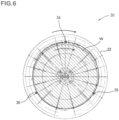
- FIG. 5 is a schematic diagram for illustrating a wafer rotating and holding device of the related art
- FIG. 6 is an enlarged view of a main part for illustrating details of a driver of FIG. 5
- a wafer W on a rotary table 32 in a wafer rotating and holding device 30 of the related art is held by three outer peripheral pins made up of one movable pin 34 and two fixed pins 36.
- Support pins for supporting a lower surface of the wafer W are each denoted by a reference symbol 40 in FIG. 5 .
- the movable pin 34 When the wafer W is loaded, the movable pin 34 is opened outward to set the wafer W and is then closed, thereby pressing the wafer W toward the fixed pins 36 to hold the wafer W. Once the wafer W is held, spin processing is performed under this state and, after the spin processing is completed, the wafer W is taken out by opening the movable pin 34. A force to drive the movable pin 34 is transmitted from the outside while the spin is stopped, and a cylinder 38 mounted to a non-rotary structure is pushed up to open/close the movable pin 34. During the spin processing, the movable pin 34, which has a hinged structure, presses the wafer W toward the fixed pins 36 with a spring at a pressure that is kept constant throughout the duration of the spin processing to hold the wafer W.
- Patent document 5 discloses a wafer rotating and holding device that enables the rotation-type holding members to be driven in a simple configuration by utilizing the electrical action and the magnetic action without using a mechanical drive mechanism. In this document, the mechanical drive mechanism has been eliminated from the rotating mechanism.
- the present invention has been made in view of the related art described above, and an object of the present invention is to provide a wafer holding mechanism for a rotary table and a method, and a wafer rotating and holding device, which enable change of holding positions of the wafer during spin processing while maintaining the posture of the wafer, enable reduction of marks of outer peripheral pins due to etching, and enable reduction of insufficient cleaning or uneven cleaning, by using a plurality of movable outer peripheral pins and switching the movable outer peripheral pins which hold the wafer.
- a wafer holding mechanism for a rotary table is as follows:
- a wafer holding method for a rotary table according of the present invention comprises using the above-mentioned wafer holding mechanism for the rotary table to hold the wafer.
- a wafer rotating and holding device comprises the above-mentioned wafer holding mechanism for the rotary table.
- the wafer rotating and holding device further comprises any one of a mechanism for performing spin etching, spin drying, spin coating, a mechanism for performing on a wafer surface manufacturing processes for a device, a mechanism for removing a damaged layer after back-grinding, a mechanism for applying developer to the wafer, a mechanism for performing developing processing on the wafer which has a surface that has circuit patterns exposed thereon and is applied with developer and which is printed with a semiconductor circuit, and a mechanism for cleaning the wafer surface.
- a mechanism for performing spin etching, spin drying, spin coating a mechanism for performing on a wafer surface manufacturing processes for a device, a mechanism for removing a damaged layer after back-grinding, a mechanism for applying developer to the wafer, a mechanism for performing developing processing on the wafer which has a surface that has circuit patterns exposed thereon and is applied with developer and which is printed with a semiconductor circuit, and a mechanism for cleaning the wafer surface.
- the wafer holding mechanism for the rotary table and the method, and the wafer rotating and holding device which enable change of holding positions of the wafer during spin processing while maintaining the posture of the wafer, enable reduction of marks of outer peripheral pins due to etching, and enable reduction of insufficient cleaning or uneven cleaning, by using a plurality of movable outer peripheral pins and switching the movable outer peripheral pins which hold the wafer.
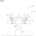
- a wafer holding mechanism for a rotary table according to the present invention is denoted by a reference symbol 10 in FIG. 1 and FIG. 2 .
- the wafer holding mechanism 10 for the rotary table is a wafer holding mechanism for a rotary table of a wafer rotating and holding device 11, and comprises: a rotary shaft 18; a rotary table 12 placed on an end of the rotary shaft 18 and configured to hold a wafer W on an upper surface of the rotary table 12; a drive motor 20 configured to supply motive power to the rotary shaft 18; and a plurality of movable outer peripheral pins provided in the rotary table 12 and configured to hold an outer periphery of the wafer.
- the plurality of movable outer peripheral pins comprise: a plurality of first movable outer peripheral pins 14; and a plurality of second movable outer peripheral pins 16, which are configured to hold the wafer W at positions different from holding positions of the wafer W by the plurality of first movable outer peripheral pins 14.
- the second movable outer peripheral pins 16 are configured to avoid holding the wafer W during a period in which the first movable outer peripheral pins 14 are holding the wafer W
- the first movable outer peripheral pins 14 are configured to avoid holding the wafer W during a period in which the second movable outer peripheral pins 16 are holding the wafer W
- holding positions of the wafer W are changed by switching holding by the first movable outer peripheral pins 14 and the second movable outer peripheral pins 16 during processing of the wafer W.
- support pins for supporting a lower surface of the wafer W are each denoted by a reference symbol 24.
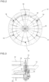
- FIG. 2 is a plan view for illustrating details of a driver in an example of the wafer rotating and holding device 11, which comprises the wafer holding mechanism 10 for the rotary table according to the present invention.
- three first movable outer peripheral pins 14, which can be moved by approximately 2 mm in an outward radial direction of the wafer W, and three second movable outer peripheral pins 16, which can be moved by approximately 2 mm in the outward radial direction, are used as the plurality of movable outer peripheral pins.
- the first movable outer peripheral pins 14 and the second movable outer peripheral pins 16 alternate in holding the wafer W during wafer processing, to thereby change holding positions of the wafer W during spin processing while maintaining the posture of the wafer W. This lessens marks of the outer peripheral pins left by etching, and reduces insufficient cleaning or cleaning unevenness.
- a permanent magnet is denoted by a reference symbol 22 and a fulcrum is denoted by a reference symbol 26 in FIG. 1 and FIG. 3 .
- the permanent magnet 22 is embedded below a wafer lever to use a lever method in which the wafer lever opens or closes depending on whether the magnetic force of the electromagnet is strong or weak, and which of the first movable outer peripheral pins 14 and the second movable outer peripheral pins 16 hold the wafer is switched by changing the polarity of the electromagnet.
- the second movable outer peripheral pins 16 are pulled down in the inward radial direction to be ready for wafer holding, and then the first movable outer peripheral pins 14 are pulled down in the outward radial direction to stop holding the wafer W and to let the second movable outer peripheral pins 16 hold the wafer W.
- the first movable outer peripheral pins 14 and the second movable outer peripheral pins 16 are alternated to change positions at which the wafer is held.
- a pressure at which the pins are pressed to the wafer may be controlled by changing a voltage applied to the solenoid.
- the rotary shaft 18 is made of stainless steel (SUS), and the rotary table 12 is made of industrial plastic or other types of synthetic resin.
- the number of revolutions of the rotary table 12 is not particularly limited, but 100 rpm to 1,000 rpm is preferred.
- the shape of the first movable outer peripheral pins 14 and the second movable outer peripheral pins 16 is not particularly limited, but a columnar shape is preferred.
- the pins in the illustrated example each have a columnar shape that is approximately 3 mm in diameter.
- a plurality of first movable outer peripheral pins 14 and a plurality of second movable outer peripheral pins 16 are provided, and three or more first movable outer peripheral pins 14 and three or more second movable outer peripheral pins 16 are desired to be provided.
- the first movable outer peripheral pins 14 and the second movable outer peripheral pins 16 are desired to be arranged evenly. It is preferred in the present invention that all outer peripheral pins for holding the outer periphery of a wafer be movable.
- How electric power is supplied to drive the solenoid is not limited to a particular method, and methods that can be used are, for example, one in which electric power is supplied from a battery embedded in the rotary table and motor driving is switched with a centrifugal force obtained by rotating the rotary table, one in which electric power is supplied from the rotary shaft by utilizing a slip ring to start rotation at the same time as electric power feeding, and one in which electric power is supplied to the rotary table with the use of electromagnetic induction to start rotation at the same time as electric power feeding.
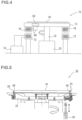
- An electric power supply mechanism 70 is illustrated in FIG. 4 as a mode of carrying out electric power supply means that uses the method of using the electromagnetic induction.
- the electric power supply mechanism 70 in FIG. 4 comprises: the rotary shaft 18; the rotary table 12 placed on an end of the rotary shaft 18 and configured to hold the wafer W on the upper surface of the rotary table 12; the drive motor 20 configured to supply motive power to the rotary shaft 18; a fixed-side primary coil 72 wound around the rotary shaft 18; an electric power supply source 74 connected to the fixed-side primary coil 72; and a rotary table-side secondary coil 76, which is provided so as to correspond to the fixed-side primary coil 72 and be separated from the fixed-side primary coil 72 by a predetermined distance, and is mounted to the rotary table 12.
- a rotation control motor is connected to the rotary table-side secondary coil 76 via electric wires 80 so that electric power is supplied to a load 50 of the solenoid and of others by electromagnetic induction via the secondary coil 76.
- the wafer rotating and holding device comprises a spin processing mechanism.
- the spin processing mechanism is, for example, an etching processing mechanism in a spin etching device, a drying mechanism in a spin drying device, or a coating mechanism in a spin coating device.
- spin processing mechanisms there can be given, as processing to be performed on a wafer surface in manufacturing processes for a device, in addition to the etching processing mechanism for removing a damaged layer after back-grinding, a mechanism for applying developer to the wafer, a mechanism for performing developing processing on the wafer, which has a surface that has circuit patterns exposed thereon and is applied with developer, and which is printed with a semiconductor circuit, and a mechanism for cleaning the wafer surface, and the like.
- Chemical solutions to be used in the processing are not particularly limited, and acid-based/alkaline-based etching cleaning liquids and rinse water can be suitably used.
- a wafer holding method for a rotary table according to the present invention is a method of holding a wafer with the use of the wafer holding mechanism for the rotary table.
- the wafer rotating and holding device is a device comprising the wafer holding mechanism for the rotary table.
- 10 wafer holding mechanism for rotary table according to the present invention
- 11 wafer rotating and holding device according to the present invention
- 12 rotary table
- 14 first movable outer peripheral pin
- 16 second movable outer peripheral pin
- 18 rotary shaft
- 20 drive motor
- 22 permanent magnet
- 24, 40 support pin
- 26 fulcrum
- 28 solenoid
- 30 wafer rotating and holding device of the related art
- 34 movable pin
- 36 fixed pin
- 38 cylinder
- 50 load
- 70 electric power supply mechanism
- 72 fixed-side primary coil
- 74 electric power supply source
- 76 rotary table-side secondary coil
- W wafer.
Landscapes
- Cleaning Or Drying Semiconductors (AREA)
- Container, Conveyance, Adherence, Positioning, Of Wafer (AREA)
- Exposure Of Semiconductors, Excluding Electron Or Ion Beam Exposure (AREA)
Claims (4)
- Wafer-Haltemechanismus einer Wafer-Dreh- und Haltevorrichtung (11), wobei der Wafer-Haltemechanismus umfasst:eine rotierende Welle (18);einen Drehtisch (12, 32), der an einem Ende der rotierenden Welle (18) angeordnet und so konfiguriert ist, dass er einen Wafer (W) auf einer oberen Fläche des Drehtisches (12, 32) hält;eine Vielzahl von säulenförmigen Stützstiften (24, 40) mit einer sich verjüngenden Spitze, die auf dem Drehtisch (12, 32) angeordnet und so konfiguriert sind, dass sie eine untere Fläche des Wafers (W) stützen;einen Antriebsmotor (20), der so konfiguriert ist, dass er die rotierende Welle (18) mit Antriebskraft versorgt;ein Magnetventil (28), das im Inneren des Drehtisches (12, 32) vorgesehen ist,einem Dauermagneten (22), der im Inneren des Drehtisches (12, 32) dem Magneten (28) gegenüberliegt,einen Stromversorgungsmechanismus (70) zum Antreiben der Magnetspule (28); undeine Vielzahl von säulenförmigen beweglichen äußeren Umfangsstiften, die in dem Drehtisch (12, 32) vorgesehen und so konfiguriert sind, dass sie einen äußeren Umfang des Wafers (W) halten,wobei die säulenförmigen beweglichen äußeren Umfangsstifte so konfiguriert sind,dass sie in einer nach innen gerichteten radialen Richtung des Wafers (W) nach unten ziehen, um den Wafer (W) zu halten, oder die säulenförmigen beweglichen äußeren Umfangsstifte so konfiguriert sind, dass sie in der nach außen gerichteten radialen Richtung des Wafers (W) nach unten ziehen, um ein Halten des Wafers (W) zu vermeiden,wobei die Vielzahl von säulenförmigen beweglichen äußeren Umfangsstiften umfasst:eine Vielzahl von säulenförmigen ersten beweglichen äußeren Umfangsstiften (14) undeine Vielzahl von säulenförmigen zweiten beweglichen äußeren Umfangsstiften (16), die so konfiguriert sind, dass sie den Wafer (W) an Positionen halten, die sich von den Haltepositionen des Wafers (W) durch die Vielzahl der säulenförmigen ersten beweglichen äußeren Umfangsstifte (14) unterscheiden,wobei zum Zuführen des Wafers (W) die säulenförmigen ersten beweglichen äußeren Umfangsstifte (14) und die säulenförmigen zweiten beweglichen äußeren Umfangsstifte (16) so konfiguriert sind, dass sie sich in der nach außen gerichteten radialen Richtung nach unten ziehen, um ein Halten des Wafers (W) zu vermeiden,wobei die mehreren säulenförmigen zweiten beweglichen äußeren Umfangsstifte (16) so konfiguriert sind, dass sie das Halten des Wafers (W) während eines Zeitraums, in dem die mehreren säulenförmigen ersten beweglichen äußeren Umfangsstifte (14) den Wafer (W) halten, vermeiden, und die mehreren säulenförmigen ersten beweglichen äußeren Umfangsstifte (14) so konfiguriert sind, dass sie das Halten des Wafers (W) während eines Zeitraums, in dem die mehreren säulenförmigen zweiten beweglichen äußeren Umfangsstifte (16) den Wafer (W) halten, vermeiden, nachdem der Wafer (W) eingestellt ist,wobei die Haltepositionen des Wafers (W) so konstruiert sind, dass sie sich durch Umschalten des Haltens durch die säulenförmigen ersten beweglichen äußeren Umfangsstifte (14) und des Haltens durch die säulenförmigen zweiten beweglichen äußeren Umfangsstifte (16) während der Bearbeitung des Wafers (W) ändern,wobei das Halten des Wafers (W) durch die mehreren säulenförmigen beweglichen äußeren Umfangsstifte mit dem Solenoid (28) durch Ändern der Polarität des Solenoids (28) gesteuert wird, um in einer nach innen gerichteten radialen Richtung des Wafers (W) nach unten zu ziehen, um den Wafer (W) zu halten, oder um in der nach außen gerichteten radialen Richtung des Wafers (W) nach unten zu ziehen, um das Halten des Wafers (W) zu vermeiden,und wobei der elektrische Stromversorgungsmechanismus (70) eine feststehende Primärspule (72), die um die rotierende Welle (18) gewickelt ist, und eine rotierende tischseitige Sekundärspule (76) umfasst, die so vorgesehen ist, dass sie mit der feststehenden Primärspule (72) korrespondiert und von der feststehenden Primärspule (72) um einen vorbestimmten Abstand getrennt ist, und die an dem Drehtisch (12, 32) angebracht ist.
- Waferhalteverfahren für einen Drehtisch (12, 32), bei dem der Waferhaltemechanismus nach Anspruch 1 zum Halten des Wafers (W) verwendet wird.
- Wafer-Dreh- und Haltevorrichtung (11), die den Wafer-Haltemechanismus nach Anspruch 1 umfasst.
- Wafer-Dreh- und -Haltevorrichtung (11) nach Anspruch 3, ferner umfassend einen Mechanismus zum Durchführen von Spin-Ätzen, Spin-Trocknen, Spin-Beschichten, einen Mechanismus zum Durchführen von Herstellungsprozessen für eine Vorrichtung auf der Oberfläche eines Wafers (W), einen Mechanismus zum Entfernen einer beschädigten Schicht nach dem Rückschleifen, einen Mechanismus zum Auftragen von Entwickler auf den Wafer (W), einen Mechanismus zum Durchführen eines Entwicklungsprozesses auf dem Wafer (W), der eine Oberfläche aufweist, auf der Schaltungsmuster freigelegt sind und die mit Entwickler aufgetragen ist und die mit einer Halbleiterschaltung bedruckt ist, und einen Mechanismus zum Reinigen der Oberfläche des Wafers (W).
Applications Claiming Priority (2)
| Application Number | Priority Date | Filing Date | Title |
|---|---|---|---|
| JP2016103243 | 2016-05-24 | ||
| PCT/JP2017/018695 WO2017204082A1 (ja) | 2016-05-24 | 2017-05-18 | 回転テーブル用ウェーハ保持機構及び方法並びにウェーハ回転保持装置 |
Publications (3)
| Publication Number | Publication Date |
|---|---|
| EP3442015A1 EP3442015A1 (de) | 2019-02-13 |
| EP3442015A4 EP3442015A4 (de) | 2019-11-13 |
| EP3442015B1 true EP3442015B1 (de) | 2024-02-14 |
Family
ID=60412842
Family Applications (1)
| Application Number | Title | Priority Date | Filing Date |
|---|---|---|---|
| EP17802674.6A Active EP3442015B1 (de) | 2016-05-24 | 2017-05-18 | Waferhaltemechanismus und verfahren für drehtisch und drehwaferhaltevorrichtung |
Country Status (5)
| Country | Link |
|---|---|
| US (1) | US10818538B2 (de) |
| EP (1) | EP3442015B1 (de) |
| JP (1) | JP6634154B2 (de) |
| CN (1) | CN109155272A (de) |
| WO (1) | WO2017204082A1 (de) |
Families Citing this family (6)
| Publication number | Priority date | Publication date | Assignee | Title |
|---|---|---|---|---|
| JP6622389B2 (ja) * | 2016-04-21 | 2019-12-18 | 三益半導体工業株式会社 | 回転テーブル用非接触電力供給機構及び方法並びにウェーハ回転保持装置 |
| JP6634154B2 (ja) * | 2016-05-24 | 2020-01-22 | 三益半導体工業株式会社 | 回転テーブル用ウェーハ保持機構及び方法並びにウェーハ回転保持装置 |
| KR101856875B1 (ko) * | 2016-12-06 | 2018-05-10 | 에스케이실트론 주식회사 | 웨이퍼 캐리어 두께 측정장치 |
| CN111048466B (zh) * | 2019-12-26 | 2022-08-16 | 北京北方华创微电子装备有限公司 | 晶圆夹持装置 |
| JP7619897B2 (ja) * | 2021-06-16 | 2025-01-22 | 株式会社荏原製作所 | 基板支持機構、基板洗浄装置及び基板処理方法 |
| JP7759299B2 (ja) * | 2022-06-22 | 2025-10-23 | 芝浦メカトロニクス株式会社 | 基板処理装置 |
Citations (2)
| Publication number | Priority date | Publication date | Assignee | Title |
|---|---|---|---|---|
| KR100809593B1 (ko) * | 2006-09-12 | 2008-03-04 | 세메스 주식회사 | 스핀헤드 |
| US20100126539A1 (en) * | 2008-11-26 | 2010-05-27 | Semes Co., Ltd. | Spin head, apparatus for treating substrate, and method for treating substrate |
Family Cites Families (21)
| Publication number | Priority date | Publication date | Assignee | Title |
|---|---|---|---|---|
| JPH06232047A (ja) * | 1993-01-29 | 1994-08-19 | Mitsubishi Heavy Ind Ltd | ウェハ回転装置 |
| US5421893A (en) * | 1993-02-26 | 1995-06-06 | Applied Materials, Inc. | Susceptor drive and wafer displacement mechanism |
| US5676360A (en) * | 1995-07-11 | 1997-10-14 | Boucher; John N. | Machine tool rotary table locking apparatus |
| JPH09107023A (ja) | 1995-10-13 | 1997-04-22 | Toshiba Microelectron Corp | 被処理物の回転保持装置 |
| US6190113B1 (en) * | 1997-04-30 | 2001-02-20 | Applied Materials, Inc. | Quartz pin lift for single wafer chemical vapor deposition/etch process chamber |
| JP2000094307A (ja) * | 1998-09-18 | 2000-04-04 | Ebara Corp | ポリッシング装置 |
| US6305677B1 (en) * | 1999-03-30 | 2001-10-23 | Lam Research Corporation | Perimeter wafer lifting |
| JP4257816B2 (ja) | 2000-03-16 | 2009-04-22 | 三益半導体工業株式会社 | 廃液回収機構付ウェーハ表面処理装置 |
| JP4111479B2 (ja) | 1999-09-09 | 2008-07-02 | 三益半導体工業株式会社 | ウェーハ回転保持装置 |
| JP2004115872A (ja) * | 2002-09-26 | 2004-04-15 | Dainippon Screen Mfg Co Ltd | 基板処理装置および基板処理方法 |
| US7018555B2 (en) * | 2002-07-26 | 2006-03-28 | Dainippon Screen Mfg. Co., Ltd. | Substrate treatment method and substrate treatment apparatus |
| JP2004241492A (ja) | 2003-02-04 | 2004-08-26 | Dainippon Screen Mfg Co Ltd | 基板処理装置 |
| US7056392B1 (en) * | 2003-04-16 | 2006-06-06 | Lsi Logic Corporation | Wafer chucking apparatus and method for spin processor |
| JP4364242B2 (ja) | 2004-03-22 | 2009-11-11 | 三益半導体工業株式会社 | スピンエッチングにおける工程管理方法及びスピンエッチング装置 |
| US20090032498A1 (en) | 2005-03-30 | 2009-02-05 | Mimasu Semiconductor Industry Co., Ltd. | Spin Processing Method And Apparatus |
| JP4753832B2 (ja) * | 2006-10-19 | 2011-08-24 | 大日本スクリーン製造株式会社 | 基板回転保持装置および基板処理装置 |
| KR101017654B1 (ko) * | 2008-11-26 | 2011-02-25 | 세메스 주식회사 | 기판 척킹 부재, 이를 갖는 기판 처리 장치 및 이를 이용한기판 처리 방법 |
| JP6053528B2 (ja) * | 2013-01-11 | 2016-12-27 | 株式会社荏原製作所 | 基板把持装置 |
| JP6205159B2 (ja) | 2013-04-09 | 2017-09-27 | 芝浦メカトロニクス株式会社 | 基板把持装置および基板処理装置 |
| JP6302665B2 (ja) * | 2013-12-24 | 2018-03-28 | 株式会社ディスコ | スピンナー装置 |
| JP6634154B2 (ja) * | 2016-05-24 | 2020-01-22 | 三益半導体工業株式会社 | 回転テーブル用ウェーハ保持機構及び方法並びにウェーハ回転保持装置 |
-
2017
- 2017-05-18 JP JP2018519229A patent/JP6634154B2/ja active Active
- 2017-05-18 WO PCT/JP2017/018695 patent/WO2017204082A1/ja not_active Ceased
- 2017-05-18 EP EP17802674.6A patent/EP3442015B1/de active Active
- 2017-05-18 CN CN201780030916.3A patent/CN109155272A/zh active Pending
- 2017-05-18 US US16/302,859 patent/US10818538B2/en active Active
Patent Citations (2)
| Publication number | Priority date | Publication date | Assignee | Title |
|---|---|---|---|---|
| KR100809593B1 (ko) * | 2006-09-12 | 2008-03-04 | 세메스 주식회사 | 스핀헤드 |
| US20100126539A1 (en) * | 2008-11-26 | 2010-05-27 | Semes Co., Ltd. | Spin head, apparatus for treating substrate, and method for treating substrate |
Also Published As
| Publication number | Publication date |
|---|---|
| JP6634154B2 (ja) | 2020-01-22 |
| US10818538B2 (en) | 2020-10-27 |
| US20190295879A1 (en) | 2019-09-26 |
| WO2017204082A1 (ja) | 2017-11-30 |
| JPWO2017204082A1 (ja) | 2019-04-04 |
| CN109155272A (zh) | 2019-01-04 |
| EP3442015A1 (de) | 2019-02-13 |
| EP3442015A4 (de) | 2019-11-13 |
Similar Documents
| Publication | Publication Date | Title |
|---|---|---|
| US10818538B2 (en) | Wafer holding mechanism for rotary table and method and wafer rotating and holding device | |
| EP3442016B1 (de) | Wafererwärmungs- und -haltevorrichtung und -verfahren für drehtisch sowie waferdreh- und -haltevorrichtung | |
| US11031235B2 (en) | Substrate processing apparatus | |
| KR101587359B1 (ko) | 스핀 처리 장치 | |
| CN108630566B (zh) | 基板保持旋转装置及具备该装置的基板处理装置及方法 | |
| US7866058B2 (en) | Spin head and substrate treating method using the same | |
| EP3432351B1 (de) | Mechanismus und verfahren zur kontaktlosen stromversorgung für drehtisch und waferdreh- und -haltevorrichtung | |
| CN109564859A (zh) | 基板处理方法以及基板处理装置 | |
| JP3625264B2 (ja) | 基板処理装置 | |
| JP6715078B2 (ja) | 回転テーブル用ウェーハ保持機構及び方法並びにウェーハ回転保持装置 | |
| KR101099733B1 (ko) | 기판 처리 장치 | |
| JP6670675B2 (ja) | 回転テーブル用ウェーハ保持機構及び方法並びにウェーハ回転保持装置 | |
| JP7671667B2 (ja) | 基板処理装置および基板処理方法 | |
| KR20160145866A (ko) | 기판 처리 장치 및 기판 처리 방법 | |
| JP2015153895A (ja) | 現像装置および現像方法 | |
| KR200155049Y1 (ko) | 코우팅장비의 스핀척 위치결정장치 | |
| JP4293366B2 (ja) | 基板処理装置 | |
| JP2012204483A (ja) | 基板処理方法及び基板処理装置 | |
| KR20040000593A (ko) | 갭가열수단을 구비한 보트회전장치 | |
| KR20090079101A (ko) | 매엽식 기판 처리 장치의 버퍼 시스템 및 이를 이용한 기판이송 방법 | |
| KR20160072794A (ko) | 융합형 스핀 장치 |
Legal Events
| Date | Code | Title | Description |
|---|---|---|---|
| STAA | Information on the status of an ep patent application or granted ep patent |
Free format text: STATUS: THE INTERNATIONAL PUBLICATION HAS BEEN MADE |
|
| PUAI | Public reference made under article 153(3) epc to a published international application that has entered the european phase |
Free format text: ORIGINAL CODE: 0009012 |
|
| STAA | Information on the status of an ep patent application or granted ep patent |
Free format text: STATUS: REQUEST FOR EXAMINATION WAS MADE |
|
| 17P | Request for examination filed |
Effective date: 20181105 |
|
| AK | Designated contracting states |
Kind code of ref document: A1 Designated state(s): AL AT BE BG CH CY CZ DE DK EE ES FI FR GB GR HR HU IE IS IT LI LT LU LV MC MK MT NL NO PL PT RO RS SE SI SK SM TR |
|
| AX | Request for extension of the european patent |
Extension state: BA ME |
|
| DAV | Request for validation of the european patent (deleted) | ||
| DAX | Request for extension of the european patent (deleted) | ||
| A4 | Supplementary search report drawn up and despatched |
Effective date: 20191010 |
|
| RIC1 | Information provided on ipc code assigned before grant |
Ipc: H01L 21/306 20060101ALI20191004BHEP Ipc: H01L 21/687 20060101ALI20191004BHEP Ipc: H01L 21/304 20060101ALI20191004BHEP Ipc: H01L 21/027 20060101ALI20191004BHEP Ipc: H01L 21/683 20060101AFI20191004BHEP |
|
| STAA | Information on the status of an ep patent application or granted ep patent |
Free format text: STATUS: EXAMINATION IS IN PROGRESS |
|
| 17Q | First examination report despatched |
Effective date: 20210713 |
|
| GRAP | Despatch of communication of intention to grant a patent |
Free format text: ORIGINAL CODE: EPIDOSNIGR1 |
|
| STAA | Information on the status of an ep patent application or granted ep patent |
Free format text: STATUS: GRANT OF PATENT IS INTENDED |
|
| INTG | Intention to grant announced |
Effective date: 20231013 |
|
| RIN1 | Information on inventor provided before grant (corrected) |
Inventor name: NAGAI, HIDEAKI Inventor name: TAMURA, MASAKI Inventor name: MASHIMO, IKUO |
|
| GRAS | Grant fee paid |
Free format text: ORIGINAL CODE: EPIDOSNIGR3 |
|
| GRAA | (expected) grant |
Free format text: ORIGINAL CODE: 0009210 |
|
| STAA | Information on the status of an ep patent application or granted ep patent |
Free format text: STATUS: THE PATENT HAS BEEN GRANTED |
|
| AK | Designated contracting states |
Kind code of ref document: B1 Designated state(s): AL AT BE BG CH CY CZ DE DK EE ES FI FR GB GR HR HU IE IS IT LI LT LU LV MC MK MT NL NO PL PT RO RS SE SI SK SM TR |
|
| REG | Reference to a national code |
Ref country code: GB Ref legal event code: FG4D |
|
| REG | Reference to a national code |
Ref country code: CH Ref legal event code: EP |
|
| REG | Reference to a national code |
Ref country code: DE Ref legal event code: R096 Ref document number: 602017079174 Country of ref document: DE |
|
| REG | Reference to a national code |
Ref country code: IE Ref legal event code: FG4D |
|
| REG | Reference to a national code |
Ref country code: LT Ref legal event code: MG9D |
|
| REG | Reference to a national code |
Ref country code: NL Ref legal event code: MP Effective date: 20240214 |
|
| PG25 | Lapsed in a contracting state [announced via postgrant information from national office to epo] |
Ref country code: IS Free format text: LAPSE BECAUSE OF FAILURE TO SUBMIT A TRANSLATION OF THE DESCRIPTION OR TO PAY THE FEE WITHIN THE PRESCRIBED TIME-LIMIT Effective date: 20240614 |
|
| PG25 | Lapsed in a contracting state [announced via postgrant information from national office to epo] |
Ref country code: LT Free format text: LAPSE BECAUSE OF FAILURE TO SUBMIT A TRANSLATION OF THE DESCRIPTION OR TO PAY THE FEE WITHIN THE PRESCRIBED TIME-LIMIT Effective date: 20240214 |
|
| PG25 | Lapsed in a contracting state [announced via postgrant information from national office to epo] |
Ref country code: GR Free format text: LAPSE BECAUSE OF FAILURE TO SUBMIT A TRANSLATION OF THE DESCRIPTION OR TO PAY THE FEE WITHIN THE PRESCRIBED TIME-LIMIT Effective date: 20240515 |
|
| PG25 | Lapsed in a contracting state [announced via postgrant information from national office to epo] |
Ref country code: HR Free format text: LAPSE BECAUSE OF FAILURE TO SUBMIT A TRANSLATION OF THE DESCRIPTION OR TO PAY THE FEE WITHIN THE PRESCRIBED TIME-LIMIT Effective date: 20240214 Ref country code: RS Free format text: LAPSE BECAUSE OF FAILURE TO SUBMIT A TRANSLATION OF THE DESCRIPTION OR TO PAY THE FEE WITHIN THE PRESCRIBED TIME-LIMIT Effective date: 20240514 Ref country code: NL Free format text: LAPSE BECAUSE OF FAILURE TO SUBMIT A TRANSLATION OF THE DESCRIPTION OR TO PAY THE FEE WITHIN THE PRESCRIBED TIME-LIMIT Effective date: 20240214 |
|
| PG25 | Lapsed in a contracting state [announced via postgrant information from national office to epo] |
Ref country code: ES Free format text: LAPSE BECAUSE OF FAILURE TO SUBMIT A TRANSLATION OF THE DESCRIPTION OR TO PAY THE FEE WITHIN THE PRESCRIBED TIME-LIMIT Effective date: 20240214 |
|
| PG25 | Lapsed in a contracting state [announced via postgrant information from national office to epo] |
Ref country code: RS Free format text: LAPSE BECAUSE OF FAILURE TO SUBMIT A TRANSLATION OF THE DESCRIPTION OR TO PAY THE FEE WITHIN THE PRESCRIBED TIME-LIMIT Effective date: 20240514 Ref country code: NO Free format text: LAPSE BECAUSE OF FAILURE TO SUBMIT A TRANSLATION OF THE DESCRIPTION OR TO PAY THE FEE WITHIN THE PRESCRIBED TIME-LIMIT Effective date: 20240514 Ref country code: NL Free format text: LAPSE BECAUSE OF FAILURE TO SUBMIT A TRANSLATION OF THE DESCRIPTION OR TO PAY THE FEE WITHIN THE PRESCRIBED TIME-LIMIT Effective date: 20240214 Ref country code: LT Free format text: LAPSE BECAUSE OF FAILURE TO SUBMIT A TRANSLATION OF THE DESCRIPTION OR TO PAY THE FEE WITHIN THE PRESCRIBED TIME-LIMIT Effective date: 20240214 Ref country code: IS Free format text: LAPSE BECAUSE OF FAILURE TO SUBMIT A TRANSLATION OF THE DESCRIPTION OR TO PAY THE FEE WITHIN THE PRESCRIBED TIME-LIMIT Effective date: 20240614 Ref country code: HR Free format text: LAPSE BECAUSE OF FAILURE TO SUBMIT A TRANSLATION OF THE DESCRIPTION OR TO PAY THE FEE WITHIN THE PRESCRIBED TIME-LIMIT Effective date: 20240214 Ref country code: GR Free format text: LAPSE BECAUSE OF FAILURE TO SUBMIT A TRANSLATION OF THE DESCRIPTION OR TO PAY THE FEE WITHIN THE PRESCRIBED TIME-LIMIT Effective date: 20240515 Ref country code: FI Free format text: LAPSE BECAUSE OF FAILURE TO SUBMIT A TRANSLATION OF THE DESCRIPTION OR TO PAY THE FEE WITHIN THE PRESCRIBED TIME-LIMIT Effective date: 20240214 Ref country code: ES Free format text: LAPSE BECAUSE OF FAILURE TO SUBMIT A TRANSLATION OF THE DESCRIPTION OR TO PAY THE FEE WITHIN THE PRESCRIBED TIME-LIMIT Effective date: 20240214 Ref country code: BG Free format text: LAPSE BECAUSE OF FAILURE TO SUBMIT A TRANSLATION OF THE DESCRIPTION OR TO PAY THE FEE WITHIN THE PRESCRIBED TIME-LIMIT Effective date: 20240214 |
|
| PG25 | Lapsed in a contracting state [announced via postgrant information from national office to epo] |
Ref country code: PL Free format text: LAPSE BECAUSE OF FAILURE TO SUBMIT A TRANSLATION OF THE DESCRIPTION OR TO PAY THE FEE WITHIN THE PRESCRIBED TIME-LIMIT Effective date: 20240214 Ref country code: PT Free format text: LAPSE BECAUSE OF FAILURE TO SUBMIT A TRANSLATION OF THE DESCRIPTION OR TO PAY THE FEE WITHIN THE PRESCRIBED TIME-LIMIT Effective date: 20240614 |
|
| PG25 | Lapsed in a contracting state [announced via postgrant information from national office to epo] |
Ref country code: SE Free format text: LAPSE BECAUSE OF FAILURE TO SUBMIT A TRANSLATION OF THE DESCRIPTION OR TO PAY THE FEE WITHIN THE PRESCRIBED TIME-LIMIT Effective date: 20240214 Ref country code: PT Free format text: LAPSE BECAUSE OF FAILURE TO SUBMIT A TRANSLATION OF THE DESCRIPTION OR TO PAY THE FEE WITHIN THE PRESCRIBED TIME-LIMIT Effective date: 20240614 Ref country code: PL Free format text: LAPSE BECAUSE OF FAILURE TO SUBMIT A TRANSLATION OF THE DESCRIPTION OR TO PAY THE FEE WITHIN THE PRESCRIBED TIME-LIMIT Effective date: 20240214 Ref country code: LV Free format text: LAPSE BECAUSE OF FAILURE TO SUBMIT A TRANSLATION OF THE DESCRIPTION OR TO PAY THE FEE WITHIN THE PRESCRIBED TIME-LIMIT Effective date: 20240214 |
|
| REG | Reference to a national code |
Ref country code: AT Ref legal event code: UEP Ref document number: 1657796 Country of ref document: AT Kind code of ref document: T Effective date: 20240214 |
|
| PG25 | Lapsed in a contracting state [announced via postgrant information from national office to epo] |
Ref country code: DK Free format text: LAPSE BECAUSE OF FAILURE TO SUBMIT A TRANSLATION OF THE DESCRIPTION OR TO PAY THE FEE WITHIN THE PRESCRIBED TIME-LIMIT Effective date: 20240214 |
|
| PG25 | Lapsed in a contracting state [announced via postgrant information from national office to epo] |
Ref country code: SM Free format text: LAPSE BECAUSE OF FAILURE TO SUBMIT A TRANSLATION OF THE DESCRIPTION OR TO PAY THE FEE WITHIN THE PRESCRIBED TIME-LIMIT Effective date: 20240214 |
|
| PG25 | Lapsed in a contracting state [announced via postgrant information from national office to epo] |
Ref country code: CZ Free format text: LAPSE BECAUSE OF FAILURE TO SUBMIT A TRANSLATION OF THE DESCRIPTION OR TO PAY THE FEE WITHIN THE PRESCRIBED TIME-LIMIT Effective date: 20240214 Ref country code: EE Free format text: LAPSE BECAUSE OF FAILURE TO SUBMIT A TRANSLATION OF THE DESCRIPTION OR TO PAY THE FEE WITHIN THE PRESCRIBED TIME-LIMIT Effective date: 20240214 |
|
| PG25 | Lapsed in a contracting state [announced via postgrant information from national office to epo] |
Ref country code: SK Free format text: LAPSE BECAUSE OF FAILURE TO SUBMIT A TRANSLATION OF THE DESCRIPTION OR TO PAY THE FEE WITHIN THE PRESCRIBED TIME-LIMIT Effective date: 20240214 |
|
| PG25 | Lapsed in a contracting state [announced via postgrant information from national office to epo] |
Ref country code: SM Free format text: LAPSE BECAUSE OF FAILURE TO SUBMIT A TRANSLATION OF THE DESCRIPTION OR TO PAY THE FEE WITHIN THE PRESCRIBED TIME-LIMIT Effective date: 20240214 Ref country code: SK Free format text: LAPSE BECAUSE OF FAILURE TO SUBMIT A TRANSLATION OF THE DESCRIPTION OR TO PAY THE FEE WITHIN THE PRESCRIBED TIME-LIMIT Effective date: 20240214 Ref country code: RO Free format text: LAPSE BECAUSE OF FAILURE TO SUBMIT A TRANSLATION OF THE DESCRIPTION OR TO PAY THE FEE WITHIN THE PRESCRIBED TIME-LIMIT Effective date: 20240214 Ref country code: EE Free format text: LAPSE BECAUSE OF FAILURE TO SUBMIT A TRANSLATION OF THE DESCRIPTION OR TO PAY THE FEE WITHIN THE PRESCRIBED TIME-LIMIT Effective date: 20240214 Ref country code: DK Free format text: LAPSE BECAUSE OF FAILURE TO SUBMIT A TRANSLATION OF THE DESCRIPTION OR TO PAY THE FEE WITHIN THE PRESCRIBED TIME-LIMIT Effective date: 20240214 Ref country code: CZ Free format text: LAPSE BECAUSE OF FAILURE TO SUBMIT A TRANSLATION OF THE DESCRIPTION OR TO PAY THE FEE WITHIN THE PRESCRIBED TIME-LIMIT Effective date: 20240214 |
|
| REG | Reference to a national code |
Ref country code: DE Ref legal event code: R097 Ref document number: 602017079174 Country of ref document: DE |
|
| PG25 | Lapsed in a contracting state [announced via postgrant information from national office to epo] |
Ref country code: IT Free format text: LAPSE BECAUSE OF FAILURE TO SUBMIT A TRANSLATION OF THE DESCRIPTION OR TO PAY THE FEE WITHIN THE PRESCRIBED TIME-LIMIT Effective date: 20240214 |
|
| PLBE | No opposition filed within time limit |
Free format text: ORIGINAL CODE: 0009261 |
|
| STAA | Information on the status of an ep patent application or granted ep patent |
Free format text: STATUS: NO OPPOSITION FILED WITHIN TIME LIMIT |
|
| PG25 | Lapsed in a contracting state [announced via postgrant information from national office to epo] |
Ref country code: IT Free format text: LAPSE BECAUSE OF FAILURE TO SUBMIT A TRANSLATION OF THE DESCRIPTION OR TO PAY THE FEE WITHIN THE PRESCRIBED TIME-LIMIT Effective date: 20240214 |
|
| PG25 | Lapsed in a contracting state [announced via postgrant information from national office to epo] |
Ref country code: MC Free format text: LAPSE BECAUSE OF FAILURE TO SUBMIT A TRANSLATION OF THE DESCRIPTION OR TO PAY THE FEE WITHIN THE PRESCRIBED TIME-LIMIT Effective date: 20240214 |
|
| PG25 | Lapsed in a contracting state [announced via postgrant information from national office to epo] |
Ref country code: LU Free format text: LAPSE BECAUSE OF NON-PAYMENT OF DUE FEES Effective date: 20240518 |
|
| 26N | No opposition filed |
Effective date: 20241115 |
|
| PG25 | Lapsed in a contracting state [announced via postgrant information from national office to epo] |
Ref country code: MC Free format text: LAPSE BECAUSE OF FAILURE TO SUBMIT A TRANSLATION OF THE DESCRIPTION OR TO PAY THE FEE WITHIN THE PRESCRIBED TIME-LIMIT Effective date: 20240214 Ref country code: LU Free format text: LAPSE BECAUSE OF NON-PAYMENT OF DUE FEES Effective date: 20240518 |
|
| REG | Reference to a national code |
Ref country code: BE Ref legal event code: MM Effective date: 20240531 |
|
| PG25 | Lapsed in a contracting state [announced via postgrant information from national office to epo] |
Ref country code: IE Free format text: LAPSE BECAUSE OF NON-PAYMENT OF DUE FEES Effective date: 20240518 |
|
| PG25 | Lapsed in a contracting state [announced via postgrant information from national office to epo] |
Ref country code: SI Free format text: LAPSE BECAUSE OF FAILURE TO SUBMIT A TRANSLATION OF THE DESCRIPTION OR TO PAY THE FEE WITHIN THE PRESCRIBED TIME-LIMIT Effective date: 20240214 Ref country code: BE Free format text: LAPSE BECAUSE OF NON-PAYMENT OF DUE FEES Effective date: 20240531 |
|
| PG25 | Lapsed in a contracting state [announced via postgrant information from national office to epo] |
Ref country code: FR Free format text: LAPSE BECAUSE OF NON-PAYMENT OF DUE FEES Effective date: 20240531 |
|
| PG25 | Lapsed in a contracting state [announced via postgrant information from national office to epo] |
Ref country code: CY Free format text: LAPSE BECAUSE OF FAILURE TO SUBMIT A TRANSLATION OF THE DESCRIPTION OR TO PAY THE FEE WITHIN THE PRESCRIBED TIME-LIMIT; INVALID AB INITIO Effective date: 20170518 |
|
| PG25 | Lapsed in a contracting state [announced via postgrant information from national office to epo] |
Ref country code: HU Free format text: LAPSE BECAUSE OF FAILURE TO SUBMIT A TRANSLATION OF THE DESCRIPTION OR TO PAY THE FEE WITHIN THE PRESCRIBED TIME-LIMIT; INVALID AB INITIO Effective date: 20170518 |
|
| REG | Reference to a national code |
Ref country code: DE Ref legal event code: R079 Ref document number: 602017079174 Country of ref document: DE Free format text: PREVIOUS MAIN CLASS: H01L0021683000 Ipc: H10P0072700000 |
|
| PG25 | Lapsed in a contracting state [announced via postgrant information from national office to epo] |
Ref country code: TR Free format text: LAPSE BECAUSE OF FAILURE TO SUBMIT A TRANSLATION OF THE DESCRIPTION OR TO PAY THE FEE WITHIN THE PRESCRIBED TIME-LIMIT Effective date: 20240214 |
|
| REG | Reference to a national code |
Ref country code: CH Ref legal event code: U11 Free format text: ST27 STATUS EVENT CODE: U-0-0-U10-U11 (AS PROVIDED BY THE NATIONAL OFFICE) Effective date: 20260601 |
|
| PGFP | Annual fee paid to national office [announced via postgrant information from national office to epo] |
Ref country code: GB Payment date: 20260522 Year of fee payment: 10 |
|
| PGFP | Annual fee paid to national office [announced via postgrant information from national office to epo] |
Ref country code: DE Payment date: 20260522 Year of fee payment: 10 |
|
| PGFP | Annual fee paid to national office [announced via postgrant information from national office to epo] |
Ref country code: AT Payment date: 20260521 Year of fee payment: 10 |
|
| PGFP | Annual fee paid to national office [announced via postgrant information from national office to epo] |
Ref country code: CH Payment date: 20260601 Year of fee payment: 10 |