EP3442016B1 - Wafererwärmungs- und -haltevorrichtung und -verfahren für drehtisch sowie waferdreh- und -haltevorrichtung - Google Patents
Wafererwärmungs- und -haltevorrichtung und -verfahren für drehtisch sowie waferdreh- und -haltevorrichtung Download PDFInfo
- Publication number
- EP3442016B1 EP3442016B1 EP17802675.3A EP17802675A EP3442016B1 EP 3442016 B1 EP3442016 B1 EP 3442016B1 EP 17802675 A EP17802675 A EP 17802675A EP 3442016 B1 EP3442016 B1 EP 3442016B1
- Authority
- EP
- European Patent Office
- Prior art keywords
- wafer
- rotary table
- heating
- holding device
- heating means
- Prior art date
- Legal status (The legal status is an assumption and is not a legal conclusion. Google has not performed a legal analysis and makes no representation as to the accuracy of the status listed.)
- Active
Links
Images


Classifications
-
- H—ELECTRICITY
- H10—SEMICONDUCTOR DEVICES; ELECTRIC SOLID-STATE DEVICES NOT OTHERWISE PROVIDED FOR
- H10P—GENERIC PROCESSES OR APPARATUS FOR THE MANUFACTURE OR TREATMENT OF DEVICES COVERED BY CLASS H10
- H10P72/00—Handling or holding of wafers, substrates or devices during manufacture or treatment thereof
- H10P72/04—Apparatus for manufacture or treatment
- H10P72/0431—Apparatus for thermal treatment
- H10P72/0434—Apparatus for thermal treatment mainly by convection
-
- G—PHYSICS
- G03—PHOTOGRAPHY; CINEMATOGRAPHY; ANALOGOUS TECHNIQUES USING WAVES OTHER THAN OPTICAL WAVES; ELECTROGRAPHY; HOLOGRAPHY
- G03F—PHOTOMECHANICAL PRODUCTION OF TEXTURED OR PATTERNED SURFACES, e.g. FOR PRINTING, FOR PROCESSING OF SEMICONDUCTOR DEVICES; MATERIALS THEREFOR; ORIGINALS THEREFOR; APPARATUS SPECIALLY ADAPTED THEREFOR
- G03F7/00—Photomechanical, e.g. photolithographic, production of textured or patterned surfaces, e.g. printing surfaces; Materials therefor, e.g. comprising photoresists; Apparatus specially adapted therefor
- G03F7/70—Microphotolithographic exposure; Apparatus therefor
- G03F7/70691—Handling of masks or workpieces
- G03F7/70716—Stages
-
- H—ELECTRICITY
- H05—ELECTRIC TECHNIQUES NOT OTHERWISE PROVIDED FOR
- H05B—ELECTRIC HEATING; ELECTRIC LIGHT SOURCES NOT OTHERWISE PROVIDED FOR; CIRCUIT ARRANGEMENTS FOR ELECTRIC LIGHT SOURCES, IN GENERAL
- H05B6/00—Heating by electric, magnetic or electromagnetic fields
- H05B6/02—Induction heating
- H05B6/06—Control, e.g. of temperature, of power
-
- H—ELECTRICITY
- H05—ELECTRIC TECHNIQUES NOT OTHERWISE PROVIDED FOR
- H05B—ELECTRIC HEATING; ELECTRIC LIGHT SOURCES NOT OTHERWISE PROVIDED FOR; CIRCUIT ARRANGEMENTS FOR ELECTRIC LIGHT SOURCES, IN GENERAL
- H05B6/00—Heating by electric, magnetic or electromagnetic fields
- H05B6/02—Induction heating
- H05B6/10—Induction heating apparatus, other than furnaces, for specific applications
- H05B6/105—Induction heating apparatus, other than furnaces, for specific applications using a susceptor
- H05B6/107—Induction heating apparatus, other than furnaces, for specific applications using a susceptor for continuous movement of material
-
- H—ELECTRICITY
- H10—SEMICONDUCTOR DEVICES; ELECTRIC SOLID-STATE DEVICES NOT OTHERWISE PROVIDED FOR
- H10P—GENERIC PROCESSES OR APPARATUS FOR THE MANUFACTURE OR TREATMENT OF DEVICES COVERED BY CLASS H10
- H10P52/00—Grinding, lapping or polishing of wafers, substrates or parts of devices
-
- H—ELECTRICITY
- H10—SEMICONDUCTOR DEVICES; ELECTRIC SOLID-STATE DEVICES NOT OTHERWISE PROVIDED FOR
- H10P—GENERIC PROCESSES OR APPARATUS FOR THE MANUFACTURE OR TREATMENT OF DEVICES COVERED BY CLASS H10
- H10P72/00—Handling or holding of wafers, substrates or devices during manufacture or treatment thereof
- H10P72/04—Apparatus for manufacture or treatment
- H10P72/0431—Apparatus for thermal treatment
- H10P72/0432—Apparatus for thermal treatment mainly by conduction
-
- H—ELECTRICITY
- H10—SEMICONDUCTOR DEVICES; ELECTRIC SOLID-STATE DEVICES NOT OTHERWISE PROVIDED FOR
- H10P—GENERIC PROCESSES OR APPARATUS FOR THE MANUFACTURE OR TREATMENT OF DEVICES COVERED BY CLASS H10
- H10P72/00—Handling or holding of wafers, substrates or devices during manufacture or treatment thereof
- H10P72/70—Handling or holding of wafers, substrates or devices during manufacture or treatment thereof for supporting or gripping
- H10P72/76—Handling or holding of wafers, substrates or devices during manufacture or treatment thereof for supporting or gripping using mechanical means, e.g. clamps or pinches
- H10P72/7604—Handling or holding of wafers, substrates or devices during manufacture or treatment thereof for supporting or gripping using mechanical means, e.g. clamps or pinches the wafers being placed on a susceptor, stage or support
- H10P72/7618—Handling or holding of wafers, substrates or devices during manufacture or treatment thereof for supporting or gripping using mechanical means, e.g. clamps or pinches the wafers being placed on a susceptor, stage or support characterised by a movable susceptor, stage or support, others than those only rotating on their own vertical axis, e.g. susceptors on a rotating carrousel
-
- H—ELECTRICITY
- H10—SEMICONDUCTOR DEVICES; ELECTRIC SOLID-STATE DEVICES NOT OTHERWISE PROVIDED FOR
- H10P—GENERIC PROCESSES OR APPARATUS FOR THE MANUFACTURE OR TREATMENT OF DEVICES COVERED BY CLASS H10
- H10P76/00—Manufacture or treatment of masks on semiconductor bodies, e.g. by lithography or photolithography
-
- H—ELECTRICITY
- H10—SEMICONDUCTOR DEVICES; ELECTRIC SOLID-STATE DEVICES NOT OTHERWISE PROVIDED FOR
- H10P—GENERIC PROCESSES OR APPARATUS FOR THE MANUFACTURE OR TREATMENT OF DEVICES COVERED BY CLASS H10
- H10P95/00—Generic processes or apparatus for manufacture or treatments not covered by the other groups of this subclass
- H10P95/90—Thermal treatments, e.g. annealing or sintering
Definitions
- the present invention relates to a wafer heating and holding device and method for a rotary table of a wafer rotating and holding device, and to a wafer rotating and holding device.
- spin processes in semiconductor manufacturing processes, there are an increasing number of steps (also called “spin processes") in which various kinds of processing are performed while a semiconductor wafer made of, for example, silicon is rotated, such as spin etching, spin drying, and spin coating.
- steps also called “spin processes”
- wafer rotating and holding devices such as a spin etching device, a spin drying device, and a spin coating device.
- processing to be performed on a wafer surface in manufacturing processes for a device there can be given, in addition to etching processing for removing a damaged layer after back-grinding, applying developer to the wafer, developing processing on the wafer, which has a surface that has circuit patterns exposed thereon and is applied with developer, and which is printed with a semiconductor circuit, cleaning the wafer surface, and the like.
- a wafer rotating and holding device and method used for performing spin processing on a wafer there are given, for example, devices and methods described in Patent Documents 1 to 4.
- Spin processing of the related art uses, as a way to heat a wafer substrate put on a rotary table, a method in which an etchant or a different processing solution is heated with heating means so that the wafer temperature is maintained at a spin etching processing point.
- Patent Document 1 there is disclosed another method, in which an upper surface of a wafer supported by and fixed to an upper surface of a spin table is heated indirectly with the use of hot air by air hot jet means or similar heating means provided lateral to and above the wafer.
- Those methods of the related art have poor efficiency and low precision in the heating of the wafer substrate, and consequently tend to invite unstable etching distribution.
- JP H06232047 discloses a wafer rotating device.
- the present invention has been made in view of the related art described above, and an object of the present invention is to provide a wafer heating and holding device a wafer heating method for a rotary table, and a wafer rotating and holding device with which a wafer put on a rotary table can be heated while being rotated stably under a state in which an in-plane temperature distribution of the wafer is maintained.
- a wafer heating and holding device according to claim 1 is provided, as well as a wafer heating method according to claim 2.
- the wafer heating and holding device there is provided a remarkable effect of enabling provision of the wafer heating and holding device, the wafer heating method for a rotary table, and the wafer rotating and holding device with which a wafer put on a rotary table can be heated while being rotated stably under a state in which the in-plane temperature distribution of the wafer is maintained.
- a wafer is heated directly, and hence the wafer is hardly subjected to external influence and can therefore be etched stably.
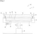
- a wafer heating and holding device is denoted by a reference symbol 10.
- the wafer heating and holding device 10 is a wafer heating and holding device of a wafer rotating and holding device 11, and comprises: a rotary shaft 18; a rotary table 12 placed on an end of the rotary shaft 18 and configured to hold a wafer W on an upper surface of the rotary table 12; a drive motor 20 configured to supply motive power to the rotary shaft 18; and heating means 14 provided above the rotary table 12 and below the wafer W without being in contact with the wafer W to heat the wafer W.
- the heating means 14 is disposed between the rotary table 12 and the wafer W to heat the wafer W directly while avoiding contact between the heating means 14 and the wafer W. It is therefore possible to cause the temperature of the wafer W alone to rise, to thereby heat the wafer W efficiently under reduced external influence. As a result, it is possible to perform spin processing under a state in which an in-plane temperature distribution is maintained.
- a reflective board is denoted by a reference symbol 16.
- the wafer heating and holding device comprises the reflective board 16 and disposes the heating means 14 on the reflective board 16 so that heat is not transmitted to the rotary table 12. It is preferred to provide a space between the reflective board 16 and the rotary table 12 with the use of a spacer 28.
- a resin sheet 26 is provided on the heating means 14 in order to prevent liquids from coming into contact with the heating means 14.
- a synthetic resin sheet for example, a fluororesin sheet, is a preferred resin sheet.
- the resin sheet used in FIG. 1 is a PFA sheet.
- the heating means 14 is not particularly limited and can be a known heater.
- a preferred heater is a carbon heater or a halogen heater, for example.
- FIG. 3 is a block diagram of a heating mechanism in the wafer heating and holding mechanism for the rotary table according to the present invention.
- the temperature of the wafer W is detected with a temperature sensor 34 constantly while current from a power source 30 is applied.
- the wafer W is rotated, and the heating means 14, which is a heater or the like, is powered on with the use of a SW circuit 36 to start heating by the heating means 14.
- a signal received from the temperature sensor 34 is used to control the powering on/off of the heater 14 with the SW circuit 36.
- a temperature fuse 38 and a bimetal 40 may be used to control the powering on/off of the heating means 14.
- outer peripheral pins which support the outer periphery of the wafer, are each denoted by a reference symbol 22 and support pins, which support a lower surface of the wafer W, are each denoted by a reference symbol 24. It is preferred to configure at least one of the outer peripheral pins 22 as a movable pin, which can be moved so as to open and close when the wafer is set.
- the rotary shaft 18 is made of stainless steel (SUS), and the rotary table 12 is made of industrial plastic or other types of synthetic resin.
- the number of revolutions of the rotary table 12 is not particularly limited, but 100 rpm to 1,000 rpm is preferred.
- a silicon wafer is preferred as the wafer W.
- electric power is supplied to the heating means 14.
- methods of supplying electric power there can be given, for example, one in which electric power is supplied from a battery embedded in the rotary table and motor driving is switched with a centrifugal force obtained by rotating the rotary table, one in which electric power is supplied from the rotary shaft by utilizing a slip ring to start rotation at the same time as electric power feeding, and one in which electric power is supplied to the rotary table with the use of electromagnetic induction to start rotation at the same time as electric power feeding.
- electric power is supplied to the heating means 14 from a power source provided in a lower part of the rotary table 12, via electric wires 32.
- An electric power supply mechanism 70 is illustrated in FIG. 4 as a mode of carrying out electric power supply means that uses the method of using the electromagnetic induction.
- the electric power supply mechanism 70 in FIG. 4 comprises: the rotary shaft 18; the rotary table 12 placed on an end of the rotary shaft 18 and configured to hold the wafer W on the upper surface of the rotary table 12; the drive motor 20 configured to supply motive power to the rotary shaft 18; a fixed-side primary coil 72 wound around the rotary shaft 18; an electric power supply source 74 connected to the fixed-side primary coil 72; and a rotary table-side secondary coil 76, which is provided so as to correspond to the fixed-side primary coil 72 and be separated from the fixed-side primary coil 72 by a predetermined distance, and is mounted to the rotary table 12.
- a heating means 14 is connected to the rotary table-side secondary coil 76 via electric wires 80 so that electric power is supplied to the heating means 14 by electromagnetic induction via the secondary coil 76.
- the wafer rotating and holding device comprises a spin processing mechanism.
- the spin processing mechanism is, for example, an etching processing mechanism in a spin etching device, a drying mechanism in a spin drying device, or a coating mechanism in a spin coating device.
- spin processing mechanisms there can be given, as processing to be performed on a wafer surface in manufacturing processes for a device, in addition to the etching processing mechanism for removing a damaged layer after back-grinding, a mechanism for applying developer to the wafer, a mechanism for performing developing processing on the wafer, which has a surface that has circuit patterns exposed thereon and is applied with developer, and which is printed with a semiconductor circuit, and a mechanism for cleaning the wafer surface, and the like.
- Chemical solutions to be used in the processing are not particularly limited, and acid-based/alkaline-based etching cleaning liquids and rinse water can be suitably used.
- a wafer substrate is heated directly and constantly during spin processing by heating means disposed between the rotary table and the wafer substrate, with the result that it is possible to perform stable spin processing under a state in which the in-plane temperature distribution is maintained.
- Etching can be performed under reduced external influence because of the direct heating of the wafer. For instance, when SiO 2 is to be removed with an HF etchant and the etchant is supplied at room temperature without being heated, the HF etchant is heated on the wafer by heating the wafer directly, and the etching rate thereof is raised as a result. This lessens the deterioration of HF etchant and prolongs the life thereof. According to the present invention, the risk of using HF, which is highly volatile and thus dangerous at a raised temperature, is reduced as well.
- a wafer heating method for a rotary table according to the present invention is a method of heating a wafer with the use of the wafer heating and holding device.
- the wafer rotating and holding device is a device comprising the wafer heating and holding device.
Landscapes
- Physics & Mathematics (AREA)
- Electromagnetism (AREA)
- General Physics & Mathematics (AREA)
- Container, Conveyance, Adherence, Positioning, Of Wafer (AREA)
- Cleaning Or Drying Semiconductors (AREA)
- Exposure Of Semiconductors, Excluding Electron Or Ion Beam Exposure (AREA)
Claims (3)
- Eine Wafer-Heiz- und Haltevorrichtung (10), die Folgendes umfasst:eine rotierende Welle (18);einen Drehtisch (12, 32), der an einem Ende der Drehwelle (18) angeordnet und so konfiguriert ist, dass er einen Wafer (W) hält;einen Antriebsmotor (20), der so konfiguriert ist, dass er die Drehwelle (18) mit Antriebskraft versorgt;Heizmittel (14), das innerhalb des Drehtisches (12, 32) und unterhalb des Wafers (W) vorgesehen ist, wobei ein Kontakt mit dem Wafer (W) vermieden wird, um den Wafer (W) zu erwärmen, eine reflektierende Platte (16), die zwischen dem Drehtisch (12, 32) und dem Heizmittel (14) vorgesehen ist, eine Harzplatte (26), wobei die Harzplatte (26) auf dem Heizmittel (14) vorgesehen ist,einen kontaktlosen elektrischen Stromversorgungsmechanismus (70) für einen Drehtisch (12, 32), der Folgendes umfasst:eine feststehende Primärspule (72), die um die Drehwelle (18) gewickelt ist;eine elektrische Stromversorgungsquelle (74), die mit der feststehenden Primärspule (72) verbunden ist;eine rotationstischseitige Sekundärspule (76), die so vorgesehen ist, dass sie mit der feststehenden Primärspule (72) korrespondiert und von der feststehenden Primärspule (72) durch einen vorbestimmten Abstand getrennt ist, und die an dem Rotationstisch (12, 32) angebracht ist;wobei die Wafer-Heiz- und Haltevorrichtung so ausgelegt ist, dass sie den kontaktlosen elektrischen Stromversorgungsmechanismus verwendet, wobei das Heizmittel (14) mit der drehschalterseitigen Sekundärspule (76) verbunden ist, und
wobei die Heizeinrichtung (14) über die drehschalterseitige Sekundärspule (76) durch elektromagnetische Induktion mit elektrischer Energie versorgt wird; - Wafererwärmungsverfahren für einen Drehtisch (12, 32), umfassend das Erwärmen des Wafers (W) unter Verwendung der Wafererwärmungs- und -haltevorrichtung (10) nach Anspruch 1.
- Wafer-Dreh- und -Haltevorrichtung (11), die die Wafer-Heiz- und -Haltevorrichtung (10) nach Anspruch 1 umfasst und ferner einen Mechanismus zum Durchführen von Spin-Ätzen, Spin-Trocknen, Spin-Beschichten, einen Mechanismus zum Durchführen von Herstellungsprozessen für eine Vorrichtung auf einer Wafer-Oberfläche, einen Mechanismus zum Entfernen einer beschädigten Schicht nach dem Rückschleifen, einen Mechanismus zum Auftragen von Entwicklungsmittel auf den Wafer, einen Mechanismus zum Durchführen eines Entwicklungsprozesses auf dem Wafer, der eine Oberfläche aufweist, auf der Schaltungsmuster freigelegt sind und die mit Entwicklungsmittel beaufschlagt ist und die mit einer Halbleiterschaltung bedruckt ist, und einen Mechanismus zum Reinigen der Wafer-Oberfläche umfasst.
Applications Claiming Priority (2)
| Application Number | Priority Date | Filing Date | Title |
|---|---|---|---|
| JP2016105591 | 2016-05-26 | ||
| PCT/JP2017/018696 WO2017204083A1 (ja) | 2016-05-26 | 2017-05-18 | 回転テーブル用ウェーハ加熱保持機構及び方法並びにウェーハ回転保持装置 |
Publications (3)
| Publication Number | Publication Date |
|---|---|
| EP3442016A1 EP3442016A1 (de) | 2019-02-13 |
| EP3442016A4 EP3442016A4 (de) | 2019-11-13 |
| EP3442016B1 true EP3442016B1 (de) | 2023-06-07 |
Family
ID=60411260
Family Applications (1)
| Application Number | Title | Priority Date | Filing Date |
|---|---|---|---|
| EP17802675.3A Active EP3442016B1 (de) | 2016-05-26 | 2017-05-18 | Wafererwärmungs- und -haltevorrichtung und -verfahren für drehtisch sowie waferdreh- und -haltevorrichtung |
Country Status (5)
| Country | Link |
|---|---|
| US (1) | US11056362B2 (de) |
| EP (1) | EP3442016B1 (de) |
| JP (1) | JP6837481B2 (de) |
| CN (1) | CN109155273B (de) |
| WO (1) | WO2017204083A1 (de) |
Families Citing this family (11)
| Publication number | Priority date | Publication date | Assignee | Title |
|---|---|---|---|---|
| JP6689719B2 (ja) * | 2016-09-23 | 2020-04-28 | 株式会社Screenホールディングス | 基板処理装置 |
| KR102111099B1 (ko) * | 2018-11-09 | 2020-05-15 | (주)에이앤아이 | 집전 픽업을 포함하는 무선 로터리 검사장치 |
| JP7241646B2 (ja) * | 2019-08-30 | 2023-03-17 | 京セラ株式会社 | ヒータ及びヒータシステム |
| JP7350613B2 (ja) | 2019-10-17 | 2023-09-26 | 東京エレクトロン株式会社 | 基板処理装置 |
| KR102898051B1 (ko) * | 2020-03-13 | 2025-12-10 | 삼성전자주식회사 | 펠리클 전사 장치 및 펠리클 전사 방법 |
| CN112133649A (zh) * | 2020-09-21 | 2020-12-25 | 南通大学 | 一种大尺寸晶片均匀高温腐蚀装置及其腐蚀方法 |
| KR102548766B1 (ko) * | 2020-11-02 | 2023-06-30 | 세메스 주식회사 | 기판 처리 장치 및 발열 부재 제어 방법 |
| US12025320B2 (en) * | 2020-12-15 | 2024-07-02 | Arash Kani | Moving heating element |
| KR102683732B1 (ko) * | 2021-04-01 | 2024-07-12 | 세메스 주식회사 | 지지 유닛 및 기판 처리 장치 |
| JP2025119244A (ja) * | 2024-02-01 | 2025-08-14 | 株式会社Screenホールディングス | 基板保持装置および基板処理装置 |
| JP2025122789A (ja) * | 2024-02-09 | 2025-08-22 | 株式会社Screenホールディングス | 基板保持装置および基板処理装置 |
Citations (2)
| Publication number | Priority date | Publication date | Assignee | Title |
|---|---|---|---|---|
| JPH06232047A (ja) * | 1993-01-29 | 1994-08-19 | Mitsubishi Heavy Ind Ltd | ウェハ回転装置 |
| JP2008103521A (ja) * | 2006-10-19 | 2008-05-01 | Dainippon Screen Mfg Co Ltd | 基板回転保持装置および基板処理装置 |
Family Cites Families (15)
| Publication number | Priority date | Publication date | Assignee | Title |
|---|---|---|---|---|
| JPH09181155A (ja) * | 1995-09-29 | 1997-07-11 | Applied Materials Inc | 堆積装置のサセプタ |
| JP4111479B2 (ja) * | 1999-09-09 | 2008-07-02 | 三益半導体工業株式会社 | ウェーハ回転保持装置 |
| JP4257816B2 (ja) | 2000-03-16 | 2009-04-22 | 三益半導体工業株式会社 | 廃液回収機構付ウェーハ表面処理装置 |
| JP3592233B2 (ja) * | 2000-12-14 | 2004-11-24 | 大日本スクリーン製造株式会社 | 基板表面処理装置および基板表面処理方法 |
| JP4067858B2 (ja) * | 2002-04-16 | 2008-03-26 | 東京エレクトロン株式会社 | Ald成膜装置およびald成膜方法 |
| JP2004072000A (ja) * | 2002-08-09 | 2004-03-04 | Matsushita Electric Ind Co Ltd | 加熱装置 |
| JP4364242B2 (ja) | 2004-03-22 | 2009-11-11 | 三益半導体工業株式会社 | スピンエッチングにおける工程管理方法及びスピンエッチング装置 |
| US20090032498A1 (en) * | 2005-03-30 | 2009-02-05 | Mimasu Semiconductor Industry Co., Ltd. | Spin Processing Method And Apparatus |
| JP2007335709A (ja) * | 2006-06-16 | 2007-12-27 | Dainippon Screen Mfg Co Ltd | 基板処理装置 |
| JP4933409B2 (ja) * | 2007-11-29 | 2012-05-16 | 株式会社ニューフレアテクノロジー | 半導体製造装置および半導体製造方法 |
| JP2010087197A (ja) * | 2008-09-30 | 2010-04-15 | M Setek Co Ltd | レジスト塗布装置 |
| JP6351948B2 (ja) * | 2012-10-12 | 2018-07-04 | ラム・リサーチ・アーゲーLam Research Ag | 円板状物品の液体処理装置およびかかる装置で用いる加熱システム |
| JP6036189B2 (ja) | 2012-11-07 | 2016-11-30 | ソニー株式会社 | アンテナモジュール、情報通信装置及び情報通信システム |
| KR102124417B1 (ko) * | 2012-11-27 | 2020-06-24 | 에이씨엠 리서치 (상하이) 인코포레이티드 | 기판 지지 장치 |
| DE102016103270B3 (de) | 2016-02-24 | 2017-05-11 | Ev Group E. Thallner Gmbh | Vorrichtung und Verfahren zur Halterung, Rotation sowie Heizung und/oder Kühlung eines Substrats |
-
2017
- 2017-05-18 EP EP17802675.3A patent/EP3442016B1/de active Active
- 2017-05-18 JP JP2018519230A patent/JP6837481B2/ja active Active
- 2017-05-18 WO PCT/JP2017/018696 patent/WO2017204083A1/ja not_active Ceased
- 2017-05-18 US US16/304,385 patent/US11056362B2/en active Active
- 2017-05-18 CN CN201780031237.8A patent/CN109155273B/zh active Active
Patent Citations (2)
| Publication number | Priority date | Publication date | Assignee | Title |
|---|---|---|---|---|
| JPH06232047A (ja) * | 1993-01-29 | 1994-08-19 | Mitsubishi Heavy Ind Ltd | ウェハ回転装置 |
| JP2008103521A (ja) * | 2006-10-19 | 2008-05-01 | Dainippon Screen Mfg Co Ltd | 基板回転保持装置および基板処理装置 |
Also Published As
| Publication number | Publication date |
|---|---|
| US20190295866A1 (en) | 2019-09-26 |
| CN109155273A (zh) | 2019-01-04 |
| WO2017204083A1 (ja) | 2017-11-30 |
| US11056362B2 (en) | 2021-07-06 |
| CN109155273B (zh) | 2024-01-02 |
| JPWO2017204083A1 (ja) | 2019-03-14 |
| EP3442016A1 (de) | 2019-02-13 |
| JP6837481B2 (ja) | 2021-03-03 |
| EP3442016A4 (de) | 2019-11-13 |
Similar Documents
| Publication | Publication Date | Title |
|---|---|---|
| US11056362B2 (en) | Wafer heating and holding mechanism and method for rotary table, and wafer rotating and holding device | |
| EP3442015B1 (de) | Waferhaltemechanismus und verfahren für drehtisch und drehwaferhaltevorrichtung | |
| KR102088539B1 (ko) | 기판 처리 방법 및 기판 처리 장치 | |
| US6749484B2 (en) | Chemical mechanical polishing (CMP) apparatus with temperature control | |
| KR20140135127A (ko) | 웨이퍼 형상 물체의 액체 처리를 위한 장치 및 이러한 장치에서 사용되는 가열 시스템 | |
| JP5712101B2 (ja) | 基板処理方法及び基板処理装置 | |
| US11862489B2 (en) | Substrate processing apparatus with electronic heater powered by power feeding coil | |
| JP2017112220A (ja) | 基板処理装置および基板処理方法 | |
| EP3432351B1 (de) | Mechanismus und verfahren zur kontaktlosen stromversorgung für drehtisch und waferdreh- und -haltevorrichtung | |
| JP6642868B2 (ja) | 基板処理方法および基板処理装置 | |
| KR20080082846A (ko) | 기판 박판화 방법, 기판 박판화 장치 및 이를 포함하는기판 박판화 시스템 | |
| JP5290358B2 (ja) | フィルム除去装置 | |
| CN107275258A (zh) | 基板处理装置 | |
| JP2020170801A (ja) | 基板処理方法および基板処理装置 | |
| JP7288770B2 (ja) | 基板処理方法および基板処理装置 | |
| JP6715078B2 (ja) | 回転テーブル用ウェーハ保持機構及び方法並びにウェーハ回転保持装置 | |
| KR20110080343A (ko) | 고온의 약액을 공급하는 장치 | |
| KR100846119B1 (ko) | 플라즈마 공급유닛 및 이를 구비하는 기판 처리 장치,그리고 상기 장치의 기판 처리 방법 | |
| CN111489955A (zh) | 基板处理方法以及基板处理装置 | |
| JPH10107134A (ja) | 静電吸着装置 | |
| KR20090018996A (ko) | 기판 박판화 방법, 기판 박판화 장치 및 이를 포함하는 기판 박판화 시스템 | |
| KR100909473B1 (ko) | 기판 처리 장치 | |
| KR20100131798A (ko) | 기판 처리 장치 | |
| JP2026021987A (ja) | スピンエッチング装置及びスピンエッチング方法 | |
| KR200151978Y1 (ko) | 반도체 소자 제조를 위한 감광막 제거용 베쓰의 히팅 시스템 |
Legal Events
| Date | Code | Title | Description |
|---|---|---|---|
| STAA | Information on the status of an ep patent application or granted ep patent |
Free format text: STATUS: THE INTERNATIONAL PUBLICATION HAS BEEN MADE |
|
| PUAI | Public reference made under article 153(3) epc to a published international application that has entered the european phase |
Free format text: ORIGINAL CODE: 0009012 |
|
| STAA | Information on the status of an ep patent application or granted ep patent |
Free format text: STATUS: REQUEST FOR EXAMINATION WAS MADE |
|
| 17P | Request for examination filed |
Effective date: 20181105 |
|
| AK | Designated contracting states |
Kind code of ref document: A1 Designated state(s): AL AT BE BG CH CY CZ DE DK EE ES FI FR GB GR HR HU IE IS IT LI LT LU LV MC MK MT NL NO PL PT RO RS SE SI SK SM TR |
|
| AX | Request for extension of the european patent |
Extension state: BA ME |
|
| DAV | Request for validation of the european patent (deleted) | ||
| DAX | Request for extension of the european patent (deleted) | ||
| A4 | Supplementary search report drawn up and despatched |
Effective date: 20191014 |
|
| RIC1 | Information provided on ipc code assigned before grant |
Ipc: H01L 21/67 20060101ALI20191008BHEP Ipc: H01L 21/027 20060101ALI20191008BHEP Ipc: H01L 21/304 20060101ALI20191008BHEP Ipc: H01L 21/683 20060101AFI20191008BHEP |
|
| STAA | Information on the status of an ep patent application or granted ep patent |
Free format text: STATUS: EXAMINATION IS IN PROGRESS |
|
| 17Q | First examination report despatched |
Effective date: 20210916 |
|
| GRAP | Despatch of communication of intention to grant a patent |
Free format text: ORIGINAL CODE: EPIDOSNIGR1 |
|
| STAA | Information on the status of an ep patent application or granted ep patent |
Free format text: STATUS: GRANT OF PATENT IS INTENDED |
|
| INTG | Intention to grant announced |
Effective date: 20221222 |
|
| GRAS | Grant fee paid |
Free format text: ORIGINAL CODE: EPIDOSNIGR3 |
|
| GRAA | (expected) grant |
Free format text: ORIGINAL CODE: 0009210 |
|
| STAA | Information on the status of an ep patent application or granted ep patent |
Free format text: STATUS: THE PATENT HAS BEEN GRANTED |
|
| AK | Designated contracting states |
Kind code of ref document: B1 Designated state(s): AL AT BE BG CH CY CZ DE DK EE ES FI FR GB GR HR HU IE IS IT LI LT LU LV MC MK MT NL NO PL PT RO RS SE SI SK SM TR |
|
| REG | Reference to a national code |
Ref country code: GB Ref legal event code: FG4D |
|
| REG | Reference to a national code |
Ref country code: CH Ref legal event code: EP Ref country code: AT Ref legal event code: REF Ref document number: 1577539 Country of ref document: AT Kind code of ref document: T Effective date: 20230615 |
|
| REG | Reference to a national code |
Ref country code: DE Ref legal event code: R096 Ref document number: 602017069772 Country of ref document: DE |
|
| REG | Reference to a national code |
Ref country code: LT Ref legal event code: MG9D |
|
| REG | Reference to a national code |
Ref country code: NL Ref legal event code: MP Effective date: 20230607 |
|
| PG25 | Lapsed in a contracting state [announced via postgrant information from national office to epo] |
Ref country code: SE Free format text: LAPSE BECAUSE OF FAILURE TO SUBMIT A TRANSLATION OF THE DESCRIPTION OR TO PAY THE FEE WITHIN THE PRESCRIBED TIME-LIMIT Effective date: 20230607 Ref country code: NO Free format text: LAPSE BECAUSE OF FAILURE TO SUBMIT A TRANSLATION OF THE DESCRIPTION OR TO PAY THE FEE WITHIN THE PRESCRIBED TIME-LIMIT Effective date: 20230907 Ref country code: ES Free format text: LAPSE BECAUSE OF FAILURE TO SUBMIT A TRANSLATION OF THE DESCRIPTION OR TO PAY THE FEE WITHIN THE PRESCRIBED TIME-LIMIT Effective date: 20230607 |
|
| PG25 | Lapsed in a contracting state [announced via postgrant information from national office to epo] |
Ref country code: RS Free format text: LAPSE BECAUSE OF FAILURE TO SUBMIT A TRANSLATION OF THE DESCRIPTION OR TO PAY THE FEE WITHIN THE PRESCRIBED TIME-LIMIT Effective date: 20230607 Ref country code: NL Free format text: LAPSE BECAUSE OF FAILURE TO SUBMIT A TRANSLATION OF THE DESCRIPTION OR TO PAY THE FEE WITHIN THE PRESCRIBED TIME-LIMIT Effective date: 20230607 Ref country code: LV Free format text: LAPSE BECAUSE OF FAILURE TO SUBMIT A TRANSLATION OF THE DESCRIPTION OR TO PAY THE FEE WITHIN THE PRESCRIBED TIME-LIMIT Effective date: 20230607 Ref country code: LT Free format text: LAPSE BECAUSE OF FAILURE TO SUBMIT A TRANSLATION OF THE DESCRIPTION OR TO PAY THE FEE WITHIN THE PRESCRIBED TIME-LIMIT Effective date: 20230607 Ref country code: HR Free format text: LAPSE BECAUSE OF FAILURE TO SUBMIT A TRANSLATION OF THE DESCRIPTION OR TO PAY THE FEE WITHIN THE PRESCRIBED TIME-LIMIT Effective date: 20230607 Ref country code: GR Free format text: LAPSE BECAUSE OF FAILURE TO SUBMIT A TRANSLATION OF THE DESCRIPTION OR TO PAY THE FEE WITHIN THE PRESCRIBED TIME-LIMIT Effective date: 20230908 |
|
| PG25 | Lapsed in a contracting state [announced via postgrant information from national office to epo] |
Ref country code: FI Free format text: LAPSE BECAUSE OF FAILURE TO SUBMIT A TRANSLATION OF THE DESCRIPTION OR TO PAY THE FEE WITHIN THE PRESCRIBED TIME-LIMIT Effective date: 20230607 |
|
| PG25 | Lapsed in a contracting state [announced via postgrant information from national office to epo] |
Ref country code: SK Free format text: LAPSE BECAUSE OF FAILURE TO SUBMIT A TRANSLATION OF THE DESCRIPTION OR TO PAY THE FEE WITHIN THE PRESCRIBED TIME-LIMIT Effective date: 20230607 |
|
| PG25 | Lapsed in a contracting state [announced via postgrant information from national office to epo] |
Ref country code: IS Free format text: LAPSE BECAUSE OF FAILURE TO SUBMIT A TRANSLATION OF THE DESCRIPTION OR TO PAY THE FEE WITHIN THE PRESCRIBED TIME-LIMIT Effective date: 20231007 |
|
| PG25 | Lapsed in a contracting state [announced via postgrant information from national office to epo] |
Ref country code: SM Free format text: LAPSE BECAUSE OF FAILURE TO SUBMIT A TRANSLATION OF THE DESCRIPTION OR TO PAY THE FEE WITHIN THE PRESCRIBED TIME-LIMIT Effective date: 20230607 Ref country code: SK Free format text: LAPSE BECAUSE OF FAILURE TO SUBMIT A TRANSLATION OF THE DESCRIPTION OR TO PAY THE FEE WITHIN THE PRESCRIBED TIME-LIMIT Effective date: 20230607 Ref country code: RO Free format text: LAPSE BECAUSE OF FAILURE TO SUBMIT A TRANSLATION OF THE DESCRIPTION OR TO PAY THE FEE WITHIN THE PRESCRIBED TIME-LIMIT Effective date: 20230607 Ref country code: PT Free format text: LAPSE BECAUSE OF FAILURE TO SUBMIT A TRANSLATION OF THE DESCRIPTION OR TO PAY THE FEE WITHIN THE PRESCRIBED TIME-LIMIT Effective date: 20231009 Ref country code: IS Free format text: LAPSE BECAUSE OF FAILURE TO SUBMIT A TRANSLATION OF THE DESCRIPTION OR TO PAY THE FEE WITHIN THE PRESCRIBED TIME-LIMIT Effective date: 20231007 Ref country code: EE Free format text: LAPSE BECAUSE OF FAILURE TO SUBMIT A TRANSLATION OF THE DESCRIPTION OR TO PAY THE FEE WITHIN THE PRESCRIBED TIME-LIMIT Effective date: 20230607 Ref country code: CZ Free format text: LAPSE BECAUSE OF FAILURE TO SUBMIT A TRANSLATION OF THE DESCRIPTION OR TO PAY THE FEE WITHIN THE PRESCRIBED TIME-LIMIT Effective date: 20230607 |
|
| PG25 | Lapsed in a contracting state [announced via postgrant information from national office to epo] |
Ref country code: PL Free format text: LAPSE BECAUSE OF FAILURE TO SUBMIT A TRANSLATION OF THE DESCRIPTION OR TO PAY THE FEE WITHIN THE PRESCRIBED TIME-LIMIT Effective date: 20230607 |
|
| REG | Reference to a national code |
Ref country code: DE Ref legal event code: R097 Ref document number: 602017069772 Country of ref document: DE |
|
| PLBE | No opposition filed within time limit |
Free format text: ORIGINAL CODE: 0009261 |
|
| STAA | Information on the status of an ep patent application or granted ep patent |
Free format text: STATUS: NO OPPOSITION FILED WITHIN TIME LIMIT |
|
| PG25 | Lapsed in a contracting state [announced via postgrant information from national office to epo] |
Ref country code: DK Free format text: LAPSE BECAUSE OF FAILURE TO SUBMIT A TRANSLATION OF THE DESCRIPTION OR TO PAY THE FEE WITHIN THE PRESCRIBED TIME-LIMIT Effective date: 20230607 |
|
| PG25 | Lapsed in a contracting state [announced via postgrant information from national office to epo] |
Ref country code: SI Free format text: LAPSE BECAUSE OF FAILURE TO SUBMIT A TRANSLATION OF THE DESCRIPTION OR TO PAY THE FEE WITHIN THE PRESCRIBED TIME-LIMIT Effective date: 20230607 |
|
| 26N | No opposition filed |
Effective date: 20240308 |
|
| PG25 | Lapsed in a contracting state [announced via postgrant information from national office to epo] |
Ref country code: SI Free format text: LAPSE BECAUSE OF FAILURE TO SUBMIT A TRANSLATION OF THE DESCRIPTION OR TO PAY THE FEE WITHIN THE PRESCRIBED TIME-LIMIT Effective date: 20230607 Ref country code: IT Free format text: LAPSE BECAUSE OF FAILURE TO SUBMIT A TRANSLATION OF THE DESCRIPTION OR TO PAY THE FEE WITHIN THE PRESCRIBED TIME-LIMIT Effective date: 20230607 |
|
| PG25 | Lapsed in a contracting state [announced via postgrant information from national office to epo] |
Ref country code: BG Free format text: LAPSE BECAUSE OF FAILURE TO SUBMIT A TRANSLATION OF THE DESCRIPTION OR TO PAY THE FEE WITHIN THE PRESCRIBED TIME-LIMIT Effective date: 20230607 |
|
| PG25 | Lapsed in a contracting state [announced via postgrant information from national office to epo] |
Ref country code: BG Free format text: LAPSE BECAUSE OF FAILURE TO SUBMIT A TRANSLATION OF THE DESCRIPTION OR TO PAY THE FEE WITHIN THE PRESCRIBED TIME-LIMIT Effective date: 20230607 |
|
| PG25 | Lapsed in a contracting state [announced via postgrant information from national office to epo] |
Ref country code: MC Free format text: LAPSE BECAUSE OF FAILURE TO SUBMIT A TRANSLATION OF THE DESCRIPTION OR TO PAY THE FEE WITHIN THE PRESCRIBED TIME-LIMIT Effective date: 20230607 |
|
| PG25 | Lapsed in a contracting state [announced via postgrant information from national office to epo] |
Ref country code: LU Free format text: LAPSE BECAUSE OF NON-PAYMENT OF DUE FEES Effective date: 20240518 |
|
| PG25 | Lapsed in a contracting state [announced via postgrant information from national office to epo] |
Ref country code: MC Free format text: LAPSE BECAUSE OF FAILURE TO SUBMIT A TRANSLATION OF THE DESCRIPTION OR TO PAY THE FEE WITHIN THE PRESCRIBED TIME-LIMIT Effective date: 20230607 Ref country code: LU Free format text: LAPSE BECAUSE OF NON-PAYMENT OF DUE FEES Effective date: 20240518 |
|
| REG | Reference to a national code |
Ref country code: BE Ref legal event code: MM Effective date: 20240531 |
|
| PG25 | Lapsed in a contracting state [announced via postgrant information from national office to epo] |
Ref country code: IE Free format text: LAPSE BECAUSE OF NON-PAYMENT OF DUE FEES Effective date: 20240518 |
|
| PG25 | Lapsed in a contracting state [announced via postgrant information from national office to epo] |
Ref country code: BE Free format text: LAPSE BECAUSE OF NON-PAYMENT OF DUE FEES Effective date: 20240531 |
|
| PG25 | Lapsed in a contracting state [announced via postgrant information from national office to epo] |
Ref country code: FR Free format text: LAPSE BECAUSE OF NON-PAYMENT OF DUE FEES Effective date: 20240531 |
|
| PG25 | Lapsed in a contracting state [announced via postgrant information from national office to epo] |
Ref country code: CY Free format text: LAPSE BECAUSE OF FAILURE TO SUBMIT A TRANSLATION OF THE DESCRIPTION OR TO PAY THE FEE WITHIN THE PRESCRIBED TIME-LIMIT; INVALID AB INITIO Effective date: 20170518 |
|
| PG25 | Lapsed in a contracting state [announced via postgrant information from national office to epo] |
Ref country code: HU Free format text: LAPSE BECAUSE OF FAILURE TO SUBMIT A TRANSLATION OF THE DESCRIPTION OR TO PAY THE FEE WITHIN THE PRESCRIBED TIME-LIMIT; INVALID AB INITIO Effective date: 20170518 |
|
| REG | Reference to a national code |
Ref country code: DE Ref legal event code: R079 Ref document number: 602017069772 Country of ref document: DE Free format text: PREVIOUS MAIN CLASS: H01L0021683000 Ipc: H10P0072700000 |
|
| PG25 | Lapsed in a contracting state [announced via postgrant information from national office to epo] |
Ref country code: TR Free format text: LAPSE BECAUSE OF FAILURE TO SUBMIT A TRANSLATION OF THE DESCRIPTION OR TO PAY THE FEE WITHIN THE PRESCRIBED TIME-LIMIT Effective date: 20230607 |
|
| REG | Reference to a national code |
Ref country code: CH Ref legal event code: U11 Free format text: ST27 STATUS EVENT CODE: U-0-0-U10-U11 (AS PROVIDED BY THE NATIONAL OFFICE) Effective date: 20260601 |
|
| PGFP | Annual fee paid to national office [announced via postgrant information from national office to epo] |
Ref country code: GB Payment date: 20260522 Year of fee payment: 10 |
|
| PGFP | Annual fee paid to national office [announced via postgrant information from national office to epo] |
Ref country code: DE Payment date: 20260522 Year of fee payment: 10 |
|
| PGFP | Annual fee paid to national office [announced via postgrant information from national office to epo] |
Ref country code: AT Payment date: 20260521 Year of fee payment: 10 |
|
| PGFP | Annual fee paid to national office [announced via postgrant information from national office to epo] |
Ref country code: CH Payment date: 20260601 Year of fee payment: 10 |