EP3442031A2 - Dispositif à semi-conducteur et son procédé de fabrication - Google Patents
Dispositif à semi-conducteur et son procédé de fabrication Download PDFInfo
- Publication number
- EP3442031A2 EP3442031A2 EP18159566.1A EP18159566A EP3442031A2 EP 3442031 A2 EP3442031 A2 EP 3442031A2 EP 18159566 A EP18159566 A EP 18159566A EP 3442031 A2 EP3442031 A2 EP 3442031A2
- Authority
- EP
- European Patent Office
- Prior art keywords
- layer
- semiconductor
- region
- insulating layer
- capacitive element
- Prior art date
- Legal status (The legal status is an assumption and is not a legal conclusion. Google has not performed a legal analysis and makes no representation as to the accuracy of the status listed.)
- Withdrawn
Links
Images


Classifications
-
- H—ELECTRICITY
- H10—SEMICONDUCTOR DEVICES; ELECTRIC SOLID-STATE DEVICES NOT OTHERWISE PROVIDED FOR
- H10W—GENERIC PACKAGES, INTERCONNECTIONS, CONNECTORS OR OTHER CONSTRUCTIONAL DETAILS OF DEVICES COVERED BY CLASS H10
- H10W20/00—Interconnections in chips, wafers or substrates
- H10W20/40—Interconnections external to wafers or substrates, e.g. back-end-of-line [BEOL] metallisations or vias connecting to gate electrodes
- H10W20/495—Capacitive arrangements or effects of, or between wiring layers
- H10W20/496—Capacitor integral with wiring layers
-
- H—ELECTRICITY
- H10—SEMICONDUCTOR DEVICES; ELECTRIC SOLID-STATE DEVICES NOT OTHERWISE PROVIDED FOR
- H10B—ELECTRONIC MEMORY DEVICES
- H10B41/00—Electrically erasable-and-programmable ROM [EEPROM] devices comprising floating gates
- H10B41/30—Electrically erasable-and-programmable ROM [EEPROM] devices comprising floating gates characterised by the memory core region
-
- H—ELECTRICITY
- H10—SEMICONDUCTOR DEVICES; ELECTRIC SOLID-STATE DEVICES NOT OTHERWISE PROVIDED FOR
- H10B—ELECTRONIC MEMORY DEVICES
- H10B41/00—Electrically erasable-and-programmable ROM [EEPROM] devices comprising floating gates
-
- H—ELECTRICITY
- H10—SEMICONDUCTOR DEVICES; ELECTRIC SOLID-STATE DEVICES NOT OTHERWISE PROVIDED FOR
- H10B—ELECTRONIC MEMORY DEVICES
- H10B41/00—Electrically erasable-and-programmable ROM [EEPROM] devices comprising floating gates
- H10B41/40—Electrically erasable-and-programmable ROM [EEPROM] devices comprising floating gates characterised by the peripheral circuit region
-
- H—ELECTRICITY
- H10—SEMICONDUCTOR DEVICES; ELECTRIC SOLID-STATE DEVICES NOT OTHERWISE PROVIDED FOR
- H10B—ELECTRONIC MEMORY DEVICES
- H10B43/00—EEPROM devices comprising charge-trapping gate insulators
-
- H—ELECTRICITY
- H10—SEMICONDUCTOR DEVICES; ELECTRIC SOLID-STATE DEVICES NOT OTHERWISE PROVIDED FOR
- H10B—ELECTRONIC MEMORY DEVICES
- H10B43/00—EEPROM devices comprising charge-trapping gate insulators
- H10B43/40—EEPROM devices comprising charge-trapping gate insulators characterised by the peripheral circuit region
-
- H—ELECTRICITY
- H10—SEMICONDUCTOR DEVICES; ELECTRIC SOLID-STATE DEVICES NOT OTHERWISE PROVIDED FOR
- H10D—INORGANIC ELECTRIC SEMICONDUCTOR DEVICES
- H10D1/00—Resistors, capacitors or inductors
- H10D1/60—Capacitors
- H10D1/62—Capacitors having potential barriers
- H10D1/66—Conductor-insulator-semiconductor capacitors, e.g. MOS capacitors
-
- H—ELECTRICITY
- H10—SEMICONDUCTOR DEVICES; ELECTRIC SOLID-STATE DEVICES NOT OTHERWISE PROVIDED FOR
- H10D—INORGANIC ELECTRIC SEMICONDUCTOR DEVICES
- H10D1/00—Resistors, capacitors or inductors
- H10D1/60—Capacitors
- H10D1/68—Capacitors having no potential barriers
-
- H—ELECTRICITY
- H10—SEMICONDUCTOR DEVICES; ELECTRIC SOLID-STATE DEVICES NOT OTHERWISE PROVIDED FOR
- H10D—INORGANIC ELECTRIC SEMICONDUCTOR DEVICES
- H10D1/00—Resistors, capacitors or inductors
- H10D1/60—Capacitors
- H10D1/68—Capacitors having no potential barriers
- H10D1/692—Electrodes
-
- H—ELECTRICITY
- H10—SEMICONDUCTOR DEVICES; ELECTRIC SOLID-STATE DEVICES NOT OTHERWISE PROVIDED FOR
- H10D—INORGANIC ELECTRIC SEMICONDUCTOR DEVICES
- H10D84/00—Integrated devices formed in or on semiconductor substrates that comprise only semiconducting layers, e.g. on Si wafers or on GaAs-on-Si wafers
- H10D84/01—Manufacture or treatment
- H10D84/0123—Integrating together multiple components covered by H10D12/00 or H10D30/00, e.g. integrating multiple IGBTs
- H10D84/0126—Integrating together multiple components covered by H10D12/00 or H10D30/00, e.g. integrating multiple IGBTs the components including insulated gates, e.g. IGFETs
- H10D84/0144—Manufacturing their gate insulating layers
-
- H—ELECTRICITY
- H10—SEMICONDUCTOR DEVICES; ELECTRIC SOLID-STATE DEVICES NOT OTHERWISE PROVIDED FOR
- H10D—INORGANIC ELECTRIC SEMICONDUCTOR DEVICES
- H10D87/00—Integrated devices comprising both bulk components and either SOI or SOS components on the same substrate
-
- H—ELECTRICITY
- H10—SEMICONDUCTOR DEVICES; ELECTRIC SOLID-STATE DEVICES NOT OTHERWISE PROVIDED FOR
- H10W—GENERIC PACKAGES, INTERCONNECTIONS, CONNECTORS OR OTHER CONSTRUCTIONAL DETAILS OF DEVICES COVERED BY CLASS H10
- H10W10/00—Isolation regions in semiconductor bodies between components of integrated devices
- H10W10/01—Manufacture or treatment
- H10W10/011—Manufacture or treatment of isolation regions comprising dielectric materials
-
- H—ELECTRICITY
- H10—SEMICONDUCTOR DEVICES; ELECTRIC SOLID-STATE DEVICES NOT OTHERWISE PROVIDED FOR
- H10W—GENERIC PACKAGES, INTERCONNECTIONS, CONNECTORS OR OTHER CONSTRUCTIONAL DETAILS OF DEVICES COVERED BY CLASS H10
- H10W10/00—Isolation regions in semiconductor bodies between components of integrated devices
- H10W10/10—Isolation regions comprising dielectric materials
-
- H—ELECTRICITY
- H10—SEMICONDUCTOR DEVICES; ELECTRIC SOLID-STATE DEVICES NOT OTHERWISE PROVIDED FOR
- H10W—GENERIC PACKAGES, INTERCONNECTIONS, CONNECTORS OR OTHER CONSTRUCTIONAL DETAILS OF DEVICES COVERED BY CLASS H10
- H10W20/00—Interconnections in chips, wafers or substrates
- H10W20/01—Manufacture or treatment
- H10W20/031—Manufacture or treatment of conductive parts of the interconnections
- H10W20/056—Manufacture or treatment of conductive parts of the interconnections by filling conductive material into holes, grooves or trenches
-
- H—ELECTRICITY
- H10—SEMICONDUCTOR DEVICES; ELECTRIC SOLID-STATE DEVICES NOT OTHERWISE PROVIDED FOR
- H10W—GENERIC PACKAGES, INTERCONNECTIONS, CONNECTORS OR OTHER CONSTRUCTIONAL DETAILS OF DEVICES COVERED BY CLASS H10
- H10W20/00—Interconnections in chips, wafers or substrates
- H10W20/40—Interconnections external to wafers or substrates, e.g. back-end-of-line [BEOL] metallisations or vias connecting to gate electrodes
- H10W20/45—Interconnections external to wafers or substrates, e.g. back-end-of-line [BEOL] metallisations or vias connecting to gate electrodes characterised by their insulating parts
- H10W20/47—Interconnections external to wafers or substrates, e.g. back-end-of-line [BEOL] metallisations or vias connecting to gate electrodes characterised by their insulating parts comprising two or more dielectric layers having different properties, e.g. different dielectric constants
-
- H—ELECTRICITY
- H10—SEMICONDUCTOR DEVICES; ELECTRIC SOLID-STATE DEVICES NOT OTHERWISE PROVIDED FOR
- H10D—INORGANIC ELECTRIC SEMICONDUCTOR DEVICES
- H10D84/00—Integrated devices formed in or on semiconductor substrates that comprise only semiconducting layers, e.g. on Si wafers or on GaAs-on-Si wafers
- H10D84/201—Integrated devices formed in or on semiconductor substrates that comprise only semiconducting layers, e.g. on Si wafers or on GaAs-on-Si wafers characterised by the integration of only components covered by H10D1/00 or H10D8/00, e.g. RLC circuits
- H10D84/204—Integrated devices formed in or on semiconductor substrates that comprise only semiconducting layers, e.g. on Si wafers or on GaAs-on-Si wafers characterised by the integration of only components covered by H10D1/00 or H10D8/00, e.g. RLC circuits of combinations of diodes or capacitors or resistors
- H10D84/212—Integrated devices formed in or on semiconductor substrates that comprise only semiconducting layers, e.g. on Si wafers or on GaAs-on-Si wafers characterised by the integration of only components covered by H10D1/00 or H10D8/00, e.g. RLC circuits of combinations of diodes or capacitors or resistors of only capacitors
-
- H—ELECTRICITY
- H10—SEMICONDUCTOR DEVICES; ELECTRIC SOLID-STATE DEVICES NOT OTHERWISE PROVIDED FOR
- H10D—INORGANIC ELECTRIC SEMICONDUCTOR DEVICES
- H10D84/00—Integrated devices formed in or on semiconductor substrates that comprise only semiconducting layers, e.g. on Si wafers or on GaAs-on-Si wafers
- H10D84/80—Integrated devices formed in or on semiconductor substrates that comprise only semiconducting layers, e.g. on Si wafers or on GaAs-on-Si wafers characterised by the integration of at least one component covered by groups H10D12/00 or H10D30/00, e.g. integration of IGFETs
- H10D84/811—Combinations of field-effect devices and one or more diodes, capacitors or resistors
- H10D84/813—Combinations of field-effect devices and capacitor only
Definitions
- the present invention relates to a semiconductor device and a manufacturing method thereof, and can be suitably used, for example, for a semiconductor device having a capacitive element and a manufacturing method thereof.
- Patent Document 1 discloses a semiconductor device including both a nonvolatile memory cell having a control electrode and a memory gate electrode and a capacitive element. And, a configuration is disclosed in which the control electrode and the lower electrode of the capacitive element are formed by a polysilicon layer which is the first layer, and the memory gate electrode and the upper electrode of the capacitive element are formed by a polysilicon layer which is the second layer.
- Patent Document 1 Japanese Unexamined Patent Application Publication No. 2009-10281
- the inventors of the present application are studying a semiconductor device in which a nonvolatile memory cell and a capacitive element are formed, over an SOI (Silicon On Insulator) substrate, by using a single-layer polysilicon layer.
- the SOI substrate has a three-layer structure in which, for example, a semiconductor layer including a single crystal silicon layer is formed over a silicon substrate via a buried insulating layer (silicon oxide layer or the like).
- the capacitive element is configured to include a semiconductor region formed in the semiconductor layer as a lower electrode, an insulating film formed over the semiconductor layer as a dielectric layer, and a conductor layer, which is formed of a polysilicon layer and over the dielectric layer, as an upper electrode.
- a semiconductor device includes: a semiconductor substrate; a p-type well region formed in the semiconductor substrate; a first insulating layer formed over the p-type well region; a semiconductor layer formed over the first insulating layer; a second insulating layer formed over the semiconductor layer; and a conductor layer formed over the second insulating layer.
- a first capacitive element is comprised of the semiconductor layer, the second insulating layer, and the conductor layer, and a second capacitive element is comprised of the p-type well region, the first insulating layer, and the semiconductor layer, and each of the semiconductor substrate and the semiconductor layer includes a single crystal silicon layer.
- the performance of the semiconductor device can be improved.
- a constituent element including an element step, etc.
- a constituent element is not always essential, unless expressly stated otherwise or except when considered to be clearly essential in principle.
- the shapes and positional relations, etc., of the constituent elements, etc. are referred to, those substantially the same as or similar to the shapes, etc., should be included, unless expressly stated otherwise or except when considered to be clearly otherwise in principle. This also applies to the above numerical values and ranges.
- hatching may be omitted even in sectional views in order to make them easier to see.
- an element A is electrically coupled to an element B means the case where it is coupled via a conductor layer, and unless otherwise noted, capacitive coupling, in which an insulating layer is interposed between the element A and the element B, is not included.
- Fig. 1 is a view illustrating a configuration of a semiconductor chip CHP in the embodiment.
- Fig. 1 is a plan view illustrating the semiconductor chip CHP that forms, for example, a microcomputer, and illustrates a layout configuration of respective elements formed in the semiconductor chip CHP.
- the semiconductor chip CHP has a CPU (Central Processing Unit) 1, a RAM (Random Access Memory) 2, an analog circuit 3, and a flash memory 4.
- the semiconductor chip CHP further has a plurality of pad electrodes (external coupling terminals) PD that are input/output terminals with external devices.
- the CPU (circuit) 1 is also called a central processing unit and corresponds to the heart of a computer or the like.
- the CPU 1 reads commands from a storage device to decode them, and performs various types of arithmetic operations and controls based on the commands, and high speed processing is required. Therefore, for a MISFET (Metal Insulator Semiconductor Field Effect Transistor) that forms the CPU 1, relatively high speed operation and low power consumption are required among the elements formed in the semiconductor chip CHP. That is, the MISFET is formed of a low breakdown voltage MISFET.
- MISFET Metal Insulator Semiconductor Field Effect Transistor
- the RAM (circuit) 2 is a memory from which information that have been stored can be read at random, i.e., at any time or into which information to be stored can be newly written, and is also called a memory that can be read and written at any time.
- an SRAM Static RAM
- the SRAM is a random access memory that does not require memory holding operations.
- a MISFET that forms the RAM 2 is formed of a low breakdown voltage MISFET.
- the analog circuit 3 is a circuit that handles signals of voltage and current that vary continuously in time, i.e., analog signals, and is comprised of, for example, an amplifier circuit, a conversion circuit, a modulation circuit, an oscillation circuit, a power supply circuit, and the like. Each of these analog circuits 3 is formed of a high breakdown voltage MISFET.
- the flash memory 4 is a nonvolatile memory in which a write operation and an erase operation can be performed electrically.
- the memory cell of the flash memory 4 has a gate electrode, a charge storage part, a source region, and a drain region. Since a high voltage is used in a write operation or an erase operation in the memory cell, the flash memory 4 has a booster circuit and the memory cell is formed of a high breakdown voltage MISFET.
- Capacitive elements are provided, for example, in the conversion circuit of the analog circuit 3 or the booster circuit of the flash memory 4, but the number of these capacitive elements is large and the occupied area of each capacitive element is large, which cause the area of a semiconductor chip to be increased. Therefore, a reduction in the occupied area of each capacitive element is effective to reduce the area of a semiconductor chip.
- the present embodiment relates to a capacitive element to be used, for example, in the analog circuit 3 and the flash memory 4.
- Fig. 2 is an equivalent circuit view of a capacitive element in the present embodiment.
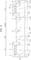
- Fig. 3 is a plan view of a main part of the capacitive element in the embodiment.
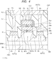
- Fig. 4 is a sectional view of the main part taken along Line X-X in Fig. 3 .
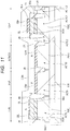
- Fig. 5 is a sectional view of the main part taken along Line Y-Y in Fig. 3 .
- a capacitive element CAP has a configuration in which capacitive elements C1 and C2 are coupled together in parallel.
- Each of the capacitive elements C1 and C2 is coupled to one terminal T1 and the other terminal T2, and a potential V1 is applied to the terminal T1 and a potential V2 to the terminal T2.
- the potential V1 is the ground potential and the potential V2 is an operation power supply potential.
- the structure of the capacitive element CAP will be described with reference to Figs. 3 to 5 .
- the capacitive element CAP is formed, for example, in an n-type well region (n-type semiconductor region) DNW formed in a semiconductor substrate SB, as illustrated in Figs. 3 to 5 .
- the semiconductor substrate SB includes a substrate including p-type single crystal silicon.
- the capacitive element CAP has a structure in which the capacitive element C1 is stacked over the capacitive element C2.
- the capacitive element C1 includes a semiconductor layer (SOI layer) SL, an insulating layer GIH arranged over the semiconductor layer SL, and a conductor layer CLC arranged over the insulating layer GIH.
- the capacitive element C2 includes a p-type well region (p-type semiconductor region) PWC, an insulating layer (buried insulating layer) BOX arranged over the p-type well region PWC, and the semiconductor layer SL arranged over the insulating layer BOX.
- the semiconductor layer SL serves as a common electrode for the capacitive elements C1 and C2.
- Any potential can be applied, independently of the potential of the semiconductor substrate SB, to the p-type well region PWC by interposing the n-type well region DNW between the semiconductor substrate SB and the p-type well region PWC that will be part of the capacitive element CAP.
- the p-type well region PWC which is one electrode of the capacitive element C2, is formed on the side of a main surface SBa of the semiconductor substrate SB, and active regions ACTC1 and ACTC2, the peripheries of which are surrounded by an element isolation layer (element isolation region) IR, are formed in the p-type well region PWC.
- the p-type well region PWC is formed to include the active regions ACTC1 and ACTC2, as illustrated in Fig. 3 .
- the p-type well region PWC is formed to be deeper than the element isolation layer IR and to straddle the active regions ACTC1 and ACTC2, as illustrated in Fig. 4 .
- the active region ACTC1 is sandwiched by two active regions ACTC2, and the capacitive elements C1 and C2 are formed in the active region ACTC1.
- the active region ACTC2 is a terminal coupling part of the p-type well region PWC.
- the active regions ACTC1 and ACTC2 are indicated by thick lines, and the insides of the thick lines (regions surrounded by the thick lines) are the active regions and the outside thereof (region other than the regions surrounded by the thick lines) is the element isolation layer (element isolation region) IR.
- the periphery of each of the active regions ACTC1 and ACTC2 is surrounded by the element isolation layer IR.
- the semiconductor layer SL and the insulating layer BOX are formed, but they are not formed in the two active regions ACTC2.
- a p-type semiconductor region (p-type high-concentration semiconductor region) PH is formed in the main surface SBa of the semiconductor substrate SB.
- a silicide layer SC is formed over the p-type semiconductor region PH, and the silicide layer SC is electrically coupled to a wiring (metal wiring) M1 which is the terminal T2, via a plug electrode PG.
- the silicide layer SC is not illustrated in Fig. 3 .
- the active region means a region defined by the element isolation layer IR in the main surface SBa of the semiconductor substrate SB; however, in the case where the semiconductor layer SL is formed over the main surface SBa of the semiconductor substrate SB, like, for example, the active region ACTC1, a region defined by the element isolation layer IR in a main surface SLa of the semiconductor layer SL is also included.
- the dielectric layer of the capacitive element C2 is comprised of the insulating layer BOX.
- This insulating layer BOX is formed over the p-type well region PWC, in other words, over the main surface SBa of the semiconductor substrate SB.
- the periphery (entire periphery) of the insulating layer BOX is surrounded by the element isolation layer IR, and a side wall BOXs of the insulating layer BOX is in contact with the element isolation layer IR.
- the insulating layer BOX includes, for example, a silicon oxide layer and has a thickness of approximately 10 to 30 nm.
- the semiconductor layer SL is formed over the insulating layer BOX and the periphery (entire periphery) thereof is surrounded by the element isolation layer IR.
- a side wall SLs of the semiconductor layer SL is in contact with the element isolation layer IR.
- the semiconductor layer SL is a p-type single crystal silicon layer into which p-type impurities have been introduced, and has a thickness of, for example, approximately 5 to 25 nm.
- the semiconductor layer SL is a p-type semiconductor layer.
- the dielectric layer of the capacitive element C1 is comprised of the insulating layer GIH.
- the insulating layer GIH includes, for example, a silicon oxide layer and has a thickness of approximately 5 to 15 nm.
- the conductor layer CLC is formed over the insulating layer GIH.
- the conductor layer CLC includes, for example, a polysilicon layer into which p-type impurities have been introduced, and has a thickness of approximately 30 to 200 nm.
- the silicide layer SC is formed over the main surface (surface on the upper side in Fig. 4 ) of the p-type conductor layer CLC, and the conductor layer CLC is electrically coupled to the wiring M1 which is the terminal T2, via the silicide layer SC and the plug electrode PG.
- the semiconductor layer SL, the insulating layer GIH, and the conductor layer CLC have widths substantially equal to each other in the X direction, and each of the insulating layer GIH and the conductor layer CLC covers the entire region of the main surface SLa of the semiconductor layer SL in the X direction.
- a sidewall insulating layer (sidewall spacer) SW is formed over the side walls of the insulating layer GIH and the conductor layer CLC.
- the sidewall insulating layer SW includes an insulating layer, such as a silicon oxide layer, a silicon nitride layer, or a laminated film of a silicon oxide layer and a silicon nitride layer, and reduces a leakage current between the conductor layer CLC and the semiconductor layer SL.
- a structure may be adopted in which the width of the conductor layer CLC (and the insulating layer GIH) is made larger than that of the semiconductor layer SL in the X direction, so that the conductor layer CLC extends (rides) over the element isolation layers IR positioned on both sides of the semiconductor layer SL.
- a leakage current between the conductor layer CLC and the semiconductor layer SL can be further reduced. That is, even if the side wall of the insulating layer GIH is recessed inward with respect to the side wall of the conductor layer CLC (referred to as "undercut"), a leakage current between the conductor layer CLC and the semiconductor layer SL can be further reduced by adopting the above structure.
- the insulating layer GIH and the conductor layer CLC have widths equal to each other in the Y direction, the widths thereof being smaller than that of the semiconductor layer SL.
- the semiconductor layer SL has both a covered region covered with the insulating layer GIH and the conductor layer CLC and an exposed region exposed from the insulating layer GIH, the conductor layer CLC, and the sidewall insulating layer SW.
- the covered region serves as a capacitive part of the capacitive element C1, while the exposed region serves as a terminal coupling part of the semiconductor layer SL. That is, in the exposed region, the p-type semiconductor region PH is formed in the semiconductor layer SL.
- the silicide layer SC is formed over the p-type semiconductor region PH, and the silicide layer SC is coupled to the wiring (metal wiring) M1 which is the terminal T1, via the plug electrode PG.
- the semiconductor device according to the present embodiment has the following characteristics.
- the capacitive element CAP has a structure in which the capacitive element C1 is stacked over the capacitive element C2 and the capacitive element C1 includes the semiconductor layer (SOI layer) SL, the insulating layer GIH arranged over the semiconductor layer SL, and the conductor layer CLC arranged over the insulating layer GIH.
- the capacitive element C2 includes the p-type well region (p-type semiconductor region) PWC, the insulating layer (buried insulating layer) BOX arranged over the p-type well region PWC, and the semiconductor layer SL arranged over the insulating layer BOX. Further, the semiconductor layer SL serves as a common electrode for the capacitive elements C1 and C2.
- the capacitance value per unit area of the capacitive element CAP can be improved without an increase in the manufacturing cost of a semiconductor device and a decrease in the manufacturing yield thereof, whereby the performance of the semiconductor device can be improved.
- Fig. 17 is a view illustrating a C-V characteristic that is a relationship between the capacitance value of a capacitive element and a voltage.
- the C-V characteristic in the case (a) where the impurity concentration of the conductor layer CLC is high and that in the case (b) where the impurity concentration of the conductor layer CLC is low are compared with each other, in the capacitive element C1 in which the conductor layer CLC is formed of a p-type polysilicon layer.
- the capacitance value of a storage region (negative voltage side) can be improved more than in the case of (b).
- the p-type well region PWC which forms the capacitive element C2
- a semiconductor layer semiconductor region containing a high concentration of impurities
- the capacitance characteristic e.g., C-V characteristic showing the relationship between a capacitance value and a voltage
- the high concentration means that it is higher, for example, than the impurity concentration of the semiconductor layer SL.
- Fig. 18 is a view illustrating a C-V characteristic that is a relationship between the capacitance value of a capacitive element and a voltage.
- the C-V characteristic in the case (c) where the conductor layer CLC and the semiconductor layer SL are of the same conductivity type and that in the case (d) where they are of different conductivity types are compared with each other in the capacitive element C1.
- the variation of the capacitance value up to approximately 0 V can be made smaller on the negative voltage side than in the case of (d).
- the semiconductor device according to the embodiment includes the capacitive element CAP, a nonvolatile memory cell MONOS (Metal Oxide Nitride Oxide Silicon), a high breakdown voltage MISFET, and a low breakdown voltage MISFET.
- the high breakdown voltage MISFET and the low breakdown voltage MISFET have a CMOS configuration, but herein description will be given by taking a p-channel type high breakdown voltage MISFET and an n-channel type low breakdown voltage MISFET as an example.
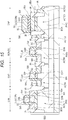
- Figs. 6 to 16 are sectional views of a main part during the manufacturing steps of the semiconductor device according to the embodiment. With reference to Figs.
- the substrate SB2 includes the semiconductor substrate SB, the insulating layer (buried insulating layer) BOX formed over the semiconductor substrate SB, and the semiconductor layer (SOI layer) SL formed over the insulating layer BOX.
- the insulating layer BOX is interposed between the semiconductor substrate SB and the semiconductor layer SL in the entire region of the main surface SBa of the semiconductor substrate SB.
- the semiconductor substrate SB is a layer including p-type single crystal silicon, and has the main surface SBa and a back surface SBb facing the main surface SBa.
- the insulating layer BOX includes, for example, a silicon oxide layer and has a thickness of approximately 10 to 30 nm.
- the semiconductor layer SL is a layer including single crystal silicon and has a thickness of approximately 5 to 25 nm.
- the element isolation layer (element isolation region) IR is formed as illustrated in Fig. 7 .
- the insulating film other than the opening portion is selectively removed by, for example, a CMP (Chemical Mechanical Polishing) process, whereby the element isolation layer IR is selectively formed in the opening.
- CMP Chemical Mechanical Polishing
- the active regions ACTC1 and ACTC2 are formed in a region where the capacitive element CAP is to be formed, an active region ACTM is formed in a region where the nonvolatile memory cell MONOS is to be formed, an active region ACTH is formed in a region where the high breakdown voltage MISFET (HVP) is to be formed, and an active region ACTL is formed in a region where the low breakdown voltage MISFET (LVN) is to be formed, respectively.
- HVP high breakdown voltage MISFET
- LPN low breakdown voltage MISFET
- the active regions ACTC1, ACTC2, ACTM, ACTH, and ACTL are defined by the element isolation layer IR in the main surface SBa of the semiconductor substrate SB and the main surface SLa of the semiconductor layer SL.
- the opening does not reach the back surface SBb of the semiconductor substrate SB.
- it is shallower than the p-type well region PWC described with reference to Fig. 4 .
- the main surface SBa of the semiconductor substrate SB is exposed in the active regions ACTC2, ACTM, and ACTH by removing the semiconductor layer SL and the insulating layer BOX, as illustrated in Fig. 8 .
- the semiconductor layer SL and the insulating layer BOX are left in the active regions ACTC1 and ACTL.
- the n-type well region (n-type semiconductor region) DNW, the n-type well region (n-type semiconductor region) NW, and the p-type well regions (p-type semiconductor regions) PWC, PWM and PWL are formed as illustrated in Fig. 9 .
- the n-type well region DNW is formed by ion implanting n-type impurities, such as phosphorus (P) or arsenic (As), into the semiconductor substrate SB.
- n-type well region DNW is formed to include the active regions ACTC1, ACTC2, ACTM, ACTH, and ACTL.
- the n-type well region DNW is deeper than the p-type well regions PWC, PWM, and PWL.
- the p-type well regions PWC, PWM, and PWL are formed by ion implanting p-type impurities, such as boron (B), into the semiconductor substrate SB.
- p-type impurities such as boron (B)
- the p-type impurities are also implanted into the semiconductor layer SL in the active regions ACTC1 and ACTL, and hence the semiconductor layer SL becomes a p-type semiconductor layer (p-type semiconductor region). That is, the semiconductor layer SL, the other electrode of the capacitive element C2, is formed.
- the p-type well region PWC is formed to include the active regions ACTC1 and ACTC2, and serves as the one electrode of the capacitive element C2 (see Fig. 4 ).
- each of the p-type well regions PWC, PWM, and PWL may have an impurity concentration different from those of the others by being formed in an ion implantation step different from the other implantation steps.
- the p-type well region PWM is formed to have a relatively low impurity concentration because it is a region where the high breakdown voltage MISFET (MONOS) is to be formed, but it is preferable that the p-type well region PWC is formed to have a relatively high impurity concentration for preventing depletion.
- the well formation step described with reference to Fig. 9 may be performed before the step of removing the semiconductor layer SL and the insulating layer BOX described with reference to Fig. 8 .
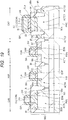
- the insulating layer GIH (gate insulating layer) is formed over both the semiconductor layer SL in the active region ACTC1 and the main surface SBa of the active region ACTH, the insulating layer GIM is formed over the main surface SBa of the active region ACTM, and the insulating layer GIL (gate insulating layer) is formed over the semiconductor layer SL in the active region ACTL, as illustrated in Fig. 10 .
- the insulating layer GIH becomes the gate insulating layer of the high breakdown voltage MISFET (HVP), and serves as the dielectric layer of the capacitive element C1, as described with reference to Fig. 4 .
- the insulating film GIH is used for the dielectric layer of the capacitive element C1 is to reduce a leakage current between the semiconductor layer SL and the conductor layer CLC of the capacitive element C1.
- the insulating layer GIH includes, for example, a silicon oxide layer, and the thickness thereof is approximately 5 to 15 nm.
- the insulating layer GIL becomes the gate insulating layer of the low breakdown voltage MISFET (LVN) and includes, for example, a silicon oxide layer, and the thickness thereof is approximately 1 to 4 nm. That is, the thickness of the insulating layer GIH is larger than that of the insulating layer GIL.
- the insulating layer (gate insulating layer) GIM has a laminated structure of insulating layers (gate insulating layers) GIM1, GIM2, and GIM3.
- the insulating layer GIM1 includes, for example, a silicon oxide layer and has a thickness of approximately 1 to 3 nm
- the insulating layer GIM2 includes, for example, a silicon nitride layer and has a thickness of approximately 5 to 13 nm
- the insulating layer GIM3 includes, for example, a silicon oxide layer and has a thickness of approximately 2 to 4 nm.
- the insulating layer GIM2 is the charge retention layer of the nonvolatile memory cell MONOS.
- a conductor layer CON including, for example, a polysilicon layer (silicon layer) is formed over the substrate SB2, as illustrated in Fig. 11 . That is, the conductor layer CON is formed over the insulating films GIH, GIM, and GIL.
- the thickness of the conductor layer CON is set, for example, to approximately 30 to 200 nm.
- a p-type conductor layer CON is formed by implanting p-type impurities, such as, for example, boron (B), into the conductor layer CON in a region where the capacitive element CAP and the high breakdown voltage MISFET (HVP) are to be formed; and an n-type conductor layer CON is formed by implanting n-type impurities, such as, for example, phosphorus (P) or arsenic (As), into a region where the nonvolatile memory cell MONOS and the low breakdown voltage MISFET (LVN) are to be formed.
- p-type impurities such as, for example, boron (B)
- HVP high breakdown voltage MISFET
- the conductor layer CLC (see Fig. 4 ) that is the other electrode of the capacitive element C1, a conductor layer CLM that is the gate electrode of the nonvolatile memory cell MONOS, a conductor layer CLH that is the gate electrode of the high breakdown voltage MISFET (HVP), and a conductor layer CLL that is the gate electrode of the low breakdown voltage MISFET (LVN) are formed by patterning the conductor layer CON with the use of a photolithography technique and an etching technique, as illustrated in Fig. 12 . As illustrated in Fig. 12 , the width of the conductor layer CLC is equal to that of the active region ACTC1.
- the insulating layer GIH located thereunder is also etched by over-etching, but there is the possibility that at that time the above-mentioned "undercut” may be generated in the insulating layer GIH. If the "undercut” is generated, there is the concern that a leakage current between the conductor layer CLC and the semiconductor layer SL may be increased, and hence it is preferable to adopt a configuration in which both ends of the conductor layer CLC are caused to extend over the element isolation layer IR by making the width of the conductor layer CLC larger than that of the active region ACTC1.
- an n-type semiconductor region (n-type low-concentration semiconductor region) EXN is formed in each of the region (active region ACTM) where the nonvolatile memory cell MONOS is to be formed and the region (active region ACTL) where the low breakdown voltage MISFET (LVN) is to be formed, and a p-type semiconductor region (p-type low-concentration semiconductor region) EXP is formed in the region (active region ACTH) where the high breakdown voltage MISFET (HVP) is to be formed, as illustrated in Fig. 13 .
- a pair of the n-type semiconductor regions EXN are formed in the semiconductor substrate SB (in other words, the p-type well region PWM) on both sides of the conductor layer CLM that is a gate electrode so as to sandwich the conductor layer CLM.
- the semiconductor substrate SB in other words, the p-type well region PWM
- a pair of the n-type semiconductor regions EXN are formed in the semiconductor layer SL on both sides of the conductor layer CLL that is a gate electrode so as to sandwich the conductor layer CLL.
- a pair of the p-type semiconductor regions EXP are formed in the semiconductor substrate SB (in other words, the n-type well region NW) on both sides of the conductor layer CLH that is a gate electrode so as to sandwich the conductor layer CLH.
- the n-type semiconductor region EXN is formed by ion implanting n-type impurities, such as phosphorus (P) or arsenic (As), into the semiconductor substrate SB or the semiconductor layer SL, while the p-type semiconductor region EXP is formed by ion implanting p-type impurities, such as boron (B), into the semiconductor substrate SB.
- n-type impurities such as phosphorus (P) or arsenic (As
- p-type semiconductor region EXP is formed by ion implanting p-type impurities, such as boron (B), into the semiconductor substrate SB.
- the ion implantation for forming the n-type semiconductor region EXN in the region where the nonvolatile memory cell MONOS is to be formed, and the ion implantation for forming the n-type semiconductor region EXN in the region where the low breakdown voltage MISFET (LVN) is to be formed, may or may not be performed in the same step. When
- the sidewall insulating layer (sidewall spacer) SW is formed over the side walls of the conductor layer CLC and the insulating film GIH in the region where the capacitive element CAP is to be formed, as illustrated in Fig. 14 .
- the sidewall insulating film SW is formed by depositing an insulating film for forming the sidewall insulating film SW over the substrate SB2 and by subjecting the insulating film to anisotropic dry etching.
- the insulating film a silicon oxide layer, a silicon nitride layer, a laminated film of a silicon oxide layer and a silicon nitride layer, or the like can be used.
- the sidewall insulating film SW is formed over the side walls of the conductor layer CLM and the insulating film GIM in the region where the nonvolatile memory cell MONOS is to be formed, over the side walls of the conductor layer CLH and the insulating film GIH in the region where the high breakdown voltage MISFET (HVP) is to be formed, and over the side walls of the conductor layer CLL and the insulating film GIL in the region where the low breakdown voltage MISFET (LVN) is to be formed.
- HVP high breakdown voltage MISFET
- the n-type semiconductor region (n-type high-concentration semiconductor region) NH is formed in each of the region (active region ACTM) where the nonvolatile memory cell MONOS is to be formed and the region (active region ACTL) where the low breakdown voltage MISFET (LVN) is to be formed
- the p-type semiconductor region (p-type high-concentration semiconductor region) PH is formed in each of the region (active region ACTH) where the high breakdown voltage MISFET (HVP) is to be formed and the active region ACTC2 of the region where the capacitive element CAP is to be formed, as illustrated in Fig. 14 .
- the n-type semiconductor region NH is formed by ion implanting n-type impurities, such as phosphorus (P) or arsenic (As), into the semiconductor substrate SB or the semiconductor layer SL, while the p-type semiconductor region PH is formed by ion implanting p-type impurities, such as boron (B), into the semiconductor substrate SB.
- n-type impurities such as phosphorus (P) or arsenic (As
- a pair of the n-type semiconductor regions NH are formed in the semiconductor substrate SB (in other words, the p-type well region PWM) on both sides of the conductor layer CLM that is a gate electrode and the sidewall insulating film SW so as to sandwich the conductor layer CLM and the sidewall insulating film SW.
- the semiconductor substrate SB in other words, the p-type well region PWM
- the low breakdown voltage MISFET (LVN) is to be formed
- a pair of the n-type semiconductor regions NH are formed in the semiconductor layer SL on both sides of the conductor layer CLL that is a gate electrode and the sidewall insulating film SW so as to sandwich the conductor layer CLL and the sidewall insulating film SW.
- a pair of the p-type semiconductor regions PH are formed in the semiconductor substrate SB (in other words, the n-type well region NW) on both sides of the conductor layer CLH that is a gate electrode and the sidewall insulating film SW so as to sandwich the conductor layer CLH and the sidewall insulating film SW.
- the p-type semiconductor region (p-type high-concentration semiconductor region) PH is formed in the semiconductor substrate SB (in other words, the p-type well region PWC) .
- the silicide layer SC includes, for example, cobalt silicide (CoSi), nickel silicide (NiSi), or nickel platinum silicide (NiPtSi).
- an interlayer insulating layer IL1 is formed over the substrate SB 2, as illustrated in Fig. 16 .
- the interlayer insulating layer IL1 is formed to cover the conductor layers CLC, CLM, CLH, and CLL, the sidewall insulating film SW, and the like.
- a silicon oxide layer or a laminated film of a silicon nitride layer and a silicon oxide layer located thereover can be used.
- a plurality of contact holes (openings) CNT are provided in the interlayer insulating layer IL, so that the plug electrode PG is formed in the contact hole CNT.
- the contact hole CNT partially exposes the silicide layer SC formed over the surface of the conductor layer CLC and that formed over the surface of the p-type semiconductor region PH.
- the contact hole CNT partially exposes the silicide layer SC formed over the surface of the p-type semiconductor region PH formed in the semiconductor layer SL, as can be seen from Fig. 5 .
- the silicide layer SC over the surface of the n-type semiconductor region NH is partially exposed.
- the silicide layer SC over the surface of the p-type semiconductor region PH is partially exposed.
- the plug electrode PG is formed in the contact hole CNT.
- the plug electrode PG is a conductive member including tungsten (W), and specifically it is comprised of a laminated film of a barrier conductor layer of titanium nitride (TiN) or the like and a tungsten layer located thereover.
- an interlayer insulating layer IL2 is formed over the interlayer insulating layer IL1 in which the plug electrode PG is buried. Then, a wiring groove is formed in the interlayer insulating layer IL2, and thereafter the wiring (metal wiring) M1 is formed in the wiring groove.
- the interlayer insulating layer IL2 includes, for example, a silicon oxide layer.
- the wiring M1 is, for example, a copper wiring containing copper as a main component.
- the conductor layer CLC and the p-type semiconductor region PH are coupled to the wiring M1 via the silicide layer SC and the plug electrode PG, as illustrated in Fig. 16 .
- the n-type semiconductor region NH is coupled to the wiring M1 via the silicide layer SC and the plug electrode PG.
- the p-type semiconductor region PH is coupled to the wiring M1 via the silicide layer SC and the plug electrode PG.
- the wirings in the second or subsequent layers are formed by a dual damascene process or the like, but illustration and description thereof are omitted herein.
- the low breakdown voltage MISFET is a MISFET formed in the semiconductor layer SL arranged over the main surface SBa of the semiconductor substrate SB and via the insulating layer BOX, and is referred to as an SOTB (Silicon On Thin Buried oxide) transistor.
- This low breakdown voltage MISFET (LVN) supplies a desired potential to the p-type well region PWL (referred to as a "back gate”) formed in the main surface SBa of the semiconductor substrate SB via the thin insulating layer BOX, and has the characteristic that a leakage current in the low breakdown voltage MISFET (LVN) can be reduced.
- the high breakdown voltage MISFET (HVP) and the nonvolatile memory cell MONOS are formed in the semiconductor substrate SB, not in the semiconductor layer SL, because high voltage is required for the operation thereof.
- the capacitive element CAP has a structure in which the capacitive elements C1 and C2 are stacked together, and the capacitive element C2 is comprised of the p-type well region PWC that is one electrode, the insulating layer BOX that is a dielectric layer, and the semiconductor layer SL that is the other electrode.
- the capacitive element C1 is comprised of the semiconductor layer SL that is one electrode, the insulating layer GIH that is a dielectric layer, and the conductor layer CLC that is the other electrode, and is formed above the capacitive element C2.
- the other electrode (conductor layer CLC) of the capacitive element C1 is formed by using the conductor layer CON that is the same as the conductor layer CLL that is the gate electrode of the low breakdown voltage MISFET (LVN); the dielectric layer (insulating layer GIH) is formed by using the insulating layer GIH that is the gate insulating layer of the high breakdown voltage MISFET (HVP); and the one electrode (semiconductor layer SL) is formed by using the semiconductor layer SL that is the channel layer of the low breakdown voltage MISFET (LVN) .
- the dielectric layer (insulating layer BOX) of the capacitive element C2 is formed by using the above-mentioned thin insulating layer BOX, and the one electrode (p-type well region PWC) is formed by using the p-type well region PWL ("back gate") of the low breakdown voltage MISFET (LVN). That is, the capacitive element CAP having a stacked structure is formed by using the manufacturing steps for both the low breakdown voltage MISFET (LVN) that is an SOTB transistor and the high breakdown voltage MISFET (HVP). That is, the capacitive element CAP can be formed without an increase in the number of the manufacturing steps.
- the capacitive element C1 is comprised of the p-type semiconductor layer SL, the insulating layer GIH, and the p-type conductor layer CLC, while the capacitive element C2 is comprised of the p-type well region PWC, the insulating layer BOX, and the p-type semiconductor layer SL.
- the capacitive element C1 may be comprised of the n-type semiconductor layer SL, the insulating layer GIH, and the n-type conductor layer CLC, while the capacitive element C2 may be comprised of the n-type well region, the insulating layer BOX, and the n-type semiconductor layer SL.
- Fig. 19 is a sectional view of a main part illustrating the configuration of a semiconductor device according to First Variation.
- the dielectric layer of the capacitive element C1 is formed of the insulating layer GIH that is the gate insulating layer of the high breakdown voltage MISFET (HVP), but in First Variation it is formed of the insulating layer GIM that is the gate insulating layer of the nonvolatile memory cell MONOS. Since the insulating layer GIM includes a silicon nitride layer having a relative permittivity higher than that of a silicon oxide layer, the capacitance value of the capacitive element C1 can be increased.
- Fig. 20 is a sectional view of a main part illustrating the configuration of a semiconductor device according to Second Variation.
- the nonvolatile memory cell MONOS and the high breakdown voltage MISFET (HVP) are formed in the semiconductor substrate SB, but in Second Variation they are formed in the semiconductor layer SL over the insulating layer BOX.
- the conductor layer CLM which is the gate electrode of the nonvolatile memory cell MONOS, is formed over the semiconductor layer SL and via the insulating layer GIM that is a gate insulating layer, and the n-type semiconductor regions EXN and NH, which are respectively a source region and a drain region, are formed in the semiconductor layer SL.
- the conductor layer CLH which is the gate electrode of the high breakdown voltage MISFET (HVP) is formed over the semiconductor layer SL and via the insulating layer GIH that is a gate insulating layer, and the p-type semiconductor regions EXP and PH, which are respectively a source region and a drain region, are formed in the semiconductor layer SL.
- HVP high breakdown voltage MISFET
Landscapes
- Semiconductor Memories (AREA)
- Metal-Oxide And Bipolar Metal-Oxide Semiconductor Integrated Circuits (AREA)
- Engineering & Computer Science (AREA)
- Power Engineering (AREA)
- Semiconductor Integrated Circuits (AREA)
- Non-Volatile Memory (AREA)
- Internal Circuitry In Semiconductor Integrated Circuit Devices (AREA)
Applications Claiming Priority (1)
| Application Number | Priority Date | Filing Date | Title |
|---|---|---|---|
| JP2017089300A JP6867223B2 (ja) | 2017-04-28 | 2017-04-28 | 半導体装置およびその製造方法 |
Publications (2)
| Publication Number | Publication Date |
|---|---|
| EP3442031A2 true EP3442031A2 (fr) | 2019-02-13 |
| EP3442031A3 EP3442031A3 (fr) | 2019-04-17 |
Family
ID=61563173
Family Applications (1)
| Application Number | Title | Priority Date | Filing Date |
|---|---|---|---|
| EP18159566.1A Withdrawn EP3442031A3 (fr) | 2017-04-28 | 2018-03-01 | Dispositif à semi-conducteur et son procédé de fabrication |
Country Status (6)
| Country | Link |
|---|---|
| US (2) | US10490496B2 (fr) |
| EP (1) | EP3442031A3 (fr) |
| JP (1) | JP6867223B2 (fr) |
| KR (1) | KR102463248B1 (fr) |
| CN (1) | CN108807390B (fr) |
| TW (1) | TWI762622B (fr) |
Families Citing this family (8)
| Publication number | Priority date | Publication date | Assignee | Title |
|---|---|---|---|---|
| JP6867223B2 (ja) * | 2017-04-28 | 2021-04-28 | ルネサスエレクトロニクス株式会社 | 半導体装置およびその製造方法 |
| US11495554B2 (en) | 2019-11-01 | 2022-11-08 | Empower Semiconductor, Inc. | Configurable capacitor |
| US11264244B2 (en) * | 2020-02-18 | 2022-03-01 | Renesas Electronics Corporation | Method of manufacturing semiconductor device |
| EP4007001A1 (fr) * | 2020-11-30 | 2022-06-01 | NXP USA, Inc. | Condensateurs intégrés dans un circuit intégré |
| CN113690173B (zh) * | 2021-09-07 | 2024-04-05 | 长江存储科技有限责任公司 | 三维存储器及其制备方法 |
| FR3139234A1 (fr) * | 2022-08-31 | 2024-03-01 | Stmicroelectronics Sa | Protection contre des décharges électrostatiques |
| TW202517058A (zh) * | 2023-10-03 | 2025-04-16 | 聯華電子股份有限公司 | 記憶體結構及其製造方法 |
| WO2025122182A1 (fr) * | 2023-12-06 | 2025-06-12 | Silicon Storage Technology, Inc. | Procédé de fabrication de cellules mémoire, dispositifs transistor et dispositifs logiques sur substrat de silicium isolant |
Citations (1)
| Publication number | Priority date | Publication date | Assignee | Title |
|---|---|---|---|---|
| JP2009010281A (ja) | 2007-06-29 | 2009-01-15 | Renesas Technology Corp | 半導体装置およびその製造方法 |
Family Cites Families (15)
| Publication number | Priority date | Publication date | Assignee | Title |
|---|---|---|---|---|
| US5293059A (en) * | 1987-09-07 | 1994-03-08 | Oki Electric Industry Co., Ltd. | MOS semiconductor device with double-layer gate electrode structure |
| JPH104146A (ja) * | 1996-06-14 | 1998-01-06 | Nippon Steel Corp | 半導体装置及びその製造方法 |
| JP4860058B2 (ja) * | 2001-06-08 | 2012-01-25 | 株式会社半導体エネルギー研究所 | D/a変換回路及び半導体装置 |
| US7112847B1 (en) * | 2003-09-03 | 2006-09-26 | Advanced Micro Devices, Inc. | Smooth fin topology in a FinFET device |
| JP2006303377A (ja) * | 2005-04-25 | 2006-11-02 | Renesas Technology Corp | 半導体装置 |
| US8067803B2 (en) * | 2008-10-16 | 2011-11-29 | Micron Technology, Inc. | Memory devices, transistor devices and related methods |
| WO2010082328A1 (fr) * | 2009-01-15 | 2010-07-22 | ルネサスエレクトロニクス株式会社 | Dispositif à semi-conducteurs et son procédé de fabrication |
| US9385088B2 (en) * | 2009-10-12 | 2016-07-05 | Monolithic 3D Inc. | 3D semiconductor device and structure |
| US8513723B2 (en) * | 2010-01-19 | 2013-08-20 | International Business Machines Corporation | Method and structure for forming high performance MOS capacitor along with fully depleted semiconductor on insulator devices on the same chip |
| JP5558336B2 (ja) * | 2010-12-27 | 2014-07-23 | 株式会社東芝 | 半導体装置 |
| JP2015118972A (ja) * | 2013-12-17 | 2015-06-25 | シナプティクス・ディスプレイ・デバイス合同会社 | 半導体装置の製造方法 |
| US9800204B2 (en) * | 2014-03-19 | 2017-10-24 | Stmicroelectronics International N.V. | Integrated circuit capacitor including dual gate silicon-on-insulator transistor |
| JP6345107B2 (ja) * | 2014-12-25 | 2018-06-20 | ルネサスエレクトロニクス株式会社 | 半導体装置およびその製造方法 |
| JP2017045793A (ja) * | 2015-08-25 | 2017-03-02 | ルネサスエレクトロニクス株式会社 | 半導体装置およびその製造方法 |
| JP6867223B2 (ja) * | 2017-04-28 | 2021-04-28 | ルネサスエレクトロニクス株式会社 | 半導体装置およびその製造方法 |
-
2017
- 2017-04-28 JP JP2017089300A patent/JP6867223B2/ja active Active
-
2018
- 2018-02-24 US US15/904,346 patent/US10490496B2/en active Active
- 2018-03-01 EP EP18159566.1A patent/EP3442031A3/fr not_active Withdrawn
- 2018-04-19 TW TW107113277A patent/TWI762622B/zh active
- 2018-04-25 KR KR1020180047799A patent/KR102463248B1/ko active Active
- 2018-04-26 CN CN201810384325.2A patent/CN108807390B/zh active Active
-
2019
- 2019-10-17 US US16/655,606 patent/US10978385B2/en active Active
Patent Citations (1)
| Publication number | Priority date | Publication date | Assignee | Title |
|---|---|---|---|---|
| JP2009010281A (ja) | 2007-06-29 | 2009-01-15 | Renesas Technology Corp | 半導体装置およびその製造方法 |
Also Published As
| Publication number | Publication date |
|---|---|
| CN108807390B (zh) | 2023-08-08 |
| JP2018190757A (ja) | 2018-11-29 |
| US20180315702A1 (en) | 2018-11-01 |
| US10490496B2 (en) | 2019-11-26 |
| US10978385B2 (en) | 2021-04-13 |
| TW201907547A (zh) | 2019-02-16 |
| KR20180121388A (ko) | 2018-11-07 |
| JP6867223B2 (ja) | 2021-04-28 |
| CN108807390A (zh) | 2018-11-13 |
| EP3442031A3 (fr) | 2019-04-17 |
| KR102463248B1 (ko) | 2022-11-07 |
| TWI762622B (zh) | 2022-05-01 |
| US20200051905A1 (en) | 2020-02-13 |
Similar Documents
| Publication | Publication Date | Title |
|---|---|---|
| US10978385B2 (en) | Semiconductor device and manufacturing method thereof | |
| US9443991B2 (en) | Semiconductor device and method of manufacturing the same | |
| US7968924B2 (en) | Semiconductor device and a method of manufacturing the same | |
| US7883970B2 (en) | Semiconductor device having decoupling capacitor and method of fabricating the same | |
| US9543315B1 (en) | Semiconductor device | |
| US9093319B2 (en) | Semiconductor device and manufacturing method thereof | |
| US10043813B2 (en) | Method of manufacturing semiconductor device | |
| KR970011054B1 (ko) | 반도체 기억장치 및 그 제조방법 | |
| JP6026919B2 (ja) | 半導体装置の製造方法 | |
| US12074205B2 (en) | Transistor structure and related inverter | |
| US20160064402A1 (en) | Method for manufacturing semiconductor device | |
| WO2003069675A1 (fr) | Dispositif a semi-conducteurs et procede de fabrication | |
| US6777758B2 (en) | Semiconductor device | |
| US10056298B2 (en) | Manufacturing method of semiconductor device | |
| US7423324B2 (en) | Double-gate MOS transistor, double-gate CMOS transistor, and method for manufacturing the same |
Legal Events
| Date | Code | Title | Description |
|---|---|---|---|
| PUAI | Public reference made under article 153(3) epc to a published international application that has entered the european phase |
Free format text: ORIGINAL CODE: 0009012 |
|
| AK | Designated contracting states |
Kind code of ref document: A2 Designated state(s): AL AT BE BG CH CY CZ DE DK EE ES FI FR GB GR HR HU IE IS IT LI LT LU LV MC MK MT NL NO PL PT RO RS SE SI SK SM TR |
|
| AX | Request for extension of the european patent |
Extension state: BA ME |
|
| PUAL | Search report despatched |
Free format text: ORIGINAL CODE: 0009013 |
|
| AK | Designated contracting states |
Kind code of ref document: A3 Designated state(s): AL AT BE BG CH CY CZ DE DK EE ES FI FR GB GR HR HU IE IS IT LI LT LU LV MC MK MT NL NO PL PT RO RS SE SI SK SM TR |
|
| AX | Request for extension of the european patent |
Extension state: BA ME |
|
| RIC1 | Information provided on ipc code assigned before grant |
Ipc: H01L 27/08 20060101ALI20190314BHEP Ipc: H01L 27/06 20060101ALI20190314BHEP Ipc: H01L 49/02 20060101ALI20190314BHEP Ipc: H01L 29/94 20060101AFI20190314BHEP |
|
| STAA | Information on the status of an ep patent application or granted ep patent |
Free format text: STATUS: THE APPLICATION IS DEEMED TO BE WITHDRAWN |
|
| 18D | Application deemed to be withdrawn |
Effective date: 20191018 |