EP3442108B1 - Convertisseur de secteur multiniveaux - Google Patents
Convertisseur de secteur multiniveaux Download PDFInfo
- Publication number
- EP3442108B1 EP3442108B1 EP16897950.8A EP16897950A EP3442108B1 EP 3442108 B1 EP3442108 B1 EP 3442108B1 EP 16897950 A EP16897950 A EP 16897950A EP 3442108 B1 EP3442108 B1 EP 3442108B1
- Authority
- EP
- European Patent Office
- Prior art keywords
- circuit
- semiconductor module
- bus
- electric
- capacitor
- Prior art date
- Legal status (The legal status is an assumption and is not a legal conclusion. Google has not performed a legal analysis and makes no representation as to the accuracy of the status listed.)
- Active
Links
Images






Classifications
-
- H—ELECTRICITY
- H10—SEMICONDUCTOR DEVICES; ELECTRIC SOLID-STATE DEVICES NOT OTHERWISE PROVIDED FOR
- H10W—GENERIC PACKAGES, INTERCONNECTIONS, CONNECTORS OR OTHER CONSTRUCTIONAL DETAILS OF DEVICES COVERED BY CLASS H10
- H10W44/00—Electrical arrangements for controlling or matching impedance
- H10W44/601—Capacitive arrangements
-
- H—ELECTRICITY
- H02—GENERATION; CONVERSION OR DISTRIBUTION OF ELECTRIC POWER
- H02M—APPARATUS FOR CONVERSION BETWEEN AC AND AC, BETWEEN AC AND DC, OR BETWEEN DC AND DC, AND FOR USE WITH MAINS OR SIMILAR POWER SUPPLY SYSTEMS; CONVERSION OF DC OR AC INPUT POWER INTO SURGE OUTPUT POWER; CONTROL OR REGULATION THEREOF
- H02M7/00—Conversion of AC power input into DC power output; Conversion of DC power input into AC power output
- H02M7/003—Constructional details, e.g. physical layout, assembly, wiring or busbar connections
-
- H—ELECTRICITY
- H02—GENERATION; CONVERSION OR DISTRIBUTION OF ELECTRIC POWER
- H02M—APPARATUS FOR CONVERSION BETWEEN AC AND AC, BETWEEN AC AND DC, OR BETWEEN DC AND DC, AND FOR USE WITH MAINS OR SIMILAR POWER SUPPLY SYSTEMS; CONVERSION OF DC OR AC INPUT POWER INTO SURGE OUTPUT POWER; CONTROL OR REGULATION THEREOF
- H02M7/00—Conversion of AC power input into DC power output; Conversion of DC power input into AC power output
- H02M7/42—Conversion of DC power input into AC power output without possibility of reversal
- H02M7/44—Conversion of DC power input into AC power output without possibility of reversal by static converters
- H02M7/48—Conversion of DC power input into AC power output without possibility of reversal by static converters using discharge tubes with control electrode or semiconductor devices with control electrode
- H02M7/483—Converters with outputs that each can have more than two voltages levels
-
- H—ELECTRICITY
- H02—GENERATION; CONVERSION OR DISTRIBUTION OF ELECTRIC POWER
- H02M—APPARATUS FOR CONVERSION BETWEEN AC AND AC, BETWEEN AC AND DC, OR BETWEEN DC AND DC, AND FOR USE WITH MAINS OR SIMILAR POWER SUPPLY SYSTEMS; CONVERSION OF DC OR AC INPUT POWER INTO SURGE OUTPUT POWER; CONTROL OR REGULATION THEREOF
- H02M7/00—Conversion of AC power input into DC power output; Conversion of DC power input into AC power output
- H02M7/42—Conversion of DC power input into AC power output without possibility of reversal
- H02M7/44—Conversion of DC power input into AC power output without possibility of reversal by static converters
- H02M7/48—Conversion of DC power input into AC power output without possibility of reversal by static converters using discharge tubes with control electrode or semiconductor devices with control electrode
- H02M7/483—Converters with outputs that each can have more than two voltages levels
- H02M7/487—Neutral point clamped inverters
-
- H—ELECTRICITY
- H10—SEMICONDUCTOR DEVICES; ELECTRIC SOLID-STATE DEVICES NOT OTHERWISE PROVIDED FOR
- H10W—GENERIC PACKAGES, INTERCONNECTIONS, CONNECTORS OR OTHER CONSTRUCTIONAL DETAILS OF DEVICES COVERED BY CLASS H10
- H10W90/00—Package configurations
Definitions
- the present invention relates to a multilevel power converter.
- a three-level power converter is disclosed in which the circuit inductance in a power conversion circuit is suppressed, ease of maintenance is enhanced and, at the same time, manufacturing costs can be reduced (see PTL 1).
- EP 2 966 768 A1 relates to a configuration of a three-level inverter which enables an improvement in power conversion efficiency and a reduction in the size and cost of a device.
- EP 3 093 974 A1 relates to a three-level power converter that uses a semiconductor switch module, and more particularly to the wiring structures of a capacitor and a module.
- a line portion of a power conversion circuit has a low degree of freedom in regard to length due to physical restrictions. Accordingly, when the inductance in a communication loop, which is generated at the time of turning off switching elements, increases, a surge voltage increases.
- a multilevel power converter is a multilevel power converter in which a power conversion circuit is formed of a plurality of electric circuits, the multilevel power converter including: a first capacitor provided in a positive electrode circuit; a second capacitor connected with the first capacitor in series, and provided in a negative electrode circuit; a first electric circuit formed of a first switching element through which an electric current flows from the positive electrode circuit to an AC circuit, and a first diode connected with the first switching element in anti-parallel; a second electric circuit formed of a second switching element, and a second diode connected with the second switching element in series, the second electric circuit being configured to form an electric path which connects a capacitor circuit formed of the first capacitor and the second capacitor and the AC circuit with each other; a third electric circuit formed of a third switching element, and a third diode connected with the third switching element in series, the third electric circuit being configured to form an electric path which connects the capacitor circuit and the AC circuit with each other, and through which
- Fig. 1 is a configuration diagram showing a configuration of a three-level power converter 20 according to a first embodiment of the present invention.
- Fig. 2 is a circuit diagram showing a configuration of a power conversion circuit of the three-level power converter 20 according to this embodiment.
- identical components are given the same reference characters, and the detailed description of such components is omitted. The description is made primarily with respect to the different components.
- the three-level power converter 20 is a neutral-point-switch-type three-level (multi) level inverter.
- the description is made with respect to the configuration of one of three phases of the power conversion circuit. However, it is assumed that all phases have the same configuration. Further, the description is primarily made with the assumption that the three-level power converter 20 performs reverse conversion from DC power to AC power. However, the three-level power converter 20 may perform rectification from AC power to DC power. Further, the power conversion circuit may have three phases, or may have a single phase.
- the three-level power converter 20 may be a power converter of more than three levels provided that the power converter has a configuration substantially equal to the configuration of this embodiment.
- the three-level power converter 20 includes four semiconductor modules 1, 2, 3, 4, two capacitors 5, 6, and four laminated buses L1, L2, L3, L4.
- the laminated buses L1 to L4 are conductors which are laminated (having a thin-plate shape).
- the AC bus L1 forms an AC circuit of the power conversion circuit, and includes an AC terminal.
- the capacitor bus L2 is connected to the two capacitors 5, 6, and forms a capacitor circuit of the power conversion circuit.
- the positive electrode bus L3 forms a positive electrode circuit of the power conversion circuit, and includes a positive electrode terminal.
- the negative electrode bus L4 forms a negative electrode circuit of the power conversion circuit, and includes a negative electrode terminal.
- the laminated buses L1 to L4 have a rectangular parallelepiped plate shape.
- the AC bus L1 and the capacitor bus L2 have substantially the same shape.
- the positive electrode bus L3 and the negative electrode bus L4 have a shape which is substantially half the shape of the AC bus L1 or the capacitor bus L2. Assume the side on which the semiconductor modules 1 to 4 and the capacitors 5, 6 are mounted as the upper side, the AC bus L1, the capacitor bus L2, the positive electrode bus L3 or the negative electrode bus L4 are stacked in this order from the top.
- the positive electrode bus L3 and the negative electrode bus L4 are disposed adjacent to each other in the lateral direction without overlapping.
- the positive electrode bus L3 and the negative electrode bus L4 are set in one layer. Accordingly, the laminated buses L1 to L4 form three layers in total. Insulation is provided between the respective laminated buses L1 to L4. The order of the laminated buses L1 to L4 to be stacked may be exchanged in any manner.
- the first semiconductor module 1 includes a switching element 11 and a diode 12.
- the diode 12 is connected with the switching element 11 in anti-parallel.
- a collector (input side) of the switching element 11 and a cathode of the diode 12 are connected with each other, and an emitter (output side) of the switching element 11 and an anode of the diode 12 are connected with each other.
- the cathode of the diode 12 is connected to the positive electrode bus L3.
- the anode of the diode 12 is connected to the AC bus L1.
- the switching element 11 is described assuming that the switching element 11 is an IGBT (insulated gate bipolar transistor).
- the switching element 11 may be a switching element of another type such as a MOSFET (metal oxide semiconductor field-effect transistor). Further, other switching elements are described assuming that, in the same manner as the switching element 11, other switching elements are also IGBTs. However, other switching elements may also be switching elements of another type.
- MOSFET metal oxide semiconductor field-effect transistor
- the second semiconductor module 2 includes a switching element 21 and a diode 22.
- the second semiconductor module 2 may further include a diode connected to the switching element 21 in anti-parallel.
- the switching element 21 is connected in series such that the direction of a flowing electric current is equal to the direction of a flowing electric current in the diode 22, and an electric current is inputted into the switching element 21 from the diode 22.
- a collector (input side) of the switching element 21 and a cathode of the diode 22 are connected with each other.
- An anode of the diode 22 is connected to the capacitor bus L2.
- An emitter (output side) of the switching element 21 is connected to the AC bus L1.
- a current path through which an electric current flows from the capacitor circuit to the AC circuit is formed in the electric circuit of the second semiconductor module 2.
- a terminal Tm connected to a line, connecting the switching element 21 and the diode 22 with each other, is exposed to the outside of the second semiconductor module 2.
- the terminal Tm is connected to a terminal Tm of the third semiconductor module 3.
- the third semiconductor module 3 includes a switching element 31 and a diode 32.
- the third semiconductor module 3 may further include a diode connected to the switching element 31 in anti-parallel.
- the switching element 31 is connected in series such that the direction of a flowing electric current is equal to the direction of a flowing electric current in the diode 32, and an electric current is inputted into the switching element 31 from the diode 32.
- a collector (input side) of the switching element 31 and a cathode of the diode 32 are connected with each other.
- An anode of the diode 32 is connected to the AC bus L1. With such a configuration, a current path through which an electric current flows from the AC circuit to the capacitor circuit is formed in the electric circuit of the third semiconductor module 3.
- an electric current flows in the opposite direction to the electric circuit of the second semiconductor module 2.
- An emitter (output side) of the switching element 31 is connected to the capacitor bus L2.
- the terminal Tm connected to a line, connecting the switching element 31 and the diode 32 with each other, is exposed to the outside of the third semiconductor module 3.
- the terminal Tm is connected to the terminal Tm of the second semiconductor module 2.
- the fourth semiconductor module 4 includes a switching element 41 and a diode 42.
- the diode 42 is connected with the switching element 41 in anti-parallel.
- a collector (input side) of the switching element 41 and a cathode of the diode 42 are connected with each other, and an emitter (output side) of the switching element 41 and an anode of the diode 42 are connected with each other.
- the cathode of the diode 42 is connected to the AC bus L1.
- the anode of diode 42 is connected to the negative electrode bus L4.
- the second semiconductor module 2 and the third semiconductor module 3 may be respectively replaced with a second semiconductor module 2a and a third semiconductor module 3a according to a modification of this embodiment which are shown in Fig. 3 .
- the configuration of a switching element 21a and a diode 22a of the second semiconductor module 2a shown in Fig. 3 is obtained by exchanging positions of the switching element 21 and the diode 22 of the second semiconductor module 2 shown in Fig. 2 with each other.
- the configuration of a switching element 31a and a diode 32a of the third semiconductor module 3a shown in Fig. 3 is obtained by exchanging positions of the switching element 31 and the diode 32 of the third semiconductor module 3 shown in Fig. 2 with each other.
- the capacitors 5, 6 have a cylindrical shape.
- the capacitor 5 is a capacitor on the positive electrode side which is provided in the positive electrode circuit.
- the capacitor 6 is a capacitor on the negative electrode side which is provided in the negative electrode circuit.
- the capacitors 5, 6 are connected in series via the capacitor bus L2.
- Each capacitor 5, 6 may be formed of one capacitor, or may be formed of a plurality of unit capacitors.
- the semiconductor modules 1 to 4 and the capacitors 5, 6 are disposed on a surface of the AC bus L1 which is present in an uppermost layer.
- the first semiconductor module 1, the second semiconductor module 2, the third semiconductor module 3, and the fourth semiconductor module 4 are arranged in this order in one lateral line.
- the capacitors 5, 6 are disposed parallel to each other in the lateral direction in a line separate from the semiconductor modules 1 to 4.
- the semiconductor module 1 and the capacitor 5 are elements connected to the positive electrode bus L3 therefore these elements are disposed so as to be positioned above the positive electrode bus L3.
- the semiconductor module 4 and the capacitor 6 are elements connected to the negative electrode bus L4 therefore these elements are disposed so as to be positioned above the negative electrode bus L4.
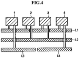
- Fig. 4 is a side cross-sectional view showing a state where semiconductor modules 1 to 4 are respectively connected to the laminated buses L1 to L4.
- the first semiconductor module 1 is wired to the AC bus L1 and to the positive electrode bus L3.
- the AC bus L1 is present in the uppermost layer.
- An AC terminal of the first semiconductor module 1 is connected to a surface of the AC bus L1 disposed below the first semiconductor module 1.
- the positive electrode bus L3 is present in the lowermost layer.
- a positive electrode terminal of the first semiconductor module 1 penetrates the AC bus L1 and the capacitor bus L2, and is connected to the positive electrode bus L3 at a point where the positive electrode terminal reaches the positive electrode bus L3. Accordingly, a hole, which allows the positive electrode terminal of the first semiconductor module 1 to pass therethrough, is respectively formed in the AC bus L1 and the capacitor bus L2 in an overlapping manner. Insulation treatment is applied to these holes so as to prevent short-circuiting even if the positive electrode terminal of the first semiconductor module 1 comes into contact with the holes.
- holes necessary for allowing terminals of other semiconductor modules 2 to 4 to pass therethrough are also formed in the AC bus L1 or the capacitor bus L2.
- Other semiconductor modules 2 to 4 are also wired in the same manner as the first semiconductor module 1.
- the second semiconductor module 2 and the third semiconductor module 3 are wired to the AC bus L1 and to the capacitor bus L2.
- the fourth semiconductor module 4 is wired to the AC bus L1 and to the negative electrode bus L4.
- the second semiconductor module 2 and the third semiconductor module 3 are connected with each other through the terminals Tm.
- the semiconductor modules 1 to 4 are arranged such that the inductance in a circuit, through which a positive electric current flows, is reduced during a period where an AC voltage is zero or a positive AC voltage. With such a configuration, it is possible to reduce the inductance in a communication loop at the time of turning off the switching elements 11, 21, 31, 41 of the respective semiconductor modules 1 to 4. An electric current which flows through the communication loop flows through a path where an electric current flowing out from the AC side of the first semiconductor module 1 enters through the second semiconductor module 2, and through a path where an electric current flowing out from the AC side of the third semiconductor module 3 enters the fourth semiconductor module 4.
- the first semiconductor module 1 is disposed adjacent to the second semiconductor module 2 such that the inductance in a path between the first semiconductor module 1 and the second semiconductor module 2 is reduced.
- the third semiconductor module 3 is disposed adjacent to the fourth semiconductor module 4 such that the inductance in a path between the third semiconductor module 3 and the fourth semiconductor module 4 is reduced.
- the first semiconductor module 1 and the second semiconductor module 2 are disposed adjacent to each other in the lateral direction.
- the first semiconductor module 1 and the second semiconductor module 2 may be disposed adjacent to each other in the vertical direction.
- the third semiconductor module 1 and the fourth semiconductor module 2 may also be disposed adjacent to each other in the vertical direction.
- a three-level power conversion circuit which primarily performs reverse conversion instead of rectification, is formed of four semiconductor modules 1 to 4, the first semiconductor module 1 and the second semiconductor module 2 are disposed adjacent to each other, and the third semiconductor module 3 and the fourth semiconductor module 4 are disposed adjacent to each other.
- the three-level power conversion circuit may be a circuit which does not perform rectification but performs only reverse conversion.
- the positive electrode bus L3 and the negative electrode bus L4 are disposed parallel to each other in the lateral direction without overlapping and hence, the inductance between the positive electrode bus L3 and the negative electrode bus L4 can be increased.
- the elements 11, 12 connected to the positive electrode bus L3 and the elements 41, 42 connected to the negative electrode bus L4 are respectively present in identical semiconductor modules 1, 4, and the semiconductor modules 1, 4 are disposed so as to be positioned above the buses L3, L4 having polarities of the semiconductor modules which are to be connected. With such a configuration, the inductance in the communication loop on the opposite side is increased so that an unnecessary commutating operation can be suppressed.
- the positive electrode bus L3 and the negative electrode bus L4 are disposed parallel to each other in the lateral direction without overlapping and hence, the positive electrode bus L3 and the negative electrode bus L4 can be set in one layer. Accordingly, the three-level power converter can be miniaturized and hence, manufacturing costs can be reduced.
- Fig. 5 is a configuration diagram showing a configuration of a three-level power converter 20A according to a second embodiment of the present invention.
- Fig. 6 is a circuit diagram showing a configuration of a power conversion circuit of the three-level power converter 20A according to this embodiment.
- the three-level power converter 20A is a converter obtained by exchanging positions of the second semiconductor module 2 and the third semiconductor module 3 in the three-level power converter 20 according to the first embodiment. That is, a first semiconductor module 1 and a third semiconductor module 3 are disposed adjacent to each other, and a second semiconductor module 2 and a fourth semiconductor module 4 are disposed adjacent to each other.
- the three-level power converter 20A primarily performs rectification. Other configurations are substantially equal to the corresponding points in the first embodiment.
- the second semiconductor module 2 and the third semiconductor module 3 may be respectively replaced with the second semiconductor module 2a and the third semiconductor module 3a shown in Fig. 3 .
- a three-level power conversion circuit which primarily performs rectification instead of reverse conversion is formed of four semiconductor modules 1 to 4.
- the first semiconductor module 1 and the third semiconductor module 3 are disposed adjacent to each other, and the second semiconductor module 2 and the fourth semiconductor module 4 are disposed adjacent to each other.
- the three-level power conversion circuit may be a circuit which does not perform reverse conversion but performs only rectification.
- Fig. 7 is a configuration diagram showing a configuration of a three-level power converter 20B according to a third embodiment of the present invention.
- Fig. 8 is a circuit diagram showing a configuration of a power conversion circuit of the three-level power converter 20B according to this embodiment.
- the three-level power converter 20B is a converter configured such that, in the three-level power converter 20 according to the first embodiment, a seventh semiconductor module 7 is provided as a substitute for the first semiconductor module 1 and the second semiconductor module 2, and an eighth semiconductor module 8 is provided as a substitute for the third semiconductor module 3 and the fourth semiconductor module 4.
- Other configurations are substantially equal to the corresponding points in the first embodiment.
- the seventh semiconductor module 7 is a module obtained by forming the first semiconductor module 1 and the second semiconductor module 2 according to the first embodiment into one semiconductor module.
- the seventh semiconductor module 7 includes a switching element 11, a diode 12, a switching element 21, and a diode 22.
- An emitter of the switching element 11 is connected to an emitter of the switching element 21.
- the eighth semiconductor module 8 is a module obtained by forming the third semiconductor module 3 and the fourth semiconductor module 4 into one semiconductor module.
- the eighth semiconductor module 8 includes a switching element 31, a diode 32, a switching element 41, and a diode 42.
- An anode of the diode 32 is connected to a collector of the switching element 41.
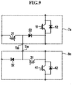
- the seventh semiconductor module 7 and the eighth semiconductor module 8 may be respectively replaced with a seventh semiconductor module 7a and an eighth semiconductor module 8a according to a modification of this embodiment which are shown in Fig. 9 .
- the configurations of a switching element 21a and a diode 22a of the seventh semiconductor module 7a shown in Fig. 9 are equal to corresponding configurations of the second semiconductor module 2a shown in Fig. 3 .
- the configurations of a switching element 31a and a diode 32a of the eighth semiconductor module 8a shown in Fig. 9 are equal to corresponding configurations of the third semiconductor module 3a shown in Fig. 3 .
- the inductance in a communication loop at the time of turning off the switching elements 11 to 41 can be reduced. Accordingly, a surge voltage at the time of turning off the switching elements 11 to 41 can be suppressed.
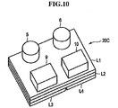
- Fig. 10 is a configuration diagram showing a configuration of a three-level power converter 20C according to a fourth embodiment of the present invention.
- Fig. 11 is a circuit diagram showing a configuration of a power conversion circuit of the three-level power converter 20C according to this embodiment.
- the three-level power converter 20C is a converter configured such that, in the three-level power converter 20A according to the second embodiment, a ninth semiconductor module 9 is provided as a substitute for the first semiconductor module 1 and the third semiconductor module 3, and a tenth semiconductor module 10 is provided as a substitute for the second semiconductor module 2 and the fourth semiconductor module 4.
- Other configurations are substantially equal to the corresponding points in the second embodiment.
- the ninth semiconductor module 9 is a module obtained by forming the first semiconductor module 1 and the third semiconductor module 3 according to the second embodiment into one semiconductor module.
- the ninth semiconductor module 9 includes a switching element 11, a diode 12, a switching element 31, and a diode 32.
- An emitter of the switching element 11 is connected to an anode of the diode 32.
- the tenth semiconductor module 10 is a module obtained by forming the second semiconductor module 2 and the fourth semiconductor module 4 into one semiconductor module.
- the tenth semiconductor module 10 includes a switching element 21, a diode 22, a switching element 41, and a diode 42.
- An emitter of the switching element 21 is connected to a collector of the switching element 41.
- the ninth semiconductor module 9 and the tenth semiconductor module 10 may be respectively replaced with a ninth semiconductor module 9a and a tenth semiconductor module 10a according to a modification of this embodiment which are shown in Fig. 12 .
- the configurations of a switching element 31a and a diode 32a of the ninth semiconductor module 9a shown in Fig. 12 are equal to corresponding configurations of the third semiconductor module 3a shown in Fig. 3 .
- the configurations of a switching element 21a and a diode 22a of the tenth semiconductor module 10a shown in Fig. 12 are equal to corresponding configurations of the second semiconductor module 2a shown in Fig. 3 .
- the ninth semiconductor module 9 and the tenth semiconductor module 10 even if the respective semiconductor modules 9, 10 are disposed at any position, the inductance in a communication loop at the time of turning off the switching elements 11 to 41 can be reduced. Accordingly, a surge voltage at the time of turning off the switching elements 11 to 41 can be suppressed.
Landscapes
- Engineering & Computer Science (AREA)
- Power Engineering (AREA)
- Inverter Devices (AREA)
Claims (8)
- Convertisseur de puissance multi-niveaux dans lequel un circuit de conversion de puissance est formé d'une pluralité de circuits électriques (1, 2, 3, 4),
le convertisseur de puissance multi-niveaux comprenant :un premier condensateur (5) prévu dans un circuit d'électrode positive ;un deuxième condensateur (6) connecté en série au premier condensateur (5), et prévu dans un circuit d'électrode négative ;un premier circuit électrique (1) formé d'un premier élément de commutation (11) à travers lequel un courant électrique circule du circuit d'électrode positive à un circuit CA, et une première diode (12) connectée en antiparallèle au premier élément de commutation (11) ;un deuxième circuit électrique (2) formé d'un deuxième élément de commutation (21), et une deuxième diode (22) connectée en série au deuxième élément de commutation (21), le deuxième circuit électrique (2) étant configuré pour former un trajet électrique qui connecte un circuit de condensateur formé du premier condensateur (5) et le deuxième condensateur (6) et le circuit CA les uns aux autres ;un troisième circuit électrique (3) formé d'un troisième élément de commutation (31), et une troisième diode (32) connectée en série au troisième élément de commutation (31), le troisième circuit électrique (3) étant configuré pour former un trajet électrique qui connecte le circuit de condensateur et le circuit CA l'un à l'autre, et à travers lequel un courant électrique circule dans une direction opposée au deuxième circuit électrique (2) ;un quatrième circuit électrique (4) formé d'un quatrième élément de commutation (41) à travers lequel un courant électrique circule du circuit CA au circuit d'électrode négative, et une quatrième diode (42) connectée en antiparallèle au quatrième élément de commutation (41) ;un bus CA (L1) qui est stratifié, le bus CA formant le circuit CA ;un bus de condensateur (L2) qui est stratifié, le bus de condensateur étant empilé avec le bus CA (L1) et configuré pour former le circuit de condensateur ;un bus d'électrode positive (L3) qui est stratifié, le bus d'électrode positive (L3) étant empilé avec le bus CA (L1) et le bus de condensateur (L2) et configuré pour former le circuit d'électrode positive ; etun bus d'électrode négative (L4) qui est stratifié, le bus d'électrode négative (L4) étant empilé avec le bus CA (L1) et le bus de condensateur (L2) et configuré pour former le circuit d'électrode négative, dans lequelle bus CA (L1), le bus de condensateur (L2), le bus positif (L3) ou le bus négatif (L4) sont empilés les uns sur les autres, de manière à former trois couches au total, le bus d'électrode positive (L3) et le bus d'électrode négative (L4) étant fixés en une seule couche,la pluralité de circuits électriques (1, 2, 3, 4) est agencée de sorte que chacun parmi le premier circuit électrique (1) et le quatrième circuit électrique (4) soit adjacent à l'un ou l'autre du deuxième circuit électrique (2) ou du troisième circuit électrique (3), de manière à réduire l'inductance dans une boucle de communication etles circuits électriques (1, 2, 3, 4) et les condensateurs (5, 6) sont disposés sur une surface du bus CA (L1) qui se trouve dans une couche supérieure, le premier circuit électrique (1), le deuxième circuit électrique (2), le troisième circuit électrique (3), et le quatrième circuit électrique (4) étant agencés dans un ordre défini sur une ligne latérale, les condensateurs (5, 6) étant disposés parallèlement les uns aux autres dans une direction latérale dans une ligne séparée des circuits électriques (1, 2, 3, 4). - Convertisseur de puissance multi-niveaux selon la revendication 1, dans lequel
le bus d'électrode positive (L3) est empilé avec le bus CA (L1) et le bus de condensateur (L2) sans chevauchement avec le bus d'électrode négative (L4). - Convertisseur de puissance multi-niveaux selon la revendication 1, dans lequel le circuit de conversion de puissance est formé d'une pluralité de modules à semi-conducteurs, et dans lequel
la pluralité de modules à semi-conducteurs (1, 2, 3, 4) comporte :un premier module à semi-conducteur dans lequel le premier circuit électrique (1) est formé ;un deuxième module à semi-conducteur dans lequel le deuxième circuit électrique (2) est formé ;un troisième module à semi-conducteur dans lequel le troisième circuit électrique (3) est formé ; etun quatrième module à semi-conducteur dans lequel le quatrième circuit électrique (4) est formé,dans lequelchacun parmi le premier module à semi-conducteur et le quatrième module à semi-conducteur est disposé de manière à être adjacent à l'un ou à l'autre du deuxième module à semi-conducteur ou du troisième module à semi-conducteur. - Convertisseur de puissance multi-niveaux selon la revendication 3, dans lequel
le circuit de conversion de puissance est configuré pour effectuer une opération d'inversion qui convertit une puissance CC en puissance CA,
le deuxième circuit électrique (2) est formé de manière à permettre à un courant électrique de circuler du circuit de condensateur au circuit CA,
le premier module à semi-conducteur est disposé adjacent au deuxième module à semi-conducteur, et
le quatrième module à semi-conducteur est disposé adjacent au troisième module à semi-conducteur. - Convertisseur de puissance multi-niveaux selon la revendication 3, dans lequel
le circuit de conversion de puissance est configuré pour effectuer une opération de conversion qui convertit une puissance CA en puissance CC,
le deuxième circuit électrique (2) est formé de manière à permettre à un courant électrique de circuler du circuit de condensateur au circuit CA,
le premier module à semi-conducteur est disposé adjacent au troisième module à semi-conducteur, et
le quatrième module à semi-conducteur est disposé adjacent au deuxième module à semi-conducteur. - Convertisseur de puissance multi-niveaux selon la revendication 1, dans lequel
la pluralité de modules à semi-conducteurs (1, 2, 3, 4) comporte :un premier module à semi-conducteur (7) dans lequel le premier circuit électrique (1) et le deuxième circuit électrique (2) sont formés ; etun deuxième module à semi-conducteur (8) dans lequel le troisième circuit électrique (3) et le quatrième circuit électrique (4) sont formés. - Convertisseur de puissance multi-niveaux selon la revendication 6, dans lequel
le circuit de conversion de puissance est configuré pour effectuer une opération d'inversion qui convertit une puissance CC en puissance CA, et
le deuxième circuit électrique (2) est formé de manière à permettre à un courant électrique de circuler du circuit de condensateur au circuit CA. - Convertisseur de puissance multi-niveaux selon la revendication 6, dans lequel
le circuit de conversion de puissance est configuré pour effectuer une opération de conversion qui convertit une puissance CA en puissance CC, et
le deuxième circuit électrique (2) est formé de manière à permettre à un courant électrique de circuler du circuit CA au circuit de condensateur.
Applications Claiming Priority (1)
| Application Number | Priority Date | Filing Date | Title |
|---|---|---|---|
| PCT/JP2016/061584 WO2017175394A1 (fr) | 2016-04-08 | 2016-04-08 | Convertisseur de secteur multiniveaux |
Publications (3)
| Publication Number | Publication Date |
|---|---|
| EP3442108A1 EP3442108A1 (fr) | 2019-02-13 |
| EP3442108A4 EP3442108A4 (fr) | 2019-11-20 |
| EP3442108B1 true EP3442108B1 (fr) | 2020-12-30 |
Family
ID=60001065
Family Applications (1)
| Application Number | Title | Priority Date | Filing Date |
|---|---|---|---|
| EP16897950.8A Active EP3442108B1 (fr) | 2016-04-08 | 2016-04-08 | Convertisseur de secteur multiniveaux |
Country Status (6)
| Country | Link |
|---|---|
| US (1) | US10879814B2 (fr) |
| EP (1) | EP3442108B1 (fr) |
| JP (1) | JP6573025B2 (fr) |
| CN (1) | CN109121456B (fr) |
| ES (1) | ES2856875T3 (fr) |
| WO (1) | WO2017175394A1 (fr) |
Cited By (1)
| Publication number | Priority date | Publication date | Assignee | Title |
|---|---|---|---|---|
| EP4425780A1 (fr) * | 2023-03-03 | 2024-09-04 | Infineon Technologies AG | Agencement de semi-conducteur et agencement de module semi-conducteur |
Families Citing this family (6)
| Publication number | Priority date | Publication date | Assignee | Title |
|---|---|---|---|---|
| CN115315892B (zh) | 2020-03-17 | 2026-04-21 | 华为数字能源技术有限公司 | 用于具有改进的共模性能的输入串联结构的转换器系统的ac/dc转换器级 |
| JP7501164B2 (ja) * | 2020-07-02 | 2024-06-18 | 富士電機株式会社 | 電力変換装置 |
| DE102023115709A1 (de) * | 2023-06-15 | 2024-12-19 | Semikron Elektronik Gmbh & Co. Kg | Erstes Leistungshalbleitermodul für eine erste Teilschaltung, zweites Leistungshalbleitermodul für eine zweite Teilschaltung und Anordnung hiermit |
| JP2025144770A (ja) * | 2024-03-21 | 2025-10-03 | 株式会社デンソー | マルチレベルインバータ |
| CN118264079B (zh) * | 2024-03-28 | 2026-02-17 | 漳州科华电气技术有限公司 | 一种多电平电路、印刷电路板和变换器 |
| US20260054579A1 (en) * | 2024-08-22 | 2026-02-26 | BorgWarner US Technologies LLC | Systems for inverter having t-type arrangement for electric vehicle |
Family Cites Families (16)
| Publication number | Priority date | Publication date | Assignee | Title |
|---|---|---|---|---|
| JP5440335B2 (ja) * | 2010-04-06 | 2014-03-12 | 富士電機株式会社 | パワー半導体モジュール及びそれを用いた電力変換装置 |
| JP5724314B2 (ja) * | 2010-11-16 | 2015-05-27 | 富士電機株式会社 | パワー半導体モジュール |
| US9478994B2 (en) * | 2012-07-30 | 2016-10-25 | Obshchestvo S Ogranichennoy Otvetstvennostyu “Sistemy Upravlenia Khraneniem Energii” | Hierarchical system for controlling a battery of electrical energy storage devices |
| JP2014036509A (ja) | 2012-08-09 | 2014-02-24 | Mitsubishi Electric Corp | 3レベル電力変換装置 |
| DE102013104081B3 (de) * | 2013-04-23 | 2014-05-15 | Semikron Elektronik Gmbh & Co. Kg | 3-Level-Stromrichterhalbbrücke |
| CN203504422U (zh) * | 2013-07-29 | 2014-03-26 | 特变电工新疆新能源股份有限公司 | 一种用于t型三电平变流器的叠层母排 |
| JP6086157B2 (ja) | 2013-10-02 | 2017-03-01 | 富士電機株式会社 | 3レベルインバータ |
| JP6268939B2 (ja) * | 2013-11-06 | 2018-01-31 | 株式会社明電舎 | 3レベル電力変換装置 |
| CN103607131B (zh) * | 2013-12-03 | 2016-01-20 | 上海理工大学 | 三电平逆变器中点电位平衡控制方法 |
| CN204031003U (zh) * | 2014-07-31 | 2014-12-17 | 深圳市英威腾电气股份有限公司 | 一种叠层母排及二极管钳位三电平拓扑装置 |
| JP6160780B2 (ja) | 2014-08-26 | 2017-07-12 | 富士電機株式会社 | 3レベル電力変換装置 |
| CN105450042B (zh) | 2014-09-26 | 2018-04-17 | 台达电子工业股份有限公司 | 三电平功率变换器及其功率单元 |
| CN204316350U (zh) * | 2014-12-30 | 2015-05-06 | 深圳市汇川技术股份有限公司 | T型三电平桥臂模块安装结构以及功率变换器 |
| DE102015115271B4 (de) * | 2015-09-10 | 2021-07-15 | Infineon Technologies Ag | Elektronikbaugruppe mit entstörkondensatoren und verfahren zum betrieb der elektronikbaugruppe |
| JP2018085858A (ja) * | 2016-11-24 | 2018-05-31 | 富士電機株式会社 | 電力変換装置 |
| JP2018107858A (ja) * | 2016-12-22 | 2018-07-05 | 富士電機株式会社 | 電力変換装置 |
-
2016
- 2016-04-08 CN CN201680084098.0A patent/CN109121456B/zh active Active
- 2016-04-08 JP JP2018510221A patent/JP6573025B2/ja active Active
- 2016-04-08 ES ES16897950T patent/ES2856875T3/es active Active
- 2016-04-08 EP EP16897950.8A patent/EP3442108B1/fr active Active
- 2016-04-08 WO PCT/JP2016/061584 patent/WO2017175394A1/fr not_active Ceased
- 2016-04-08 US US16/087,786 patent/US10879814B2/en active Active
Cited By (1)
| Publication number | Priority date | Publication date | Assignee | Title |
|---|---|---|---|---|
| EP4425780A1 (fr) * | 2023-03-03 | 2024-09-04 | Infineon Technologies AG | Agencement de semi-conducteur et agencement de module semi-conducteur |
Also Published As
| Publication number | Publication date |
|---|---|
| US10879814B2 (en) | 2020-12-29 |
| EP3442108A1 (fr) | 2019-02-13 |
| US20200212821A1 (en) | 2020-07-02 |
| WO2017175394A1 (fr) | 2017-10-12 |
| JP6573025B2 (ja) | 2019-09-11 |
| CN109121456A (zh) | 2019-01-01 |
| EP3442108A4 (fr) | 2019-11-20 |
| JPWO2017175394A1 (ja) | 2019-01-24 |
| CN109121456B (zh) | 2020-12-04 |
| ES2856875T3 (es) | 2021-09-28 |
Similar Documents
| Publication | Publication Date | Title |
|---|---|---|
| EP3442108B1 (fr) | Convertisseur de secteur multiniveaux | |
| US10123443B2 (en) | Semiconductor device | |
| US8300443B2 (en) | Semiconductor module for use in power supply | |
| US9036388B2 (en) | Semiconductor device | |
| KR101373170B1 (ko) | 컨버터 | |
| US10164519B2 (en) | Semiconductor stack for converter with snubber capacitors | |
| JP2014217270A (ja) | 3レベル電力変換装置用ハーフブリッジ | |
| CN108701689B (zh) | 功率半导体模块 | |
| JP6665456B2 (ja) | パワー半導体装置 | |
| KR102855016B1 (ko) | 모듈식 스위칭 셀 | |
| KR20060065499A (ko) | 감소된 기생 인덕턴스를 갖는 전력 반도체 모듈 | |
| CN104134652A (zh) | 具有子单元的功率半导体模块及对应的系统 | |
| US8896365B2 (en) | Semiconductor switch having reverse voltage application circuit and power supply device including the same | |
| US8848410B2 (en) | Matrix converter | |
| EP2858230B1 (fr) | Appareil de conversion de puissance | |
| EP3562023B1 (fr) | Dispositif de conversion de puissance | |
| JP6206090B2 (ja) | 3レベル電力変換装置 | |
| CN206922636U (zh) | 三电平四象限功率单元模块及变频器 | |
| JP2006271131A (ja) | 電力変換装置 |
Legal Events
| Date | Code | Title | Description |
|---|---|---|---|
| STAA | Information on the status of an ep patent application or granted ep patent |
Free format text: STATUS: THE INTERNATIONAL PUBLICATION HAS BEEN MADE |
|
| PUAI | Public reference made under article 153(3) epc to a published international application that has entered the european phase |
Free format text: ORIGINAL CODE: 0009012 |
|
| STAA | Information on the status of an ep patent application or granted ep patent |
Free format text: STATUS: REQUEST FOR EXAMINATION WAS MADE |
|
| 17P | Request for examination filed |
Effective date: 20180925 |
|
| AK | Designated contracting states |
Kind code of ref document: A1 Designated state(s): AL AT BE BG CH CY CZ DE DK EE ES FI FR GB GR HR HU IE IS IT LI LT LU LV MC MK MT NL NO PL PT RO RS SE SI SK SM TR |
|
| AX | Request for extension of the european patent |
Extension state: BA ME |
|
| DAV | Request for validation of the european patent (deleted) | ||
| DAX | Request for extension of the european patent (deleted) | ||
| REG | Reference to a national code |
Ref country code: DE Ref legal event code: R079 Ref document number: 602016050838 Country of ref document: DE Free format text: PREVIOUS MAIN CLASS: H02M0007480000 Ipc: H02M0007487000 |
|
| A4 | Supplementary search report drawn up and despatched |
Effective date: 20191023 |
|
| RIC1 | Information provided on ipc code assigned before grant |
Ipc: H02M 7/487 20070101AFI20191017BHEP Ipc: H01L 23/64 20060101ALI20191017BHEP Ipc: H02M 7/483 20070101ALI20191017BHEP Ipc: H01L 25/07 20060101ALI20191017BHEP Ipc: H02M 7/00 20060101ALI20191017BHEP Ipc: H01L 25/16 20060101ALI20191017BHEP Ipc: H01L 25/11 20060101ALI20191017BHEP |
|
| GRAP | Despatch of communication of intention to grant a patent |
Free format text: ORIGINAL CODE: EPIDOSNIGR1 |
|
| STAA | Information on the status of an ep patent application or granted ep patent |
Free format text: STATUS: GRANT OF PATENT IS INTENDED |
|
| INTG | Intention to grant announced |
Effective date: 20200716 |
|
| GRAS | Grant fee paid |
Free format text: ORIGINAL CODE: EPIDOSNIGR3 |
|
| GRAA | (expected) grant |
Free format text: ORIGINAL CODE: 0009210 |
|
| STAA | Information on the status of an ep patent application or granted ep patent |
Free format text: STATUS: THE PATENT HAS BEEN GRANTED |
|
| RAP1 | Party data changed (applicant data changed or rights of an application transferred) |
Owner name: TOSHIBA MITSUBISHI-ELECTRIC INDUSTRIAL SYSTEMS CORPORATION |
|
| RIN1 | Information on inventor provided before grant (corrected) |
Inventor name: FUJII, YOSUKE |
|
| AK | Designated contracting states |
Kind code of ref document: B1 Designated state(s): AL AT BE BG CH CY CZ DE DK EE ES FI FR GB GR HR HU IE IS IT LI LT LU LV MC MK MT NL NO PL PT RO RS SE SI SK SM TR |
|
| REG | Reference to a national code |
Ref country code: GB Ref legal event code: FG4D |
|
| REG | Reference to a national code |
Ref country code: DE Ref legal event code: R096 Ref document number: 602016050838 Country of ref document: DE |
|
| REG | Reference to a national code |
Ref country code: AT Ref legal event code: REF Ref document number: 1350925 Country of ref document: AT Kind code of ref document: T Effective date: 20210115 |
|
| REG | Reference to a national code |
Ref country code: IE Ref legal event code: FG4D |
|
| PG25 | Lapsed in a contracting state [announced via postgrant information from national office to epo] |
Ref country code: RS Free format text: LAPSE BECAUSE OF FAILURE TO SUBMIT A TRANSLATION OF THE DESCRIPTION OR TO PAY THE FEE WITHIN THE PRESCRIBED TIME-LIMIT Effective date: 20201230 Ref country code: NO Free format text: LAPSE BECAUSE OF FAILURE TO SUBMIT A TRANSLATION OF THE DESCRIPTION OR TO PAY THE FEE WITHIN THE PRESCRIBED TIME-LIMIT Effective date: 20210330 Ref country code: FI Free format text: LAPSE BECAUSE OF FAILURE TO SUBMIT A TRANSLATION OF THE DESCRIPTION OR TO PAY THE FEE WITHIN THE PRESCRIBED TIME-LIMIT Effective date: 20201230 Ref country code: GR Free format text: LAPSE BECAUSE OF FAILURE TO SUBMIT A TRANSLATION OF THE DESCRIPTION OR TO PAY THE FEE WITHIN THE PRESCRIBED TIME-LIMIT Effective date: 20210331 |
|
| REG | Reference to a national code |
Ref country code: AT Ref legal event code: MK05 Ref document number: 1350925 Country of ref document: AT Kind code of ref document: T Effective date: 20201230 |
|
| PG25 | Lapsed in a contracting state [announced via postgrant information from national office to epo] |
Ref country code: LV Free format text: LAPSE BECAUSE OF FAILURE TO SUBMIT A TRANSLATION OF THE DESCRIPTION OR TO PAY THE FEE WITHIN THE PRESCRIBED TIME-LIMIT Effective date: 20201230 Ref country code: BG Free format text: LAPSE BECAUSE OF FAILURE TO SUBMIT A TRANSLATION OF THE DESCRIPTION OR TO PAY THE FEE WITHIN THE PRESCRIBED TIME-LIMIT Effective date: 20210330 Ref country code: SE Free format text: LAPSE BECAUSE OF FAILURE TO SUBMIT A TRANSLATION OF THE DESCRIPTION OR TO PAY THE FEE WITHIN THE PRESCRIBED TIME-LIMIT Effective date: 20201230 |
|
| REG | Reference to a national code |
Ref country code: NL Ref legal event code: MP Effective date: 20201230 |
|
| PG25 | Lapsed in a contracting state [announced via postgrant information from national office to epo] |
Ref country code: HR Free format text: LAPSE BECAUSE OF FAILURE TO SUBMIT A TRANSLATION OF THE DESCRIPTION OR TO PAY THE FEE WITHIN THE PRESCRIBED TIME-LIMIT Effective date: 20201230 |
|
| REG | Reference to a national code |
Ref country code: LT Ref legal event code: MG9D |
|
| PG25 | Lapsed in a contracting state [announced via postgrant information from national office to epo] |
Ref country code: SK Free format text: LAPSE BECAUSE OF FAILURE TO SUBMIT A TRANSLATION OF THE DESCRIPTION OR TO PAY THE FEE WITHIN THE PRESCRIBED TIME-LIMIT Effective date: 20201230 Ref country code: PT Free format text: LAPSE BECAUSE OF FAILURE TO SUBMIT A TRANSLATION OF THE DESCRIPTION OR TO PAY THE FEE WITHIN THE PRESCRIBED TIME-LIMIT Effective date: 20210430 Ref country code: RO Free format text: LAPSE BECAUSE OF FAILURE TO SUBMIT A TRANSLATION OF THE DESCRIPTION OR TO PAY THE FEE WITHIN THE PRESCRIBED TIME-LIMIT Effective date: 20201230 Ref country code: LT Free format text: LAPSE BECAUSE OF FAILURE TO SUBMIT A TRANSLATION OF THE DESCRIPTION OR TO PAY THE FEE WITHIN THE PRESCRIBED TIME-LIMIT Effective date: 20201230 Ref country code: EE Free format text: LAPSE BECAUSE OF FAILURE TO SUBMIT A TRANSLATION OF THE DESCRIPTION OR TO PAY THE FEE WITHIN THE PRESCRIBED TIME-LIMIT Effective date: 20201230 Ref country code: CZ Free format text: LAPSE BECAUSE OF FAILURE TO SUBMIT A TRANSLATION OF THE DESCRIPTION OR TO PAY THE FEE WITHIN THE PRESCRIBED TIME-LIMIT Effective date: 20201230 |
|
| PG25 | Lapsed in a contracting state [announced via postgrant information from national office to epo] |
Ref country code: PL Free format text: LAPSE BECAUSE OF FAILURE TO SUBMIT A TRANSLATION OF THE DESCRIPTION OR TO PAY THE FEE WITHIN THE PRESCRIBED TIME-LIMIT Effective date: 20201230 Ref country code: AT Free format text: LAPSE BECAUSE OF FAILURE TO SUBMIT A TRANSLATION OF THE DESCRIPTION OR TO PAY THE FEE WITHIN THE PRESCRIBED TIME-LIMIT Effective date: 20201230 |
|
| REG | Reference to a national code |
Ref country code: ES Ref legal event code: FG2A Ref document number: 2856875 Country of ref document: ES Kind code of ref document: T3 Effective date: 20210928 |
|
| PG25 | Lapsed in a contracting state [announced via postgrant information from national office to epo] |
Ref country code: IS Free format text: LAPSE BECAUSE OF FAILURE TO SUBMIT A TRANSLATION OF THE DESCRIPTION OR TO PAY THE FEE WITHIN THE PRESCRIBED TIME-LIMIT Effective date: 20210430 |
|
| REG | Reference to a national code |
Ref country code: DE Ref legal event code: R097 Ref document number: 602016050838 Country of ref document: DE |
|
| PG25 | Lapsed in a contracting state [announced via postgrant information from national office to epo] |
Ref country code: IT Free format text: LAPSE BECAUSE OF FAILURE TO SUBMIT A TRANSLATION OF THE DESCRIPTION OR TO PAY THE FEE WITHIN THE PRESCRIBED TIME-LIMIT Effective date: 20201230 Ref country code: AL Free format text: LAPSE BECAUSE OF FAILURE TO SUBMIT A TRANSLATION OF THE DESCRIPTION OR TO PAY THE FEE WITHIN THE PRESCRIBED TIME-LIMIT Effective date: 20201230 |
|
| PLBE | No opposition filed within time limit |
Free format text: ORIGINAL CODE: 0009261 |
|
| STAA | Information on the status of an ep patent application or granted ep patent |
Free format text: STATUS: NO OPPOSITION FILED WITHIN TIME LIMIT |
|
| PG25 | Lapsed in a contracting state [announced via postgrant information from national office to epo] |
Ref country code: DK Free format text: LAPSE BECAUSE OF FAILURE TO SUBMIT A TRANSLATION OF THE DESCRIPTION OR TO PAY THE FEE WITHIN THE PRESCRIBED TIME-LIMIT Effective date: 20201230 Ref country code: MC Free format text: LAPSE BECAUSE OF FAILURE TO SUBMIT A TRANSLATION OF THE DESCRIPTION OR TO PAY THE FEE WITHIN THE PRESCRIBED TIME-LIMIT Effective date: 20201230 |
|
| 26N | No opposition filed |
Effective date: 20211001 |
|
| PG25 | Lapsed in a contracting state [announced via postgrant information from national office to epo] |
Ref country code: LU Free format text: LAPSE BECAUSE OF NON-PAYMENT OF DUE FEES Effective date: 20210408 |
|
| PG25 | Lapsed in a contracting state [announced via postgrant information from national office to epo] |
Ref country code: FR Free format text: LAPSE BECAUSE OF NON-PAYMENT OF DUE FEES Effective date: 20210430 Ref country code: LI Free format text: LAPSE BECAUSE OF NON-PAYMENT OF DUE FEES Effective date: 20210430 Ref country code: CH Free format text: LAPSE BECAUSE OF NON-PAYMENT OF DUE FEES Effective date: 20210430 |
|
| PG25 | Lapsed in a contracting state [announced via postgrant information from national office to epo] |
Ref country code: SI Free format text: LAPSE BECAUSE OF FAILURE TO SUBMIT A TRANSLATION OF THE DESCRIPTION OR TO PAY THE FEE WITHIN THE PRESCRIBED TIME-LIMIT Effective date: 20201230 |
|
| PG25 | Lapsed in a contracting state [announced via postgrant information from national office to epo] |
Ref country code: IE Free format text: LAPSE BECAUSE OF NON-PAYMENT OF DUE FEES Effective date: 20210408 |
|
| PG25 | Lapsed in a contracting state [announced via postgrant information from national office to epo] |
Ref country code: IS Free format text: LAPSE BECAUSE OF FAILURE TO SUBMIT A TRANSLATION OF THE DESCRIPTION OR TO PAY THE FEE WITHIN THE PRESCRIBED TIME-LIMIT Effective date: 20210430 |
|
| PG25 | Lapsed in a contracting state [announced via postgrant information from national office to epo] |
Ref country code: NL Free format text: LAPSE BECAUSE OF NON-PAYMENT OF DUE FEES Effective date: 20201230 Ref country code: CY Free format text: LAPSE BECAUSE OF FAILURE TO SUBMIT A TRANSLATION OF THE DESCRIPTION OR TO PAY THE FEE WITHIN THE PRESCRIBED TIME-LIMIT Effective date: 20201230 |
|
| PG25 | Lapsed in a contracting state [announced via postgrant information from national office to epo] |
Ref country code: SM Free format text: LAPSE BECAUSE OF FAILURE TO SUBMIT A TRANSLATION OF THE DESCRIPTION OR TO PAY THE FEE WITHIN THE PRESCRIBED TIME-LIMIT Effective date: 20201230 Ref country code: HU Free format text: LAPSE BECAUSE OF FAILURE TO SUBMIT A TRANSLATION OF THE DESCRIPTION OR TO PAY THE FEE WITHIN THE PRESCRIBED TIME-LIMIT; INVALID AB INITIO Effective date: 20160408 |
|
| PG25 | Lapsed in a contracting state [announced via postgrant information from national office to epo] |
Ref country code: MK Free format text: LAPSE BECAUSE OF FAILURE TO SUBMIT A TRANSLATION OF THE DESCRIPTION OR TO PAY THE FEE WITHIN THE PRESCRIBED TIME-LIMIT Effective date: 20201230 |
|
| PG25 | Lapsed in a contracting state [announced via postgrant information from national office to epo] |
Ref country code: MT Free format text: LAPSE BECAUSE OF FAILURE TO SUBMIT A TRANSLATION OF THE DESCRIPTION OR TO PAY THE FEE WITHIN THE PRESCRIBED TIME-LIMIT Effective date: 20201230 |
|
| PGFP | Annual fee paid to national office [announced via postgrant information from national office to epo] |
Ref country code: DE Payment date: 20250305 Year of fee payment: 10 |
|
| PGFP | Annual fee paid to national office [announced via postgrant information from national office to epo] |
Ref country code: ES Payment date: 20250506 Year of fee payment: 10 |
|
| PG25 | Lapsed in a contracting state [announced via postgrant information from national office to epo] |
Ref country code: TR Free format text: LAPSE BECAUSE OF FAILURE TO SUBMIT A TRANSLATION OF THE DESCRIPTION OR TO PAY THE FEE WITHIN THE PRESCRIBED TIME-LIMIT Effective date: 20201230 |
|
| PGFP | Annual fee paid to national office [announced via postgrant information from national office to epo] |
Ref country code: GB Payment date: 20260313 Year of fee payment: 11 |
|
| PGFP | Annual fee paid to national office [announced via postgrant information from national office to epo] |
Ref country code: BE Payment date: 20260317 Year of fee payment: 11 |