EP4425780A1 - Agencement de semi-conducteur et agencement de module semi-conducteur - Google Patents
Agencement de semi-conducteur et agencement de module semi-conducteur Download PDFInfo
- Publication number
- EP4425780A1 EP4425780A1 EP23159870.7A EP23159870A EP4425780A1 EP 4425780 A1 EP4425780 A1 EP 4425780A1 EP 23159870 A EP23159870 A EP 23159870A EP 4425780 A1 EP4425780 A1 EP 4425780A1
- Authority
- EP
- European Patent Office
- Prior art keywords
- semiconductor
- substrate
- controllable
- electrode
- semiconductor element
- Prior art date
- Legal status (The legal status is an assumption and is not a legal conclusion. Google has not performed a legal analysis and makes no representation as to the accuracy of the status listed.)
- Withdrawn
Links
Images


Classifications
-
- H—ELECTRICITY
- H02—GENERATION; CONVERSION OR DISTRIBUTION OF ELECTRIC POWER
- H02M—APPARATUS FOR CONVERSION BETWEEN AC AND AC, BETWEEN AC AND DC, OR BETWEEN DC AND DC, AND FOR USE WITH MAINS OR SIMILAR POWER SUPPLY SYSTEMS; CONVERSION OF DC OR AC INPUT POWER INTO SURGE OUTPUT POWER; CONTROL OR REGULATION THEREOF
- H02M7/00—Conversion of AC power input into DC power output; Conversion of DC power input into AC power output
- H02M7/003—Constructional details, e.g. physical layout, assembly, wiring or busbar connections
-
- H—ELECTRICITY
- H02—GENERATION; CONVERSION OR DISTRIBUTION OF ELECTRIC POWER
- H02M—APPARATUS FOR CONVERSION BETWEEN AC AND AC, BETWEEN AC AND DC, OR BETWEEN DC AND DC, AND FOR USE WITH MAINS OR SIMILAR POWER SUPPLY SYSTEMS; CONVERSION OF DC OR AC INPUT POWER INTO SURGE OUTPUT POWER; CONTROL OR REGULATION THEREOF
- H02M1/00—Details of apparatus for conversion
- H02M1/0048—Circuits or arrangements for reducing losses
-
- H—ELECTRICITY
- H02—GENERATION; CONVERSION OR DISTRIBUTION OF ELECTRIC POWER
- H02M—APPARATUS FOR CONVERSION BETWEEN AC AND AC, BETWEEN AC AND DC, OR BETWEEN DC AND DC, AND FOR USE WITH MAINS OR SIMILAR POWER SUPPLY SYSTEMS; CONVERSION OF DC OR AC INPUT POWER INTO SURGE OUTPUT POWER; CONTROL OR REGULATION THEREOF
- H02M7/00—Conversion of AC power input into DC power output; Conversion of DC power input into AC power output
- H02M7/42—Conversion of DC power input into AC power output without possibility of reversal
- H02M7/44—Conversion of DC power input into AC power output without possibility of reversal by static converters
- H02M7/48—Conversion of DC power input into AC power output without possibility of reversal by static converters using discharge tubes with control electrode or semiconductor devices with control electrode
- H02M7/483—Converters with outputs that each can have more than two voltages levels
- H02M7/487—Neutral point clamped inverters
-
- H—ELECTRICITY
- H10—SEMICONDUCTOR DEVICES; ELECTRIC SOLID-STATE DEVICES NOT OTHERWISE PROVIDED FOR
- H10W—GENERIC PACKAGES, INTERCONNECTIONS, CONNECTORS OR OTHER CONSTRUCTIONAL DETAILS OF DEVICES COVERED BY CLASS H10
- H10W44/00—Electrical arrangements for controlling or matching impedance
- H10W44/501—Inductive arrangements
-
- H—ELECTRICITY
- H10—SEMICONDUCTOR DEVICES; ELECTRIC SOLID-STATE DEVICES NOT OTHERWISE PROVIDED FOR
- H10W—GENERIC PACKAGES, INTERCONNECTIONS, CONNECTORS OR OTHER CONSTRUCTIONAL DETAILS OF DEVICES COVERED BY CLASS H10
- H10W90/00—Package configurations
Definitions
- the instant disclosure relates to semiconductor arrangements and semiconductor module arrangements.
- NPC Neutral-Point Clamped
- An NPC topology includes several controllable semiconductor elements, each semiconductor element having a load path formed between a first load electrode (e.g., a source electrode or an emitter electrode) and a second load electrode (e.g., a drain electrode or a collector electrode), and a control electrode (e.g. a gate or base electrode).
- a first load electrode e.g., a source electrode or an emitter electrode
- second load electrode e.g., a drain electrode or a collector electrode
- a control electrode e.g. a gate or base electrode
- a semiconductor arrangement includes a first supply node configured to be operatively connected to a first electrical potential, and a second supply node configured to be operatively connected to a second electrical potential, the first electrical potential being positive with reference to the second electrical potential, a first controllable semiconductor element and a second controllable semiconductor element, each having a control electrode and a controllable load path between two load electrodes, the load paths being operatively connected in series and between the first supply node and the second supply node, the first controllable semiconductor element and the second semiconductor element being connected with each other via an output node, a first and a second freewheeling element, each having a first electrode and a second electrode, the first freewheeling element being connected in parallel to the first controllable semiconductor element and between the respective nodes, and the second freewheeling element being connected in parallel to the second controllable semiconductor elements and between the respective nodes, a third freewheeling element having a first electrode and a second electrode, and a fourth controllable semiconductor element having a control electrode and a
- the first controllable semiconductor element, the first freewheeling element, the third freewheeling element, and the fourth controllable semiconductor element may form a first main commutation loop
- the second controllable semiconductor element, the second freewheeling element, the third controllable semiconductor element, and the fourth freewheeling element may form a second main commutation loop
- the first controllable semiconductor element, the first freewheeling element, the fourth freewheeling element, and the third controllable semiconductor element may form a third main commutation loop
- the second controllable semiconductor element, the second freewheeling element, the fourth controllable semiconductor element, and the third freewheeling element may form a fourth main commutation loop.
- a semiconductor module arrangement includes a first substrate and a second substrate, and a plurality of semiconductor bodies forming the semiconductor arrangement. Either a plurality of semiconductors forming the first main commutation loop is arranged on the first substrate, and a plurality of semiconductor bodies forming the second main commutation loop is arranged on the second substrate, or a plurality of semiconductor bodies forming the third main commutation loop is arranged on the first substrate, and a plurality of semiconductor bodies forming the fourth main commutation loop is arranged on the second substrate.
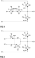
- FIG. 1 a semiconductor arrangement is schematically illustrated.
- the semiconductor arrangement of Figure 1 may include and may be operated in the way of an NPC (Neutral-Point Clamped) topology (i.e. a so-called NPC2 topology).
- Figure 1 is a circuit diagram of an exemplary three-level NPC2 topology.
- the semiconductor arrangement in Figure 1 includes a first supply node P1 which is configured to be operatively connected to a first electrical potential.
- the semiconductor arrangement further includes a second supply node N1 which is configured to be operatively connected to a second electrical potential.
- the first potential is positive with reference to the second potential.
- the first potential may be a positive potential DC+ and the second potential may be a negative potential DC-.
- the arrangement further includes a first controllable semiconductor element T1 and a second controllable semiconductor element T2.
- Each of the first controllable semiconductor element T1 and the second controllable semiconductor element T2 includes a control electrode G1, G2 and a controllable load path between a first load electrode (e.g., collector or drain electrode) and a second load electrode (e.g., emitter or source electrode).
- the load paths of the first controllable semiconductor element T1 and the second controllable semiconductor element T2 are coupled in series and between the first supply node P1 and the second supply node N1.
- the first controllable semiconductor element T1 i.e. the second load electrode of the first controllable semiconductor element T1
- the second controllable semiconductor element T2 i.e.
- the first load electrode of the second controllable semiconductor element T2 are connected with each other via a first common node forming an output node AC1.
- the first load electrode of the first controllable semiconductor element T1 is connected to the first supply node P 1
- the second load electrode of the second controllable semiconductor element T2 is connected to the second supply node N1.
- the arrangement further includes a third controllable semiconductor element T3 and a fourth controllable semiconductor element T4.
- Each of the third controllable semiconductor element T3 and the fourth controllable semiconductor element T4 includes a control electrode G3, G4 and a controllable load path between a first load electrode (e.g., collector or drain electrode) and a second load electrode (e.g., emitter or source electrode).
- the load paths of the third controllable semiconductor element T3 and the fourth controllable semiconductor element T4 are coupled in series and between the output node AC1 and a midpoint node M (often also referred to as neutral node).
- the third controllable semiconductor element T3 i.e.
- the second load electrode of the third controllable semiconductor element T3) and the fourth controllable semiconductor element T4 are connected with each other via a second common node, wherein the third controllable semiconductor element T3 is arranged between the second common node and the output node AC1, and the fourth controllable semiconductor element T4 is arranged between the second common node and the midpoint node M.
- Each of the controllable semiconductor elements T1, T2, T3, T4 may be implemented by means of a single component or by means of a plurality of identical controllable semiconductor subcomponents, each subcomponent having a control electrode and a controllable load path between a first load electrode and a second load electrode, the load paths being operatively connected in parallel between the nodes between which the respective controllable semiconductor element is connected.
- Each of the controllable semiconductor elements T1, T2, T3, T4 may include an intrinsic freewheeling element such as a body diode, which is electrically connected between the first load electrode and the second load electrode of the respective controllable semiconductor element T1, T2, T3, T4 (intrinsic freewheeling elements not specifically illustrated in Figure 1 ).
- the semiconductor arrangement further includes first, second, third and fourth freewheeling elements D1, D2, D3, D4.
- Each of the first, second, third, and fourth freewheeling elements D1, D2, D3, D4 includes a first electrode (e.g., anode) and a second electrode (e.g., cathode).
- Each of the first, second, third and fourth freewheeling elements D1, D2, D3, D4 may be connected in parallel to one of the controllable semiconductor elements T1, T2, T3, T4.
- the first freewheeling element D1 may be connected to the first supply node P1 with its second electrode and to the first common node (output node AC1) with its first electrode such that it is connected between the first supply node P1 and the output node AC1 and in parallel to the load path of the first controllable semiconductor element T1.
- the second freewheeling element D2 may be connected to the output node AC1 with its second electrode and to the second supply node N1 with its first electrode such that it is connected between the output node AC1 and the second supply node N1 and in parallel to the load path of the second controllable semiconductor element T2.
- the third freewheeling element D3 may be connected to the output node AC1 with its second electrode and to the second common node with its first electrode such that it is connected between the output node AC1 and the second common node and in parallel to the load path of the third controllable semiconductor element T3.
- the fourth freewheeling element D4 may be connected to the midpoint node M with its second electrode and to the second common node with its first electrode such that it is connected between the midpoint node M and the second common node and in parallel to the load path of the fourth controllable semiconductor element T4.
- Each of the controllable semiconductor elements T1, T2, T3, T4 may further be connected to a respective auxiliary emitter node HE1, HE2, HE3, HE4.
- the second load electrode of each controllable semiconductor element T1, T2, T3, T4 may be connected to a respective auxiliary emitter node HE1, HE2, HE3, HE4.
- the auxiliary emitter nodes HE1, HE2, HE3, HE4, however, are optional and may be omitted.
- Each of the controllable semiconductor elements T1, T2, T3, T4 may include a semiconductor switch.
- the individual semiconductor switches may include a transistor such as a MOSFET (Metal Oxide Semiconductor Field-Effect Transistor), IGBT (Insulated Gate Bipolar Transistor), JFET (Junction Field Effect Transistor), HEMT (High Electron Mobility Transistor), BIP (Bipolar Transistor), or any other kind of transistor, for example.
- MOSFET Metal Oxide Semiconductor Field-Effect Transistor
- IGBT Insulated Gate Bipolar Transistor
- JFET Joint Field Effect Transistor
- HEMT High Electron Mobility Transistor
- BIP Bipolar Transistor
- the semiconductor arrangement as illustrated in Figure 1 is configured to convert a DC voltage provided at an input P1, N1 into an AC voltage provided at the output node AC1.
- the AC voltage may be provided to, e.g., a load (not illustrated) that is coupled to the output node AC1 of the semiconductor arrangement.
- the load may be an inductive load, for example.
- the semiconductor arrangement instead of a single midpoint node M, comprises a first midpoint node M1 and a second midpoint node M2 which is separate and distinct from the first midpoint node M1.
- the first controllable semiconductor element T1, the second controllable semiconductor element T2, the first freewheeling element D1 and the second freewheeling element D2 are arranged similar to what has been described with respect to Figure 1 above.
- the fourth controllable semiconductor element T4 and the third freewheeling element D3, however, are coupled in series and between the output node AC1 and the first midpoint node M1.
- the fourth controllable semiconductor element T4 i.e. the second load electrode of the fourth controllable semiconductor element T4
- the third freewheeling element D3 i.e. the first electrode of the third freewheeling element D3
- the fourth controllable semiconductor element T4 is connected to the first midpoint node M1 with its first load electrode
- the third freewheeling element D3 is connected to the output node AC1 with its second electrode.
- the third controllable semiconductor element T3 and the fourth freewheeling element D4 are coupled in series and between the output node AC1 and the second midpoint node M2.
- the third controllable semiconductor element T3 i.e. the second load electrode of the third controllable semiconductor element T3
- the fourth freewheeling element D4 i.e. the first electrode of the fourth freewheeling element D4
- the third controllable semiconductor element T3 is connected to the output node AC1 with its first load electrode
- the fourth freewheeling element D4 is connected to the second midpoint node M2 with its second electrode.
- the third common node and the fourth common node may be separate and distinct from each other or may correspond to each other. This will be described in further detail below.
- first load electrode of the third controllable semiconductor element T3 and the second electrode of the fourth freewheeling element D4 may then be connected with each other via the fourth common node such that the third controllable semiconductor element T3 is connected to the output node AC1 with its second load electrode, and the fourth freewheeling element D4 is connected to the second midpoint node M2 with its first electrode.
- Such an arrangement may also be referred to as “common collector” arrangement.
- the principles described herein apply equally for "common emitter” and “common collector” arrangements.
- a first main commutation loop is indicated by means of the solid arrows
- a second main commutation loop is indicated by means of the dashed arrows, wherein the arrows indicate a current flow within the respective main commutation loop. That is, the first controllable semiconductor element T1 and the third freewheeling element D3 may be active at the same time while, e.g., the second controllable semiconductor element T2 and the fourth freewheeling element D4 are inactive.
- the second controllable semiconductor element T2 and the fourth freewheeling element D4 may be active while, e.g., the first controllable semiconductor element T1 and the third freewheeling element D3 are inactive.
- a third main commutation loop is indicated by means of the solid arrows
- a fourth main commutation loop is indicated by means of the dashed arrows in Figure 4 , wherein the arrows indicate a current flow within the respective main commutation loop. That is, the fourth controllable semiconductor element T4 and the second freewheeling element D2 may be active at the same time while, e.g., the third controllable semiconductor element T3 and the first freewheeling element D1 are inactive.
- the third controllable semiconductor element T3 and the first freewheeling element D1 may be active at the same time while, e.g., the fourth controllable semiconductor element T4 and the second freewheeling element D2 are inactive.
- the resulting output current (or reactive power for negative power factor, cos ⁇ ) is the same as illustrated in Figure 3B .
- Negative power factors may arise in a failure mode, while positive power factors are generally targeted in applications as a main operation mode (e.g., in solar applications). Therefore, for certain load cases, semiconductor arrangements may have to cover negative power factors as well.
- An example for such a load case may be a grid failure such as, e.g., a low voltage ride through.
- the main commutation loops as illustrated in Figure 4 usually have high stray inductances.
- the semiconductor arrangement of Figure 2 can be implemented in a single power semiconductor module arrangement 80.
- the power semiconductor module arrangement 80 comprises two separate substrates 102, 104. Those elements that are active at the same time are arranged together on one of the substrates 102, 104.
- any elements included in the first main commutation loop may be arranged on a first substrate 102
- any elements included in the second main commutation loop e.g., second controllable semiconductor element T2, second freewheeling element D2, third controllable semiconductor element T3, fourth freewheeling element D4
- the arrangement of the elements in Figure 5 is illustrated only very schematically.
- a substrate comprises a dielectric insulation layer and a metallization layer arranged on the dielectric insulation layer.
- the metallization layer usually is a structured layer.
- the metallization layer comprises recesses between different separate sections of the metallization layer. Different sections may be coupled to different potentials. Different semiconductor elements (semiconductor bodies) may be arranged on different sections of the metallization layer. Electrical connections between semiconductor elements and further sections of the first metallization layer may further be implemented by means of electrical connection elements such as, e.g., bonding wires or bonding ribbons. Different sections of the metallization layer as well as electrical connections, however, are not specifically illustrated in Figure 5 , as this is not required for understanding the general principle of the present disclosure.
- Figure 5 further illustrates very generally different terminals arranged on the respective substrates 102, 104 that form or are connected to the respective nodes as illustrated in Figure 3A . That is, terminals forming or connected to the first supply node P1, terminals forming or connected to the output node AC1, and terminals forming or connected to the first midpoint node M1 are arranged on the first substrate 102, while terminals forming or connected to the second supply node N1, terminals forming or connected to the output node AC1, and terminals forming or connected to the second midpoint node M2 are arranged on the second substrate 104. In this way, the main commutation loops are essentially separated. Terminals that form or are coupled to different nodes and potentials are generally arranged on different sections of the metallization layer. Such details, however, are omitted in Figure 5 for the sake of simplicity.
- Exemplary current flows in the semiconductor module arrangement of Figure 5 are illustrated in Figure 7 , wherein Figure 7A illustrates exemplary current flows for positive power factors cos ⁇ , and Figure 7B illustrates exemplary current flows for negative power factors cos ⁇ .
- Figure 7A illustrates exemplary current flows for positive power factors cos ⁇
- Figure 7B illustrates exemplary current flows for negative power factors cos ⁇ .
- the current flows are completely separated. That is, while the first main commutation loop is active, currents will flow solely on the first substrate 102 (indicated by solid arrows), and while the second main commutation loop is active, currents will flow solely on the second substrate 104 (indicated by dashed arrows). Only during failure mode (negative power factors ⁇ ), currents may flow on both substrates 102, 104 at the same time.
- any fast switching elements e.g., one or more semiconductor bodies forming the first controllable semiconductor element T1
- any slow switching elements e.g., one or more semiconductor bodies forming the fourth controllable semiconductor element T4
- any slow switching elements e.g., one or more semiconductor bodies forming the fourth controllable semiconductor element T4
- any slow switching elements e.g., one or more semiconductor bodies forming the fourth controllable semiconductor element T4
- any fast switching elements e.g., one or more semiconductor bodies forming the second controllable semiconductor element T2
- any slow switching elements e.g., one or more semiconductor bodies forming the third controllable semiconductor element T3
- any slow switching elements e.g., one or more semiconductor bodies forming the third controllable semiconductor element T3
- FIG. 6 This is schematically illustrated in Figure 6 .
- fast switching transistors and diodes such as SiC or GaN transistors and diodes, for example, are used to implement switches to allow for a fast switching of the semiconductor arrangement.
- fast switching semiconductor elements are usually comparatively expensive. Therefore, implementing each individual switch (semiconductor element) of a semiconductor arrangement as a fast switching element may be very costly. Some semiconductor elements (switches) are therefore usually implemented as slow switching devices. By implementing at least some of the switching elements as slow switching elements, the overall cost of a semiconductor module arrangement may be reduced.
- a fast switching element generally is a switching element that may perform a switching operation (e.g., from the on-state to an off-state or vice versa) at a certain speed.
- a threshold speed may be defined in this regard. If a switching element switches faster than the threshold speed, it may be defined as fast switching element. If a switching element switches slower than the threshold speed, it may be defined as slow switching element.
- a switching element having a turn-on time of ⁇ 100ns (nanoseconds) and a turn-off time of ⁇ 100ns may be seen as a fast switching device
- a switching element having a turn-on time of ⁇ 100ns (nanoseconds) and a turn-off time of ⁇ 100ns may be seen as a slow switching device.
- the components may be arranged on the different substrates 102, 104 in a similar way.
- the components on the first substrate 102 may be arranged symmetrically to the components on the second substrate 104.
- the arrangement of the components on the different substrate 102, 104 may result in an essentially similar performance for the two subsystems (for positive and negative sine half-wave of the output current).
- the layouts on the separate substrates 102, 104 may result in an essentially symmetric electrical performance of the two subsystems. That is, the current flows on the separate substrates 102, 104 may be very similar, but not necessarily exactly symmetric.
- a first electrical connection 51 may be provided between the output potential AC1 on the first substrate 102 and the output potential AC1 on the second substrate 104.
- the first electrical connection 51 may include one or more electrical connection elements such as, e.g., bonding wires, bonding ribbons, or connection rails, for example.
- a second electrical connection 52 may be provided between an auxiliary potential on the first substrate 102 and an auxiliary potential on the second substrate 104.
- an auxiliary emitter HE4 of the fourth controllable semiconductor element T4 arranged on the first substrate 102, and an auxiliary emitter HE3 of the third controllable semiconductor element T3 on the second substrate 104 may be electrically coupled by means of the second electrical connection 52.
- the second electrical connection 52 may include one or more electrical connection elements such as, e.g., bonding wires, bonding ribbons, or connection rails, for example.
- the first midpoint node M1 on the first substrate 102, and the second midpoint node M2 on the second substrate 104 may be separated from each other on the different substrates 102, 104. That is, no electrical connection may be provided to electrically couple the first and second midpoint nodes M1, M2 to each other.
- the fourth controllable semiconductor element T4 is generally sufficiently protected against reverse currents. The same applies for the third controllable semiconductor element T3, during forward recovery of the fourth freewheeling element D4.
- electrically connecting the first midpoint node M1 and the second midpoint node M2 to each other is generally not required.
- the third and fourth controllable semiconductor elements T3, T4 are semiconductor devices that are able to conduct a current in reverse direction.
- semiconductor devices include, e.g., RC-IGBTs or MOSFETS.
- the third and fourth freewheeling elements D3, D4 take over a DC-link voltage during reverse recovery, there is no need for implementing a commutation robustness, for example.
- the first and second midpoint nodes M1, M2 do not need to be connected to each other, there is free space on the substrates 102, 104 which may be used to implement interconnections between the output nodes AC1 on the different substrates 102, 104, for example. Establishing a low-inductive connection between the output node AC1 on the first substrate 102, and the output node AC1 on the second substrate 104 allows a sound operation of the semiconductor arrangement also during failure mode (negative power factors cos ⁇ ).
- each subgroup is arranged on a different one of two substrates 102, 104 and comprises the elements that are included in a respective one of the main commutation loops of the semiconductor arrangement for positive power factors cos ⁇ . That is, during normal operation of the semiconductor arrangement, the elements arranged on the first substrate 102 are active at the same time, resulting in currents flowing on the first substrate 102 while no current is flowing on the second substrate 104, and the elements arranged on the second substrate 104 are active at the same time, resulting in currents flowing on the second substrate 104 while no current is flowing on the first substrate 102.
- the separation of the current flows on separate substrates 102, 104 is achieved by providing two separate midpoint nodes M1, M2 that are not directly connected to each other.
- failure mode negative power factors cos ⁇
- currents may flow on both substrates 102, 104 at the same time. For this reason, certain electrical connections may be provided between the different substrates 102, 104.
- first controllable semiconductor element T1, the first freewheeling element D1, the third controllable semiconductor element T3, and the fourth freewheeling element D4 on the first substrate 102, and the second controllable semiconductor element T2, the second freewheeling element D2, the fourth controllable semiconductor element T4, and the third freewheeling element D3 on the second substrate 104 (not specifically illustrated in the figures).
- failure mode of the semiconductor arrangement (negative power factors cos ⁇ )
- the elements arranged on the first substrate 102 are active at the same time, resulting in currents flowing on the first substrate 102 while no current is flowing on the second substrate 104
- the elements arranged on the second substrate 104 are active at the same time, resulting in currents flowing on the second substrate 104 while no current is flowing on the first substrate 102.
- currents may then flow on both substrates 102, 104 at the same time.
- the mode referred to as failure mode herein may be considered normal operation mode instead and vice versa. The principles that have been discussed above similar apply for such an alternative arrangement.
- Figure 9 schematically illustrates a top view of a power semiconductor module arrangement 80 comprising a first substrate 102 and a second substrate 104.
- a metallization layer comprising a plurality of different sections 112 1 , 112 2 , 112 3 , 112 4 is arranged on a dielectric insulation layer of the first substrate 102, and a metallization layer comprising a plurality of different sections 114 1 , 114 2 , 114 3 , 114 4 is arranged on a dielectric insulation layer of the second substrate 104.
- a first section 112i of the metallization layer of the first substrate 102 may be electrically coupled to the first supply node P1.
- One or more semiconductor bodies forming the first controllable semiconductor element T1 as well as one or more semiconductor bodies forming the first freewheeling element D1 are arranged on the first section 112i of the metallization layer of the first substrate 102.
- Each of the one or more semiconductor bodies forming the first controllable semiconductor element T1 and each of the one or more semiconductor bodies forming the first freewheeling element D1 may be electrically coupled to the first section 112i of the metallization layer of the first substrate 102 by means of an electrically conducting connection layer.
- Each of the one or more semiconductor bodies forming the first controllable semiconductor element T1 and each of the one or more semiconductor bodies forming the first freewheeling element D1 may be electrically coupled to a second section 112 2 of the metallization layer of the first substrate 102 by means of one or more electrical connections (e.g., bonding wires or ribbons).
- the second section 112 2 of the metallization layer of the first substrate 102 may be electrically coupled to the output node AC1.
- One or more semiconductor bodies forming the third freewheeling element D3 may be arranged on the second section 112 2 .
- One or more semiconductor bodies forming the fourth controllable semiconductor element T4 are arranged on a third section 112 3 of the metallization layer of the first substrate 102.
- Each of the one or more semiconductor bodies forming the fourth controllable semiconductor element T4 may be electrically coupled to the third section 112 3 by means of an electrically conductive connection layer.
- the third section 112 3 may be electrically coupled to the first midpoint node M1.
- Each of the one or more semiconductor bodies forming the third freewheeling element D3, and each of the one or more semiconductor bodies forming the fourth controllable semiconductor element T4 may be electrically coupled to a fourth section 112 4 of the metallization layer of the first substrate 102 by means of one or more electrical connections (e.g., bonding wires or ribbons).
- One or more semiconductor bodies forming the second controllable semiconductor element T2 and one or more semiconductor bodies forming the second freewheeling element D2 may be arranged on a first section 114i of the metallization layer of the second substrate 104.
- Each of the one or more semiconductor bodies forming the second controllable semiconductor element T2 and each of the one or more semiconductor bodies forming the second freewheeling element D2 may be electrically coupled to the first section 114i by means of an electrically conducting connection layer, for example.
- Each of the one or more semiconductor bodies forming the second controllable semiconductor element T2 and each of the one or more semiconductor bodies forming the second freewheeling element D2 may be electrically coupled to a second section 114 2 of the metallization layer of the second substrate 104, e.g., by means of one or more electrical connections (e.g., bonding wires or ribbons).
- the first section 114i may be electrically coupled to the output node AC1
- the second section 114 2 may be electrically coupled to the second supply node N1.
- One or more semiconductor bodies forming the fourth freewheeling element D4 are arranged on a third section 114 3 of the metallization layer of the second substrate 104.
- the third section 114 3 may be electrically coupled to the second midpoint node M2.
- One or more semiconductor bodies forming the third controllable semiconductor element T3 are arranged on and electrically coupled to (e.g., by means of an electrically conducting connection layer ) the first section 114i of the metallization layer of the second substrate 104.
- Each of the one or more semiconductor bodies forming the third controllable semiconductor element T3, and each of the one or more semiconductor bodies forming the fourth freewheeling element D4 may be electrically coupled to a fourth section 114 4 of the metallization layer of the second substrate 104, e.g., by means of one or more electrical connections (e.g., bonding wires or ribbons).
- the second section 112 2 of the metallization layer of the first substrate 102 and the first section 114i of the metallization layer of the second substrate 104 may be electrically coupled to each other, e.g., by means of one or more electrical connections (e.g., bonding wires or ribbons).
- the fourth section 112 4 of the metallization layer of the first substrate 102 may form the third common node
- the fourth section 114 4 of the metallization layer of the second substrate 104 may form the fourth common node.
- the third common node and the fourth common node may be electrically connected to each other.
- the fourth section 112 4 of the metallization layer of the first substrate 102 and the fourth section 114 4 of the metallization layer of the second substrate 104 may be electrically coupled to each other, e.g., by means of one or more electrical connections (e.g., bonding wires or ribbons).
- the one or more electrical connections between the fourth section 112 4 of the metallization layer of the first substrate 102 and the fourth section 114 4 of the metallization layer of the second substrate 104 as well as the one or more electrical connections between the second section 112 2 of the metallization layer of the first substrate 102 and the first section 114i of the metallization layer of the second substrate 104 provide a low inductive connection between the first substrate 102 and the second substrate 104.
- a protection diode may be arranged anti-parallel to the third controllable semiconductor element T3, and a further protection diode may be arranged anti-parallel to the fourth controllable semiconductor element T4.
- the voltage class of such protection diode may be chosen to be the same or higher than the voltage class of the third and fourth controllable semiconductor element T3, T4, respectively.
- a low current rating may be chosen for the protection diodes, as the protection diodes only need to carry a reverse current for a comparably short period during reverse recovery of the third freewheeling element D3 or the fourth freewheeling element D4, respectively.
Landscapes
- Engineering & Computer Science (AREA)
- Power Engineering (AREA)
- Power Conversion In General (AREA)
Priority Applications (1)
| Application Number | Priority Date | Filing Date | Title |
|---|---|---|---|
| EP23159870.7A EP4425780A1 (fr) | 2023-03-03 | 2023-03-03 | Agencement de semi-conducteur et agencement de module semi-conducteur |
Applications Claiming Priority (1)
| Application Number | Priority Date | Filing Date | Title |
|---|---|---|---|
| EP23159870.7A EP4425780A1 (fr) | 2023-03-03 | 2023-03-03 | Agencement de semi-conducteur et agencement de module semi-conducteur |
Publications (1)
| Publication Number | Publication Date |
|---|---|
| EP4425780A1 true EP4425780A1 (fr) | 2024-09-04 |
Family
ID=85462142
Family Applications (1)
| Application Number | Title | Priority Date | Filing Date |
|---|---|---|---|
| EP23159870.7A Withdrawn EP4425780A1 (fr) | 2023-03-03 | 2023-03-03 | Agencement de semi-conducteur et agencement de module semi-conducteur |
Country Status (1)
| Country | Link |
|---|---|
| EP (1) | EP4425780A1 (fr) |
Citations (5)
| Publication number | Priority date | Publication date | Assignee | Title |
|---|---|---|---|---|
| DE102013104081B3 (de) * | 2013-04-23 | 2014-05-15 | Semikron Elektronik Gmbh & Co. Kg | 3-Level-Stromrichterhalbbrücke |
| US9577627B2 (en) * | 2014-12-18 | 2017-02-21 | Mitsubishi Electric Corporation | Semiconductor device |
| WO2017202749A1 (fr) * | 2016-05-23 | 2017-11-30 | Danfoss Silicon Power Gmbh | Agencement de convertisseur |
| EP3442108B1 (fr) * | 2016-04-08 | 2020-12-30 | Toshiba Mitsubishi-Electric Industrial Systems Corporation | Convertisseur de secteur multiniveaux |
| US20220319976A1 (en) * | 2019-05-26 | 2022-10-06 | Danfoss Silicon Power Gmbh | Three-level power module |
-
2023
- 2023-03-03 EP EP23159870.7A patent/EP4425780A1/fr not_active Withdrawn
Patent Citations (5)
| Publication number | Priority date | Publication date | Assignee | Title |
|---|---|---|---|---|
| DE102013104081B3 (de) * | 2013-04-23 | 2014-05-15 | Semikron Elektronik Gmbh & Co. Kg | 3-Level-Stromrichterhalbbrücke |
| US9577627B2 (en) * | 2014-12-18 | 2017-02-21 | Mitsubishi Electric Corporation | Semiconductor device |
| EP3442108B1 (fr) * | 2016-04-08 | 2020-12-30 | Toshiba Mitsubishi-Electric Industrial Systems Corporation | Convertisseur de secteur multiniveaux |
| WO2017202749A1 (fr) * | 2016-05-23 | 2017-11-30 | Danfoss Silicon Power Gmbh | Agencement de convertisseur |
| US20220319976A1 (en) * | 2019-05-26 | 2022-10-06 | Danfoss Silicon Power Gmbh | Three-level power module |
Non-Patent Citations (2)
| Title |
|---|
| GURPINAR EMRE ET AL: "Single-Phase T-Type Inverter Performance Benchmark Using Si IGBTs, SiC MOSFETs, and GaN HEMTs", IEEE TRANSACTIONS ON POWER ELECTRONICS, INSTITUTE OF ELECTRICAL AND ELECTRONICS ENGINEERS, USA, vol. 31, no. 10, 1 October 2016 (2016-10-01), pages 7148 - 7160, XP011610941, ISSN: 0885-8993, [retrieved on 20160520], DOI: 10.1109/TPEL.2015.2506400 * |
| ZHAO XINGCHEN ET AL: "Design of Ultracompact Gate Driver Integrated With Current Sensor and Commutation Path for a 211-kW Three-Level SiC Aircraft Propulsion Inverter", IEEE JOURNAL OF EMERGING AND SELECTED TOPICS IN POWER ELECTRONICS, IEEE, PISCATAWAY, NJ, USA, vol. 11, no. 4, 21 February 2023 (2023-02-21), pages 4077 - 4094, XP011945981, ISSN: 2168-6777, [retrieved on 20230222], DOI: 10.1109/JESTPE.2023.3247378 * |
Similar Documents
| Publication | Publication Date | Title |
|---|---|---|
| CN102449898B (zh) | 功率转换装置 | |
| US10123443B2 (en) | Semiconductor device | |
| JP4594477B2 (ja) | 電力半導体モジュール | |
| CN103444068B (zh) | 具有能反向导通的功率半导体开关的模块化多重变流器 | |
| CN104011861B (zh) | 集成电路的单块单元并且尤其是单块转换单元 | |
| US6657874B2 (en) | Semiconductor converter circuit and circuit module | |
| JP7337711B2 (ja) | 半導体装置 | |
| CN102347702A (zh) | 高效半桥直流到交流转换器 | |
| US20200119658A1 (en) | Bridge circuit for inverter or rectifier | |
| JP6934823B2 (ja) | 3レベルiタイプインバータおよび半導体モジュール | |
| US7180762B2 (en) | Cascoded rectifier | |
| CN102024814B (zh) | Mos-栅功率半导体器件 | |
| US20250220938A1 (en) | Semiconductor device and power conversion device | |
| EP3396839B1 (fr) | Agencement semi-conducteur avec des éléments à semi-conducteur commandables | |
| EP3057232A1 (fr) | Dispositif de coupe-circuit | |
| EP4425780A1 (fr) | Agencement de semi-conducteur et agencement de module semi-conducteur | |
| CN114079446A (zh) | 开关装置及用于制造开关装置的方法 | |
| US12334427B2 (en) | Semiconductor device | |
| US20220239234A1 (en) | Power conversion device | |
| JP2015201947A (ja) | パワー半導体デバイス | |
| JP2015222777A (ja) | 半導体装置およびそれを用いた電力変換装置 | |
| WO2023112570A1 (fr) | Dispositif semiconducteur et dispositif de conversion de puissance | |
| CN115995987B (zh) | 一种基于串联拓扑结构的功率模块 | |
| CN119852277B (zh) | 混合功率模块、多相全桥混合模块、电力转换装置和车辆 | |
| US11398418B2 (en) | Semiconductor module |
Legal Events
| Date | Code | Title | Description |
|---|---|---|---|
| PUAI | Public reference made under article 153(3) epc to a published international application that has entered the european phase |
Free format text: ORIGINAL CODE: 0009012 |
|
| STAA | Information on the status of an ep patent application or granted ep patent |
Free format text: STATUS: EXAMINATION IS IN PROGRESS |
|
| 17P | Request for examination filed |
Effective date: 20231220 |
|
| AK | Designated contracting states |
Kind code of ref document: A1 Designated state(s): AL AT BE BG CH CY CZ DE DK EE ES FI FR GB GR HR HU IE IS IT LI LT LU LV MC ME MK MT NL NO PL PT RO RS SE SI SK SM TR |
|
| STAA | Information on the status of an ep patent application or granted ep patent |
Free format text: STATUS: THE APPLICATION IS DEEMED TO BE WITHDRAWN |
|
| 18D | Application deemed to be withdrawn |
Effective date: 20241029 |