EP3447801A1 - Élément d'imagerie à semi-conducteur, procédé de commande et dispositif électronique - Google Patents
Élément d'imagerie à semi-conducteur, procédé de commande et dispositif électronique Download PDFInfo
- Publication number
- EP3447801A1 EP3447801A1 EP17785819.8A EP17785819A EP3447801A1 EP 3447801 A1 EP3447801 A1 EP 3447801A1 EP 17785819 A EP17785819 A EP 17785819A EP 3447801 A1 EP3447801 A1 EP 3447801A1
- Authority
- EP
- European Patent Office
- Prior art keywords
- electric charge
- pixel
- multiplication region
- photoelectric conversion
- conversion unit
- Prior art date
- Legal status (The legal status is an assumption and is not a legal conclusion. Google has not performed a legal analysis and makes no representation as to the accuracy of the status listed.)
- Withdrawn
Links
Images












Classifications
-
- H—ELECTRICITY
- H04—ELECTRIC COMMUNICATION TECHNIQUE
- H04N—PICTORIAL COMMUNICATION, e.g. TELEVISION
- H04N25/00—Circuitry of solid-state image sensors [SSIS]; Control thereof
- H04N25/70—SSIS architectures; Circuits associated therewith
- H04N25/76—Addressed sensors, e.g. MOS or CMOS sensors
- H04N25/77—Pixel circuitry, e.g. memories, A/D converters, pixel amplifiers, shared circuits or shared components
- H04N25/778—Pixel circuitry, e.g. memories, A/D converters, pixel amplifiers, shared circuits or shared components comprising amplifiers shared between a plurality of pixels, i.e. at least one part of the amplifier must be on the sensor array itself
-
- H—ELECTRICITY
- H04—ELECTRIC COMMUNICATION TECHNIQUE
- H04N—PICTORIAL COMMUNICATION, e.g. TELEVISION
- H04N25/00—Circuitry of solid-state image sensors [SSIS]; Control thereof
- H04N25/70—SSIS architectures; Circuits associated therewith
- H04N25/71—Charge-coupled device [CCD] sensors; Charge-transfer registers specially adapted for CCD sensors
- H04N25/711—Time delay and integration [TDI] registers; TDI shift registers
-
- H—ELECTRICITY
- H04—ELECTRIC COMMUNICATION TECHNIQUE
- H04N—PICTORIAL COMMUNICATION, e.g. TELEVISION
- H04N25/00—Circuitry of solid-state image sensors [SSIS]; Control thereof
- H04N25/70—SSIS architectures; Circuits associated therewith
- H04N25/76—Addressed sensors, e.g. MOS or CMOS sensors
- H04N25/77—Pixel circuitry, e.g. memories, A/D converters, pixel amplifiers, shared circuits or shared components
- H04N25/771—Pixel circuitry, e.g. memories, A/D converters, pixel amplifiers, shared circuits or shared components comprising storage means other than floating diffusion
-
- H—ELECTRICITY
- H04—ELECTRIC COMMUNICATION TECHNIQUE
- H04N—PICTORIAL COMMUNICATION, e.g. TELEVISION
- H04N25/00—Circuitry of solid-state image sensors [SSIS]; Control thereof
- H04N25/70—SSIS architectures; Circuits associated therewith
- H04N25/79—Arrangements of circuitry being divided between different or multiple substrates, chips or circuit boards, e.g. stacked image sensors
-
- H—ELECTRICITY
- H10—SEMICONDUCTOR DEVICES; ELECTRIC SOLID-STATE DEVICES NOT OTHERWISE PROVIDED FOR
- H10F—INORGANIC SEMICONDUCTOR DEVICES SENSITIVE TO INFRARED RADIATION, LIGHT, ELECTROMAGNETIC RADIATION OF SHORTER WAVELENGTH OR CORPUSCULAR RADIATION
- H10F30/00—Individual radiation-sensitive semiconductor devices in which radiation controls the flow of current through the devices, e.g. photodetectors
- H10F30/20—Individual radiation-sensitive semiconductor devices in which radiation controls the flow of current through the devices, e.g. photodetectors the devices having potential barriers, e.g. phototransistors
-
- H—ELECTRICITY
- H10—SEMICONDUCTOR DEVICES; ELECTRIC SOLID-STATE DEVICES NOT OTHERWISE PROVIDED FOR
- H10F—INORGANIC SEMICONDUCTOR DEVICES SENSITIVE TO INFRARED RADIATION, LIGHT, ELECTROMAGNETIC RADIATION OF SHORTER WAVELENGTH OR CORPUSCULAR RADIATION
- H10F30/00—Individual radiation-sensitive semiconductor devices in which radiation controls the flow of current through the devices, e.g. photodetectors
- H10F30/20—Individual radiation-sensitive semiconductor devices in which radiation controls the flow of current through the devices, e.g. photodetectors the devices having potential barriers, e.g. phototransistors
- H10F30/21—Individual radiation-sensitive semiconductor devices in which radiation controls the flow of current through the devices, e.g. photodetectors the devices having potential barriers, e.g. phototransistors the devices being sensitive to infrared, visible or ultraviolet radiation
- H10F30/22—Individual radiation-sensitive semiconductor devices in which radiation controls the flow of current through the devices, e.g. photodetectors the devices having potential barriers, e.g. phototransistors the devices being sensitive to infrared, visible or ultraviolet radiation the devices having only one potential barrier, e.g. photodiodes
- H10F30/225—Individual radiation-sensitive semiconductor devices in which radiation controls the flow of current through the devices, e.g. photodetectors the devices having potential barriers, e.g. phototransistors the devices being sensitive to infrared, visible or ultraviolet radiation the devices having only one potential barrier, e.g. photodiodes the potential barrier working in avalanche mode, e.g. avalanche photodiodes
-
- H—ELECTRICITY
- H10—SEMICONDUCTOR DEVICES; ELECTRIC SOLID-STATE DEVICES NOT OTHERWISE PROVIDED FOR
- H10F—INORGANIC SEMICONDUCTOR DEVICES SENSITIVE TO INFRARED RADIATION, LIGHT, ELECTROMAGNETIC RADIATION OF SHORTER WAVELENGTH OR CORPUSCULAR RADIATION
- H10F39/00—Integrated devices, or assemblies of multiple devices, comprising at least one element covered by group H10F30/00, e.g. radiation detectors comprising photodiode arrays
- H10F39/10—Integrated devices
- H10F39/12—Image sensors
-
- H—ELECTRICITY
- H10—SEMICONDUCTOR DEVICES; ELECTRIC SOLID-STATE DEVICES NOT OTHERWISE PROVIDED FOR
- H10F—INORGANIC SEMICONDUCTOR DEVICES SENSITIVE TO INFRARED RADIATION, LIGHT, ELECTROMAGNETIC RADIATION OF SHORTER WAVELENGTH OR CORPUSCULAR RADIATION
- H10F39/00—Integrated devices, or assemblies of multiple devices, comprising at least one element covered by group H10F30/00, e.g. radiation detectors comprising photodiode arrays
- H10F39/10—Integrated devices
- H10F39/12—Image sensors
- H10F39/18—Complementary metal-oxide-semiconductor [CMOS] image sensors; Photodiode array image sensors
- H10F39/182—Colour image sensors
- H10F39/1825—Multicolour image sensors having stacked structure, e.g. NPN, NPNPN or multiple quantum well [MQW] structures
-
- H—ELECTRICITY
- H10—SEMICONDUCTOR DEVICES; ELECTRIC SOLID-STATE DEVICES NOT OTHERWISE PROVIDED FOR
- H10F—INORGANIC SEMICONDUCTOR DEVICES SENSITIVE TO INFRARED RADIATION, LIGHT, ELECTROMAGNETIC RADIATION OF SHORTER WAVELENGTH OR CORPUSCULAR RADIATION
- H10F39/00—Integrated devices, or assemblies of multiple devices, comprising at least one element covered by group H10F30/00, e.g. radiation detectors comprising photodiode arrays
- H10F39/80—Constructional details of image sensors
- H10F39/803—Pixels having integrated switching, control, storage or amplification elements
-
- H—ELECTRICITY
- H10—SEMICONDUCTOR DEVICES; ELECTRIC SOLID-STATE DEVICES NOT OTHERWISE PROVIDED FOR
- H10F—INORGANIC SEMICONDUCTOR DEVICES SENSITIVE TO INFRARED RADIATION, LIGHT, ELECTROMAGNETIC RADIATION OF SHORTER WAVELENGTH OR CORPUSCULAR RADIATION
- H10F39/00—Integrated devices, or assemblies of multiple devices, comprising at least one element covered by group H10F30/00, e.g. radiation detectors comprising photodiode arrays
- H10F39/80—Constructional details of image sensors
- H10F39/805—Coatings
- H10F39/8057—Optical shielding
Definitions
- the present disclosure relates to a solid-state image sensor, a driving method, and an electronic apparatus, and in particular, to a solid-state image sensor, driving method, and electronic apparatus, capable of achieving reduction in pixel size and sensitivity improvement.
- a solid-state image sensor such as charge-coupled device (CCD) or complementary metal-oxide-semiconductor (CMOS) image sensor has been used.
- the solid-state image sensor has a pixel in which a photodiode (PD) that performs photoelectric conversion and a plurality of transistors are combined, and an image is constructed on the basis of pixel signals that are output from a plurality of pixels arranged on an image plane on which an image of a photographic subject is formed.
- PD photodiode
- a technique capable of preventing the decrease in saturated electric charge amount, sensitivity, or the like and of improving random noise, random telegraph signal (RTS) noise, or the like by separating a PD and a transistor in the depth direction has been developed (e.g., refer to Patent Literature 1).
- an imaging device including a multiplier sensor for multiplying electrons due to impact ionization by an electric field in order to further improve the sensitivity has been developed (e.g., refer to Patent Literature 2).
- CMOS image sensors As a silicon-based multiplication sensor, an avalanche photodiode (APD), single-photon avalanche diode (SPAD), or the like is widely used, but its pixel structure and circuit configuration are completely novel, unlike CMOS image sensors in related art. For this reason, such a multiplication sensor is difficult to apply to the CMOS image sensors in related art because the compatibility of the techniques is low.
- CMOS sensors having a multiplication region called electron multiplier CMOS (EMCMOS) have been recently performed, but the necessity to additionally provide a multiplication region makes achievement of reduction in pixel size difficult.
- EMCMOS electron multiplier CMOS
- the present disclosure is made in view of such a situation, and is intended to make it possible to achieve reduction in pixel size and sensitivity improvement.
- a solid-state image sensor includes: a photoelectric conversion unit configured to convert light into electric charge by photoelectric conversion and to store the electric charge; a read-out unit configured to read out the electric charge stored in the photoelectric conversion unit; a multiplication region configured to store temporarily and multiply the electric charge read out through the read-out unit; and a transfer unit configured to transfer the electric charge stored in the multiplication region to a conversion unit configured to convert the electric charge into a pixel signal.
- a method of driving a solid-state image sensor including a photoelectric conversion unit configured to convert light into electric charge by photoelectric conversion and to store the electric charge; a read-out unit configured to read out the electric charge stored in the photoelectric conversion unit, a multiplication region configured to store temporarily and multiply the electric charge read out through the read-out unit, and a transfer unit configured to transfer the electric charge stored in the multiplication region to a conversion unit configured to convert the electric charge into a pixel signal, the method including a step of generating an intense electric field region in the multiplication region to multiply electric charge by an avalanche effect in transferring the electric charge from the multiplication region to the conversion unit through the transfer unit.
- an electronic apparatus includes a solid-state image sensor including a photoelectric conversion unit configured to convert light into electric charge by photoelectric conversion and to store the electric charge, a read-out unit configured to read out the electric charge stored in the photoelectric conversion unit, a multiplication region configured to store temporarily and multiply the electric charge read out through the read-out unit, and a transfer unit configured to transfer the electric charge stored in the multiplication region to a conversion unit configured to convert the electric charge into a pixel signal.
- the photoelectric conversion unit allows electric charge converted from light by photoelectric conversion to be stored
- the read-out unit allows the electric charge stored in the photoelectric conversion unit to be read out
- the multiplication region allows the electric charge read out through the read-out unit to be stored temporarily and multiplied
- the transfer unit allows the electric charge stored in the multiplication region to be transferred to the conversion unit configured to convert electric charge into a pixel signal.
- FIG. 1 is a block diagram illustrating a configuration example of an embodiment of an image sensor to which the present technology is applied.
- an image sensor 11 includes a pixel region 12, a vertical drive circuit 13, a column signal processing circuit 14, a horizontal drive circuit 15, an output circuit 16, and a control circuit 17.
- the pixel region 12 is a light receiving surface that receives light collected by an optical system (not illustrated).
- a plurality of pixels 21 are arranged in a matrix form, and each of the pixels 21 is connected to the vertical drive circuit 13 row by row through a horizontal signal line 22 and is connected to the column signal processing circuit 14 column by column through a vertical signal line 23.
- Each of the plurality of pixels 21 output a pixel signal at a level corresponding to the quantity of light to be received, and an image of a photographic subject to be formed on the pixel region 12 is constructed from these pixel signals.
- the vertical drive circuit 13 supplies a drive signal, which is used to drive (transfer, select, reset, or the like) each pixel 21 sequentially for each row of the plurality of pixels 21 arranged in the pixel region 12, to the pixel 21 through the horizontal signal line 22.
- the column signal processing circuit 14 performs the correlated double sampling (CDS) processing on pixel signals that are output from the plurality of pixels 21 through the vertical signal line 23, thereby performing AD conversion on the pixel signals and removing reset noise.
- CDS correlated double sampling
- the horizontal drive circuit 15 supplies a drive signal, which is used to cause the column signal processing circuit 14 to output a pixel signal to a data output signal line 24, to the column signal processing circuit 14 sequentially for each column of the plurality of pixels 21 arranged in the pixel region 12.
- the output circuit 16 amplifies the pixel signal supplied from the column signal processing circuit 14 through the data output signal line 24 at the timing in accordance with the drive signal of the horizontal drive circuit 15 and outputs it to a signal processing circuit of the following stage.
- the control circuit 17 generates and supplies, in one example, a clock signal in accordance with the driving cycle of each block of the image sensor 11, thereby controlling the driving of these respective blocks.
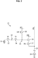
- FIG. 2 is a circuit diagram illustrating a configuration example of the pixel 21.
- the pixel 21 includes a PD 31, a first transfer transistor 32, a multiplication region 33, a second transfer transistor 34, a floating diffusion (FD) portion 35, an amplification transistor 36, a selection transistor 37, and a reset transistor 38, and is connected to a constant current source 39 through the vertical signal line 23.
- a PD 31 a first transfer transistor 32, a multiplication region 33, a second transfer transistor 34, a floating diffusion (FD) portion 35, an amplification transistor 36, a selection transistor 37, and a reset transistor 38, and is connected to a constant current source 39 through the vertical signal line 23.
- FD floating diffusion
- the PD 31 is a photoelectric conversion unit that converts incident light into electric charge by photoelectric conversion and stores it, and has an anode grounded and a cathode connected to the first transfer transistor 32.
- the first transfer transistor 32 is driven in accordance with a transfer signal VG supplied from the vertical drive circuit 13, and when the first transfer transistor 32 is turned on, the electric charge stored in the PD 31 is transferred to the multiplication region 33.
- the multiplication region 33 is a floating diffusion region that has predetermined storage capacity and is provided between the first transfer transistor 32 and the second transfer transistor 34, and temporarily stores the electric charge transferred from the PD 31.
- the multiplication region 33 is capable of multiplying electrons by producing an intense electric field region therein to cause avalanche effect (i.e., a phenomenon in which free electrons collide with molecules in an intense electric field, releasing additional electrons which accelerate and collide with other molecules in an electric field, so the number of electrons increases with increasing speed).
- the second transfer transistor 34 is driven in accordance with a transfer signal TG supplied from the vertical drive circuit 13, and when the second transfer transistor 34 is turned on, the electric charge stored in the multiplication region 33 is transferred to the FD portion 35.
- the FD portion 35 is a floating diffusion region that has predetermined storage capacity and is connected to the gate electrode of the amplification transistor 36, and temporarily stores the electric charge transferred through the multiplication region 33.
- the amplification transistor 36 outputs a pixel signal at a level (i.e., the potential of the FD portion 35) corresponding to the electric charge stored in the FD portion 35 to the vertical signal line 23 through the selection transistor 37.
- a level i.e., the potential of the FD portion 35
- the configuration in which the FD portion 35 is connected to the gate electrode of the amplification transistor 36 allows the FD portion 35 and the amplification transistor 36 to amplify the electric charge generated in the PD 31 and to function as a conversion unit that converts it into a pixel signal at the level corresponding to the electric charge.
- the selection transistor 37 is driven in accordance with a selection signal SEL supplied from the vertical drive circuit 13, and when the selection transistor 37 is turned on, the pixel signal output from the amplification transistor 36 is ready to be outputted to the vertical signal line 23.
- the reset transistor 38 is driven in accordance with a reset signal RST supplied from the vertical drive circuit 13, and when the reset transistor 38 is turned on, the electric charge stored in the FD portion 35 is discharged to a variable power source VFC, and the FD portion 35 is reset.
- the variable power source VFC can change the voltage so that the reset potential of the multiplication region 33 is different from that of the FD portion 35, as described with reference to FIGS. 4 to 7 .
- the pixel 21 configured as described above makes it possible for the electric charge (electrons) generated in the PD 31 to be multiplied by reading out it through the multiplication region 33.
- FIG. 3 is a cross-sectional view illustrating a first configuration example of the pixel 21.
- the PD 31 is formed on the back surface side (the lower side in FIG. 2 ) of a semiconductor substrate 41, and the PD 31 is irradiated with light from the back surface side of the semiconductor substrate 41. Then, a color filter 42 and an on-chip lens 43 are stacked on the back surface side of the semiconductor substrate 41.
- the color filter 42 transmits light of a color received by the pixel 21, and the on-chip lens 43 collects light for each pixel 21.
- the first transfer transistor 32, the multiplication region 33, the second transfer transistor 34, and the FD portion 35 are arranged on the front surface side of the semiconductor substrate 41.
- the first transfer transistor 32 has a gate electrode 44 provided to be defined by digging a trench from the front surface of the semiconductor substrate 41 to the vicinity of the side surface of the PD 31 at a portion adjacent to the multiplication region 33.
- the first transfer transistor 32 has a so-called vertical transistor structure, and the electric charge generated in the PD 31 is read out to the front surface of the semiconductor substrate 41 and is transferred to the multiplication region 33.
- the multiplication region 33 is arranged on the front surface side of the semiconductor substrate 41 so that it is stacked on the PD 31 arranged on the back surface side of the semiconductor substrate 41, and stores electric charge to be read out through the first transfer transistor 32.
- a high voltage is applied to the second transfer transistor 34.
- an avalanche effect is created by producing an intense electric field region inside the multiplication region 33, thereby multiplying electrons.
- application of an optional negative bias to the first transfer transistor 32 makes it possible to enhance the multiplication effect of electrons.
- the second transfer transistor 34 has a gate electrode 45 provided to be stacked on the front surface of the semiconductor substrate 41 between the multiplication region 33 and the FD portion 35. Then, the second transfer transistor 34 transfers the electric charge, which is read out from the PD 31 and is stored in the multiplication region 33, to the FD portion 35.
- the FD portion 35 stores the electric charge transferred from the multiplication region 33 through the second transfer transistor 34 and is connected to the gate electrode of the amplification transistor 36 as described above with reference to FIG. 2 .
- the pixel 21 is provided with a light blocking portion 46 capable of blocking light to prevent the light incident on other pixels 21 adjacent thereto from entering the pixel 21 so that the light blocking portion 46 is embedded from the back surface side of the semiconductor substrate 41 to a predetermined depth in such a way as to enclose the periphery of the PD 31.
- the pixel 21 configured as described above has, in one example, the structure in which the PD 31, the multiplication region 33, and the PD 31 are provided in such a way to be stacked vertically above one another, thereby achieving the size reduction.
- the pixel 21 it is possible to multiply the electric charge (electrons) generated in the PD 31 by reading out it through the multiplication region 33. This makes it possible for the pixel 21 to obtain a pixel signal with high sensitivity, in one example, even at low illuminance.
- the image sensor 11 including the pixel 21 can employ a structure similar to that of the CMOS image sensor in related art with respect to the photoelectric conversion characteristics in the PD 31 or the electric-charge transfer conversion characteristics from the PD 31. Furthermore, in the image sensor 11, the number of transistors necessary for the pixel 21 can be made smaller than that of the APD in related art, and so it is possible to achieve size reduction of the pixel 21, thereby being configured with the higher integration and being provided with the multiplication function.
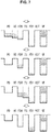
- FIGS. 4 and 5 illustrate an electric potential of the PD 31 (PD), an electric potential of the transfer signal of the first transfer transistor 32 (VG), an electric potential of the multiplication region 33 (FD0), an electric potential of the transfer signal of the second transfer transistor 34 (TG), an electric potential of the FD portion 35 (FD1), an electric potential of the reset signal of the reset transistor 38 (RST), and an electric potential of the variable power source VFC (VF).
- the electric potential of the variable power source is set to, in one example, 3 V, and the first transfer transistor 32, the second transfer transistor 34, and the reset transistor 38 are driven to be turned on. This causes the electric charge remaining in the PD 31 to be discharged through the reset transistor 38, the FD portion 35, the second transfer transistor 34, the multiplication region 33, and the first transfer transistor 32, then the PD 31 is reset.
- the first transfer transistor 32 is driven to be turned off. This causes the PD 31 to start to store the electric charge generated by photoelectric conversion.
- the electric potential of the variable power source VFC is changed to, in one example, 11 V. This causes the multiplication region 33 to be reset to 11 V through the reset transistor 38, the FD portion 35, and the second transfer transistor 34.
- the second transfer transistor 34 is driven to be turned off, and then the electric potential of the variable power source VFC is changed to, in one example, 12 V. This causes the FD portion 35 to be reset to 12 V through the reset transistor 38.
- the reset transistor 38 is driven to be turned off, and then the reset operation is terminated.
- the first transfer transistor 32 is driven to be turned on. This causes the storage of electric charge in the PD 31 to be terminated and causes the transfer of electric charge from the PD 31 to the multiplication region 33 to be performed while occurring the multiplication. In this event, an intense electric field region is caused to be produced in the multiplication region 33 to multiply the electric charge by the avalanche effect.
- the first transfer transistor 32 is driven to be turned off. This causes the transfer of electric charge from the PD 31 to the multiplication region 33 to be terminated.
- a negative bias is applied to the first transfer transistor 32 and the second transfer transistor 34. This causes the electric potential of the multiplication region 33 to be stepped down.
- the second transfer transistor 34 is driven to be turned on. This causes the transfer of electric charge from the multiplication region 33 to the FD portion 35 to be performed normally.
- the second transfer transistor 34 is driven to be turned off. This causes the transfer of electric charge from the multiplication region 33 to the FD portion 35 to be terminated. Then, a pixel signal at a level corresponding to the electric charge stored in the FD portion 35 is output from the amplification transistor 36 in FIG. 2 .
- Such a first driving method makes it possible for the pixel 21 to multiply the electric charge generated in the PD 31 when the electric charge is read out to the multiplication region 33.
- the electric potential of the variable power source is set to, in one example, 3 V, and the first transfer transistor 32, the second transfer transistor 34, and the reset transistor 38 are driven to be turned on. This causes the electric charge remaining in the PD 31 to be discharged through the reset transistor 38, the FD portion 35, the second transfer transistor 34, the multiplication region 33, and the first transfer transistor 32, and then the PD 31 is reset.
- the first transfer transistor 32 is driven to be turned off. This causes the PD 31 to start to store the electric charge generated by photoelectric conversion.
- the electric potential of the variable power source VFC is changed to, in one example, 4 V. This causes the multiplication region 33 to be reset to 4 V through the reset transistor 38, the FD portion 35, and the second transfer transistor 34.
- the second transfer transistor 34 is driven to be turned off, and then the electric potential of the variable power source VFC is changed to, in one example, 12 V. This causes the FD portion 35 to be reset to 12 V through the reset transistor 38.
- the reset transistor 38 is driven to be turned off, and then the reset operation is terminated.
- the first transfer transistor 32 is driven to be turned on. This causes the storage of electric charge in the PD 31 to be terminated and causes the transfer of electric charge from the PD 31 to the multiplication region 33 to be performed normally.
- the first transfer transistor 32 is driven to be turned off. This causes the transfer of electric charge from the PD 31 to the multiplication region 33 to be terminated.
- the second transfer transistor 34 is driven to be turned on. This causes the transfer of electric charge from the multiplication region 33 to the FD portion 35 to be performed while occurring the multiplication. In this event, an intense electric field region is caused to be produced in the multiplication region 33 to multiply the electric charge by the avalanche effect.
- the second transfer transistor 34 is driven to be turned off. This causes the transfer of electric charge from the multiplication region 33 to the FD portion 35 to be terminated. Then, a pixel signal at a level corresponding to the electric charge stored in the FD portion 35 is output from the amplification transistor 36 in FIG. 2 .
- Such a second driving method makes it possible for the pixel 21 to multiply the electric charge generated in the PD 31 and read out to the multiplication region 33 when the electric charge is transferred to the FD portion 35. Furthermore, employing the second driving method makes it possible to separate the portion for reading out the electric charge from the PD 31 and the portion for multiplying the electric charge, and these portions can be designed as independent device structure.
- impurities are ion-implanted into the semiconductor substrate 41 to form the PD 31 in the vicinity of the front surface of the semiconductor substrate 41.
- crystal growth is performed on the semiconductor substrate 41 to form an epitaxial layer.
- impurities are ion-implanted into the epitaxial layer of the semiconductor substrate 41 to form the multiplication region 33. Furthermore, a trench is defined in the semiconductor substrate 41 by digging it to the vicinity of the side surface of the PD 31 at a portion adjacent to the multiplication region 33 and then a conductor is deposited onto the trench to form the gate electrode 44, and so the first transfer transistor 32 is provided. In this event, the gate electrode 45 is formed to be stacked on the semiconductor substrate 41, and so the second transfer transistor 34 is provided.
- the fourth process as shown in the fourth stage from the top in FIG. 8 , impurities are ion-implanted into the epitaxial layer of the semiconductor substrate 41 to form the FD portion 35. Then, the pixel 21 is manufactured through a process of thinning the back surface side of the semiconductor substrate 41, stacking the color filter 42 and the on-chip lens 43 thereon, and providing a wiring layer (not illustrated) or the like.
- the pixel 21 it is possible for the pixel 21 to have a structure in which the PD 31 and the multiplication region 33 are stacked on each other by forming the PD 31 in the semiconductor substrate 41, and forming the epitaxial layer, then forming the multiplication region 33 in the epitaxial layer.
- impurities are ion-implanted into the semiconductor substrate 41 to form the PD 31 in the deep portion of the semiconductor substrate 41.
- impurities are ion-implanted into the semiconductor substrate 41 to form the multiplication region 33 in the vicinity of the front surface of the semiconductor substrate 41.
- the gate electrode 44 and the gate electrode 45 are formed to provide the first transfer transistor 32 and the second transfer transistor 34, respectively, and then the FD portion 35 is formed. Then, the pixel 21 is manufactured through a process of thinning the back surface side of the semiconductor substrate 41, stacking the color filter 42 and the on-chip lens 43 thereon, and providing a wiring layer (not illustrated) or the like.
- the pixel 21 it is possible for the pixel 21 to have a structure in which the PD 31 and the multiplication region 33 are stacked on each other by separately forming the PD 31 and the multiplication region 33 by separating the depth direction when impurities are ion-implanted into the same semiconductor substrate 41.
- the PD 31 is formed in a first semiconductor substrate 41-1, and the multiplication region 33 is formed in a second semiconductor substrate 41-2.
- the first semiconductor substrate 41-1 and the second semiconductor substrate 41-2 are bonded to each other.
- the gate electrode 44 and the gate electrode 45 are formed to provide the first transfer transistor 32 and the second transfer transistor 34, respectively, and then the FD portion 35 is formed. Then, the pixel 21 is manufactured through a process of thinning the back surface side of the semiconductor substrate 41, stacking the color filter 42 and the on-chip lens 43 thereon, and providing a wiring layer (not illustrated) or the like.
- the PD 31 and the multiplication region 33 are formed in the first semiconductor substrate 41-1 and the second semiconductor substrate 41-2, respectively.
- the semiconductor substrate 41 is formed by bonding first semiconductor substrate 41-1 and the second semiconductor substrate 41-2 to each other. Accordingly, the pixel 21 can have a structure in which the PD 31 and the multiplication region 33 are stacked on each other.
- the pixel 21 having the structure in which the PD 31 and the multiplication region 33 are stacked on each other may be manufactured by employing any one of the first to third manufacturing methods as described above. Moreover, it is possible to employ methods other than the above-described manufacturing methods as long as the PD 31 and the multiplication region 33 can be stacked on each other.
- FIG. 11 is a cross-sectional view illustrating a second configuration example of the pixel 21. Moreover, in a pixel 21A illustrated in FIG. 11 , the components common to those of the pixel 21 in FIG. 3 are denoted by the same reference numerals, and a detailed description thereof will be omitted.
- the pixel 21A has a structure common to that of the pixel 21 in FIG. 3 in that the PD 31, the first transfer transistor 32, the multiplication region 33, the FD portion 35, and the light blocking portion 46 are provided in the semiconductor substrate 41, and the color filter 42 and the on-chip lens 43 are stacked on the back surface of the semiconductor substrate 41.
- the structure of a second transfer transistor 34A is different from that of the second transfer transistor 34 of the pixel 21 in FIG. 3 .
- the second transfer transistor 34A has a gate electrode 45A formed to be embedded in the semiconductor substrate 41 in such a way that it extends from the front surface side of the semiconductor substrate 41 to the PD 31.
- the second transfer transistor 34A has a so-called vertical transistor structure, which is similar to the first transfer transistor 32.
- the pixel 21A can read out electric charge directly from the PD 31 to the FD portion 35 through the second transfer transistor 34A when the second transfer transistor 34A is driven to be turned on in a state where electric charge is stored in the PD 31.
- the pixel 21A can read out the electric charge stored in the PD 31 by two driving methods, that is, the driving method of reading out electric charge from the PD 31 through the first transfer transistor 32 and the driving method of reading out electric charge from the PD 31 through the second transfer transistor 34A.
- the driving method of reading out the electric charge directly from the PD 31 to the FD portion 35 through the second transfer transistor 34A is used.
- a pixel signal in which the electric charge is not multiplied is read out.
- a driving method of reading out the electric charge from the PD 31 to the multiplication region 33 through the first transfer transistor 32, amplifying it, and then transferring the electric charge to the FD portion 35 through the transfer transistor 34A is used.
- a pixel signal in which the electric charge is multiplied is read out.
- the electric charge of the PD 31 has been read out through the first transfer transistor 32, and so no electric charge is read out from the PD 31 through the second transfer transistor 34A.
- the pixel 21A configured as described above is capable of switching the driving methods of reading out the electric charge from the PD 31, thereby capturing an image with appropriate exposure depending on, in one example, the brightness of a photographic subject.
- FIG. 12 is a cross-sectional view illustrating a third configuration example of the pixel 21. Moreover, in a pixel 21B illustrated in FIG. 12 , the components common to those of the pixel 21 in FIG. 3 are denoted by the same reference numerals, and a detailed description thereof will be omitted.
- the pixel 21B has a structure common to that of the pixel 21 in FIG. 3 in that the PD 31, the first transfer transistor 32, the multiplication region 33, the FD portion 35, and the light blocking portion 46 are provided in the semiconductor substrate 41, and the color filter 42 and the on-chip lens 43 are stacked on the back surface of the semiconductor substrate 41.
- the structure of a second transfer transistor 34B is different from the structure of the second transfer transistor 34 of the pixel 21 in FIG. 3 .
- a gate electrode 45B included in the second transfer transistor 34B is larger in size than the gate electrode 45 in FIG. 3 and is formed to cover the multiplication region 33 in a wider region.
- the transfer signal TG applied to the gate electrode 45B it is possible to enhance the electric field generated in the multiplication region 33 by the transfer signal TG applied to the gate electrode 45B.
- the pixel 21B configured as described above enhances the electric field generated in the multiplication region 33, and so it is possible to assist multiplication of electric charge, thereby further multiplying the electric charge.
- FIG. 13 is a cross-sectional view illustrating a fourth configuration example of the pixel 21. Moreover, in a pixel 21C illustrated in FIG. 13 , the components common to those of the pixel 21 in FIG. 3 are denoted by the same reference numerals, and a detailed description thereof will be omitted.
- the pixel 21C has a structure common to that of the pixel 21 in FIG. 3 in that the PD 31, the multiplication region 33, the second transfer transistor 34, the FD portion 35, and the light blocking portion 46 are provided in the semiconductor substrate 41, and the color filter 42 and the on-chip lens 43 are stacked on the back surface of the semiconductor substrate 41.
- the structure of a first transfer transistor 32C is different from that of the first transfer transistor 32 of the pixel 21 in FIG. 3 .
- a gate electrode 44C included in the first transfer transistor 32C has a length larger than that of the gate electrode 44 in FIG. 3 and is formed deep into the semiconductor substrate 41, so that more portions of the gate electrode 44C are adjacent to the PD 31.
- the pixel 21C configured as described above is capable of assisting the transfer of electric charge from the PD 31 to the multiplication region 33, thereby transferring the electric charge more satisfactorily and reading out reliably the electric charge stored in the PD 31.
- FIG. 14 is a cross-sectional view illustrating a fifth configuration example of the pixel 21. Moreover, in a pixel 21D illustrated in FIG. 14 , the components common to those of the pixel 21 in FIG. 3 are denoted by the same reference numerals, and a detailed description thereof will be omitted.
- the pixel 21D has a structure common to that of the pixel 21 in FIG. 3 in that the PD 31, the multiplication region 33, the FD portion 35, and the light blocking portion 46 are provided in the semiconductor substrate 41, and the color filter 42 and the on-chip lens 43 are stacked on the back surface of the semiconductor substrate 41.
- the structures of a first transfer transistor 32D and a second transfer transistor 34D are different from those of the first transfer transistor 32 and the second transfer transistor 34 of the pixel 21 in FIG. 3 , respectively.
- a gate electrode 44D included in the first transfer transistor 32D has a length larger than that of the gate electrode 45 in FIG. 3 , which is similar to the gate electrode 45C in FIG. 13 , and is formed so that more portions of the gate electrode 44D are adjacent to the PD 31.
- a gate electrode 45D included in the second transfer transistor 34D is larger in size than the gate electrode 45 in FIG. 3 , which is similar to the gate electrode 45B in FIG. 12 , and is formed to cover the multiplication region 33 in a wider region.
- the pixel 21D configured as described above is capable of further multiplying electric charge, which is similar to the pixel 21B in FIG. 12 , and is capable of reliably reading out the electric charge stored in the PD 31, which is similar to the pixel 21C in FIG. 13 .
- FIG. 15 is a cross-sectional view illustrating a sixth configuration example of the pixel 21. Moreover, in a pixel 21E illustrated in FIG. 15 , the components common to those of the pixel 21 in FIG. 3 are denoted by the same reference numerals, and a detailed description thereof will be omitted.
- the pixel 21E has a structure common to the pixel 21 in FIG. 3 in that the PD 31, the first transfer transistor 32, the multiplication region 33, the second transfer transistor 34, and the FD portion 35 are provided in the semiconductor substrate 41, and the color filter 42 and the on-chip lens 43 are stacked on the back surface of the semiconductor substrate 41.
- the structure of a light blocking portion 46E is different from that of the light blocking portion 46 of the pixel 21 in FIG. 3 .
- the light blocking portion 46E included in the pixel 21E has a length larger than that of the light blocking portion 46 in FIG. 3 , and is formed to have substantially the same depth as the depth from the back surface of the semiconductor substrate 41 to the region where the PD 31 is formed.
- the light blocking portion 46E is formed to have substantially the same depth as the thickness of the first semiconductor substrate 41-1.
- the light blocking portion 46E reliably blocks light incident on each of the adjacent pixels 21, and so, in one example, it is possible to prevent light from entering the multiplication region 33 from other adjacent pixels 21. This makes it possible for the pixel 21E to prevent occurrence of color mixture (parasitic light sensitivity: PLS) or the like in the multiplication region 33.
- PLS parsitic light sensitivity
- FIG. 16 is a cross-sectional view illustrating a seventh configuration example of the pixel 21. Moreover, in a pixel 21F illustrated in FIG. 16 , the components common to those of the pixel 21 in FIG. 3 are denoted by the same reference numerals, and a detailed description thereof will be omitted.
- the pixel 21F has a structure common to the pixel 21 in FIG. 3 in that the PD 31, the first transfer transistor 32, the multiplication region 33, the second transfer transistor 34, the FD portion 35, and the light blocking portion 46 are provided in the semiconductor substrate 41, and the color filter 42 and the on-chip lens 43 are stacked on the back surface of the semiconductor substrate 41.
- the pixel 21F is different in configuration from the pixel 21 in FIG. 3 in that it includes a light blocking film 47.
- the pixel 21F has the light blocking film 47 equipped with light blocking characteristics, which is provided between the multiplication region 33 and the layer provided with the PD 31.
- Such a light blocking structure makes it possible for the pixel 21F to prevent light emitting from the back surface side of the semiconductor substrate 41 from reaching the multiplication region 33 through the semiconductor substrate 41.
- the light blocking film 47 is capable of reliably blocking the light transmitted through the semiconductor substrate 41 from reaching the multiplication region 33, thereby preventing, in one example, occurrence of color mixture (parasitic light sensitivity: PLS) or the like in the multiplication region 33.
- the light blocking portion 46E included in the pixel 21E in FIG. 15 and the light blocking film 47 included in the pixel 21F in FIG. 16 may be combined, and both the light blocking portion 46E and the light blocking film 47 can prevent occurrence of color mixture or the like in the multiplication region 33 more reliably.
- FIG. 17 is a cross-sectional view illustrating an eighth configuration example of the pixel 21. Moreover, in a pixel 21G illustrated in FIG. 17 , the components common to those of the pixel 21 in FIG. 3 are denoted by the same reference numerals, and a detailed description thereof will be omitted.
- the pixel 21G has a structure common to that of the pixel 21 in FIG. 3 in that the PD 31, the first transfer transistor 32, the multiplication region 33, the second transfer transistor 34, the FD portion 35, and the light blocking portion 46 are provided in the semiconductor substrate 41, and the color filter 42 and the on-chip lens 43 are stacked on the back surface of the semiconductor substrate 41.
- the pixel 21G is different from the pixel 21 in FIG. 3 in that it includes multiplication gate electrodes 48-1 to 48-3.
- the pixel 21G has a configuration in which multiplication gate electrodes 48-1 to 48-3 are stacked on the front surface of the multiplication region 33 in the semiconductor substrate 41.
- the multiplication gate electrodes 48-1 to 48-3 are arranged to be aligned with one another from the first transfer transistor 32 toward the second transfer transistor 34.
- the pixel 21G formed as described above enhances the electric field generated in the multiplication region 33, and so it is possible to assist multiplication of electric charge, thereby further multiplying electric charge.
- the number of the multiplication gate electrodes 48 illustrated in FIG. 17 , the bias voltage to be applied to the multiplication gate electrode 48, or the like is optionally specified depending on the extent to which electrons are multiplied in the multiplication region 33.
- FIG. 18 is a cross-sectional view illustrating a ninth configuration example of the pixel 21. Moreover, in a pixel 21H illustrated in FIG. 18 , the components common to those of the pixel 21 in FIG. 3 are denoted by the same reference numerals, and a detailed description thereof will be omitted.
- the pixel 21H has a structure common to the pixel 21 in FIG. 3 in that the PD 31, the first transfer transistor 32, the multiplication region 33, the second transfer transistor 34, the FD portion 35, and the light blocking portion 46 are provided in the semiconductor substrate 41, and the color filter 42 and the on-chip lens 43 are stacked on the back surface of the semiconductor substrate 41.
- the pixel 21H is different from the pixel 21 in FIG. 3 in that it includes multiplication gate electrodes 49-1 to 49-3.
- the pixel 21H has a configuration in which the multiplication gate electrodes 49-1 to 49-3 are embedded in the semiconductor substrate 41 so that they penetrate the multiplication region 33 from the front surface of the multiplication region 33 in the semiconductor substrate 41.
- the multiplication gate electrodes 49-1 to 49-3 are arranged to be aligned with one another from the first transfer transistor 32 toward the second transfer transistor 34.
- the pixel 21H formed as described above enhances the electric field generated in the multiplication region 33 and so it is possible to assist the multiplication of electric charge, thereby further multiplying electric charge.
- the number of the multiplication gate electrodes 49 illustrated in FIG. 18 , the bias voltage to be applied to the multiplication gate electrode 49, or the like is optionally specified depending on the extent to which electrons are multiplied in the multiplication region 33.
- the multiplication gate electrode 48 illustrated in FIG. 17 and the multiplication gate electrode 49 illustrated in FIG. 18 may be arranged in such a way that they are combined.
- FIG. 19 is a cross-sectional view illustrating a tenth configuration example of the pixel 21. Moreover, in a pixel 21J illustrated in FIG. 19 , the components common to those of the pixel 21 in FIG. 3 are denoted by the same reference numerals, and a detailed description thereof will be omitted.
- the pixel 21J has a structure common to the pixel 21 in FIG. 3 in that the PD 31, the first transfer transistor 32, the multiplication region 33, the second transfer transistor 34, the FD portion 35, and the light blocking portion 46 are provided in the semiconductor substrate 41.
- the pixel 21J has a different structure from the pixel 21 in FIG. 3 in that an on-chip lens 43 is stacked on the back surface of the semiconductor substrate 41 through an organic film 50 and a color filter 42J.
- a color filter that transmits yellow or cyan light is used as the color filter 42J, and an organic film that has sensitivity to light of a specific wavelength component, for example, green light is used as the organic film 50.
- the color filter 42J that transmits yellow light among light transmitted through the color filter 42J, the green light is photoelectrically converted by the organic film 50 and the red light transmitted through the organic film 50 is photoelectrically converted by the PD 31.
- the green light is photoelectrically converted by the organic film 50 and the blue light is photoelectrically converted by the PD 31.
- the PD 31 performs the photoelectric conversion in the pixel 21 in FIG. 3 , whereas both the organic film 50 and the PD 31 perform the photoelectric conversion in the pixel 21J.
- the pixel 21J configured as described above is capable of multiplying electrons generated by the red and blue light photoelectrically converted by the PD 31 in the multiplication region 33, thereby enhancing the sensitivity of red and blue to a level comparable to the sensitivity of green that is photoelectrically converted in the organic film 50.
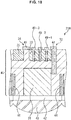
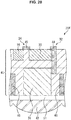
- FIG. 20 is a cross-sectional view illustrating an eleventh configuration example of the pixel 21. Moreover, in a pixel 21K illustrated in FIG. 20 , the components common to those of the pixel 21 in FIG. 3 are denoted by the same reference numerals, and a detailed description thereof will be omitted.
- the pixel 21K has a structure common to the pixel 21 in FIG. 3 in that the PD 31, the first transfer transistor 32, the multiplication region 33, the second transfer transistor 34, the FD portion 35, and the light blocking portion 46 are provided in the semiconductor substrate 41.
- the pixel 21K has a different structure from the pixel 21 in FIG. 3 in that the on-chip lens 43 is stacked on the back surface of the semiconductor substrate 41 through an inorganic film 51.
- the pixel 21K it is possible to photoelectrically convert a specific wavelength component by the inorganic film 51 and to photoelectrically convert other wavelength components by the PD 31.
- the use of an inorganic film having sensitivity to infrared light as the inorganic film 51 makes it possible for the pixel 21K to have a structure in which, among light incident on the pixel 21K, infrared light is photoelectrically converted by the inorganic film 51, but light of other wavelength components are photoelectrically converted by the PD 31.
- the inorganic film 51 as an infrared light cut filter.
- only the PD 31 performs the photoelectric conversion in the pixel 21 in FIG. 3 , whereas the photoelectric conversion is performed in both the organic film 50 and the PD 31 in the pixel 21K.
- the pixel 21K configured as described above is capable of reading out the electric charge, which is generated by photoelectric conversion of components other than a specific wavelength component by the PD 31, through the multiplication region 33.
- FIG. 21 is a cross-sectional view illustrating a twelfth configuration example of the pixel 21. Moreover, in a pixel 21L illustrated in FIG. 21 , the components common to those of the pixel 21 in FIG. 3 are denoted by the same reference numerals, and a detailed description thereof will be omitted.
- the pixel 21L has a structure common to the pixel 21 in FIG. 3 in that the PD 31, the first transfer transistor 32, the multiplication region 33, the second transfer transistor 34, the FD portion 35, and the light blocking portion 46 are provided in the semiconductor substrate 41.
- the pixel 21L has a different structure from the pixel 21 in FIG. 3 in that the on-chip lens 43 is stacked on the back surface of the semiconductor substrate 41 through an organic film 52, an organic film 53, and the organic film 50.
- an organic film that has sensitivity to blue light is used as the organic film 52, and an organic film that has sensitivity red light is used as the organic film 52.
- an organic film that has sensitivity to green light is used as the organic film 50.
- blue, red, and green light are photoelectrically converted by the organic film 52, the organic film 53, and the organic film 50, respectively, and the infrared light transmitted through the organic film 52, the organic film 53, and the organic film 50 is photoelectrically converted by the PD 31.
- the pixel 21L configured as described above is capable of achieving high sensitivity characteristics for all of blue, red, green, and infrared light.
- FIG. 22 is a cross-sectional view illustrating a thirteenth configuration example of the pixel 21. Moreover, in a pixel 21M illustrated in FIG. 22 , the components common to those of the pixel 21 in FIG. 3 are denoted by the same reference numerals, and a detailed description thereof will be omitted.
- the pixel 21 in FIG. 3 has the arrangement configuration in which the PD 31 and the multiplication region 33 are provided in a stacked configuration
- the pixel 21M has an arrangement configuration in which the PD 31 and the multiplication region 33 are provided in the same layer without being stacked as illustrated in FIG. 22 , which is different from the pixel 21 in FIG. 3 .
- the pixel 21M has a configuration in which the PD 31 and the multiplication region 33 are arranged to be aligned in the same layer of the semiconductor substrate 41, and a gate electrode 44M of a first transfer transistor 32M is stacked on the front surface of the semiconductor substrate 41 between the PD 31 and the multiplication region 33.
- a light blocking film 54 is stacked on a region other than the region where the PD 31 is provided on the back surface of the semiconductor substrate 41 so that the incidence of light to other components than the PD 31 is blocked.
- the pixel 21M configured as described above is capable of multiplying the electric charge generated in the PD 31 by reading out it through the multiplication region 33, which is similar to the pixel 21 having the configuration in which the PD 31 and the multiplication region 33 are stacked on each other. This makes it possible for the pixel 21M to obtain a pixel signal with high sensitivity, in one example, even at low illuminance.
- the image sensor 11 including the pixel 21M can employ a structure similar to that of the CMOS image sensor in related art with respect to the photoelectric conversion characteristics in the PD 31 or the electric-charge transfer conversion characteristics from the PD 31. Furthermore, in the image sensor 11, the number of transistors necessary for the pixel 21 can be made smaller than that of the APD in related art, and so it is possible to achieve size reduction of the pixel 21M, thereby being configured with the higher integration and being provided with the multiplication function.
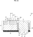
- FIG. 23 is a cross-sectional view illustrating a fourteenth configuration example of the pixel 21. Moreover, in a pixel 21N illustrated in FIG. 23 , the components common to those of the pixel 21M in FIG. 22 are denoted by the same reference numerals, and a detailed description thereof will be omitted.
- the pixel 21N has an arrangement configuration in which the PD 31 and the multiplication region 33 are provided in the same layer without being stacked, which is similar to the pixel 21M in FIG. 22 .
- the pixel 21N is different in configuration from the pixel 21M in FIG. 22 in that it includes the multiplication gate electrodes 48-1 to 48-3.
- the pixel 21N uses the multiplication gate electrodes 48-1 to 48-3 to enhance the electric field generated in the multiplication region 33, and so it is possible to assist the multiplication of electric charge, thereby further multiplying electric charge, which is similar to the pixel 21G in FIG. 17 .
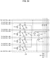
- FIG. 24 is a circuit diagram illustrating a fifteenth configuration example of the pixel 21. Moreover, in a pixel 21P illustrated in FIG. 24 , the components common to those of the pixel 21 in FIG. 2 are denoted by the same reference numerals, and a detailed description thereof will be omitted.
- the pixel 21P has a so-called 4-pixel sharing structure in which four PDs 31a to 31d share a pixel circuit including the FD portion 35, the amplification transistor 36, the selection transistor 37, and the reset transistor 38.
- the electric charge can be amplified in transferring the electric charge from multiplication regions 33a to 33d to the FD portion 35, and the output of the high-potential FD portion 35 can be input to the amplification transistor 36 with no change.
- the amplification transistor 36 is necessary to receive a high voltage as an input, and the use of a high voltage compatible transistor is necessary to have, in one example, an area larger than that of a low voltage compatible transistor.
- the pixel 21P having the 4-pixel sharing structure reduce the number of the amplification transistors 36, thereby achieving high integration.
- FIG. 25 is a circuit diagram illustrating a sixteenth configuration example of the pixel 21. Moreover, in a pixel 21Q illustrated in FIG. 25 , the components common to those of the pixel 21 in FIG. 2 are denoted by the same reference numerals, and a detailed description thereof will be omitted.
- the pixel 21Q has a so-called 8-pixel sharing structure in which eight PDs 31a to 31h share a pixel circuit including the FD portion 35, the amplification transistor 36, the selection transistor 37, and the reset transistor 38.
- the pixel 21Q having the 8-pixel sharing structure reduces the number of the amplification transistors 36, thereby achieving further high integration, as compared to the pixel 21P having the 4-pixel sharing structure in FIG. 24 .
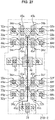
- FIG. 26 illustrates a planar layout example of the pixel 21Q having the 8-pixel sharing structure, in one example, in the arrangement configuration in which the PD 31 and the multiplication region 33 are not stacked as illustrated in FIG. 22 .
- FIG. 27 illustrates a planar layout example of the pixel 21Q having the 8-pixel sharing structure, in one example, in the arrangement configuration in which the PD 31 and the multiplication region 33 are stacked as illustrated in FIG. 3 .
- FIG. 28 illustrates a layout of the multiplication region 33 and the second transfer transistor 34 as viewed in planar view.
- an intense electric field of the order that may cause an increase of electrons due to the avalanche effect that is, an electric field of about 5.5E+5 [V/cm] at the maximum occurs near the edge of the gate electrode 45 indicated by a broken line in FIG. 28 .
- FIG. 29 shows the impact ionization probability (avalanche probability) for various semiconductor materials, where the horizontal axis represents the electric field [10 5 V/cm] and the vertical axis represents the impact ionization probability [cm -1 ].
- a e 1.34 ⁇ 10
- a h 1.44 ⁇ 10
- B e -1.05 ⁇ 10 6 V/cm
- B h -1.85 ⁇ 10 6 V/cm
- FIG. 30 the horizontal axis represents electric field, and the vertical axis represents gains in which the lengths to be the intense electric field region are set to 1 ⁇ m, 500 nm, and 100 nm on the basis of the electric charge with electrons (e) and holes (h).
- the generation of an appropriate intense electric field in the multiplication region 33 makes it possible to multiply the electric charge in transferring electric charge from the multiplication region 33 to the FD portion 35 by using the second transfer transistor 34 even if the structure similar to that of the CMOS image sensor in related art is employed.
- the image sensor 11 as described above is applicable to, in one example, various kinds of electronic apparatuses, such as an image capture system including a digital still camera, a digital video camera, and the like, a mobile telephone equipped with an imaging function, or other devices equipped with an imaging function.
- an image capture system including a digital still camera, a digital video camera, and the like
- a mobile telephone equipped with an imaging function or other devices equipped with an imaging function.
- FIG. 31 is a block diagram illustrating a configuration example of an image capture device installed in an electronic apparatus.
- the image capture device 101 includes an optical system 102, an image sensor 103, a signal processing circuit 104, a monitor 105, and a memory 106, and is able to capture still images and moving images.
- the optical system 102 includes one or more lenses, and guides image light (incident light) from a photographic subject to the image sensor 103 to form an image on a light receiving face (sensor unit) of the image sensor 103.
- the image sensor 11 described above is used as the image sensor 103.
- the image sensor 103 electrons are stored for a fixed period of time depending on an image formed on the light receiving face through the optical system 102. Then a signal corresponding to the electrons stored in the image sensor 103 is supplied to the signal processing circuit 104.
- the signal processing circuit 104 performs various signal processes on pixel signals output from the image sensor 103.
- An image (image data) obtained by the signal processing circuit 104 performing a signal process is supplied to the monitor 105 so to be displayed, or supplied to the memory 106 so as to be stored (recorded).
- the image capture device 101 configured as described above uses the above-described image sensor 11, thereby, in one example, achieving sensitivity improvement and capturing an image with higher image quality.
- FIG. 32 is a diagram illustrating a usage example of using the above-described image sensor 11 (image sensor).
- the above-described image sensor can be, in one example, used in various cases of sensing light such as visible light, infrared light, ultraviolet light, and X-ray as described below.
- present technology may also be configured as below.
Landscapes
- Engineering & Computer Science (AREA)
- Multimedia (AREA)
- Signal Processing (AREA)
- Solid State Image Pick-Up Elements (AREA)
- Transforming Light Signals Into Electric Signals (AREA)
Applications Claiming Priority (2)
| Application Number | Priority Date | Filing Date | Title |
|---|---|---|---|
| JP2016086551 | 2016-04-22 | ||
| PCT/JP2017/014452 WO2017183477A1 (fr) | 2016-04-22 | 2017-04-07 | Élément d'imagerie à semi-conducteur, procédé de commande et dispositif électronique |
Publications (2)
| Publication Number | Publication Date |
|---|---|
| EP3447801A1 true EP3447801A1 (fr) | 2019-02-27 |
| EP3447801A4 EP3447801A4 (fr) | 2020-03-25 |
Family
ID=60116912
Family Applications (1)
| Application Number | Title | Priority Date | Filing Date |
|---|---|---|---|
| EP17785819.8A Withdrawn EP3447801A4 (fr) | 2016-04-22 | 2017-04-07 | Élément d'imagerie à semi-conducteur, procédé de commande et dispositif électronique |
Country Status (6)
| Country | Link |
|---|---|
| US (2) | US10560652B2 (fr) |
| EP (1) | EP3447801A4 (fr) |
| JP (1) | JP7001967B2 (fr) |
| CN (1) | CN107851655A (fr) |
| DE (1) | DE112017002137T5 (fr) |
| WO (1) | WO2017183477A1 (fr) |
Cited By (2)
| Publication number | Priority date | Publication date | Assignee | Title |
|---|---|---|---|---|
| US12317623B2 (en) | 2019-12-02 | 2025-05-27 | Sony Semiconductor Solutions Corporation | Imaging apparatus, manufacturing method thereof, and electronic equipment |
| US12471402B2 (en) | 2019-12-03 | 2025-11-11 | Sony Semiconductor Solutions Corporation | Imaging apparatus, manufacturing method thereof, and electronic equipment |
Families Citing this family (19)
| Publication number | Priority date | Publication date | Assignee | Title |
|---|---|---|---|---|
| CN106791463B (zh) * | 2016-11-30 | 2019-08-20 | 上海集成电路研发中心有限公司 | 一种全局快门cmos像素单元及图像采集方法 |
| JP2019126013A (ja) * | 2018-01-19 | 2019-07-25 | ソニーセミコンダクタソリューションズ株式会社 | 固体撮像素子 |
| KR102506885B1 (ko) * | 2018-02-27 | 2023-03-06 | 삼성전자주식회사 | 이미지 센서 |
| TWI840384B (zh) * | 2018-07-31 | 2024-05-01 | 日商索尼半導體解決方案公司 | 攝像裝置及電子機器 |
| US10917596B2 (en) | 2018-08-29 | 2021-02-09 | Himax Imaging Limited | Pixel circuit for generating output signals in response to incident radiation |
| JP7586709B2 (ja) * | 2018-12-27 | 2024-11-19 | ソニーセミコンダクタソリューションズ株式会社 | 固体撮像装置および電子機器 |
| JP7589142B2 (ja) | 2019-03-28 | 2024-11-25 | ソニーセミコンダクタソリューションズ株式会社 | 撮像装置および電子機器 |
| US10741593B1 (en) * | 2019-05-24 | 2020-08-11 | Omnivision Technologies, Inc. | Vertical transfer gate storage for a global shutter in an image sensor |
| JP2021068788A (ja) | 2019-10-21 | 2021-04-30 | キヤノン株式会社 | 光電変換装置、光電変換装置の製造方法、および撮像システム |
| CN110676276B (zh) * | 2019-10-23 | 2021-07-23 | 德淮半导体有限公司 | 图像传感器及其形成方法和操作方法 |
| JP7531272B2 (ja) * | 2019-11-15 | 2024-08-09 | ソニーセミコンダクタソリューションズ株式会社 | 撮像装置 |
| JP7492338B2 (ja) | 2020-01-30 | 2024-05-29 | キヤノン株式会社 | 光電変換装置、光電変換システム及び移動体 |
| TWI888471B (zh) * | 2020-02-27 | 2025-07-01 | 日商索尼半導體解決方案公司 | 受光元件、光學裝置及電子機器 |
| CN111193887B (zh) * | 2020-03-20 | 2022-07-22 | 中国电子科技集团公司第四十四研究所 | 双倍增内线帧转移ccd结构 |
| JP2021182701A (ja) * | 2020-05-19 | 2021-11-25 | ソニーセミコンダクタソリューションズ株式会社 | 受光装置およびその駆動制御方法、並びに、測距装置 |
| KR102831295B1 (ko) | 2020-07-10 | 2025-07-07 | 삼성전자주식회사 | 이미지 센서 |
| KR20230124355A (ko) | 2022-02-18 | 2023-08-25 | 삼성전자주식회사 | 이미지 센서 |
| WO2024095743A1 (fr) * | 2022-11-01 | 2024-05-10 | ソニーセミコンダクタソリューションズ株式会社 | Dispositif d'imagerie à semi-conducteurs, son procédé de fabrication et appareil électronique |
| WO2025263207A1 (fr) * | 2024-06-18 | 2025-12-26 | ソニーセミコンダクタソリューションズ株式会社 | Circuit de détection de tension et dispositif de détection de lumière |
Family Cites Families (21)
| Publication number | Priority date | Publication date | Assignee | Title |
|---|---|---|---|---|
| GB0322910D0 (en) * | 2003-09-30 | 2003-11-05 | Meritor Heavy Vehicle Braking | Brake caliper and brake pad |
| JP4212623B2 (ja) | 2006-01-31 | 2009-01-21 | 三洋電機株式会社 | 撮像装置 |
| JP2008060550A (ja) * | 2006-07-31 | 2008-03-13 | Sanyo Electric Co Ltd | 撮像装置 |
| JP4795910B2 (ja) * | 2006-10-16 | 2011-10-19 | 富士フイルム株式会社 | 信号電荷の読出方法および固体撮像装置 |
| JP2008268112A (ja) * | 2007-04-24 | 2008-11-06 | Sanyo Electric Co Ltd | センサ |
| JP2010258340A (ja) * | 2009-04-28 | 2010-11-11 | Sanyo Electric Co Ltd | 撮像装置 |
| JP2013016676A (ja) * | 2011-07-05 | 2013-01-24 | Sony Corp | 固体撮像装置及びその製造方法、電子機器 |
| JP5573978B2 (ja) * | 2012-02-09 | 2014-08-20 | 株式会社デンソー | 固体撮像素子およびその駆動方法 |
| CN104885222B (zh) * | 2012-12-18 | 2018-03-02 | 松下知识产权经营株式会社 | 半导体光检测器 |
| JP2014127519A (ja) * | 2012-12-25 | 2014-07-07 | Sony Corp | 固体撮像素子、及び、電子機器 |
| JP2014199898A (ja) | 2013-03-11 | 2014-10-23 | ソニー株式会社 | 固体撮像素子および製造方法、並びに、電子機器 |
| JP6221341B2 (ja) * | 2013-05-16 | 2017-11-01 | ソニー株式会社 | 固体撮像装置、固体撮像装置の製造方法および電子機器 |
| JP2015012127A (ja) * | 2013-06-28 | 2015-01-19 | ソニー株式会社 | 固体撮像素子および電子機器 |
| JP2015012241A (ja) * | 2013-07-01 | 2015-01-19 | ソニー株式会社 | 撮像素子およびその製造方法、ならびに電子機器 |
| US9299732B2 (en) * | 2013-10-28 | 2016-03-29 | Omnivision Technologies, Inc. | Stacked chip SPAD image sensor |
| JP2015095468A (ja) * | 2013-11-08 | 2015-05-18 | ソニー株式会社 | 固体撮像素子および固体撮像素子の製造方法、並びに電子機器 |
| JP2015115345A (ja) * | 2013-12-09 | 2015-06-22 | 株式会社東芝 | 固体撮像装置 |
| JP2015153962A (ja) * | 2014-02-18 | 2015-08-24 | ソニー株式会社 | 固体撮像素子および製造方法、並びに電子機器 |
| CN106576147B (zh) * | 2014-07-31 | 2021-02-19 | 索尼半导体解决方案公司 | 像素电路、半导体光检测装置和辐射计数装置 |
| US9748299B2 (en) * | 2014-08-06 | 2017-08-29 | Samsung Electronics Co., Ltd. | Pixel, image sensor including the same, and portable electronic device including the image sensor |
| KR102286111B1 (ko) | 2014-08-21 | 2021-08-04 | 삼성전자주식회사 | 단위 픽셀, 상기 단위 픽셀을 포함하는 이미지 센서, 및 상기 단위 픽셀을 포함하는 이미지 처리 시스템 |
-
2017
- 2017-04-07 WO PCT/JP2017/014452 patent/WO2017183477A1/fr not_active Ceased
- 2017-04-07 DE DE112017002137.5T patent/DE112017002137T5/de not_active Withdrawn
- 2017-04-07 JP JP2018513109A patent/JP7001967B2/ja active Active
- 2017-04-07 EP EP17785819.8A patent/EP3447801A4/fr not_active Withdrawn
- 2017-04-07 CN CN201780002471.8A patent/CN107851655A/zh not_active Withdrawn
- 2017-04-07 US US15/746,083 patent/US10560652B2/en active Active
-
2019
- 2019-11-25 US US16/694,103 patent/US20200092505A1/en not_active Abandoned
Cited By (2)
| Publication number | Priority date | Publication date | Assignee | Title |
|---|---|---|---|---|
| US12317623B2 (en) | 2019-12-02 | 2025-05-27 | Sony Semiconductor Solutions Corporation | Imaging apparatus, manufacturing method thereof, and electronic equipment |
| US12471402B2 (en) | 2019-12-03 | 2025-11-11 | Sony Semiconductor Solutions Corporation | Imaging apparatus, manufacturing method thereof, and electronic equipment |
Also Published As
| Publication number | Publication date |
|---|---|
| US20200092505A1 (en) | 2020-03-19 |
| JPWO2017183477A1 (ja) | 2019-02-21 |
| CN107851655A (zh) | 2018-03-27 |
| US10560652B2 (en) | 2020-02-11 |
| EP3447801A4 (fr) | 2020-03-25 |
| DE112017002137T5 (de) | 2019-01-03 |
| WO2017183477A1 (fr) | 2017-10-26 |
| US20180213174A1 (en) | 2018-07-26 |
| JP7001967B2 (ja) | 2022-01-20 |
Similar Documents
| Publication | Publication Date | Title |
|---|---|---|
| US10560652B2 (en) | Stacked solid-state image sensor comprising vertical transistor for generating a pixel signal, switching between first and second driving methods thereof, and electronic apparatus | |
| US10937820B2 (en) | Solid-state imaging element, sensor apparatus, and electronic device | |
| KR102682983B1 (ko) | 촬상 소자 및 그 제조 방법 및 전자 기기 | |
| US20240006457A1 (en) | Solid-state imaging device and electronic device | |
| US10115752B2 (en) | Solid-state imaging device and electronic apparatus | |
| EP3389093A1 (fr) | Dispositif d'imagerie à l'état solide, dispositif d'imagerie et dispositif électronique | |
| JP6732730B2 (ja) | 固体撮像素子、駆動方法、および電子機器 | |
| US10412329B2 (en) | Imaging apparatus with logarithmic characteristics and method for driving the same | |
| CN107408566B (zh) | 固态成像设备和电子装置 | |
| US10629645B2 (en) | Solid-state imaging device and electronic apparatus | |
| WO2016158483A1 (fr) | Élément d'imagerie à semi-conducteurs, procédé de commande et dispositif électronique | |
| WO2019181555A1 (fr) | Élément d'imagerie et dispositif électronique | |
| US20180190687A1 (en) | Image sensor, image processing method, and electronic device | |
| CN111183633A (zh) | 固态摄像元件和电子器件 | |
| JP7126826B2 (ja) | 固体撮像素子および固体撮像素子の製造方法、並びに電子機器 |
Legal Events
| Date | Code | Title | Description |
|---|---|---|---|
| STAA | Information on the status of an ep patent application or granted ep patent |
Free format text: STATUS: THE INTERNATIONAL PUBLICATION HAS BEEN MADE |
|
| PUAI | Public reference made under article 153(3) epc to a published international application that has entered the european phase |
Free format text: ORIGINAL CODE: 0009012 |
|
| STAA | Information on the status of an ep patent application or granted ep patent |
Free format text: STATUS: REQUEST FOR EXAMINATION WAS MADE |
|
| 17P | Request for examination filed |
Effective date: 20180309 |
|
| AK | Designated contracting states |
Kind code of ref document: A1 Designated state(s): AL AT BE BG CH CY CZ DE DK EE ES FI FR GB GR HR HU IE IS IT LI LT LU LV MC MK MT NL NO PL PT RO RS SE SI SK SM TR |
|
| AX | Request for extension of the european patent |
Extension state: BA ME |
|
| DAV | Request for validation of the european patent (deleted) | ||
| DAX | Request for extension of the european patent (deleted) | ||
| A4 | Supplementary search report drawn up and despatched |
Effective date: 20200224 |
|
| RIC1 | Information provided on ipc code assigned before grant |
Ipc: H04N 5/3745 20110101ALI20200218BHEP Ipc: H04N 5/378 20110101ALI20200218BHEP Ipc: H01L 31/10 20060101ALI20200218BHEP Ipc: H01L 27/146 20060101AFI20200218BHEP |
|
| RAP3 | Party data changed (applicant data changed or rights of an application transferred) |
Owner name: SONY GROUP CORPORATION |
|
| STAA | Information on the status of an ep patent application or granted ep patent |
Free format text: STATUS: EXAMINATION IS IN PROGRESS |
|
| 17Q | First examination report despatched |
Effective date: 20211029 |
|
| STAA | Information on the status of an ep patent application or granted ep patent |
Free format text: STATUS: THE APPLICATION IS DEEMED TO BE WITHDRAWN |
|
| 18D | Application deemed to be withdrawn |
Effective date: 20231101 |