EP3447921B1 - Convertisseur analogique-numérique hybride à enregistrement d'approximation successive - Google Patents
Convertisseur analogique-numérique hybride à enregistrement d'approximation successive Download PDFInfo
- Publication number
- EP3447921B1 EP3447921B1 EP18186725.0A EP18186725A EP3447921B1 EP 3447921 B1 EP3447921 B1 EP 3447921B1 EP 18186725 A EP18186725 A EP 18186725A EP 3447921 B1 EP3447921 B1 EP 3447921B1
- Authority
- EP
- European Patent Office
- Prior art keywords
- register
- comparators
- circuitry
- mode
- generate
- Prior art date
- Legal status (The legal status is an assumption and is not a legal conclusion. Google has not performed a legal analysis and makes no representation as to the accuracy of the status listed.)
- Active
Links
Images


Classifications
-
- H—ELECTRICITY
- H03—ELECTRONIC CIRCUITRY
- H03M—CODING; DECODING; CODE CONVERSION IN GENERAL
- H03M1/00—Analogue/digital conversion; Digital/analogue conversion
- H03M1/12—Analogue/digital converters
- H03M1/34—Analogue value compared with reference values
- H03M1/38—Analogue value compared with reference values sequentially only, e.g. successive approximation type
-
- H—ELECTRICITY
- H03—ELECTRONIC CIRCUITRY
- H03M—CODING; DECODING; CODE CONVERSION IN GENERAL
- H03M1/00—Analogue/digital conversion; Digital/analogue conversion
- H03M1/06—Continuously compensating for, or preventing, undesired influence of physical parameters
- H03M1/0617—Continuously compensating for, or preventing, undesired influence of physical parameters characterised by the use of methods or means not specific to a particular type of detrimental influence
- H03M1/0675—Continuously compensating for, or preventing, undesired influence of physical parameters characterised by the use of methods or means not specific to a particular type of detrimental influence using redundancy
- H03M1/069—Continuously compensating for, or preventing, undesired influence of physical parameters characterised by the use of methods or means not specific to a particular type of detrimental influence using redundancy by range overlap between successive stages or steps
-
- H—ELECTRICITY
- H03—ELECTRONIC CIRCUITRY
- H03K—PULSE TECHNIQUE
- H03K5/00—Manipulating of pulses not covered by one of the other main groups of this subclass
- H03K5/22—Circuits having more than one input and one output for comparing pulses or pulse trains with each other according to input signal characteristics, e.g. slope, integral
- H03K5/24—Circuits having more than one input and one output for comparing pulses or pulse trains with each other according to input signal characteristics, e.g. slope, integral the characteristic being amplitude
-
- H—ELECTRICITY
- H03—ELECTRONIC CIRCUITRY
- H03M—CODING; DECODING; CODE CONVERSION IN GENERAL
- H03M1/00—Analogue/digital conversion; Digital/analogue conversion
- H03M1/04—Analogue/digital conversion; Digital/analogue conversion using stochastic techniques
-
- H—ELECTRICITY
- H03—ELECTRONIC CIRCUITRY
- H03M—CODING; DECODING; CODE CONVERSION IN GENERAL
- H03M1/00—Analogue/digital conversion; Digital/analogue conversion
- H03M1/06—Continuously compensating for, or preventing, undesired influence of physical parameters
- H03M1/0617—Continuously compensating for, or preventing, undesired influence of physical parameters characterised by the use of methods or means not specific to a particular type of detrimental influence
- H03M1/0675—Continuously compensating for, or preventing, undesired influence of physical parameters characterised by the use of methods or means not specific to a particular type of detrimental influence using redundancy
-
- H—ELECTRICITY
- H03—ELECTRONIC CIRCUITRY
- H03M—CODING; DECODING; CODE CONVERSION IN GENERAL
- H03M1/00—Analogue/digital conversion; Digital/analogue conversion
- H03M1/12—Analogue/digital converters
- H03M1/14—Conversion in steps with each step involving the same or a different conversion means and delivering more than one bit
- H03M1/144—Conversion in steps with each step involving the same or a different conversion means and delivering more than one bit the steps being performed sequentially in a single stage, i.e. recirculation type
-
- H—ELECTRICITY
- H03—ELECTRONIC CIRCUITRY
- H03M—CODING; DECODING; CODE CONVERSION IN GENERAL
- H03M1/00—Analogue/digital conversion; Digital/analogue conversion
- H03M1/12—Analogue/digital converters
- H03M1/34—Analogue value compared with reference values
- H03M1/38—Analogue value compared with reference values sequentially only, e.g. successive approximation type
- H03M1/46—Analogue value compared with reference values sequentially only, e.g. successive approximation type with digital/analogue converter for supplying reference values to converter
- H03M1/466—Analogue value compared with reference values sequentially only, e.g. successive approximation type with digital/analogue converter for supplying reference values to converter using switched capacitors
- H03M1/468—Analogue value compared with reference values sequentially only, e.g. successive approximation type with digital/analogue converter for supplying reference values to converter using switched capacitors in which the input S/H circuit is merged with the feedback DAC array
Definitions
- ADCs Analog-to-digital converters
- ADCs are utilized in virtually every electronic device.
- ADCs are used to convert received analog signals to equivalent digital signals for baseband processing.
- Some ADCs include successive approximation registers (SARs).
- SAR-based ADCs perform an iterative sorting-based algorithm on an input analog voltage to determine a value for each bit in the digital signal, which is stored in the SAR.
- EOC end of conversion
- the ADC outputs the content of the SAR which is a digital signal that encodes the determined bit values.
- the proposed architecture performs 3 2b/cycle conversions and 5 1b/cycle conversions and the clock generator drives CMP1 and CMP3 for only 3 cycles, and CMP2 for 8 conversion cycles so that CMP1 and CMP3 do not activate when the proposed ADC is in the 1b/cycle conversion mode.
- EP 2546992 is related to A/D conversion.
- EP 2546992 discloses that the proposed ADC architecture comprises two conversion stages.
- EP 2546992 discloses that the first step is a conversion stage wherein a rough digital representation of the analog input signal is generated and the next step is a stochastic conversion stage, and then the outcomes of the two stages are combined.
- EP 2546992 discloses that the first conversion stage may be implemented as a Successive Approximation Register (SAR) A/D converter and the residue is then quantized in the second stochastic conversion stage.
- SAR Successive Approximation Register
- EP 2546992 discloses that for the stochastic phase operation, a set of M comparator decisions is obtained and the average decision can be obtained by summing the comparator decisions and dividing by M.
- FIG. 1 illustrates a one-bit-per-cycle SAR-based ADC 100 that converts an analog voltage (V IN ) to a digital output signal (D OUT ) which is a binary sequence including N bits.
- the ADC 100 includes a sample and hold circuit 105, a SAR 110, a digital-to-analog converter (DAC) 120, and a comparator 130.
- a digital sample of V IN is stored in the sample and hold circuit 105.
- Each clock cycle hereinafter "cycle”
- a next bit starting from the most significant bit (MSB)
- the DAC 120 generates an analog threshold voltage V th based on the bit values already determined.
- the DAC 120 adjusts the threshold voltage by progressively smaller increments, depending on the significance of the bit being determined.
- the comparator 130 compares the threshold voltage to the analog input voltage to determine the value (1 or 0) for the next bit in the SAR.
- EOC end of conversion
- a single-bit-per-cycle SAR-based ADC consumes one clock cycle per bit in D OUT .
- a SAR-based DAC may incur significant speed performance limitations.
- the incremental change in threshold voltage may approach the magnitude of noise in the system. This reduces the signal to noise ratio (SNR) of the SAR-based ADC.
- SNR signal to noise ratio
- a SAR-based ADC is operated in two modes.
- a plurality of comparators are used to determine at least two MSB values per clock cycle.
- the plurality of comparators are used to determine redundant single LSB values and a final LSB value with improved SNR is determined based on the redundant LSB values.
- an additional comparator is used to balance the loads seen from capacitor arrays in the ADC and also to generate an additional redundant LSB value, further increasing the SNR of the SAR-based ADC.
- a circuitry can be a circuit, a processor, a process running on a processor, a controller, an object, an executable, a program, a storage device, and/or a computer with a processing device.
- FIG. 2 illustrates one example of a SAR-based ADC 200 that operates in two modes as controlled by ADC control circuitry 250.
- the ADC 200 includes a register 210, DAC circuitry 220, comparator circuitry 230, and register circuitry 240.
- the comparator circuitry 230 includes M comparator circuits capable of performing M comparison operations in parallel. Each comparison operation compares a positive input voltage V CMP_p to a negative input voltage V CMP_n to perform a sorting algorithm on V IN .
- the register circuitry 240 generates values for one or more bits of register bits D N-1 to Do based on the comparison results (RES M-1 to RESo).
- the ADC control circuitry 250 also controls the register circuitry 240 to determine, in a single clock cycle, either multiple bit values or a single bit value for the register bits based on the comparison results depending on the selected mode of operation.
- the ADC control circuitry generates D OUT , which is a binary sequence based on the register bits determined during the first and second modes of operation.
- the ADC 200 determines values for multiple bits of the register content (i.e., two or more consecutive bits in the sequence of "register bits” D N-1 to Do) in a single clock cycle.
- the comparator circuitry 230 includes M comparator circuits capable of performing M different comparison operations in parallel. Each comparison operation compares a different combination of positive input voltage and negative input voltage to generate a different comparison result (e.g., RES M-1 to RESo).
- the DAC circuitry 230 as controlled by the ADC control circuitry 250, determines, based on the register bits in the register 210, the positive input voltage and the negative input voltage (e.g., V CMP_p_k and V CMP_n_k ) input to each of the comparators.
- the register circuitry 240 determines a value of the multiple register bits based on the result produced by the comparators.
- the ADC control circuitry 250 causes the ADC 200 to operate in the first mode to determine a predetermined number of MSBs of register bits.
- each comparator result e.g., RES M-1 to RESo
- the ADC control circuitry 250 controls the register circuitry 240 to determine a single register bit value based on the M redundant comparison results.
- the register circuitry 240 may determine the LSB value to be the comparison result generated by a majority of the comparators. In this manner, the SNR of the ADC is increased while the number of bits determined per cycle is decreased.
- the ADC control circuitry 250 controls the ADC 200 to operate in the second mode to determine a predetermined number of LSBs of the register bits.
- the register circuitry 240 generates D OUT , which includes at least N bits.
- the register circuitry generates D OUT based on M sequences of N bits, where each of the M sequences includes, in common, the MSBs generated during the first mode of operation.
- Each of the M sequences includes one of the redundant LSB(s) value(s) determined by one of the M comparators.
- the register circuitry 240 may determine an average value of the M sequences and output the average as an N bit sequence corresponding to D OUT .
- the register circuitry 240 may sum the M sequences and output the sum and as a sequence corresponding to D OUT that includes more than N bits.
- D OUT communicates a digital value having fraction of a bit resolution.
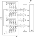
- FIGs. 3 and 4 illustrate one example of a DAC 320, a comparator circuitry 330, and a register circuitry 340 that enable a SAR-based ADC such as the one illustrated in FIG. 2 to determine two bits per clock cycle (i.e., in the first mode of operation).
- the DAC 320 inputs 10 register bits from a SAR (not shown, see register 210 in FIG. 2 ) as well as a common mode voltage V CM , two reference voltages V REF+ and V REF- , and the analog input voltage V IN that is being converted to a digital signal. While the example illustrated in FIG. 3 includes 10 register bits, any number of register bits may be used.
- the DAC 320 includes four capacitor banks, each including 11 capacitors. In each bank there is one capacitor for each register bit (C 9 for MSB - Co for LSB) and one "dummy" capacitor (C D ). The capacitance of the capacitors C 9 -C 0 increases by a factor of two so that C 1 has a capacitance that is twice the capacitance of Co, C 2 has a capacitance that is twice the capacitance of C 1 , and so on. The dummy capacitor has the same capacitance as Co.
- Each capacitor bank generates either a positive input voltage (e.g., V1 p or V2 p ) or a negative input voltage (V1 n r V2 n ) that is connected to either a positive or negative terminal of two of four comparators (labeled 0-3) in the comparator circuitry 330.
- V CM common mode voltage
- V CM common mode voltage
- the other terminal of each capacitor is connected through a three-pole switch to a selected one of VIN, VREF+, or VREF-.
- the switches are controlled by the DAC 320 to first store VIN in the capacitors and then, based on the result of each successive comparison operation, connect each capacitor to either VREF+ or VREF-.
- the DAC 320 controls the switches in each bank to selectively connect and disconnect the capacitors to the different potentials to generate the a next desired positive input voltages and negative input voltages (e.g., V CMP_p_k and VcMP_n_k) to be input to each comparator.
- Comparator 0's RES 0 indicates a value for the MSB bit in the pair (e.g., which half of the range the value for the two bits falls).
- Comparator 1's RES 1 indicates a value for the LSB in the pair when the MSB of the pair is 1.
- Comparator 2's RES 2 indicates a value for the LSB when the MSB of the pair is 0.
- Comparator 0's RES 0 indicates a value for the MSB bit in the pair (e.g., which half of the range the value for the two bits falls).
- Comparator 1's RES 1 indicates a value for the LSB in the pair when the MSB of the pair is 1.
- Comparator 2's RES 2 indicates a value for the LSB when the MSB of the pair is 0.
- only using three comparators will cause an imbalance in the loading of the capacitor banks because only two of the three banks would experience the additional input impedance of a second comparator.
- a fourth comparator (labeled 3) can be added that is connected to the second capacitor bank symmetrically with respect to the first capacitor bank.
- the comparison result RES 3 generated by the fourth comparator is not needed to determine register bit values, however, RES 3 can be used to increase SNR in LSB determination during the second mode of operation as will be described in more detail with reference to FIG. 4 .
- the design illustrated in FIG. 3 is extended to include more capacitor banks and more comparators may be used to enable the ADC to determine 3 or more bit values in a single cycle during the first mode of operation.
- FIG. 4 illustrates the register circuitry 340 operating in the first mode, the second mode, and at end of conversion (EOC).
- the register circuitry 340 inputs the results of the three comparators (RESo to RES 2 ) and, if used, the result of the optional fourth comparator RES 3 .
- there are 10 register bits and in the first mode of operation, the eight MSBs are determined, two bits per clock cycle. In the second mode of operation, the two LSBs are determined, one bit per clock cycle. In other examples, more or less MSBs and/or LSBs can be determined during the first and/or second mode of operation.
- the register circuitry 340 determines two MSB values (D9 and D8 are shown as an example) based on the results of three comparators as described above with reference to FIG. 3 .
- the comparators in the comparator circuitry 330 are performing comparison operations using positive input voltages and negative input voltages.
- the register circuitry 340 is performing a sorting operation based on the threshold determinations communicated by the comparison results.
- the ADC operates in the first mode for four cycles.
- the DAC 330 ( FIG. 3 ) sets the positive input voltages equal and the negative input voltages equal for the comparators. Each comparator thus determines a redundant comparison value for a single bit.
- the register circuitry 340 determines the value of one register bit (e.g., first LSB+1 then LSB) in a cycle by setting the register bit equal to the most popular/majority comparison result (i.e., 1 or 0) as between the three comparison results. An odd number of comparison results are used to determine the register bit values to avoid a tie situation. In this manner, redundant results can be used to improve the reliability of the register bit LSBs (leading to higher SNR of the complete ADC).
- the register circuitry 440 also stores the redundant comparison result for each comparator, including the fourth load balancing comparator when used.
- the ADC operates in the second mode for two cycles.
- the register circuitry 340 After values for all ten register bits have been determined, the register circuitry 340 generates D OUT based on the register bits as follows.
- the register circuitry 340 inputs three sequences of bits (or four if the optional fourth comparator is used). Each sequence includes the MSB values, in common, that were determined in the first mode of operation. Each sequence includes the stored LSB values for one of the comparators. Thus, in the example of FIG. 4 , each sequence includes 10 bit values.
- the register circuitry 340 generates D OUT based on the sequences. In one example, the register circuitry 340 adds the sequences to generate a 12 bit "sum" sequence that is D OUT . The 12 bit sequence corresponds to a 10 bit integer and a 2 bit (LSBs) fractional value. In other examples, the register circuitry 340 averages the sequences and rounds to a 10 bit integer to generate D OUT .
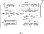
- FIG. 5 illustrates a flow diagram outlining one embodiment of a method 500 to convert an analog voltage into a digital signal comprising a binary sequence that represents the voltage.
- the method 500 may be performed, for example, by the ADC 200 or 300 of FIGs. 2-4 .
- the method includes, at 510, inputting a next analog voltage to be converted.
- a determination is made as to whether all MSB values in a register have been determined (e.g., if the ADC is operating in the first mode). If all MSB values have not been determined, at 530 in a single cycle M comparators are used to determine values for a next two or more of consecutive most significant bits (MSBs) in the register based on the analog voltage and register bit values stored in the register.
- MSBs most significant bits
- the method includes determining at least M redundant values for a next single bit in the least significant bits (LSBs) in the register using the M comparators.
- a value for the LSB is determined based on the at least M redundant values.
- a determination is made as to whether all LSB values have been determined. If so, at 570, the method includes generating the digital signal based on the MSBs and the LSBs (e.g., the register bit values) stored in the register.
- a SAR-based ADC that determines values for MSBs two or more bits at a time with a plurality of comparators and then determines redundant values for LSBs using the plurality of comparators provides faster analog to digital conversion time (as compared to single bit per cycle ADCs) while also enhancing the SNR of the analog to digital conversion.
- the additional comparator may be used to further increase the SNR of the SAR-based ADC when determining the LSB value(s).
- Examples herein can include subject matter such as a method, means for performing acts or blocks of the method, at least one machine-readable medium including executable instructions that, when performed by a machine (e.g., a processor with memory or the like) cause the machine to perform acts of the method or of an apparatus or system for converting an analog voltage into a binary sequence that represents the voltage according to embodiments and examples described.
- a machine e.g., a processor with memory or the like
- An example is a method to convert an analog voltage into a binary sequence that represents the voltage, including receiving the analog voltage and then operating in two modes.
- M comparators are used to determine values for a next two or more of consecutive most significant bits (MSBs) in a register based on the analog voltage and register bit values stored in the register. M is equal to or greater than 3.
- MSBs most significant bits
- M is equal to or greater than 3.
- LSB next least significant bit
- the binary sequence is generated based at least on the MSBs and the LSBs in the register.
- An example includes determining the values for the next two or more of consecutive MSBs in the register includes: with the M comparators, performing different M comparison operations to generate M comparison results, wherein each comparison operation compares a respective positive input voltage to a respective negative input voltage to generate a respective comparison result, wherein each of the M comparators compares a different combination of positive input voltage and negative input voltage as compared to the others of the M comparators; and generating the values for the next two or more consecutive MSBs based on the M comparison results.
- An example includes determining at least M redundant values for a single LSB in the register includes, with the at least M comparators, performing at least M comparison operations, wherein each comparison operation compares a positive input voltage and negative input voltage having a same differential to generate the M redundant comparison results.
- An example includes determining the value for the next LSB based on the three redundant comparison results includes selecting a redundant comparison result generated by a majority of the M comparators.
- An example further including: for each of the M comparators, generating a sequence of N bits that includes the MSB values and a redundant comparison result for the LSB generated by the comparator; and generating the binary sequence based at least on the M sequences of N bits.
- An example includes adding the M sequences to generate a sum sequence including more than N bits; and determining the binary sequence based at least on the sum sequence.
- An example further including, in the second mode, in each cycle: determining M+1 redundant comparison results for the next single bit in the least significant bits (LSBs) in the register using the M comparators and an additional comparator; and determining a value for the next LSB based on the M+1 redundant comparison results.
- LSBs least significant bits
- An example is an analog-to-digital converter (ADC) configured to convert an analog voltage into a binary sequence that represents the voltage, including: a register configured to store bit values; register circuitry configured to determine the bit values; M comparators; and ADC control circuitry configured to control the ADC to operate in a first mode or a second mode.
- the register circuitry In the first mode, in each cycle, the register circuitry is configured to determine values for a next two or more of consecutive most significant bits (MSBs) in the register based on comparison results of the comparators; and in the second mode, in each cycle, the register circuitry is configured to determine a value for a next single bit in the least significant bits (LSBs) in the register based on the at least M redundant comparison results.
- the register circuitry is configured to generate the binary sequence based on the MSBs and the LSBs in the register.
- An example further including digital-to-analog converter (DAC) circuitry configured to generate a positive input voltage and a negative input voltage pair for each comparator based on a digital sample of the analog voltage and the bit values in the register.
- DAC digital-to-analog converter
- An example includes in the first mode, in each cycle, the DAC circuitry being configured to generate a different positive input voltage and negative input voltage pair for each comparator based on the analog voltage and register bit values stored in the register, such that each of the M comparators compares a different combination of positive input voltage and negative input voltage as compared to the others of the M comparators.
- An example includes in the second mode, in each cycle, the DAC circuitry being configured to generate a positive input voltage and negative input voltage pair having a same differential for each comparator based on the analog voltage and register bit values stored in the register, such that the comparators generate M redundant comparison results.
- An example includes the register circuitry being configured to determine the value for the next LSB by selecting a redundant comparison result generated by a majority of the at least M comparators.
- An example includes the register circuitry being further configured to: for each of the at least M comparators, generate a sequence of N bits that includes the MSB values and a redundant comparison result for the LSB generated by the comparator; and generate the binary sequence based at least on the at least M sequences of N bits.
- An example includes the register circuitry being further configured to: add the at least M sequences to generate a sum sequence including more than N bits; and determine the binary sequence based at least on the sum sequence.
- An example further including: an additional comparator such that the total number of comparators is M+1; wherein in the second mode, in each cycle, the DAC circuitry is configured to generate the same positive input voltage and negative input voltage pair for each of the M+1 comparators based on the analog voltage and register bit values stored in the register, such that the comparators generate M+1 redundant comparison results; and the register circuitry is configured to determine a value for the next LSB based on the M+1 redundant comparison results.
- An example is ADC control circuitry configured to, in response to receiving an analog voltage for conversion to a binary sequence: control DAC circuitry and register circuitry to operate in a first mode and a second mode.
- the DAC circuitry In the first mode, in each cycle, the DAC circuitry generates a different positive input voltage and negative input voltage pair for each of M comparators based on the analog voltage and register bit values stored in a register, such that each of the M comparators compares a different combination of positive input voltage and negative input voltage as compared to the others of the M comparators.
- the ADC control circuitry is configured to control the register circuitry to determine values for a next two or more of consecutive most significant bits (MSBs) in the register based on the M comparison results.
- MSBs most significant bits
- the ADC control circuitry is configured to control the DAC circuitry to operate in the second mode wherein, in each cycle, the DAC circuitry is configured to generate a positive input voltage and negative input voltage pair having a same differential for each of the M comparators based on the analog voltage and register bit values stored in the register, such that the comparators generate M redundant comparison results.
- the ADC control circuitry is configured to control the register circuitry to operate in the second mode, wherein, in each cycle, the register circuitry determines a value for a next LSB based on the M redundant comparison results; and in response to a predetermined number of LSBs being determined, control the register circuitry to generate the binary sequence based at least on the MSBs and LSBs in the register.
- An example further configured, in the second mode, to control the register circuitry to determine the value for the next LSB by selecting a redundant comparison result generated by a majority of the at least M comparators.
- An example further configured, in response to the predetermined number of LSBs being determined, to control the register circuitry to: for each of the at least M comparators, generate a sequence of N bits that includes the MSB values and a redundant comparison result for the LSB generated by the comparator; and generate the binary sequence based at least on the at least M sequences of N bits.
- An example further configured, in the second mode, to control the register circuitry to add the at least M sequences to generate a sum sequence including more than N bits; and determine the binary sequence based at least on the sum sequence.
- An example further configured to, in the second mode, in each cycle: control the DAC circuitry to generate a positive input voltage and negative input voltage having a same differential for each of M+1 comparators based on the analog voltage and register bit values stored in the register, such that comparators generate M+1 redundant comparison results; and control the register circuitry to determine a value for the next LSB based on the M+1 redundant comparison results.
- An example is an apparatus configured to convert an analog voltage into a binary sequence that represents the voltage, including: means for receiving the analog voltage; means for using M comparators to determine, in a first mode, in each cycle, values for a next two or more of consecutive most significant bits (MSBs) in a register based on the analog voltage and register bit values stored in the register, wherein M is equal to or greater than 3; means for using M comparators to determine, in a second mode, in each cycle, at least M redundant comparison results using the M comparators; and a value for a next least significant bit (LSB) in the register based on the at least M redundant comparison results; and means for generating the binary sequence based at least on the MSBs and the LSBs in the register.
- MSBs most significant bits
- An example includes the means for using M comparators to determine the values for the next two or more of consecutive MSBs in the register including: means for using the M comparators to perform different M comparison operations to generate M comparison results, wherein each comparison operation compares a respective positive input voltage to a respective negative input voltage to generate a respective comparison result, wherein each of the M comparators compares a different combination of positive input voltage and negative input voltage as compared to the others of the M comparators; and means for generating the values for the next two or more consecutive MSBs based on the M comparison results.
- An example includes the means for determining at least M redundant values for a single LSB in the register including, means for using the at least M comparators to perform at least M comparison operations, wherein each comparison operation compares a positive input voltage and negative input voltage having a same differential to generate the M redundant comparison results.
- An example includes the means for generating the binary sequence including means for generating, for each of the M comparators, a sequence of N bits that includes the MSB values and a redundant comparison result for the LSB generated by the comparator; and means for generating the binary sequence based at least on the M sequences of N bits.
- Computer-readable media includes both computer storage media and communication media including any medium that facilitates transfer of a computer program from one place to another.
- a storage media may be any available media that can be accessed by a general purpose or special purpose computer.
- various illustrative logics, logical blocks, modules, and circuits described in connection with aspects disclosed herein may be implemented or performed with a general purpose processor, a digital signal processor (DSP), an application specific integrated circuit (ASIC), a field programmable gate array (FPGA) or other programmable logic device, discrete gate or transistor logic, discrete hardware components, or any combination thereof designed to perform functions described herein.
- DSP digital signal processor
- ASIC application specific integrated circuit
- FPGA field programmable gate array
- a general-purpose processor may be a microprocessor, but, in the alternative, processor may be any conventional processor, controller, microcontroller, or state machine.
- a processor may also be implemented as a combination of computing devices, for example, a combination of a DSP and a microprocessor, a plurality of microprocessors, one or more microprocessors in conjunction with a DSP core, or any other such configuration. Additionally, at least one processor may include one or more modules operable to perform one or more of the acts and/or actions described herein.
- modules e.g., procedures, functions, and so on
- Software codes may be stored in memory units and executed by processors.
- Memory unit may be implemented within processor or external to processor, in which case memory unit can be communicatively coupled to processor through various means as is known in the art.
- at least one processor may include one or more modules operable to perform functions described herein.
- a software module may reside in RAM memory, flash memory, ROM memory, EPROM memory, EEPROM memory, registers, a hard disk, a removable disk, a CD-ROM, or any other form of storage medium known in the art.
- An exemplary storage medium may be coupled to processor, such that processor can read information from, and write information to, storage medium.
- storage medium may be integral to processor.
- processor and storage medium may reside in an ASIC. Additionally, ASIC may reside in a user terminal.
- processor and storage medium may reside as discrete components in a user terminal.
- acts and/or actions of a method or algorithm may reside as one or any combination or set of codes and/or instructions on a machine-readable medium and/or computer readable medium, which may be incorporated into a computer program product.
Landscapes
- Engineering & Computer Science (AREA)
- Theoretical Computer Science (AREA)
- Physics & Mathematics (AREA)
- Nonlinear Science (AREA)
- Analogue/Digital Conversion (AREA)
Claims (13)
- Procédé pour convertir une tension analogique en une séquence binaire qui représente la tension analogique, comprenant le faire de :recevoir la tension analogique ;générer une paire de tensions d'entrée pour chacun des M comparateurs sur la base d'un échantillon numérique de la tension analogique et des valeurs de bit stockées dans un registre (210), dans lequel M est égal ou supérieur à 3 ;dans un premier mode, à chaque cycle, utiliser les M comparateurs pour déterminer des valeurs pour des deux prochains ou plus parmi des bits les plus significatifs, MSBs, consécutifs dans le registre (210) sur la base de la tension analogique et des valeurs de bit stockées dans le registre (210) ;dans un deuxième mode, à chaque cycle :déterminer au moins des M résultats de comparaison redondants en utilisant les M comparateurs ; etdéterminer une valeur pour un prochain bit le moins significatif, LSB, dans le registre (210) sur la base des au moins M résultats de comparaison redondants, dans lequel la paire de tensions d'entrée pour chaque comparateur est générée de manière à avoir un même différentiel dans le deuxième mode tel que les M résultats de comparaison redondants de tous les M comparateurs sont utilisés pour déterminer la valeur pour le prochain LSB ; etgénérer la séquence binaire sur la base au moins des MSBs et des LSBs dans le registre (210).
- Procédé selon la revendication 1, dans lequel le fait de déterminer les valeurs pour les deux prochains ou plus parmi des MSBs consécutifs dans le registre (210) comprend le fait de :avec les M comparateurs, effectuer des M opérations de comparaison différentes pour générer M résultats de comparaison, dans lequel chaque opération de comparaison compare une tension d'entrée positive respective à une tension d'entrée négative respective pour générer un résultat de comparaison respectif, dans lequel chacun des M comparateurs compare une combinaison différente de tension d'entrée positive et tension d'entrée négative par rapport aux autres des M comparateurs ; etgénérer les valeurs pour les deux prochains ou plus MSBs consécutifs sur la base des M résultats de comparaison.
- Procédé selon la revendication 1, dans lequel le fait de déterminer la valeur pour le prochain LSB sur la base des M résultats de comparaison redondants comprend le fait de sélectionner un résultat de comparaison redondant généré par une majorité des M comparateurs.
- Procédé selon l'une des revendications 1-3, comprenant en outre le fait de :pour chacun des M comparateurs, générer une séquence de N bits qui comprend des valeurs MSB et un résultat de comparaison redondant pour un LSB généré par le comparateur ;générer la séquence binaire sur la base au moins des M séquences de N bits.
- Procédé selon la revendication 4, comprenant en outre le fait de :ajouter les M séquences pour générer une séquence de somme comprenant plus de N bits ; etdéterminer la séquence binaire sur la base au moins de la séquence de somme.
- Procédé selon l'une des revendications 1-3, comprenant en outre, dans le deuxième mode, à chaque cycle :déterminer M+1 résultats de comparaison redondants pour le prochain bit unique dans les bits les moins significatifs, LSBs, dans le registre (210) en utilisant les M comparateurs et un comparateur supplémentaire ; etdéterminer une valeur pour le prochain LSB sur la base des M+1 résultats de comparaison redondants.
- Convertisseur analogique-numérique, CAN, configuré pour convertir une tension analogique en une séquence binaire qui représente la tension analogique, comprenant :un registre (210) configuré pour stocker des valeurs de bit ;un circuit de registre (240) configuré pour déterminer les valeurs de bit ;un circuit de comparateur (230) comprenant des M comparateurs, dans lequel M est égal ou supérieur à 3 ;un circuit de convertisseur numérique-analogique, CNA, (220) configuré pour générer une paire de tensions d'entrée pour chacun comparateur sur la base d'un échantillon numérique de la tension analogique et des valeurs de bit dans un registre (210) ; etun circuit de commande CAN (250) configuré pour commander le CAN pour qu'il fonctionne dans un premier mode ou un deuxième mode, dans lequel :dans le premier mode, à chaque cycle, le circuit de registre (240) est configuré pour déterminer des valeurs pour des deux prochains ou plus parmi des bits les plus significatifs, MSBs, consécutifs dans le registre (210) sur la base des résultats de comparaison des comparateurs ; etdans le deuxième mode, à chaque cycle, le circuit de registre (240) est configuré pour déterminer une valeur pour un prochain bit unique dans des bits les moins significatifs, LSBs, dans le registre (210) sur la base des au moins M résultats de comparaison redondants, dans lequel le circuit CNA (220) est configuré pour générer la paire de tensions d'entrée ayant un même différentiel pour chaque comparateur dans le deuxième mode tel que les M résultats de comparaison redondants de tous les M comparateurs sont utilisés pour déterminer la valeur pour le prochain LSB ; etdans lequel le circuit de registre (240) est configuré pour générer la séquence binaire sur la base des MSBs et des LSBs dans le registre (210).
- Le CAN selon la revendication 7, dans lequel le circuit CNA (220) est configuré pour générer une paire de tension d'entrée positive et tension d'entrée négative pour chacun comparateur sur la base d'un échantillon numérique de la tension analogique et des valeurs de bit dans le registre (210).
- Le CAN selon la revendication 8, dans lequel dans le premier mode, à chaque cycle, le circuit CNA (220) est configuré pour générer une paire de tension d'entrée positive et de tension d'entrée négative différente pour chaque comparateur sur la base de la tension analogique et des valeurs de bit de registre stockées dans le registre (210), de telle sorte que chacun des M comparateurs compare une combinaison différente de tension d'entrée positive et de tension d'entrée négative par rapport aux autres des M comparateurs.
- Le CAN selon la revendication 8, dans lequel le circuit de registre (240) est configuré pour déterminer la valeur pour le prochain LSB en sélectionnant un résultat de comparaison redondant généré par une majorité des au moins M comparateurs.
- Le CAN selon l'une des revendications 7-10, dans lequel le circuit de registre (240) est en outre configuré pour :pour chacun des au moins M comparateurs, générer une séquence de N bits qui comprend les valeurs MSB et un résultat de comparaison redondant pour le LSB généré par le comparateur ;générer la séquence binaire sur la base au moins des au moins M séquences de N bits.
- Le CAN selon la revendication 11, dans lequel le circuit de registre (240) est en outre configuré pour :ajouter les au moins M séquences pour générer une séquence de somme comprenant plus de N bits ; etdéterminer la séquence binaire sur la base au moins de la séquence de somme.
- Le CAN selon l'une des revendications 7-10, comprenant en outre :un comparateur supplémentaire tel que le nombre total de comparateurs soit M+1 ;dans lequel, dans le deuxième mode, à chaque cycle :le circuit CNA (220) est configuré pour générer la même paire de tension d'entrée positive et de tension d'entrée négative pour chacun des M+1 comparateurs sur la base de la tension analogique et des valeurs de bit de registre stockées dans le registre (210), de sorte que les comparateurs génèrent M+1 résultats de comparaison redondants ; etle circuit de registre (240) est configuré pour déterminer une valeur pour le prochain LSB sur la base des M+1 résultats de comparaison redondants.
Applications Claiming Priority (1)
| Application Number | Priority Date | Filing Date | Title |
|---|---|---|---|
| US15/684,378 US10020816B1 (en) | 2017-08-23 | 2017-08-23 | Hybrid successive approximation register analog to digital converter |
Publications (2)
| Publication Number | Publication Date |
|---|---|
| EP3447921A1 EP3447921A1 (fr) | 2019-02-27 |
| EP3447921B1 true EP3447921B1 (fr) | 2021-09-01 |
Family
ID=62749665
Family Applications (1)
| Application Number | Title | Priority Date | Filing Date |
|---|---|---|---|
| EP18186725.0A Active EP3447921B1 (fr) | 2017-08-23 | 2018-07-31 | Convertisseur analogique-numérique hybride à enregistrement d'approximation successive |
Country Status (2)
| Country | Link |
|---|---|
| US (1) | US10020816B1 (fr) |
| EP (1) | EP3447921B1 (fr) |
Families Citing this family (8)
| Publication number | Priority date | Publication date | Assignee | Title |
|---|---|---|---|---|
| US10491231B2 (en) * | 2018-02-16 | 2019-11-26 | Sensors Unlimited, Inc. | Reconfigurable ADC architecture for imaging-based applications |
| CN112514260A (zh) | 2018-08-03 | 2021-03-16 | 拉姆伯斯公司 | 用于逐次逼近型寄存器模数转换器的偏移校准 |
| US10484001B1 (en) * | 2018-10-31 | 2019-11-19 | Texas Instruments Incorporated | Multi-bit successive-approximation register analog-to-digital converter |
| WO2020200480A1 (fr) * | 2019-04-05 | 2020-10-08 | Telefonaktiebolaget Lm Ericsson (Publ) | Can sar avec comparateurs de haute et basse précision alternants et attribution irrégulière de redondance |
| CN110138387B (zh) * | 2019-06-05 | 2020-11-03 | 中国电子科技集团公司第二十四研究所 | 一种基于单通道时间交织采样的sar adc及采样方法 |
| TWI792438B (zh) * | 2021-07-22 | 2023-02-11 | 瑞昱半導體股份有限公司 | 訊號轉換裝置、動態元件匹配電路與動態元件匹配方法 |
| US11811416B2 (en) | 2021-12-14 | 2023-11-07 | International Business Machines Corporation | Energy-efficient analog-to-digital conversion in mixed signal circuitry |
| CN115001499A (zh) * | 2022-05-31 | 2022-09-02 | 共模半导体技术(苏州)有限公司 | 一种具有冗余的逐次逼近模数转换电路 |
Family Cites Families (5)
| Publication number | Priority date | Publication date | Assignee | Title |
|---|---|---|---|---|
| US3581304A (en) * | 1967-05-16 | 1971-05-25 | Singer General Precision | Analog-to-digital cyclic forward feed successive approximation conversion equipment |
| FR2427012A1 (fr) * | 1978-05-24 | 1979-12-21 | Labo Electronique Physique | Convertisseur analogique-numerique binaire |
| KR101007063B1 (ko) * | 2008-10-31 | 2011-01-12 | 한국과학기술원 | Sar 방식의 아날로그/디지털 변환기의 디지털 에러수정 방법 및 장치 |
| EP2546992B1 (fr) * | 2011-07-13 | 2014-03-05 | Imec | Convertisseur analogique/numérique stochastique et son procédé d'utilisation |
| ITMI20132037A1 (it) * | 2013-12-06 | 2015-06-07 | St Microelectronics Int Nv | Metodo per la correzione di errori digitali per convertitore analogico digitale binario ad approssimazioni successive. |
-
2017
- 2017-08-23 US US15/684,378 patent/US10020816B1/en active Active
-
2018
- 2018-07-31 EP EP18186725.0A patent/EP3447921B1/fr active Active
Also Published As
| Publication number | Publication date |
|---|---|
| US10020816B1 (en) | 2018-07-10 |
| EP3447921A1 (fr) | 2019-02-27 |
Similar Documents
| Publication | Publication Date | Title |
|---|---|---|
| EP3447921B1 (fr) | Convertisseur analogique-numérique hybride à enregistrement d'approximation successive | |
| US8390501B2 (en) | Successive approximation register ADC with a window predictive function | |
| US9362939B1 (en) | Reduction of input dependent capacitor DAC switching current in flash-SAR analog-to-digital converters | |
| EP2624458B1 (fr) | Convertisseur analogique-numérique à registre à approximations successives | |
| US8310388B2 (en) | Subrange analog-to-digital converter and method thereof | |
| TWI454064B (zh) | 具輔助預測電路之逐漸趨近式類比數位轉換器及其方法 | |
| US6958722B1 (en) | SAR ADC providing digital codes with high accuracy and high throughput performance | |
| US9774345B1 (en) | Successive approximation register analog-to-digital converter | |
| US8599059B1 (en) | Successive approximation register analog-digital converter and method for operating the same | |
| US8525720B2 (en) | Non-binary successive approximation analog to digital converter | |
| US8854243B2 (en) | AD converter circuit and ad conversion method | |
| EP3090488B1 (fr) | Combinaison d'un can grossier et d'un can à sar | |
| US9432046B1 (en) | Successive approximation analog-to-digital converter | |
| US9496888B1 (en) | Asynchronous SAR ADC with binary scaled redundancy | |
| TW201524133A (zh) | 連續近似式類比數位轉換器 | |
| TWI792438B (zh) | 訊號轉換裝置、動態元件匹配電路與動態元件匹配方法 | |
| CN105556847A (zh) | 流水线逐次近似模数转换器 | |
| CN113271105B (zh) | 带有可变采样电容器的sar adc | |
| CN109937536A (zh) | 模数转换器 | |
| WO2020200480A1 (fr) | Can sar avec comparateurs de haute et basse précision alternants et attribution irrégulière de redondance | |
| US8508398B1 (en) | Systems for comparator offset cancellation in successive-approximation-register analog-to-digital converters | |
| CN117560007A (zh) | 一种逐次逼近型模数转换器 | |
| CN108141219A (zh) | 用于模数转换的方法和模数转换器 | |
| JP2014236373A (ja) | A/d変換装置 | |
| Dhage et al. | Design of power efficient hybrid flash-successive approximation register analog to digital converter |
Legal Events
| Date | Code | Title | Description |
|---|---|---|---|
| PUAI | Public reference made under article 153(3) epc to a published international application that has entered the european phase |
Free format text: ORIGINAL CODE: 0009012 |
|
| STAA | Information on the status of an ep patent application or granted ep patent |
Free format text: STATUS: THE APPLICATION HAS BEEN PUBLISHED |
|
| AK | Designated contracting states |
Kind code of ref document: A1 Designated state(s): AL AT BE BG CH CY CZ DE DK EE ES FI FR GB GR HR HU IE IS IT LI LT LU LV MC MK MT NL NO PL PT RO RS SE SI SK SM TR |
|
| AX | Request for extension of the european patent |
Extension state: BA ME |
|
| STAA | Information on the status of an ep patent application or granted ep patent |
Free format text: STATUS: REQUEST FOR EXAMINATION WAS MADE |
|
| 17P | Request for examination filed |
Effective date: 20190827 |
|
| RBV | Designated contracting states (corrected) |
Designated state(s): AL AT BE BG CH CY CZ DE DK EE ES FI FR GB GR HR HU IE IS IT LI LT LU LV MC MK MT NL NO PL PT RO RS SE SI SK SM TR |
|
| RAP1 | Party data changed (applicant data changed or rights of an application transferred) |
Owner name: INTEL CORPORATION |
|
| GRAP | Despatch of communication of intention to grant a patent |
Free format text: ORIGINAL CODE: EPIDOSNIGR1 |
|
| STAA | Information on the status of an ep patent application or granted ep patent |
Free format text: STATUS: GRANT OF PATENT IS INTENDED |
|
| INTG | Intention to grant announced |
Effective date: 20200930 |
|
| GRAJ | Information related to disapproval of communication of intention to grant by the applicant or resumption of examination proceedings by the epo deleted |
Free format text: ORIGINAL CODE: EPIDOSDIGR1 |
|
| STAA | Information on the status of an ep patent application or granted ep patent |
Free format text: STATUS: REQUEST FOR EXAMINATION WAS MADE |
|
| INTC | Intention to grant announced (deleted) | ||
| GRAP | Despatch of communication of intention to grant a patent |
Free format text: ORIGINAL CODE: EPIDOSNIGR1 |
|
| STAA | Information on the status of an ep patent application or granted ep patent |
Free format text: STATUS: GRANT OF PATENT IS INTENDED |
|
| INTG | Intention to grant announced |
Effective date: 20210322 |
|
| RAP1 | Party data changed (applicant data changed or rights of an application transferred) |
Owner name: MAXLINEAR ASIA SINGAPORE PRIVATE LIMITED |
|
| GRAS | Grant fee paid |
Free format text: ORIGINAL CODE: EPIDOSNIGR3 |
|
| GRAA | (expected) grant |
Free format text: ORIGINAL CODE: 0009210 |
|
| STAA | Information on the status of an ep patent application or granted ep patent |
Free format text: STATUS: THE PATENT HAS BEEN GRANTED |
|
| AK | Designated contracting states |
Kind code of ref document: B1 Designated state(s): AL AT BE BG CH CY CZ DE DK EE ES FI FR GB GR HR HU IE IS IT LI LT LU LV MC MK MT NL NO PL PT RO RS SE SI SK SM TR |
|
| REG | Reference to a national code |
Ref country code: GB Ref legal event code: FG4D |
|
| REG | Reference to a national code |
Ref country code: CH Ref legal event code: EP Ref country code: AT Ref legal event code: REF Ref document number: 1427304 Country of ref document: AT Kind code of ref document: T Effective date: 20210915 |
|
| REG | Reference to a national code |
Ref country code: DE Ref legal event code: R096 Ref document number: 602018022708 Country of ref document: DE |
|
| REG | Reference to a national code |
Ref country code: IE Ref legal event code: FG4D |
|
| REG | Reference to a national code |
Ref country code: LT Ref legal event code: MG9D |
|
| REG | Reference to a national code |
Ref country code: NL Ref legal event code: MP Effective date: 20210901 |
|
| PG25 | Lapsed in a contracting state [announced via postgrant information from national office to epo] |
Ref country code: RS Free format text: LAPSE BECAUSE OF FAILURE TO SUBMIT A TRANSLATION OF THE DESCRIPTION OR TO PAY THE FEE WITHIN THE PRESCRIBED TIME-LIMIT Effective date: 20210901 Ref country code: SE Free format text: LAPSE BECAUSE OF FAILURE TO SUBMIT A TRANSLATION OF THE DESCRIPTION OR TO PAY THE FEE WITHIN THE PRESCRIBED TIME-LIMIT Effective date: 20210901 Ref country code: HR Free format text: LAPSE BECAUSE OF FAILURE TO SUBMIT A TRANSLATION OF THE DESCRIPTION OR TO PAY THE FEE WITHIN THE PRESCRIBED TIME-LIMIT Effective date: 20210901 Ref country code: ES Free format text: LAPSE BECAUSE OF FAILURE TO SUBMIT A TRANSLATION OF THE DESCRIPTION OR TO PAY THE FEE WITHIN THE PRESCRIBED TIME-LIMIT Effective date: 20210901 Ref country code: FI Free format text: LAPSE BECAUSE OF FAILURE TO SUBMIT A TRANSLATION OF THE DESCRIPTION OR TO PAY THE FEE WITHIN THE PRESCRIBED TIME-LIMIT Effective date: 20210901 Ref country code: NO Free format text: LAPSE BECAUSE OF FAILURE TO SUBMIT A TRANSLATION OF THE DESCRIPTION OR TO PAY THE FEE WITHIN THE PRESCRIBED TIME-LIMIT Effective date: 20211201 Ref country code: LT Free format text: LAPSE BECAUSE OF FAILURE TO SUBMIT A TRANSLATION OF THE DESCRIPTION OR TO PAY THE FEE WITHIN THE PRESCRIBED TIME-LIMIT Effective date: 20210901 Ref country code: BG Free format text: LAPSE BECAUSE OF FAILURE TO SUBMIT A TRANSLATION OF THE DESCRIPTION OR TO PAY THE FEE WITHIN THE PRESCRIBED TIME-LIMIT Effective date: 20211201 |
|
| REG | Reference to a national code |
Ref country code: AT Ref legal event code: MK05 Ref document number: 1427304 Country of ref document: AT Kind code of ref document: T Effective date: 20210901 |
|
| PG25 | Lapsed in a contracting state [announced via postgrant information from national office to epo] |
Ref country code: PL Free format text: LAPSE BECAUSE OF FAILURE TO SUBMIT A TRANSLATION OF THE DESCRIPTION OR TO PAY THE FEE WITHIN THE PRESCRIBED TIME-LIMIT Effective date: 20210901 Ref country code: LV Free format text: LAPSE BECAUSE OF FAILURE TO SUBMIT A TRANSLATION OF THE DESCRIPTION OR TO PAY THE FEE WITHIN THE PRESCRIBED TIME-LIMIT Effective date: 20210901 Ref country code: GR Free format text: LAPSE BECAUSE OF FAILURE TO SUBMIT A TRANSLATION OF THE DESCRIPTION OR TO PAY THE FEE WITHIN THE PRESCRIBED TIME-LIMIT Effective date: 20211202 |
|
| PG25 | Lapsed in a contracting state [announced via postgrant information from national office to epo] |
Ref country code: AT Free format text: LAPSE BECAUSE OF FAILURE TO SUBMIT A TRANSLATION OF THE DESCRIPTION OR TO PAY THE FEE WITHIN THE PRESCRIBED TIME-LIMIT Effective date: 20210901 |
|
| PG25 | Lapsed in a contracting state [announced via postgrant information from national office to epo] |
Ref country code: IS Free format text: LAPSE BECAUSE OF FAILURE TO SUBMIT A TRANSLATION OF THE DESCRIPTION OR TO PAY THE FEE WITHIN THE PRESCRIBED TIME-LIMIT Effective date: 20220101 Ref country code: SM Free format text: LAPSE BECAUSE OF FAILURE TO SUBMIT A TRANSLATION OF THE DESCRIPTION OR TO PAY THE FEE WITHIN THE PRESCRIBED TIME-LIMIT Effective date: 20210901 Ref country code: SK Free format text: LAPSE BECAUSE OF FAILURE TO SUBMIT A TRANSLATION OF THE DESCRIPTION OR TO PAY THE FEE WITHIN THE PRESCRIBED TIME-LIMIT Effective date: 20210901 Ref country code: RO Free format text: LAPSE BECAUSE OF FAILURE TO SUBMIT A TRANSLATION OF THE DESCRIPTION OR TO PAY THE FEE WITHIN THE PRESCRIBED TIME-LIMIT Effective date: 20210901 Ref country code: PT Free format text: LAPSE BECAUSE OF FAILURE TO SUBMIT A TRANSLATION OF THE DESCRIPTION OR TO PAY THE FEE WITHIN THE PRESCRIBED TIME-LIMIT Effective date: 20220103 Ref country code: NL Free format text: LAPSE BECAUSE OF FAILURE TO SUBMIT A TRANSLATION OF THE DESCRIPTION OR TO PAY THE FEE WITHIN THE PRESCRIBED TIME-LIMIT Effective date: 20210901 Ref country code: EE Free format text: LAPSE BECAUSE OF FAILURE TO SUBMIT A TRANSLATION OF THE DESCRIPTION OR TO PAY THE FEE WITHIN THE PRESCRIBED TIME-LIMIT Effective date: 20210901 Ref country code: CZ Free format text: LAPSE BECAUSE OF FAILURE TO SUBMIT A TRANSLATION OF THE DESCRIPTION OR TO PAY THE FEE WITHIN THE PRESCRIBED TIME-LIMIT Effective date: 20210901 Ref country code: AL Free format text: LAPSE BECAUSE OF FAILURE TO SUBMIT A TRANSLATION OF THE DESCRIPTION OR TO PAY THE FEE WITHIN THE PRESCRIBED TIME-LIMIT Effective date: 20210901 |
|
| REG | Reference to a national code |
Ref country code: DE Ref legal event code: R097 Ref document number: 602018022708 Country of ref document: DE |
|
| PLBE | No opposition filed within time limit |
Free format text: ORIGINAL CODE: 0009261 |
|
| STAA | Information on the status of an ep patent application or granted ep patent |
Free format text: STATUS: NO OPPOSITION FILED WITHIN TIME LIMIT |
|
| PG25 | Lapsed in a contracting state [announced via postgrant information from national office to epo] |
Ref country code: IT Free format text: LAPSE BECAUSE OF FAILURE TO SUBMIT A TRANSLATION OF THE DESCRIPTION OR TO PAY THE FEE WITHIN THE PRESCRIBED TIME-LIMIT Effective date: 20210901 Ref country code: DK Free format text: LAPSE BECAUSE OF FAILURE TO SUBMIT A TRANSLATION OF THE DESCRIPTION OR TO PAY THE FEE WITHIN THE PRESCRIBED TIME-LIMIT Effective date: 20210901 |
|
| 26N | No opposition filed |
Effective date: 20220602 |
|
| PG25 | Lapsed in a contracting state [announced via postgrant information from national office to epo] |
Ref country code: SI Free format text: LAPSE BECAUSE OF FAILURE TO SUBMIT A TRANSLATION OF THE DESCRIPTION OR TO PAY THE FEE WITHIN THE PRESCRIBED TIME-LIMIT Effective date: 20210901 |
|
| PG25 | Lapsed in a contracting state [announced via postgrant information from national office to epo] |
Ref country code: MC Free format text: LAPSE BECAUSE OF FAILURE TO SUBMIT A TRANSLATION OF THE DESCRIPTION OR TO PAY THE FEE WITHIN THE PRESCRIBED TIME-LIMIT Effective date: 20210901 |
|
| REG | Reference to a national code |
Ref country code: CH Ref legal event code: PL |
|
| GBPC | Gb: european patent ceased through non-payment of renewal fee |
Effective date: 20220731 |
|
| REG | Reference to a national code |
Ref country code: BE Ref legal event code: MM Effective date: 20220731 |
|
| PG25 | Lapsed in a contracting state [announced via postgrant information from national office to epo] |
Ref country code: LU Free format text: LAPSE BECAUSE OF NON-PAYMENT OF DUE FEES Effective date: 20220731 Ref country code: LI Free format text: LAPSE BECAUSE OF NON-PAYMENT OF DUE FEES Effective date: 20220731 Ref country code: FR Free format text: LAPSE BECAUSE OF NON-PAYMENT OF DUE FEES Effective date: 20220731 Ref country code: CH Free format text: LAPSE BECAUSE OF NON-PAYMENT OF DUE FEES Effective date: 20220731 |
|
| PG25 | Lapsed in a contracting state [announced via postgrant information from national office to epo] |
Ref country code: GB Free format text: LAPSE BECAUSE OF NON-PAYMENT OF DUE FEES Effective date: 20220731 Ref country code: BE Free format text: LAPSE BECAUSE OF NON-PAYMENT OF DUE FEES Effective date: 20220731 |
|
| P01 | Opt-out of the competence of the unified patent court (upc) registered |
Effective date: 20230601 |
|
| PG25 | Lapsed in a contracting state [announced via postgrant information from national office to epo] |
Ref country code: IE Free format text: LAPSE BECAUSE OF NON-PAYMENT OF DUE FEES Effective date: 20220731 |
|
| PG25 | Lapsed in a contracting state [announced via postgrant information from national office to epo] |
Ref country code: HU Free format text: LAPSE BECAUSE OF FAILURE TO SUBMIT A TRANSLATION OF THE DESCRIPTION OR TO PAY THE FEE WITHIN THE PRESCRIBED TIME-LIMIT; INVALID AB INITIO Effective date: 20180731 |
|
| PG25 | Lapsed in a contracting state [announced via postgrant information from national office to epo] |
Ref country code: MK Free format text: LAPSE BECAUSE OF FAILURE TO SUBMIT A TRANSLATION OF THE DESCRIPTION OR TO PAY THE FEE WITHIN THE PRESCRIBED TIME-LIMIT Effective date: 20210901 Ref country code: CY Free format text: LAPSE BECAUSE OF FAILURE TO SUBMIT A TRANSLATION OF THE DESCRIPTION OR TO PAY THE FEE WITHIN THE PRESCRIBED TIME-LIMIT Effective date: 20210901 |
|
| PG25 | Lapsed in a contracting state [announced via postgrant information from national office to epo] |
Ref country code: TR Free format text: LAPSE BECAUSE OF FAILURE TO SUBMIT A TRANSLATION OF THE DESCRIPTION OR TO PAY THE FEE WITHIN THE PRESCRIBED TIME-LIMIT Effective date: 20210901 |
|
| PG25 | Lapsed in a contracting state [announced via postgrant information from national office to epo] |
Ref country code: MT Free format text: LAPSE BECAUSE OF FAILURE TO SUBMIT A TRANSLATION OF THE DESCRIPTION OR TO PAY THE FEE WITHIN THE PRESCRIBED TIME-LIMIT Effective date: 20210901 |
|
| PGFP | Annual fee paid to national office [announced via postgrant information from national office to epo] |
Ref country code: DE Payment date: 20250729 Year of fee payment: 8 |