EP3451321B1 - Elektrolumineszente anzeigevorrichtung und ansteuerungsverfahren dafür - Google Patents
Elektrolumineszente anzeigevorrichtung und ansteuerungsverfahren dafür Download PDFInfo
- Publication number
- EP3451321B1 EP3451321B1 EP18191531.5A EP18191531A EP3451321B1 EP 3451321 B1 EP3451321 B1 EP 3451321B1 EP 18191531 A EP18191531 A EP 18191531A EP 3451321 B1 EP3451321 B1 EP 3451321B1
- Authority
- EP
- European Patent Office
- Prior art keywords
- transistor
- voltage
- scan
- gate
- electrode
- Prior art date
- Legal status (The legal status is an assumption and is not a legal conclusion. Google has not performed a legal analysis and makes no representation as to the accuracy of the status listed.)
- Active
Links
Images






Classifications
-
- G—PHYSICS
- G09—EDUCATION; CRYPTOGRAPHY; DISPLAY; ADVERTISING; SEALS
- G09G—ARRANGEMENTS OR CIRCUITS FOR CONTROL OF INDICATING DEVICES USING STATIC MEANS TO PRESENT VARIABLE INFORMATION
- G09G3/00—Control arrangements or circuits, of interest only in connection with visual indicators other than cathode-ray tubes
- G09G3/20—Control arrangements or circuits, of interest only in connection with visual indicators other than cathode-ray tubes for presentation of an assembly of a number of characters, e.g. a page, by composing the assembly by combination of individual elements arranged in a matrix no fixed position being assigned to or needed to be assigned to the individual characters or partial characters
- G09G3/22—Control arrangements or circuits, of interest only in connection with visual indicators other than cathode-ray tubes for presentation of an assembly of a number of characters, e.g. a page, by composing the assembly by combination of individual elements arranged in a matrix no fixed position being assigned to or needed to be assigned to the individual characters or partial characters using controlled light sources
- G09G3/30—Control arrangements or circuits, of interest only in connection with visual indicators other than cathode-ray tubes for presentation of an assembly of a number of characters, e.g. a page, by composing the assembly by combination of individual elements arranged in a matrix no fixed position being assigned to or needed to be assigned to the individual characters or partial characters using controlled light sources using electroluminescent panels
- G09G3/32—Control arrangements or circuits, of interest only in connection with visual indicators other than cathode-ray tubes for presentation of an assembly of a number of characters, e.g. a page, by composing the assembly by combination of individual elements arranged in a matrix no fixed position being assigned to or needed to be assigned to the individual characters or partial characters using controlled light sources using electroluminescent panels semiconductive, e.g. using light-emitting diodes [LED]
- G09G3/3208—Control arrangements or circuits, of interest only in connection with visual indicators other than cathode-ray tubes for presentation of an assembly of a number of characters, e.g. a page, by composing the assembly by combination of individual elements arranged in a matrix no fixed position being assigned to or needed to be assigned to the individual characters or partial characters using controlled light sources using electroluminescent panels semiconductive, e.g. using light-emitting diodes [LED] organic, e.g. using organic light-emitting diodes [OLED]
- G09G3/3266—Details of drivers for scan electrodes
-
- G—PHYSICS
- G09—EDUCATION; CRYPTOGRAPHY; DISPLAY; ADVERTISING; SEALS
- G09G—ARRANGEMENTS OR CIRCUITS FOR CONTROL OF INDICATING DEVICES USING STATIC MEANS TO PRESENT VARIABLE INFORMATION
- G09G3/00—Control arrangements or circuits, of interest only in connection with visual indicators other than cathode-ray tubes
- G09G3/20—Control arrangements or circuits, of interest only in connection with visual indicators other than cathode-ray tubes for presentation of an assembly of a number of characters, e.g. a page, by composing the assembly by combination of individual elements arranged in a matrix no fixed position being assigned to or needed to be assigned to the individual characters or partial characters
- G09G3/22—Control arrangements or circuits, of interest only in connection with visual indicators other than cathode-ray tubes for presentation of an assembly of a number of characters, e.g. a page, by composing the assembly by combination of individual elements arranged in a matrix no fixed position being assigned to or needed to be assigned to the individual characters or partial characters using controlled light sources
- G09G3/30—Control arrangements or circuits, of interest only in connection with visual indicators other than cathode-ray tubes for presentation of an assembly of a number of characters, e.g. a page, by composing the assembly by combination of individual elements arranged in a matrix no fixed position being assigned to or needed to be assigned to the individual characters or partial characters using controlled light sources using electroluminescent panels
- G09G3/32—Control arrangements or circuits, of interest only in connection with visual indicators other than cathode-ray tubes for presentation of an assembly of a number of characters, e.g. a page, by composing the assembly by combination of individual elements arranged in a matrix no fixed position being assigned to or needed to be assigned to the individual characters or partial characters using controlled light sources using electroluminescent panels semiconductive, e.g. using light-emitting diodes [LED]
- G09G3/3208—Control arrangements or circuits, of interest only in connection with visual indicators other than cathode-ray tubes for presentation of an assembly of a number of characters, e.g. a page, by composing the assembly by combination of individual elements arranged in a matrix no fixed position being assigned to or needed to be assigned to the individual characters or partial characters using controlled light sources using electroluminescent panels semiconductive, e.g. using light-emitting diodes [LED] organic, e.g. using organic light-emitting diodes [OLED]
- G09G3/3225—Control arrangements or circuits, of interest only in connection with visual indicators other than cathode-ray tubes for presentation of an assembly of a number of characters, e.g. a page, by composing the assembly by combination of individual elements arranged in a matrix no fixed position being assigned to or needed to be assigned to the individual characters or partial characters using controlled light sources using electroluminescent panels semiconductive, e.g. using light-emitting diodes [LED] organic, e.g. using organic light-emitting diodes [OLED] using an active matrix
- G09G3/3233—Control arrangements or circuits, of interest only in connection with visual indicators other than cathode-ray tubes for presentation of an assembly of a number of characters, e.g. a page, by composing the assembly by combination of individual elements arranged in a matrix no fixed position being assigned to or needed to be assigned to the individual characters or partial characters using controlled light sources using electroluminescent panels semiconductive, e.g. using light-emitting diodes [LED] organic, e.g. using organic light-emitting diodes [OLED] using an active matrix with pixel circuitry controlling the current through the light-emitting element
-
- G—PHYSICS
- G09—EDUCATION; CRYPTOGRAPHY; DISPLAY; ADVERTISING; SEALS
- G09G—ARRANGEMENTS OR CIRCUITS FOR CONTROL OF INDICATING DEVICES USING STATIC MEANS TO PRESENT VARIABLE INFORMATION
- G09G3/00—Control arrangements or circuits, of interest only in connection with visual indicators other than cathode-ray tubes
- G09G3/20—Control arrangements or circuits, of interest only in connection with visual indicators other than cathode-ray tubes for presentation of an assembly of a number of characters, e.g. a page, by composing the assembly by combination of individual elements arranged in a matrix no fixed position being assigned to or needed to be assigned to the individual characters or partial characters
- G09G3/22—Control arrangements or circuits, of interest only in connection with visual indicators other than cathode-ray tubes for presentation of an assembly of a number of characters, e.g. a page, by composing the assembly by combination of individual elements arranged in a matrix no fixed position being assigned to or needed to be assigned to the individual characters or partial characters using controlled light sources
- G09G3/30—Control arrangements or circuits, of interest only in connection with visual indicators other than cathode-ray tubes for presentation of an assembly of a number of characters, e.g. a page, by composing the assembly by combination of individual elements arranged in a matrix no fixed position being assigned to or needed to be assigned to the individual characters or partial characters using controlled light sources using electroluminescent panels
- G09G3/32—Control arrangements or circuits, of interest only in connection with visual indicators other than cathode-ray tubes for presentation of an assembly of a number of characters, e.g. a page, by composing the assembly by combination of individual elements arranged in a matrix no fixed position being assigned to or needed to be assigned to the individual characters or partial characters using controlled light sources using electroluminescent panels semiconductive, e.g. using light-emitting diodes [LED]
- G09G3/3208—Control arrangements or circuits, of interest only in connection with visual indicators other than cathode-ray tubes for presentation of an assembly of a number of characters, e.g. a page, by composing the assembly by combination of individual elements arranged in a matrix no fixed position being assigned to or needed to be assigned to the individual characters or partial characters using controlled light sources using electroluminescent panels semiconductive, e.g. using light-emitting diodes [LED] organic, e.g. using organic light-emitting diodes [OLED]
- G09G3/3225—Control arrangements or circuits, of interest only in connection with visual indicators other than cathode-ray tubes for presentation of an assembly of a number of characters, e.g. a page, by composing the assembly by combination of individual elements arranged in a matrix no fixed position being assigned to or needed to be assigned to the individual characters or partial characters using controlled light sources using electroluminescent panels semiconductive, e.g. using light-emitting diodes [LED] organic, e.g. using organic light-emitting diodes [OLED] using an active matrix
- G09G3/3258—Control arrangements or circuits, of interest only in connection with visual indicators other than cathode-ray tubes for presentation of an assembly of a number of characters, e.g. a page, by composing the assembly by combination of individual elements arranged in a matrix no fixed position being assigned to or needed to be assigned to the individual characters or partial characters using controlled light sources using electroluminescent panels semiconductive, e.g. using light-emitting diodes [LED] organic, e.g. using organic light-emitting diodes [OLED] using an active matrix with pixel circuitry controlling the voltage across the light-emitting element
-
- G—PHYSICS
- G09—EDUCATION; CRYPTOGRAPHY; DISPLAY; ADVERTISING; SEALS
- G09G—ARRANGEMENTS OR CIRCUITS FOR CONTROL OF INDICATING DEVICES USING STATIC MEANS TO PRESENT VARIABLE INFORMATION
- G09G3/00—Control arrangements or circuits, of interest only in connection with visual indicators other than cathode-ray tubes
- G09G3/20—Control arrangements or circuits, of interest only in connection with visual indicators other than cathode-ray tubes for presentation of an assembly of a number of characters, e.g. a page, by composing the assembly by combination of individual elements arranged in a matrix no fixed position being assigned to or needed to be assigned to the individual characters or partial characters
- G09G3/22—Control arrangements or circuits, of interest only in connection with visual indicators other than cathode-ray tubes for presentation of an assembly of a number of characters, e.g. a page, by composing the assembly by combination of individual elements arranged in a matrix no fixed position being assigned to or needed to be assigned to the individual characters or partial characters using controlled light sources
- G09G3/30—Control arrangements or circuits, of interest only in connection with visual indicators other than cathode-ray tubes for presentation of an assembly of a number of characters, e.g. a page, by composing the assembly by combination of individual elements arranged in a matrix no fixed position being assigned to or needed to be assigned to the individual characters or partial characters using controlled light sources using electroluminescent panels
- G09G3/32—Control arrangements or circuits, of interest only in connection with visual indicators other than cathode-ray tubes for presentation of an assembly of a number of characters, e.g. a page, by composing the assembly by combination of individual elements arranged in a matrix no fixed position being assigned to or needed to be assigned to the individual characters or partial characters using controlled light sources using electroluminescent panels semiconductive, e.g. using light-emitting diodes [LED]
- G09G3/3208—Control arrangements or circuits, of interest only in connection with visual indicators other than cathode-ray tubes for presentation of an assembly of a number of characters, e.g. a page, by composing the assembly by combination of individual elements arranged in a matrix no fixed position being assigned to or needed to be assigned to the individual characters or partial characters using controlled light sources using electroluminescent panels semiconductive, e.g. using light-emitting diodes [LED] organic, e.g. using organic light-emitting diodes [OLED]
- G09G3/3275—Details of drivers for data electrodes
- G09G3/3291—Details of drivers for data electrodes in which the data driver supplies a variable data voltage for setting the current through, or the voltage across, the light-emitting elements
-
- H—ELECTRICITY
- H10—SEMICONDUCTOR DEVICES; ELECTRIC SOLID-STATE DEVICES NOT OTHERWISE PROVIDED FOR
- H10K—ORGANIC ELECTRIC SOLID-STATE DEVICES
- H10K50/00—Organic light-emitting devices
- H10K50/80—Constructional details
- H10K50/805—Electrodes
- H10K50/81—Anodes
-
- H—ELECTRICITY
- H10—SEMICONDUCTOR DEVICES; ELECTRIC SOLID-STATE DEVICES NOT OTHERWISE PROVIDED FOR
- H10K—ORGANIC ELECTRIC SOLID-STATE DEVICES
- H10K50/00—Organic light-emitting devices
- H10K50/80—Constructional details
- H10K50/805—Electrodes
- H10K50/82—Cathodes
-
- H—ELECTRICITY
- H10—SEMICONDUCTOR DEVICES; ELECTRIC SOLID-STATE DEVICES NOT OTHERWISE PROVIDED FOR
- H10K—ORGANIC ELECTRIC SOLID-STATE DEVICES
- H10K59/00—Integrated devices, or assemblies of multiple devices, comprising at least one organic light-emitting element covered by group H10K50/00
- H10K59/10—OLED displays
- H10K59/12—Active-matrix OLED [AMOLED] displays
- H10K59/121—Active-matrix OLED [AMOLED] displays characterised by the geometry or disposition of pixel elements
- H10K59/1216—Active-matrix OLED [AMOLED] displays characterised by the geometry or disposition of pixel elements the pixel elements being capacitors
-
- H—ELECTRICITY
- H10—SEMICONDUCTOR DEVICES; ELECTRIC SOLID-STATE DEVICES NOT OTHERWISE PROVIDED FOR
- H10K—ORGANIC ELECTRIC SOLID-STATE DEVICES
- H10K59/00—Integrated devices, or assemblies of multiple devices, comprising at least one organic light-emitting element covered by group H10K50/00
- H10K59/10—OLED displays
- H10K59/12—Active-matrix OLED [AMOLED] displays
- H10K59/131—Interconnections, e.g. wiring lines or terminals
-
- G—PHYSICS
- G09—EDUCATION; CRYPTOGRAPHY; DISPLAY; ADVERTISING; SEALS
- G09G—ARRANGEMENTS OR CIRCUITS FOR CONTROL OF INDICATING DEVICES USING STATIC MEANS TO PRESENT VARIABLE INFORMATION
- G09G2300/00—Aspects of the constitution of display devices
- G09G2300/08—Active matrix structure, i.e. with use of active elements, inclusive of non-linear two terminal elements, in the pixels together with light emitting or modulating elements
- G09G2300/0809—Several active elements per pixel in active matrix panels
- G09G2300/0819—Several active elements per pixel in active matrix panels used for counteracting undesired variations, e.g. feedback or autozeroing
-
- G—PHYSICS
- G09—EDUCATION; CRYPTOGRAPHY; DISPLAY; ADVERTISING; SEALS
- G09G—ARRANGEMENTS OR CIRCUITS FOR CONTROL OF INDICATING DEVICES USING STATIC MEANS TO PRESENT VARIABLE INFORMATION
- G09G2300/00—Aspects of the constitution of display devices
- G09G2300/08—Active matrix structure, i.e. with use of active elements, inclusive of non-linear two terminal elements, in the pixels together with light emitting or modulating elements
- G09G2300/0809—Several active elements per pixel in active matrix panels
- G09G2300/0842—Several active elements per pixel in active matrix panels forming a memory circuit, e.g. a dynamic memory with one capacitor
-
- G—PHYSICS
- G09—EDUCATION; CRYPTOGRAPHY; DISPLAY; ADVERTISING; SEALS
- G09G—ARRANGEMENTS OR CIRCUITS FOR CONTROL OF INDICATING DEVICES USING STATIC MEANS TO PRESENT VARIABLE INFORMATION
- G09G2300/00—Aspects of the constitution of display devices
- G09G2300/08—Active matrix structure, i.e. with use of active elements, inclusive of non-linear two terminal elements, in the pixels together with light emitting or modulating elements
- G09G2300/0809—Several active elements per pixel in active matrix panels
- G09G2300/0842—Several active elements per pixel in active matrix panels forming a memory circuit, e.g. a dynamic memory with one capacitor
- G09G2300/0861—Several active elements per pixel in active matrix panels forming a memory circuit, e.g. a dynamic memory with one capacitor with additional control of the display period without amending the charge stored in a pixel memory, e.g. by means of additional select electrodes
-
- G—PHYSICS
- G09—EDUCATION; CRYPTOGRAPHY; DISPLAY; ADVERTISING; SEALS
- G09G—ARRANGEMENTS OR CIRCUITS FOR CONTROL OF INDICATING DEVICES USING STATIC MEANS TO PRESENT VARIABLE INFORMATION
- G09G2300/00—Aspects of the constitution of display devices
- G09G2300/08—Active matrix structure, i.e. with use of active elements, inclusive of non-linear two terminal elements, in the pixels together with light emitting or modulating elements
- G09G2300/0876—Supplementary capacities in pixels having special driving circuits and electrodes instead of being connected to common electrode or ground; Use of additional capacitively coupled compensation electrodes
-
- G—PHYSICS
- G09—EDUCATION; CRYPTOGRAPHY; DISPLAY; ADVERTISING; SEALS
- G09G—ARRANGEMENTS OR CIRCUITS FOR CONTROL OF INDICATING DEVICES USING STATIC MEANS TO PRESENT VARIABLE INFORMATION
- G09G2310/00—Command of the display device
- G09G2310/02—Addressing, scanning or driving the display screen or processing steps related thereto
- G09G2310/0243—Details of the generation of driving signals
- G09G2310/0251—Precharge or discharge of pixel before applying new pixel voltage
-
- G—PHYSICS
- G09—EDUCATION; CRYPTOGRAPHY; DISPLAY; ADVERTISING; SEALS
- G09G—ARRANGEMENTS OR CIRCUITS FOR CONTROL OF INDICATING DEVICES USING STATIC MEANS TO PRESENT VARIABLE INFORMATION
- G09G2310/00—Command of the display device
- G09G2310/06—Details of flat display driving waveforms
-
- G—PHYSICS
- G09—EDUCATION; CRYPTOGRAPHY; DISPLAY; ADVERTISING; SEALS
- G09G—ARRANGEMENTS OR CIRCUITS FOR CONTROL OF INDICATING DEVICES USING STATIC MEANS TO PRESENT VARIABLE INFORMATION
- G09G2320/00—Control of display operating conditions
- G09G2320/02—Improving the quality of display appearance
- G09G2320/0233—Improving the luminance or brightness uniformity across the screen
-
- G—PHYSICS
- G09—EDUCATION; CRYPTOGRAPHY; DISPLAY; ADVERTISING; SEALS
- G09G—ARRANGEMENTS OR CIRCUITS FOR CONTROL OF INDICATING DEVICES USING STATIC MEANS TO PRESENT VARIABLE INFORMATION
- G09G2320/00—Control of display operating conditions
- G09G2320/04—Maintaining the quality of display appearance
- G09G2320/043—Preventing or counteracting the effects of ageing
- G09G2320/045—Compensation of drifts in the characteristics of light emitting or modulating elements
-
- G—PHYSICS
- G09—EDUCATION; CRYPTOGRAPHY; DISPLAY; ADVERTISING; SEALS
- G09G—ARRANGEMENTS OR CIRCUITS FOR CONTROL OF INDICATING DEVICES USING STATIC MEANS TO PRESENT VARIABLE INFORMATION
- G09G2330/00—Aspects of power supply; Aspects of display protection and defect management
- G09G2330/02—Details of power systems and of start or stop of display operation
- G09G2330/025—Reduction of instantaneous peaks of current
Definitions
- the present disclosure relates to an electroluminescence display and a driving method thereof.
- a display device comprises a display panel comprising a plurality of subpixels and a driving unit that drives the display panel.
- the driving unit comprises a gate driver that supplies gate signals to the display panel and a data driver that supplies data signals to the display panel.
- the light-emitting elements of selected subpixels emit light to thereby display an image.
- the light-emitting elements may be implemented based on organic or inorganic materials.
- the electroluminescence display has many advantages because it displays an image based on light generated by the light-emitting elements in the subpixels, so there is a need for improvements in the accuracy of pixel circuits that control the light emission of the subpixels.
- the accuracy of the pixel circuits may be improved by compensating for time-varying characteristics (or variation with time), such as the threshold voltage of the transistors included in the pixel circuits.
- the time-varying characteristics of the electroluminescence display can be compensated for in various ways. However, some of the commonly proposed compensation methods do not take drops in the voltage applied to the subpixels into consideration, which result in picture quality issues such as vertical luminance non-uniformity or crosstalk on the display panel.
- US 2013/0328753 A1 discloses a pixel circuit having a first capacitor having a first terminal connected with a gate of a driving transistor; a second capacitor connected between a second terminal of the first capacitor and a source of the driving transistor; a first switch applying a reference voltage to a node at which the first capacitor and the second capacitor are connected; a second switch supplying an image signal voltage to the gate of the driving transistor; a third switch supplying an initialization voltage to a drain of the driving transistor and a fourth switch supplying current to the drain of the transistor for emitting light from the current light emitting device.
- US 2016/0104423 A1 discloses a display device that includes a plurality of pixels and a compensation power supply line.
- the pixels are located at intersections of data lines and gate lines.
- the compensation power supply line is separated from the data lines.
- Each of the pixel includes an in-pixel circuit and at least one out-pixel circuit.
- the in-pixel circuit includes a first transistor, to be controlled based on a data voltage from a corresponding one of the data lines, and a storage capacitor connecting the first transistor and a first node.
- the at least one out-pixel circuit receives a compensation voltage from the compensation power supply line and provides the compensation voltage to the first node.
- US 2017/0213506 A1 discloses a display device including a light emitting element, a drive transistor connected to the light emitting element, a first switching element connected to the drive transistor and a main power supply line, a second switching element connected to the drive transistor and a reset power supply line, a third switching element connected to the drive transistor and a signal line, a fourth switching element connected to the third switching element and an initialization power supply line, and a capacitor element connected to the drive transistor and the third switching element, wherein two horizontal periods ON signal is supplied to a gate terminal of each of the second switching element, third switching element and fourth switching element respectively.
- US 2016/0104430 A1 discloses an organic light emitting display device that includes: data lines and auxiliary data lines, scan lines and light emission control lines crossing the data lines and the auxiliary data lines, a display area including display pixels formed at crossing regions of the data lines, the scan lines, and the light emission control lines, a non-display area including auxiliary pixels formed at crossing regions of the auxiliary data lines, the scan lines, and the light emission control lines, and auxiliary lines connected to the auxiliary pixels.
- Each of the auxiliary pixels may include: an auxiliary pixel driver configured to supply a driving current to a corresponding one of the auxiliary lines, and an auxiliary transistor connected to the corresponding one of the auxiliary lines and to a first power voltage line, configured to transmit a first power voltage from the first power voltage line, in response to a control signal.
- US 2014/111503 A1 describes a light emission driver for a display device.
- the driver includes a first node to which first and second light emitting power source voltages are applied according to respective clock signals.
- US 2016/307504 A1 describes a pixel control circuit which includes an organic light emitting diode, a driving transistor, a driving circuit, a discharge circuit and a compensation circuit.
- EP 3 098 804 A2 describes an organic light emitting display comprises a display panel having a plurality of pixels, a gate drive circuit that drives scan lines and emission lines on the display panel and a data drive circuit that drives data lines on the display panel.
- US 2016/275869 A1 describes a pixel circuit and a display apparatus.
- the pixel circuit includes a first transistor configured to output a driving current corresponding to a data voltage to an output node.
- the inventors of the present specification recognized the aforementioned problems and devised a display panel for minimizing voltage drops on voltage-supply lines and invented a display device using the same.
- An aspect of the present disclosure is to provide a pixel circuit electroluminescence display that can solve picture quality issues such as vertical luminance non-uniformity or crosstalk on the display panel by compensating for time-varying characteristics, with voltage drops on voltage supply lines taken into consideration, and an electroluminescence display comprising the same.
- Another aspect of the present disclosure is to provide an electroluminescence display that can achieve a high resolution by efficiently designing a gate driver providing gate signals applied to subpixels and a circuit providing a reference voltage.
- Another aspect of the present disclosure is to provide a driving method of an electroluminescence display that includes the step of providing a reference voltage according to a method of driving subpixels so as to eliminate the effect of voltage drops on a drive current applied to organic light-emitting elements.
- An electroluminescence display to be described in this specification may be implemented as a television, a video player, a personal computer (PC), a home theater system, a smartphone, a virtual reality device (VR), and so on.
- the electroluminescence display below will be described by taking an organic electroluminescence display based on organic light-emitting diodes (light-emitting elements) as an example. Also, the electroluminescence display to be described in this specification may be implemented based on inorganic light-emitting diodes.
- the electroluminescence display to be described in this specification may be implemented based on either a p-type transistor or n-type transistor or both of them.
- Source and drain are interchangeable between the p-type and n-type transistors, but a gate electrode is not interchangeable.
- the source and drain may be termed first and second electrodes so as not to limit them to specific positions.
- pixel circuits and a gate driver formed on a substrate of a display panel may be implemented as n-type or p-type transistors.
- the transistors may be implemented as MOSFET (metal oxide semiconductor field effect transistor) transistors.
- MOSFET metal oxide semiconductor field effect transistor
- the source is an electrode that provides carriers to the transistor.
- the carriers in the transistor flow from the source.
- the drain is an electrode where the carriers leave the transistor. That is, carriers in a transistor flow from the source to the drain.
- the carriers are electrons, and thus the source voltage is lower than the drain voltage so that the electrons flow from the source to the drain.
- the carriers are holes, and thus the source voltage is higher than the drain voltage so that the holes flow from the source to the drain.
- the p-type transistor since the holes flow from the source to the drain, current flows from the source to the drain. It should be noted that the source and drain of a transistor are not fixed in position, but the source and drain of the transistor are interchangeable depending on the applied voltage.
- gate-on voltage may refer to the voltage of a gate signal at which a transistor can be turned on
- gate-off voltage may refer to the voltage of a gate signal at which a transistor may be turned off.
- the gate-on voltage may be a gate-low voltage (or logic-low voltage VL)
- the gate-off voltage may be a gate-high voltage (or logic-high voltage VH).
- the gate-on voltage may be a gate-high voltage
- the gate-off voltage may be a gate-low voltage.
- FIG. 1 is a schematic block diagram of an electroluminescence display.
- FIG. 2 is a schematic block diagram of a subpixel illustrated in FIG. 1 .
- FIG. 3 is an illustration of the configuration of a gate driver illustrated in FIG. 1 .
- the electroluminescence display comprises an image processor 110, a timing controller 120, a data driver 140, a scan driver 130, a display panel 150, and a power supply part 180.
- the image processor 110 outputs drive signals for driving various kinds of devices, along with externally supplied image data
- the drive signals outputted from the image processor 110 may comprise a data enable signal, a vertical synchronization signal, a horizontal synchronization signal, and a clock signal.
- the timing controller 120 receives drive signals, etc., along with image data, from the image processor 110.
- the timing controller 120 outputs a gate timing control signal GDC for controlling the operation timing of the gate driver 130 and a data timing control signal DDC for controlling the operation timing of the data driver 140, based on the drive signals.
- the data driver 140 outputs data voltages in response to a data timing control signal DDC supplied from the timing controller 120.
- the data driver 140 samples and latches a digital data signal DATA supplied from the timing controller 120 and converts it into an analog data voltage based on a gamma reference voltage.
- the data driver 140 outputs data voltages DATA through data lines DL1 to DLm.
- the data driver 140 may be provided in the form of an IC (integrated circuit).
- the gate driver 130 outputs gate signals in response to a gate timing control signal GDC supplied from the timing controller 120.
- the gate driver 130 outputs gate signals through gate lines GL1 to GLn.
- the gate driver 130 may be provided in the form of an IC (integrated circuit).
- the gate driver 130 may be divided into a first gate driver and a second gate driver arranged at opposite sides of the display area AA.
- the power supply part 180 outputs a first power supply voltage and a low-level voltage.
- the first power supply voltage and low-level voltage outputted from the power supply part 180 are supplied to the display panel 150.
- the first power supply voltage is supplied to the display panel 150 via a first power line EVDD
- the low-level voltage is supplied to the display panel 150 via a second power line EVSS.
- the voltages outputted from the power supply part 180 may be used by the data driver 140 or the gate driver 130.
- the display panel 150 displays an image in response to data voltages and gate signals respectively supplied from the data driver 140 and gate driver 130 and power supplied from the power supply part 180.
- the display panel 150 comprises subpixels SP that work to display an image.
- the subpixels SP may comprise red subpixels, green subpixels, and blue subpixels, or may comprise white subpixels, red subpixels, green subpixels, and blue subpixels.
- the subpixels SP may have one or more different light-emission areas depending on the light-emission characteristics.
- FIG. 2 is a block diagram of the subpixel SP of FIG. 1 and a signal inputted into the subpixel SP
- a single subpixel SP is connected to a gate line GL, a data line DL, a first power line EVDD, a second power line EVSS, an initial line VINI, and a reference voltage line VREF.
- the numbers of transistors and capacitors in the subpixel SP and the driving method thereof are determined by the configuration of the pixel.
- the gate line GL may comprise a plurality of gate lines that transfer gate signals. Accordingly, the gate driver may provide a single pixel circuit with one or more gate signals.
- the display panel 150 comprises a display area AA that displays an image based on subpixels SP and a non-display area NA where signal lines or drive circuits are situated, that displays no image.
- the gate driver 130 is provided in the form of a gate-in-panel in the non-display area NA of the display panel 150.
- the gate driver 130 may be placed on either one or both of the left and right sides of the display panel 150.
- the left side and the right side of the display panel 150 may be defined according to a horizontal alignment of the display panel 150.
- the left side is arranged opposite to the right side.
- the left side is a first side of the display panel 150 and the right side is a second side of the display panel 15 being arranged opposite to the first side.
- the gate driver 130 may consist of a plurality of stages. For example, the first stage of the gate driver 130 outputs a first gate signal (or a first scan signal) for driving a first gate line (or a first scan line) on the display panel 150.
- the electroluminescence display device has many advantages, including being spotlighted as a next-generation display device, because it displays an image based on light generated by the organic light-emitting diodes in the subpixels.
- the electroluminescence display has time-varying characteristics (variation with time), such as the threshold voltage of the elements (e.g., driving transistors, etc.) included in the subpixels, which need to be compensated for.
- FIG. 4 is a circuit diagram of a subpixel which explains an electroluminescence display according to a test example.
- FIG. 5 is a waveform diagram explaining some of the drive characteristics of the subpixel circuit of FIG. 4 .
- an nth subpixel according to the test example is a subpixel connected to an nth scan line and an mth data line, and the nth subpixel comprises first to sixth transistors T1 to T6, a driving transistor DT, a capacitor Cst, and an organic light-emitting diode OLED.
- T6C1 subpixel circuit Such a configuration of a subpixel circuit.
- the first to sixth transistors T1 to T6 and the driving transistor DT are configured as P-type transistors.
- the third transistor T3 and the fourth transistor T4 may be provided in the form of dual transistors (i.e., two transistors are connected in series, with gate electrodes connected together to form a pair).
- the third transistor T3 and the fourth transistor T4 may be single transistors.
- nth subpixel For an nth subpixel according to a test example, internal circuit-based compensation is done as a first initial period INI and a sampling and second initial period SAM occur while an nth emission control signal Em[n] is not applied (the logic-high voltage is maintained). The operating characteristics during these periods will be described below in brief.
- the subpixels are arranged as a matrix and may be scanned row-by row.
- the fourth transistor T4 is turned on in response to the logic-low voltage of an (n-1)th scan signal Scan[n-1] applied via an (n-1)th scan line SCAN[n-1].
- the initial voltage Vini lower than the first power supply voltage applied via the first power supply line EVDD, is applied to the initial line VINI.
- a gate node DTG of the driving transistor DT is initialized based on the initial voltage Vini.
- the first transistor T1, third transistor T3, and sixth transistor T6 are turned on in response to the logic-low voltage VL of an nth scan signal Scan[n] applied via an nth scan line SCAN[n].
- the nth scan line SCAN[n] is a scan line that transfers the nth scan signal Scan[n] for driving nth subpixels located in the nth scan line SCAN[n].
- An (n-1)th scan line SCAN[n-1] is a scan line that transfers the (n-1)th scan signal Scan[n-1] for driving (n-1)th subpixels located in the row before the nth scan line SCAN[n],
- a data voltage applied via the mth data line DLm is applied to a first electrode of the driving transistor DT by the turn-on of the first transistor T1.
- the driving transistor DT is diode-connected by the turn-on of the third transistor T3.
- the threshold voltage of the driving transistor DT is sampled by the turn-on of the third transistor T3.
- the data voltage applied to the first electrode of the driving transistor DT is stored in the gate node DTG via the third transistor T3.
- the organic light-emitting diode OLED is initialized based on the initial voltage Vini by the turn-on of the sixth transistor T6.
- Ioled is the current flowing through the organic light-emitting diode OLED
- K is a constant
- Vsg is the voltage between the source and gate of the driving transistor DT
- Vth is the threshold voltage of the driving transistor DT
- VDD is the first power supply voltage applied via the first power supply line EVDD
- Vdata is a data voltage applied via the mth data line DLm.
- the subpixel SP according to the test example has defect issues caused by voltage drop (IR drop) in the first power supply voltage since the first power supply voltage applied via the first power supply line EVDD is not taken into consideration.
- Voltage drops in the first power supply voltage bring about picture quality issues such as vertical luminance uniformity or crosstalk on the display panel, so improvements can be made in the following examples and embodiments.
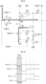
- FIG. 6 is a block diagram of a display panel which schematically illustrates an electroluminescence display according to an embodiment of the present disclosure.
- FIG. 7 is a waveform diagram explaining some of the drive characteristics of the subpixel of FIG. 6 .
- the electroluminescence display according to the first embodiment comprise an nth voltage transfer part VRD that performs an operation for transferring an externally applied voltage to subpixels so as to compensate for voltage drop in the first power supply voltage applied to the nth subpixels SP
- the term “externally” refers to the outside of the display area AA.
- the term voltage transfer part VRD is used interchangeable with the term voltage transfer transistor hereinafter, unless otherwise stated.
- the voltage transfer part VRD may represent at least one voltage transfer transistor that is located in the non-display area NA, wherein a gate electrode of the at least one voltage transfer transistor is connected to the gate driver 130 and wherein the voltage transfer transistor is configured to transfer a reference voltage to a voltage transfer node of the subpixel SP in response to a signal applied from outside the display panel 150 or a signal generated on the display panel 150.
- the nth voltage transfer part VRD is placed in the non-display area NA.
- the nth voltage transfer part VRD may be placed between the gate driver 130 disposed in the non-display area NA of the display panel and the subpixels SP disposed in the display area AA.
- the gate driver 130 comprises an nth stage STG[n] that drives the nth subpixels SP disposed in the nth scan line SCAN[n].
- the nth stage STG[n] outputs the nth emission control signal Em[n] and nth scan signal Scan[n] for driving the nth subpixels.
- the nth voltage transfer part VRD may be placed to correspond to every scan line as well as the nth scan line SCAN[n]. A plurality of nth voltage transfer parts VRD may be provided.
- the subpixels SP may be highly integrated by placing the nth voltage transfer part VRD in the non-display area NA, rather than by placing the nth voltage transfer part VRD in each of the subpixels SP disposed in the display area AA, and this allows for a high-resolution display panel.
- the nth voltage transfer part VRD acts to transfer a reference voltage applied via a reference voltage line VREF to voltage transfer nodes VDN of the nth subpixels SP during a specific period.
- the reference voltage may have a voltage level between the first power supply line EVDD and the second power supply line EVSS or a level equivalent to the first power supply voltage applied via the first power supply line EVDD.
- the nth voltage transfer part VRD comprises at least one voltage transfer transistor VT.
- the at least one voltage transfer transistor VT is turned on or off in response to an externally applied control signal or a scan signal outputted from the gate driver 130.
- the externally applied control signal may refer to, but not limited to, a control signal outputted from the timing controller or power supply part, for example.
- the nth voltage transfer part VRD is placed separately and independently from the gate driver 130.
- the nth voltage transfer part VRD may be included in the gate driver 130.
- the nth voltage transfer part VRD may be included in one of the divided gate drivers according to Fig.3 , arranged at the first side or the second side of the display panel 150.
- Placing the nth voltage transfer part VRD in the non-display area NA as in the first embodiment may offer advantages in terms of process over placing circuits for reference voltage application in the nth subpixels SP
- the advantages in terms of process are as follows. First, voltage can be transferred without placing circuits required for voltage transfer within the subpixels SP, and the number of electrodes in each subpixel SP or the number of contacts on a wire can be reduced by placing the voltage transfer circuits outside the subpixels. This heavily reduces parasitic effects that may occur when arranging it in the suppixel SP. Second, the space limitations of the subpixels can be avoided, which is advantageous in high integration and prevents a decrease in aperture ratio when making a large-screen or high-resolution display panel.
- An nth subpixel SP according to the first embodiment comprises first to seventh transistors T1 to T7, a driving transistor DT, a capacitor Cst, and an organic light-emitting diode OLED.
- the nth subpixel SP according to the first embodiment will be illustrated and described with an example in which it is implemented based on a total of 8 transistors, but the embodiment of the present specification is not limited to this example.
- the configuration and connections of the nth subpixel SP according to the first embodiment of the present disclosure will be described below. Such a configuration may be considered as a T7C1 subpixel circuit.
- the first transistor T1 has a gate connected to the nth scan line SCAN[n], a first electrode connected to the mth data line DLm, and a second electrode connected to a first electrode of the second transistor T2 and a first electrode of the driving transistor DT.
- the first transistor T1 is turned on in response to the logic-low voltage VL of the Nth scan signal Scan[n] applied via the nth scan line SCAN[n].
- a data voltage applied via the mth data line DLm is stored in the second electrode of the first transistor T1 (or between the first transistor and the second transistor).
- the second transistor T2 has a gate electrode connected to the nth emission control signal line EM[n], a first electrode connected to the second electrode of the first transistor T1, and a second electrode connected to the first power supply line EVDD and a first electrode of the seventh transistor T7.
- the second transistor T2 is turned on in response to the logic-low voltage VL of the nth emission control signal Em[n] applied via the nth emission control signal line EM[n].
- a data voltage stored in the second electrode of the first transistor T1 is transferred to one electrode of the capacitor Cst through the second transistor T2 and the seventh transistor T7.
- the third transistor T3 has a gate electrode connected to the nth scan line SCAN[n], a first electrode connected to a second electrode of the driving transistor DT, and a second electrode connected to a gate electrode of the driving transistor DT.
- the third transistor T3 is turned on in response to the logic-low voltage VL of the nth scan signal Scan[n] applied via the nth scan line SCAN[n].
- the driving transistor DT is diode-connected.
- the fourth transistor T4 has a gate electrode connected to the (n-1)th scan line SCAN[n-1], a first electrode connected to an initial line VINI, and a second electrode connected to the other electrode of the capacitor Cst, the second electrode of the third transistor T3, and the gate of the driving transistor DT.
- the fourth transistor T4 is turned on in response to the logic-low voltage VL of the (n-1)th scan signal Scan[n-1] applied via the (n-1)th scan line SCAN[n-1].
- the gate node DTG of the driving transistor DT is initialized based on the initial voltage Vini.
- the fifth transistor T5 has a gate electrode connected to the nth emission control signal line EM[n], a first electrode connected to the second electrode of the driving transistor DT, and a second electrode connected to the anode of the organic light-emitting diode OLED.
- the fifth transistor T5 is turned on in response to the logic-low voltage VL of the nth emission control signal Em[n] applied via the nth emission control signal line EM[n].
- the organic light-emitting diode OLED emits light in response to a drive current generated through the driving transistor DT.
- the sixth transistor T6 has a gate electrode connected to the nth scan line SCAN[n], a first electrode connected to the initial line VINI, and a second electrode connected to the second electrode of the driving transistor DT and the anode of the organic light-emitting diode OLED.
- the sixth transistor T6 is turned on in response to the logic-low voltage VL of the nth scan signal Scan[n] applied via the nth scan line SCAN[n].
- the anode of the organic light-emitting diode OLED is initialized based on the initial voltage Vini.
- the seventh transistor T7 has a gate electrode connected to the nth emission control signal line EM[n], a first electrode connected to the first power supply line EVDD and the second electrode of the second transistor T2, and a second electrode connected to one electrode of the capacitor Cst.
- the seventh transistor T7 is turned on in response to the logic-low voltage VL of the nth emission control signal Em[n] applied via the nth emission control signal line EM[n].
- a data voltage stored in the second electrode of the first transistor T1 is transferred to the one electrode of the capacitor Cst through the second transistor T2.
- One electrode of the capacitor Cst is connected to the second electrode of the seventh transistor T7, and the other electrode is connected to the second electrode of the fourth transistor T4.
- Anode connected to the second electrode of the seventh transistor T7 and the one electrode of the capacitor Cst is defined as a voltage transfer node VDN which transfers the reference voltage.
- the anode of the organic light-emitting diode OLED is connected to the second electrode of the fifth transistor T5, and the cathode thereof is connected to the second power supply line EVSS.
- the nth subpixel SP operates in a sequence of a first initial period INI, a sampling and second initial period SAM, a holding period HLD, and an emission period EMI.
- the first initial period INI is a period in which the gate node DTG of the driving transistor DT is initialized.
- the sampling and second initial period SAM is a period in which the threshold voltage of the driving transistor DT is sampled and the organic light-emitting diode OLED is initialized.
- the holding period HLD is a period in which a data voltage applied via the mth data line DLm is held in a particular node.
- the emission period EMI is a period in which the organic light-emitting diode OLED emits light by a drive current generated based on the data voltage.
- the Nth subpixel SP For the Nth subpixel SP according to the first embodiment, internal circuit-based compensation is done as the first initial period INI and the sampling and second initial period SAM occur while the nth emission control signal Em[n] is not applied (the logic-high voltage is maintained).
- the low-logic voltage is applied in response to the (n-1)th scan signal Scan[n-1] and the Nth scan signal Scan[n] during 1 horizontal time 1H.
- the first initial period INI and the sampling and second initial period SAM each occur during 1 horizontal time 1H.
- the fourth transistor T4 is turned on in response to the logic-low voltage VL of the (n-1)th scan signal Scan[n-1] applied via the (n-1)th scan line SCAN[n-1].
- the initial voltage Vini lower than the first power supply voltage applied via the first power supply line EVDD, is applied to the initial line VINI.
- the gate node DTG of the driving transistor DT is initial based on the initial voltage Vini.
- the first transistor T1, third transistor T3, and sixth transistor T6 are turned on in response to the logic-low voltage VL of the nth scan signal Scan[n] applied via the nth scan line SCAN[n].
- a data voltage applied via the mth data line DLm is applied to the first electrode of the driving transistor DT by the turn-on of the first transistor T1.
- the driving transistor DT is diode-connected, and the threshold voltage of the driving transistor DT is sampled.
- the data voltage applied to the first electrode of the driving transistor DT is stored in the gate node DTG.
- the organic light-emitting diode OLED is initial based on the initial voltage Vini by the turn-on of the sixth transistor T6.
- the second transistor T2, seventh transistor T7, and fifth transistor T5 are turned on in response to the logic-low voltage VL of the emission control signal Em[n] applied via the nth emission control signal line EM[n].
- the first power supply voltage applied via the first power supply line EVDD is applied to the first electrode of the driving transistor DT by the turn-on of the second transistor T2.
- the first power supply voltage applied via the first power supply line EVDD is applied to the voltage transfer node VDN, which is one electrode of the capacitor Cst, by the turn-on of the seventh transistor T7.
- the voltage of the gate node DTG of the driving transistor DT which is the other electrode of the capacitor Cst, is varied due to coupling by the amount of change from the reference voltage Vref to the first power supply voltage.
- the nth subpixel SP is supplied with the reference voltage from the nth voltage transfer part VRD during the first initial period INI and the sampling and second initial period SAM so that voltage drops in the first power supply voltage are taken into consideration.
- Ioled is determined by the difference between the reference voltage and the data voltage. From the equation, it can be seen that, for the nth subpixel SP according to the first embodiment, voltage drops in the first power supply voltage applied via the first power supply line EVDD are compensated for by the reference voltage applied during the first initial period INI and the sampling and second initial period SAM.
- the nth voltage transfer part VRD consists of two voltage transfer transistors.
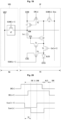
- FIG. 8 is a view showing in more detail the configuration of an nth voltage transfer part according to the first embodiment of the present disclosure.
- FIGs. 9 to 16 are views explaining in more detail the driving method according to the configuration of FIG. 8 .
- the nth voltage transfer part VT comprises a first voltage transfer transistor VTa and a second voltage transfer transistor Vtb.
- the first voltage transfer transistor VTa is turned on or off in response to the (n-1)th scan signal applied via the (n-1)th scan line SCAN[n-1].
- the second voltage transfer transistor Vtb is turned on or off in response to the nth scan signal applied through the nth scan line SCAN[n],
- the first voltage transfer transistor VTa has a gate connected to the (n-1)th scan line SCAN[n-1], a first electrode connected to the reference voltage line VREF, and a second electrode connected to the second electrode of the seventh transistor T7 and the voltage transfer node VDN, which is one electrode of the capacitor Cst.
- the second voltage transfer transistor VTb has a gate connected to the nth scan line SCAN[n], a first electrode connected to the reference voltage line VREF, and a second electrode connected to the second electrode of the seventh transistor T7 and the voltage transfer node VDN, which is one electrode of the capacitor Cst. That is, the gates of the first voltage transfer transistor VTa and the second voltage transfer transistor VTb are connected to different scan lines, and the first electrodes thereof are connected to each other and the second electrodes thereof are connected to each other.
- the driving method according to the first embodiment will be described below in conjunction with the nth voltage transfer part VT and the nth subpixel SP.
- the transistors marked by a slash are turned-off transistors, and the other transistors are tumed-on transistors.
- FIGs. 9 and 10 are views showing an operation during a first initial period and the resulting drive waveforms according to the configuration of FIG. 8 .
- the first voltage transfer transistor VTa is turned on in response to the logic-low voltage VL of the (n-1)th scan signal Scan[n-1] applied via the (n-1)th scan line SCAN[n-1].
- the reference voltage transferred via the reference voltage line VREF is applied to the nth subpixels via the turned-on first voltage transfer transistor VTa.
- the reference voltage is stored at one electrode of the capacitor Cst.
- the fourth transistor T4 is turned on in response to the logic-low voltage VL of the (n-1)th scan signal Scan[n-1] applied via the (n-1)th scan line SCAN[n-1].
- the initial voltage lower than the first power supply voltage applied via the first power supply line EVDD, is applied to the initial line VINI.
- the gate node DTG of the driving transistor DT is initialized based on the initial voltage Vini (or residual voltage is released).
- FIGs. 11 and 12 are views showing an operation during a sampling and second initial period and the resulting drive waveforms according to the configuration of FIG. 8 .
- the second voltage transfer transistor VTb is turned on in response to the logic-low voltage VL of the nth scan signal Scan[n] applied via the nth scan line SCAN[n].
- the reference voltage transferred via the reference voltage line VREF is applied to the nth subpixels via the tumed-on second voltage transfer transistor VTb.
- the reference voltage is continuously stored at one electrode of the capacitor Cst.
- the first transistor T1, third transistor T3, and sixth transistor T6 are turned on in response to the logic-low voltage VL of the nth scan signal Scan[n] applied via the nth scan line SCAN[n].
- a data voltage applied via the mth data line DLm is applied to the first electrode of the driving transistor DT by the turn-on of the first transistor T1.
- the driving transistor DT is diode-connected by the turn-on of the third transistor T3.
- the threshold voltage of the driving transistor DT is sampled by the turn-on of the third transistor T3.
- the data voltage applied to the first electrode of the driving transistor DT is stored in the gate node DTG via the third transistor T3.
- the organic light-emitting diode OLED is initialized based on the initial voltage Vini by the turn-on of the sixth transistor T6.
- FIGs. 13 and 14 are views showing an operation during a holding period and the resulting drive waveforms according to the configuration of FIG. 8 .
- the first voltage transfer transistor VTa is turned off in response to the logic-high voltage VH of the (n-1)th scan signal Scan[n-1] applied via the (n-1)th scan line SCAN[n-1].
- the second voltage transfer transistor VTb is turned off in response to the logic-high voltage VH of the nth scan signal Scan[n] applied via the nth scan line SCAN[n].
- the first to seventh transistors T1 to T7 are turned off in response to the logic-high voltage VH of the (n-1)th scan signal Scan[n-1], nth scan signal Scan[n], and nth emission control signal Em[n].
- the capacitor Cst stores and holds a data voltage based on the voltage difference between the two ends.
- FIGs. 15 and 16 are views showing an operation during an emission period and the resulting drive waveforms according to the configuration of FIG. 8 .
- the first voltage transfer transistor VTa and the second voltage transfer transistor VTb are kept turned off, as is during the holding period HLD.
- the second transistor T2, fifth transistor T5, and seventh transistor T7 are turned on in response to the logic-low voltage VL of the nth emission control signal Em[n].
- the driving transistor DT are turned on while generating a drive current based on a data voltage obtained by threshold voltage compensation.
- the first embodiment can prevent or solve picture quality issues such as vertical luminance non-uniformity or crosstalk on the display panel since defect issues caused by voltage drop in the first power supply voltage can be prevented or solved.
- the first embodiment can reduce the number of electrodes in each subpixel or the number of contacts on a wire by placing circuits for transferring reference voltage to the subpixels, and also can offer advantages in high integration and therefore prevents a decrease in aperture ratio when making a large-screen or high-resolution display panel.
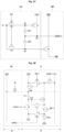
- FIG. 17 is a diagram of the configuration of a display panel which schematically explains an electroluminescence display according to a second embodiment of the present disclosure.
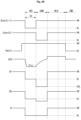
- FIG. 18 is a waveform diagram explaining some of the drive characteristics of the subpixel circuit of FIG. 17 .
- the second embodiment of the present disclosure is a modification of the first embodiment, so redundancies between the first and second embodiments will be omitted or described briefly.
- the electroluminescence display according to the second embodiment comprise an Nth voltage transfer part VRD that performs an operation for transferring an externally applied voltage to subpixels so as to compensate for voltage drop in the first power supply voltage applied to the nth subpixels SP.
- the term “externally” refers to the outside of the display area AA.
- the nth voltage transfer part VRD is placed in the non-display area NA.
- the nth voltage transfer part VRD acts to transfer a reference voltage applied via a reference voltage line VREF to voltage transfer nodes VDN of the nth subpixels SP during a specific period.
- the nth voltage transfer part VRD comprises one voltage transfer transistor VT.
- the voltage transfer transistor VT has a gate electrode connected to the nth scan line SCAN[n], a first electrode connected to the reference voltage line VREF, and a second electrode connected to the second electrode of the seventh transistor T7 and one electrode of the capacitor Cst.
- the voltage transfer transistor VT is turned on or off in response to the nth scan signal Scan[n] applied via the nth scan line SCAN[n],
- the nth voltage transfer part VRD may comprise a single voltage transfer transistor VT by configuring the (n-1)th scan line SCAN[n-1] and the nth scan line SCAN[n] in such a way that their logic-low voltage parts overlap.
- the nth voltage transfer part VRD can be kept turned on for at least 2 horizontal times, without changing from the turned-off state to the tumed-on state for a specific period of time, since the previous scan signal and the current scan signal overlap when applied.
- power supply can be prevented from being cut off when the reference voltage is transferred, or the nodes can be prevented from electrically floating.
- the nth voltage transfer part VRD comprises a single voltage transfer transistor VT, thereby simplifying the circuits enough to further reduce the non-display area (or bezel area) of the display panel.
- scan signals for 2 horizontal times may have a compensation period only when the pulses overlap.
- applying the reference voltage to the subpixels during the initial period INI may be necessary depending on whether the scan signals overlap or not.
- An nth subpixel SP according to the second embodiment comprises first to seventh transistors T1 to T7, a driving transistor DT, a capacitor Cst, and an organic light-emitting diode OLED.
- the driving transistor DT and the organic light-emitting diode OLED are simultaneously initial, unlike the first embodiment.
- the configuration and connections of the nth subpixel SP according to the second embodiment of the present disclosure will be described below.
- the first transistor T1 has a gate connected to the nth scan line SCAN[n], a first electrode connected to the mth data line DLm, and a second electrode connected to a first electrode of the second transistor T2 and a first electrode of the driving transistor DT.
- the first transistor T1 is turned on in response to the logic-low voltage VL of the nth scan signal Scan[n] applied via the nth scan line SCAN[n].
- a data voltage applied via the mth data line DLm is stored in the second electrode of the first transistor T1.
- the second transistor T2 has a gate connected to the nth emission control signal line EM[n], a first electrode connected to the second electrode of the first transistor T1, and a second electrode connected to the first power supply line EVDD and a first electrode of the seventh transistor T7.
- the second transistor T2 is turned on in response to the logic-low voltage VL of the nth emission control signal Em[n] applied via the nth emission control signal line EM[n].
- a data voltage stored in the second electrode of the first transistor T1 is transferred to one electrode of the capacitor Cst through the seventh transistor T7.
- the third transistor T3 has a gate connected to the nth scan line SCAN[n], a first electrode connected to a second electrode of the driving transistor DT, and a second electrode connected to a gate of the driving transistor DT.
- the third transistor T3 is turned on in response to the logic-low voltage VL of the nth scan signal Scan[n] applied via the nth scan line SCAN[n].
- the driving transistor DT is diode-connected.
- the fourth transistor T4 has a gate connected to the (n-1)th scan line SCAN[n-1], a first electrode connected to an initial line VINI, and a second electrode connected to the other electrode of the capacitor Cst, the second electrode of the third transistor T3, and the gate of the driving transistor DT.
- the fourth transistor T4 is turned on in response to the logic-low voltage VL of the (n-1)th scan signal Scan[n-1] applied via the (n-1)th scan line SCAN[n-1].
- the gate node DTG of the driving transistor DT is initial based on the initial voltage Vini.
- the fifth transistor T5 has a gate electrode connected to the nth emission control signal line EM[n], a first electrode connected to the second electrode of the driving transistor DT, and a second electrode connected to the anode of the organic light-emitting diode OLED.
- the fifth transistor T5 is turned on in response to the logic-low voltage VL of the nth emission control signal Em[n] applied via the nth emission control signal line EM[n].
- the organic light-emitting diode OLED emits light in response to a drive current generated through the driving transistor DT.
- the sixth transistor T6 has a gate electrode connected to the (n-1)th scan line SCAN[n-1], a first electrode connected to the initial line VINI, and a second electrode connected to the second electrode of the driving transistor DT and the anode of the organic light-emitting diode OLED.
- the sixth transistor T6 is turned on in response to the logic-low voltage of the (n-1)th scan signal Scan[n-1] applied via the (n-1)th scan line SCAN[n-1].
- the anode of the organic light-emitting diode OLED is initialized based on the initial voltage Vini.
- the seventh transistor T7 has a gate electrode connected to the nth emission control signal line EM[n], a first electrode connected to the first power supply line EVDD and the second electrode of the second transistor T2, and a second electrode connected to one electrode of the capacitor Cst.
- the seventh transistor T7 is turned on in response to the logic-low voltage VL of the nth emission control signal Em[n] applied via the nth emission control signal line EM[n].
- a data voltage stored in the second electrode of the first transistor T1 is transferred to the one electrode of the capacitor Cst through the second transistor T2.
- One electrode of the capacitor Cst is connected to the second electrode of the seventh transistor T7, and the other electrode is connected to the second electrode of the fourth transistor T4.
- the anode of the organic light-emitting diode OLED is connected to the second electrode of the fifth transistor T5, and the cathode thereof is connected to the second power supply line EVSS.
- the Nth subpixel SP operates in a sequence of an initial period INI, a sampling period SAM, a holding period HLD, and an emission period EMI.
- the initial period INI is a period in which the gate node DTG of the driving transistor DT and the organic light-emitting diode OLED are simultaneously initialized.
- the sampling period SAM is a period in which the threshold voltage of the driving transistor DT is sampled.
- the holding period HLD is a period in which a data voltage applied via the mth data line DLm is held in a particular node.
- the emission period EMI is a period in which the organic light-emitting diode OLED emits light by a drive current generated based on the data voltage.
- nth subpixel SP For the nth subpixel SP according to the second embodiment, internal circuit-based compensation is done as the initial period INI and the sampling period SAM occur while the nth emission control signal Em[n] is not applied (the logic-high voltage is maintained). The operating characteristics during these periods will be described below in brief.
- the low-logic voltage is applied in response to the (n-1)th scan signal Scan[n-1] and the nth scan signal Scan[n] during 2 horizontal times 2H, and the two signals overlap during 1 horizontal time 1H.
- the fourth transistor T4 and the sixth transistor T6 are simultaneously turned on in response to the logic-low voltage VL of the (n-1)th scan signal Scan[n-1] applied via the (n-1)th scan line SCAN[n-1].
- the initial voltage lower than the first power supply voltage applied via the first power supply line EVDD, is applied to the initial line VINI.
- the gate node DTG of the driving transistor DT and the organic light-emitting diode OLED are initialized based on the initial voltage.
- the first transistor T1 and the third transistor T3 are turned on in response to the logic-low voltage VL of the nth scan signal Scan[n] applied via the Nth scan line SCAN[n].
- a data voltage applied via the mth data line DLm is transferred to the nth subpixel SP by the turn-on of the first transistor T1.
- the driving transistor DT is diode-connected.
- the threshold voltage of the driving transistor DT is sampled.
- the nth subpixel SP according to the second embodiment is supplied with the reference voltage from the nth voltage transfer part VRD during the initial period INI and the sampling period SAM so that voltage drops in the first power supply voltage are taken into consideration. Accordingly, for the nth subpixel according to the second embodiment as well, voltage drops in the first power supply voltage applied via the first power supply line EVDD may be compensated for by the reference voltage.
- the second embodiment may offer the same benefit as the first embodiment since the nth voltage transfer part VRD is capable of applying the reference voltage during the initial period INI and the sampling period SAM. Moreover, in the second embodiment, power supply can be prevented from being cut off when the reference voltage is transferred, or the nodes can be prevented from electrically floating.
- the nth voltage transfer part VRD comprises a single voltage transfer transistor VT, thereby simplifying the circuits enough to further reduce the non-display area (or bezel area) of the display panel.
- FIG. 19 is a diagram of the configuration of a display panel which schematically explains an electroluminescence display according to a third embodiment of the present disclosure.
- FIG. 20 is a waveform diagram explaining some of the drive characteristics of the subpixel circuit of FIG. 19 .
- the third embodiment of the present disclosure is a modification of the first and second embodiments, so redundancies between the third embodiment and the first and second embodiments will be omitted or described briefly.
- the electroluminescence display according to the third embodiment comprise an nth voltage transfer part VRD that performs an operation for transferring an externally applied voltage to subpixels so as to compensate for voltage drop in the first power supply voltage applied to the nth subpixels SP
- the term “externally” refers to the outside of the display area AA.
- the nth voltage transfer part VRD is placed in the non-display area NA.
- the nth voltage transfer part VRD acts to transfer a reference voltage applied via a reference voltage line VREF to voltage transfer nodes VDN of the nth subpixels SP during a specific period.
- the nth voltage transfer part VRD comprises one voltage transfer transistor VT.
- the voltage transfer transistor VT has a gate electrode connected to the (n-2)th scan line SCAN[n-1], a first electrode connected to the reference voltage line VREF, and a second electrode connected to the second electrode of the seventh transistor T7 and the voltage transfer node VDN, which is one electrode of the capacitor Cst.
- the voltage transfer transistor VT is turned on or off in response to the (n-1)th scan signal Scan[n-1] applied via the (n-1)th scan line SCAN[n-1].
- the nth voltage transfer part VRD may comprise a single voltage transfer transistor VT by configuring the (n-1)th scan line SCAN[n-1] and the nth scan line SCAN[n] in such a way that their logic-low voltage parts overlap.
- An nth subpixel SP comprises first to third transistors T1 to T3, fifth to seventh transistors T5 to T7, a driving transistor DT, a capacitor Cst, and an organic light-emitting diode OLED.
- the nth subpixel SP according to the third embodiment does not comprise the fourth transistor T4, as opposed to that of the second embodiment.
- the driving transistor DT is diode-connected and, at the same time, the organic light-emitting diode OLED is initialized. Specifically, in response to the (n-1)th scan signal Scan[n-1], the driving transistor DT is diode-connected, and the organic light-emitting diode OLED is initialized. Moreover, the fifth transistor T5 is turned on in response to the (n+1)th emission control signal Em[n+1] and transfers a drive current generated through the driving transistor DT to the organic light-emitting diode OLED.
- Em[n+1] emission control signal
- the first transistor T1 has a gate connected to the nth scan line SCAN[n], a first electrode connected to the mth data line DLm, and a second electrode connected to a first electrode of the second transistor T2 and a first electrode of the driving transistor DT.
- the first transistor T1 is turned on in response to the logic-low voltage VL of the nth scan signal Scan[n] applied via the nth scan line SCAN[n].
- a data voltage applied via the mth data line DLm is stored in the second electrode of the first transistor T1.
- the second transistor T2 has a gate electrode connected to the nth emission control signal line EM[n], a first electrode connected to the second electrode of the first transistor T1, and a second electrode connected to the first power supply line EVDD and a first electrode of the seventh transistor T7.
- the second transistor T2 is turned on in response to the logic-low voltage VL of the nth emission control signal Em[n] applied via the nth emission control signal line EM[n].
- a data voltage stored in the second electrode of the first transistor T1 is transferred to one electrode of the capacitor Cst through the seventh transistor T7.
- the third transistor T3 has a gate electrode connected to the (n-1)th scan line SCAN[n-1], a first electrode connected to a second electrode of the driving transistor DT, and a second electrode connected to a gate electrode of the driving transistor DT.
- the third transistor T3 is turned on in response to the logic-low voltage VL of the (n-1)th scan signal Scan[n-1] applied via the (n-1)th scan line SCAN[n-1].
- the driving transistor DT is diode-connected.
- the fifth transistor T5 has a gate electrode connected to the (n+1)th emission control signal line EM[n+1], a first electrode connected to the second electrode of the driving transistor DT, and a second electrode connected to the anode of the organic light-emitting diode OLED.
- the fifth transistor T5 is turned on in response to the logic-low voltage VL of the (n+1)th emission control signal Em[n+1] applied via the (n+1)th emission control signal line EM[n+1].
- the organic light-emitting diode OLED emits light in response to a drive current generated through the driving transistor DT.
- the sixth transistor T6 has a gate electrode connected to the (n-1)th scan line SCAN[n-1], a first electrode connected to the initial line VINI, and a second electrode connected to the second electrode of the driving transistor DT and the anode of the organic light-emitting diode OLED.
- the sixth transistor T6 is turned on in response to the logic-low voltage of the (n-1)th scan signal Scan[n-1] applied via the (n-1)th scan line SCAN[n-1].
- the anode of the organic light-emitting diode OLED is initialized based on the initial voltage Vini.
- the seventh transistor T7 has a gate electrode connected to the nth emission control signal line EM[n], a first electrode connected to the first power supply line EVDD and the second electrode of the second transistor T2, and a second electrode connected to one electrode of the capacitor Cst.
- the seventh transistor T7 is turned on in response to the logic-low voltage VL of the nth emission control signal Em[n] applied via the nth emission control signal line EM[n].
- a data voltage stored in the second electrode of the first transistor T1 is transferred to the one electrode of the capacitor Cst through the second transistor T2.
- One electrode of the capacitor Cst is connected to the second electrode of the seventh transistor T7, and the other electrode is connected to the second electrode of the fourth transistor T4.
- a node provided at the second electrode of the seventh transistor T7 and the one electrode of the capacitor Cst is defined as a voltage transfer node VDN which transfers the reference voltage.
- the anode of the organic light-emitting diode OLED is connected to the second electrode of the fifth transistor T5, and the cathode thereof is connected to the second power supply line EVSS.
- the Nth subpixel SP operates in a sequence of an initial and sampling period INI & SAM, a holding period HLD, and an emission period EMI.
- the initial and sampling period INI and SAM is a period in which the organic light-emitting diode OLED is initialized and the threshold voltage of the driving transistor DT is sampled.
- the holding period HLD is a period in which a data voltage applied via the mth data line DLm is held in a particular node.
- the emission period EMI is a period in which the organic light-emitting diode OLED emits light by a drive current generated based on the data voltage. The emission period EMI occurs not by the nth emission signal Em[n] but by the (n+1)th emission signal Em[n+1],
- the emission control signal may be applied longer than 3 horizontal times, e.g., up to 4 horizontal times, and then emit light based on the next emission control signal. That is, if the nth subpixel SP, which is at the current stage, emits light based on the (n+1)th emission control signal Em[n+1], which is the next emission control signal, this means that a signal for forming the emission period EMI may be selected freely.
- This method has the advantage of avoiding space limitations when designing or changing the layout of subpixels (because the degree of freedom for the arrangement of signal lines is high).
- nth subpixel SP For the nth subpixel SP according to the third embodiment, internal circuit-based compensation is done as the initial and sampling period INI & SAM occurs while the nth emission control signal Em[n] is not applied (the logic-high voltage is maintained). The operating characteristics during these periods will be described below in brief.
- the low-logic voltage is applied in response to the (n-1)th scan signal Scan[n-1] and the nth scan signal Scan[n] during 2 horizontal times 2H, and the two signals overlap during 1 horizontal time 1H.
- the third transistor T3 and the sixth transistor T6 are simultaneously turned on in response to the logic-low voltage VL of the (n-1)th scan signal Scan[n-1] applied via the (n-1)th scan line SCAN[n-1].
- the threshold voltage of the driving transistor DT is sampled, and the organic light-emitting diode OLED is initialized based on the initial voltage.
- the Nth subpixel SP according to the third embodiment is supplied with the reference voltage from the Nth voltage transfer part VRD during the initial and sampling period INI & SAM so that voltage drops in the first power supply voltage are taken into consideration. Accordingly, for the nth subpixel according to the third embodiment as well, voltage drops in the first power supply voltage applied via the first power supply line EVDD may be compensated for by the reference voltage applied during the initial and sampling period INI & SAM.
- the second embodiment may offer the same benefit as the first embodiment since the nth voltage transfer part VRD is capable of applying the reference voltage during the initial and sampling period INI & SAM.
- power supply can be prevented from being cut off when the reference voltage is transferred, or the nodes can be prevented from electrically floating.
- the nth voltage transfer part VRD comprises a single voltage transfer transistor VT, thereby simplifying the circuits enough to further reduce the non-display area (or bezel area) of the display panel.
- the third embodiment can overcome space limitations when designing or changing the layout of subpixels because the degree of freedom for the arrangement of signal lines is high.
- the present specification can solve or improve picture quality issues such as vertical luminance non-uniformity or crosstalk on the display panel by compensating for time-varying characteristics, with voltage drops on voltage supply lines taken into consideration. Moreover, the present specification can reduce the number of electrodes in each subpixel or the number of contacts on a wire by placing circuits for transferring reference voltage to the subpixels, and also can offer advantages in high integration, thereby preventing a decrease in aperture ratio when making a large-screen or high-resolution display panel.
- FIG. 21 is a circuit diagram showing the configuration of a voltage transfer part and a gate driver according to a first modification of one of the first to third embodiments of the present specification.
- the nth voltage transfer part VRD may comprise a single voltage transfer transistor VT.
- the voltage transfer transistor VT may be controlled by being connected to a component of the gate driver 130.
- the gate driver illustrated in FIG. 21 illustrates only some of the components for explaining the connections of the voltage transfer transistor VT.
- the gate driver 130 comprises a pull-up transistor Tu, a first boosting capacitor CQ1, and a first shut-off transistor Tb1.
- the pull-up transistor Tu outputs a gate-on voltage to the nth scan line SCAN[n] via a scan output node SO. If a transistor connected to the nth scan line SCAN[n] is a p-type transistor, the gate-on voltage is the logic-low voltage, and if a transistor connected to the nth scan line SCAN[n] is an n-type transistor, the gate-on voltage is the logic-high voltage.
- the pull-up transistor Tu has a Q1 node Q1, a first electrode connected to a clock signal line CLKL providing clock signals, and a second electrode connected to the scan output node SO.
- the pull-up transistor Tu is turned on in response to the logic-low voltage input into the Q1 node Q1 and applies clock signals to the scan output node SO.
- One electrode of the first boosting capacitor CQ1 is connected to the gate of the pull-up transistor Tu, and the other electrode is connected to the second electrode of the pull-up transistor Tu and the scan output node SO.
- the first boosting capacitor CQ1 allows the pull-up transistor Tu to stably apply the gate-on voltage to the scan output node SO by boosting the gate of the pull-up transistor Tu when the pull-up transistor Tu is turned on.
- the first shut-off transistor Tb1 has a gate connected to a logic-low voltage line VLL via which the logic-low voltage is applied, a first electrode connected to the Q1 node Q1, and a second electrode connected to the Q node Q.
- the first shut-off transistor Tb1 is always kept turned on since the logic-low voltage is applied to its gate, thereby preventing voltage changes at the Q1 node Q1 from affecting other transistors connected to the Q node Q.
- the voltage transfer transistor VT has a gate connected to the Q1 node Q1, a first electrode connected to the reference voltage line VREF, and a second electrode connected to the voltage transfer node VDN.
- the voltage transfer transistor VT is turned on in response to the logic-low voltage applied to the Q1 node Q1.
- the reference voltage is applied to the voltage transfer node VDN while the pull-up transistor Tu is turned on by the logic-low voltage applied to the Q node Q.
- the reference voltage is applied to the voltage transfer node VDN while the logic-low voltage is applied to the nth scan line SCAN[n],
- FIG. 22 is a circuit diagram showing a voltage transfer part and a subpixel according to a first example of the present disclosure.
- the nth voltage transfer part VRD may comprise a voltage transfer transistor VT, as illustrated in FIG. 6 .
- FIG. 22 illustrates the connections between the voltage transfer part VRD and the subpixel SP Moreover, the components of the subpixels SP are identical to the components of the subpixel SP explained in FIG. 6 may be omitted or explained briefly.
- the voltage transfer transistor VT has a gate connected to the Q1 node Q1, a first electrode connected to the reference voltage line VREF, and a second electrode connected to the voltage transfer node VDN.
- the voltage transfer transistor VT is turned on in response to the logic-low voltage applied to the Q1 node Q1 and applies the reference voltage to the voltage transfer node VDN.
- FIGs. 23A to 26B are views showing operations and waveforms of FIG. 22 .
- FIG. 23A is a view showing an operation during a first initial period of FIG. 22 .
- FIG. 23B is a waveform diagram showing the operation of FIG. 23A .
- FIG. 24A is a view showing an operation during a sampling and second period of FIG. 22 .
- FIG. 24B is a waveform diagram showing the operation of FIG. 24A .
- FIG. 25A is a view showing an operation during a holding period of FIG. 22 .
- FIG. 25B is a waveform diagram showing the operation of FIG. 25A .
- FIG. 26A is a view showing an operation during an emission period of FIG. 22 .
- FIG. 26B is a waveform diagram showing the operation of FIG. 26A .
- the fourth transistor T4 is turned on in response to the logic-low voltage VL applied via the (n-1)th scan line SCAN[n-1] during the first initial period INI. Since the initial voltage Vini is applied to the gate DTG of the driving transistor DT through the tumed-on fourth transistor T4, the gate node DTG of the driving transistor DT is initialized to the initial voltage Vini. Moreover, the voltage transfer transistor VT is turned on in response to the logic-low voltage VL applied to the Q1 node Q1 during the first initial period INI. The reference voltage is applied to the voltage transfer node VDN through the tumed-on voltage transfer transistor VT.
- the first transistor T1, third transistor T3, driving transistor DT, and sixth transistor T6 are turned on in response to the logic-low voltage VL applied via the nth scan line SCAN[n] during the sampling and second initial period SAM.
- the gate and drain electrode of the driving transistor are connected together by the turned-on third transistor T3, and a data voltage Vdata is applied to the source electrode of the driving transistor DT through the tumed-on first transistor T1, thereby turning on the driving transistor DT.
- the voltage of the gate node DTG of the driving transistor DT rises up to the difference between the data voltage Vdata and the threshold voltage Vth of the driving transistor DT.
- the Q1 node Q1 is boosted during the sampling and second initial period SAM to apply the logic-low voltage through the nth scan line SCAN[n], and therefore the voltage transfer transistor VT is turned on to apply the reference voltage to the voltage transfer node VDN.
- the boosted voltage of the Q1 node Q1 is lower than the logic-low voltage VL and higher than 2VL, which is twice as high as the logic-low voltage.
- between the data voltage applied to the other electrode of the capacitor Cst are stored as a capacitance.
- the sixth transistor T6 is turned on during the sampling and second initial period SAM to initial the anode of the organic light-emitting diode OLED to the initial voltage Vini.
- the voltage transfer transistor is turned on during the first initial period in response to the logic-low voltage of the (n-1)th scan signal for driving the (N-1)th subpixels of the (n-1)th scan line and during the sampling and second initial period in response to the nth scan signal for driving the nth subpixels of the Nth scan line, thereby applying the reference voltage to the subpixels.
- the subpixels applied with the reference voltage supplies the organic light-emitting diodes with a drive current not affected by the first power supply voltage, thereby improving the problem of the picture quality of the electroluminescence display.
- the logic-high voltage VH is applied to the Q1 node during the holding period HLD to thereby turn off the voltage transfer transistor VT.
- the (n-1)th scan signal Scan[n-1] and the nth scan signal Scan[n] are the logic-high voltage VH, which causes all transistors constituting the subpixel to be turned off.
- the holding period HLD varies with the cycle of clock signals from an emission driver outputting the nth emission control signal Em[n] and the cycle of clock signals from the gate driver outputting the Nth scan signal Scan[n].
- the holding period HLD may be longer than 1 horizontal time 1H.
- the capacitor Cst stores and maintains a data voltage based on the voltage difference between the two ends.
- the voltage of the gate node DTG of the driving transistor DT may be slightly varied by a parasitic capacitor of the third transistor T3.
- the second transistor T2, seventh transistor T7, and fifth transistor T5 are turned on in response to the logic-low voltage VL of the nth emission control signal Em[n] applied via the nth emission control signal line EM[n] during the emission period EMI.
- the first power supply voltage VDD is applied to one electrode of the capacitor Cst through the tumed-on seventh transistor T7.
- the first power supply voltage VDD is applied to the first electrode of the driving transistor DT through the turned-on second transistor T2, and the fifth transistor T5 is turned on, thereby turning on the driving transistor DT.
- the turned-on driving transistor DT provides a drive current to the anode of the organic light-emitting diode, thereby causing the organic light-emitting diode to emit light.
- the voltage applied to one electrode of the capacitor Cst is varied, so the voltage of the other electrode of the capacitor Cst is also varied due to coupling.
- the drive current provided to the anode of the organic light-emitting diode OLED is the same as represented by the equation mentioned with respect to FIG. 3 .
- the voltage transfer transistor VT for applying the reference voltage may be disposed at one electrode of the capacitor Cst. Therefore, a drive circuit for compensating for time-varying characteristics (or variation with time) may be implemented, with drops in power-supply voltage taken into consideration, and this can solve picture quality problems such as vertical luminance non-uniformity or crosstalk on the display panel.
- FIG. 27 is a circuit diagram showing the configuration of a voltage transfer part and a gate driver according to a second modification of one of the first to third embodiments and first example of the present disclosure.
- FIG. 27 shows a modification of the connections of the voltage transfer part due to an alteration to the configuration of the gate driver 130 of FIG. 21 , so any redundancies will be omitted or explained briefly.
- the nth voltage transfer part VRD may comprise a single voltage transfer transistor VT.
- the voltage transfer transistor VT may be controlled by being connected to a component of the gate driver 130.
- the gate driver illustrated in FIG. 27 illustrates only some of the components for explaining the connections of the voltage transfer transistor VT.
- the gate driver 130 comprises a pull-up transistor Tu, a first boosting capacitor CQ1, a second boosting capacitor CQ2, a first shut-off transistor Tb1, and a second shut-off transistor Tb2.
- the pull-up transistor Tu outputs a gate-on voltage to the nth scan line SCAN[n] via a scan output node SO.
- the pull-up transistor Tu has a Q1 node Q1, a first electrode connected to a clock signal line CLKL providing clock signals, and a second electrode connected to the scan output node SO.
- the pull-up transistor Tu is turned on in response to the logic-low voltage input into the Q1 node Q1 and applies clock signals to the scan output node SO.
- One electrode of the first boosting capacitor CQ1 is connected to the gate of the pull-up transistor Tu, and the other electrode is connected to the second electrode of the pull-up transistor Tu and the scan output node SO.
- the first boosting capacitor CQ1 allows the pull-up transistor Tu to stably apply the gate-on voltage to the scan output node SO by boosting the gate electrode of the pull-up transistor Tu when the pull-up transistor Tu is turned on.
- One electrode of the second boosting capacitor CQ2 is connected to the other electrode of the first bosting capacitor CQ1, and the other electrode is connected to a Q2 node Q2 and the gate of the voltage transfer transistor VT.
- the gate of the voltage transfer transistor VT is connected to the Q1 node Q1, and the Q1 node Q1 forms a parasitic capacitance as well as the capacitance caused by the first boosting capacitor CQ1. Due to the parasitic capacitance caused by the voltage transfer transistor VT, the boosting efficiency of the Q1 node Q1 may be decreased.
- the gate of the voltage transfer transistor VT may be separated from the Q1 node Q by using the second boosting capacitor CQ2 in the gate driver 130, thereby preventing a decrease in the boosting efficiency of the Q1 node Q1.
- the first shut-off transistor Tb1 has a gate connected to a logic-low voltage line VLL via which the logic-low voltage is applied, a first electrode connected to the Q1 node Q1, and a second electrode connected to the Q node Q.
- the first shut-off transistor Tb1 is always kept turned on since the logic-low voltage is applied to its gate, thereby preventing voltage changes at the Q1 node Q1 from affecting other transistors connected to the Q node Q.
- the second shut-off transistor Tb2 has a gate connected to the logic-low voltage line VLL via which the logic-low voltage is applied, a first electrode connected to the Q2 node Q2, and a second electrode connected to the Q node Q.
- the second shut-off transistor Tb2 is always kept turned on since the logic-low voltage is applied to its gate, thereby preventing voltage changes at the Q2 node Q2 from affecting other transistors connected to the Q node Q.
- the second shut-off transistor Tb2 separates the gate of the voltage transfer transistor VT form the Q1 node Q1, along with the second boosting capacitor CQ2.
- the voltage transfer transistor VT has a gate connected to the Q2 node Q2, a first electrode connected to the reference voltage line VREF, and a second electrode connected to the voltage transfer node VDN.
- the voltage transfer transistor VT is turned on in response to the logic-low voltage applied to the Q2 node Q2.
- the reference voltage is applied to the voltage transfer node VDN while the pull-up transistor Tu is turned on by the logic-low voltage applied to the Q node Q.
- the reference voltage is applied to the voltage transfer node VDN while the logic-low voltage is applied to the nth scan line SCAN[n],
- FIG. 28 is a circuit diagram showing a voltage transfer part and a subpixel according to a second example of the present disclosure.
- the nth voltage transfer part VRD may comprise a voltage transfer transistor VT, as illustrated in FIG. 27.
- FIG. 28 illustrates the connections between the voltage transfer part VRD and the subpixel SP Moreover, the components of the subpixels SP are identical to the components of the subpixel SP explained in FIG. 6 may be omitted or explained briefly.
- the voltage transfer transistor VT has a gate connected to the Q2 node Q2, a first electrode connected to the reference voltage line VREF, and a second electrode connected to the voltage transfer node VDN.
- the voltage transfer transistor VT is turned on in response to the logic-low voltage applied to the Q2 node Q2 and applies the reference voltage to the voltage transfer node VDN.
- FIG. 29 is a view showing an operation of FIG. 28 .
- the nth subpixel SP operates in a sequence of a first initial period INI, a sampling and second initial period SAM, a holding period HLD, and an emission period EMI.
- the operations of the subpixel SP in the respective phases are identical to those shown in FIGs. 23A , 24A , 25A , and 26A according to the second example of the present disclosure, so any redundancies will be omitted or explained briefly.
- the gate node DTG of the driving transistor DT is initial to the initial voltage Vini by the logic-low voltage VL of the (n-1)th scan signal Scan[n-1]. Also, the logic-low voltage VL is applied to the Q1 node Q1 and the Q2 node Q2 in response to the logic-low voltage VL applied to the Q node Q.
- the voltage applied to the gate node DTG of the driving transistor DT by the logic-low voltage VL of the nth scan signal Scan[n] rises up to the difference between the data voltage and the threshold voltage of the driving transistor DT.
- the Q1 node Q1 is boosted by the first boosting capacitor CQ1, and the voltage of the Q1 node Q1 drops to 2VL which is lower than the logic-low voltage VL, thereby properly outputting the logic-low voltage VL to the nth scan line SCAN[n]. Accordingly, the efficiency of the gate driver 130 can be improved.
- the gate of the voltage transfer transistor VT is connected to the Q2 node Q2, thereby keeping the voltage of the Q2 node Q2 from dropping as much as the voltage at the Q1 node Q1 drops due to the parasitic capacitance of the voltage transfer transistor VT.
- the nth scan signal Scan[n], Q node Q, Q1 node Q1, and Q2 node may be switched to the logic-high voltage VH, and the (n-1)th scan signal Scan[n-1] and the nth emission control signal Em[n] may be kept at the logic-high voltage VH.
- the holding period HLD may be maintained for 1 horizontal time 1H or longer.
- the capacitor Cst stores and maintains a data voltage based on the voltage difference between the two ends.
- the voltage of the gate node DTG of the driving transistor DT may be slightly varied by a parasitic capacitor of the third transistor T3.
- the nth emission control signal Em[n] is switched to the logic-low voltage VL, and the driving transistor DT is turned on.
- the tumed-on driving transistor DT provides a drive current to the anode of the organic light-emitting diode OLED, thereby causing the organic light-emitting diode OLED to emit light.
- the drive current provided to the anode of the organic light-emitting diode OLED is the same as represented by the equation mentioned with respect to FIG. 3 .
- the voltage transfer transistor VT for applying the reference voltage may be disposed at one electrode of the capacitor Cs, and the second boosting capacitor CQ2 and the second shut-off transistor Tb2 may be disposed at the gate driver 130. Therefore, a drive circuit for compensating for time-varying characteristics (or variation with time) may be implemented, with drops in power-supply voltage taken into consideration, and this can solve picture quality problems such as vertical luminance non-uniformity or crosstalk on the display panel.
- the present disclosure is not limited thereto and the voltage transfer part VRD may be included in the gate driver 130. Accordingly, the efficiency of the gate driver may be improved.
- a circuit for transferring a reference voltage to subpixels is included in a non-display area, and this can simplify the pixel circuits and therefore offers advantages for high integration, thereby preventing a decrease in aperture ratio when making a large-screen or high-resolution display panel.
- a circuit for transferring a reference voltage to subpixels may be included in the gate driver, and this can improve the efficiency of the gate driver.
- a drive circuit for compensating for time-varying characteristics may be implemented, with drops in power-supply voltage taken into consideration, and this can solve picture quality problems such as vertical luminance non-uniformity or crosstalk on the display panel.
Landscapes
- Engineering & Computer Science (AREA)
- Physics & Mathematics (AREA)
- Computer Hardware Design (AREA)
- General Physics & Mathematics (AREA)
- Theoretical Computer Science (AREA)
- Optics & Photonics (AREA)
- Microelectronics & Electronic Packaging (AREA)
- Geometry (AREA)
- Control Of Indicators Other Than Cathode Ray Tubes (AREA)
- Electroluminescent Light Sources (AREA)
- Control Of El Displays (AREA)
Claims (11)
- Elektrolumineszenz-Anzeigevorrichtung, die Folgendes umfasst:eine Anzeigetafel (150), die einen Anzeigebereich (AA), auf dem Bilder angezeigt werden, und einen Nichtanzeigebereich (NA), auf dem keine Bilder angezeigt werden, aufweist, wobei die Anzeigetafel mehrere Abtastleitungen (GL1, ..., GLn), mehrere Emissionssteuerungssignalleitungen, mehrere Datenleitungen, eine Ausgangsleitung (VINI), eine erste Leistungsversorgungsleitung (EVDD) und eine zweite Leistungsversorgungsleitung (EVSS) umfasst;ein Unterpixel (SP), das sich in dem Anzeigebereich (AA) befindet, undeinen Gate-Treiber (130), der sich in dem Nichtanzeigebereich (NA) befindet,wobei das Unterpixel (SP) Folgendes umfasst:einen ersten Transistor (T1), der ein Gate, das mit einer n-ten Abtastleitung (SCAN[n]) verbunden ist, und eine erste Elektrode, die mit einer ersten Datenleitung (DLm) verbunden ist, aufweist;einen zweiten Transistor (T2), der ein Gate, das mit einer n-ten Emissionssteuerungssignalleitung (EM[n]) verbunden ist, eine erste Elektrode, die mit einer zweiten Elektrode des ersten Transistors (T1) verbunden ist, und eine zweite Elektrode, die mit der ersten Leistungsversorgungsleitung (EVDD) verbunden ist, aufweist;einen Ansteuertransistor (DT), der ein Gate, das mit einem Gate-Knoten (DTG) verbunden ist, und eine erste Elektrode, die mit der zweiten Elektrode des ersten Transistors (T1) und der ersten Elektrode des zweiten Transistors (T2) verbunden ist, aufweist;einen dritten Transistor (T3), der ein Gate, das mit der n-ten Abtastleitung (SCAN[n]) oder der (n - 1)-ten Abtastleitung (SCAN[n - 1]) verbunden ist, eine erste Elektrode, die mit einer zweiten Elektrode des Ansteuertransistors (DT) verbunden ist, und eine zweite Elektrode, die mit der Gate-Elektrode des Ansteuertransistors (DT) verbunden ist, aufweist;einen fünften Transistor (T5), der ein Gate, das mit der n-ten Emissionssteuerungssignalleitung (EM[n]) oder der (n+1)-ten Emissionssteuerungssignalleitung (EM[n+1]) verbunden ist, und eine erste Elektrode, die mit der zweiten Elektrode des Ansteuertransistors (DT) verbunden ist, aufweist;einen siebten Transistor (T7), der ein Gate, das mit der n-ten Emissionssteuerungssignalleitung (EM[n]) verbunden ist, eine erste Elektrode, die mit der ersten Leistungsversorgungsleitung (EVDD) verbunden ist, und eine zweite Elektrode, die mit einem Spannungsübertragungsknoten (VDN) verbunden ist, aufweist;einen Kondensator (Cst), der eine erste Elektrode, die mit dem Spannungsübertragungsknoten (VDN) verbunden ist, und eine zweite Elektrode, die mit dem Gate des Ansteuertransistors (DT) verbunden ist, aufweist; undeine organische Leuchtdiode (OLED), die eine Anode, die mit der zweiten Elektrode des fünften Transistors (T5) verbunden ist, und eine Kathode, die mit der zweiten Leistungsversorgungsleitung (EVSS) verbunden ist, aufweist,wobei die Elektrolumineszenz-Anzeigevorrichtung dadurch gekennzeichnet ist, dass:sie mindestens einen Spannungsübertragungstransistor (VT) umfasst, der sich in dem Nichtanzeigebereich (NA) befindet, wobei ein Gate des Spannungsübertragungstransistors (VT) mit dem Gate-Treiber (130) verbunden ist und wobei der Spannungsübertragungstransistor (VT) konfiguriert ist, eine Referenzspannung (VREF) zu dem Spannungsübertragungsknoten (VDN) des Unterpixels (SP) zu übertragen;wobei das Unterpixel (SP) ferner einen sechsten Transistor (T6) umfasst, der ein Gate, das mit der n-ten Abtastleitung (SCAN[n]) oder der (n - 1)-ten Abtastleitung (SCAN[n - 1]) verbunden ist, eine erste Elektrode, die mit der Ausgangsleitung (VINI) verbunden ist, und eine zweite Elektrode, die mit einer zweiten Elektrode des fünften Transistors (T5) verbunden ist, aufweist; undwobei der Gate-Treiber (130) Folgendes umfasst:einen Pull-up-Transistor (Tu), der eine Drain-Elektrode aufweist, die mit einem Abtastausgabeknoten (SO) verbunden ist und dafür ausgelegt ist, eine Gate-Ein-Spannung über den Abtastausgabeknoten (SO) an die n-te Abtastleitung (SCAN[n]) auszugeben; undeinen ersten Verstärkerkondensator (CQ1), der eine erste Elektrode, die mit einem Gate (Q1) des Pull-up-Transistors (Tu) verbunden ist, und eine zweite Elektrode, die mit einem Drain des Pull-up-Transistors (Tu) verbunden ist, aufweist,wobei das Gate des Spannungsübertragungstransistors (VT) mit dem Gate des Pull-up-Transistors (Tu) verbunden ist.
- Elektrolumineszenz-Anzeigevorrichtung nach Anspruch 1, wobei der Gate-Treiber (130) ferner einen ersten Hilfstransistor (Tb1) umfasst, der ein Gate, das mit einer Leitung (VLL) verbunden ist, über die eine Logik-Niederspannung angelegt wird, und eine erste Elektrode, die mit dem Gate des Pull-up-Transistors (Tu) verbunden ist, aufweist.
- Elektrolumineszenz-Anzeigevorrichtung nach Anspruch 2, wobei der Gate-Treiber (130) ferner Folgendes umfasst:einen zweiten Hilfstransistor (Tb2), der ein Gate, das mit der Leitung (VLL) verbunden ist, und eine erste Elektrode, die mit dem Gate des Spannungsübertragungstransistors (VT) verbunden ist, aufweist,einen zweiten Verstärkerkondensator (CQ2), wobei das Gate des Spannungsübertragungstransistors (VT) über den ersten Verstärkerkondensator (CQ1) und den zweiten Verstärkerkondensator (CQ2), die in Reihe geschaltet sind, an das Gate des Pull-up-Transistors (Tu) gekoppelt ist,wobei eine zweite Elektrode des ersten Hilfstransistors (Tb1) und eine zweite Elektrode des zweiten Hilfstransistors (Tb2) mit demselben Knoten (Q) verbunden sind.
- Elektrolumineszenz-Anzeigevorrichtung nach einem der vorhergehenden Ansprüche, wobei eine erste Elektrode des Spannungsübertragungstransistors (VT) mit einer Leitung (REF) verbunden ist, über die die Referenzspannung (VREF) angelegt wird, und eine zweite Elektrode des Spannungsübertragungstransistors (VT) mit dem Spannungsübertragungsknoten (VDN), der in dem Unterpixel (SP) enthalten ist, verbunden ist.
- Elektrolumineszenz-Anzeigevorrichtung nach einem der vorhergehenden Ansprüche, wobei mit jeder der mehreren Abtastleitungen (GL1, ..., GLn) mehrere Unterpixel (SP) verbunden sind und der Spannungsübertragungstransistor (VT) auf jeder Abtastleitung (GL1, ..., GLn) in dem Nichtanzeigebereich (NA) vorgesehen ist.
- Elektrolumineszenz-Anzeigevorrichtung nach einem der vorhergehenden Ansprüche, wobei der Spannungsübertragungstransistor (VT) konfiguriert ist, während einer Abtastperiode (SAM) zum Abtasten der Schwellenspannung eines Ansteuertransistors (DT) des Unterpixels (SP) die Referenzspannung (VREF) auszugeben.
- Elektrolumineszenz-Anzeigevorrichtung nach einem der vorhergehenden Ansprüche, wobei das Unterpixel ferner einen vierten Transistor (T4) umfasst, der ein Gate, das mit der (n - 1)-ten Abtastleitung (SCAN[n - 1]) verbunden ist, eine erste Elektrode, die mit der Ausgangsleitung (VINI) verbunden ist, und eine zweite Elektrode, die mit der zweiten Elektrode des dritten Transistors (T3) und dem Gate des Ansteuertransistors (DT) verbunden ist, aufweist.
- Ansteuerungsverfahren für eine Elektrolumineszenz-Anzeigevorrichtung nach einem der vorhergehenden Ansprüche, wobei das Verfahren Folgendes umfasst:einen Anfangsschritt zur Initialisierung des Unterpixels (SP); undeinen Abtastschritt zum Kompensieren der Schwellenspannung eines Ansteuertransistors (DT) des Unterpixels (SP),wobei der Spannungsübertragungstransistor (VT) konfiguriert ist, während des Abtastschritts als Antwort auf ein Signal, das von außerhalb der Anzeigetafel (150) angelegt wird, oder ein Signal, das auf der Anzeigetafel (150) erzeugt wird, zu arbeiten.
- Verfahren nach Anspruch 8, wobei der Spannungsübertragungstransistor (VT) basierend auf einem (n - 1)-ten Abtastsignal zum Ansteuern der (n - 1)-ten Unterpixel (SP) auf der (n - 1)-ten Abtastleitung (SCAN[n - 1]) für eine erste Periode eingeschaltet wird, der Spannungsübertragungstransistor (VT) basierend auf einem n-ten Abtastsignal zum Ansteuern der n-ten Unterpixel auf der n-ten Abtastleitung (SCAN[n]) während einer zweiten Periode im Anschluss an die erste Periode eingeschaltet wird und die Referenzspannung (VREF) während der ersten und zweiten Periode zu den n-ten Unterpixeln (SP) übertragen wird.
- Verfahren nach Anspruch 8 oder 9, wobei für die n-ten Unterpixel (SP) auf der Anzeigetafel (150) basierend auf einem n-ten Abtastsignal und einem (n - 1)-ten Abtastsignal, die zumindest während einer horizontalen Zeit überlappen, der Anfangsschritt und der Abtastschritt zu unterschiedlichen Zeiten durchgeführt werden.
- Verfahren nach einem der Ansprüche 8 bis 10, wobei der Spannungsübertragungstransistor (VT) basierend auf dem n-ten Abtastsignal zum Ansteuern der n-ten Unterpixel eingeschaltet wird, um die Referenzspannung (VREF) auf die n-ten Unterpixel (SP) zu übertragen.
Applications Claiming Priority (2)
| Application Number | Priority Date | Filing Date | Title |
|---|---|---|---|
| KR1020170111225A KR102414594B1 (ko) | 2017-08-31 | 2017-08-31 | 전계발광표시장치 및 이의 구동방법 |
| KR1020170135720A KR102570977B1 (ko) | 2017-10-19 | 2017-10-19 | 전계발광 표시장치 및 이의 구동방법 |
Publications (2)
| Publication Number | Publication Date |
|---|---|
| EP3451321A1 EP3451321A1 (de) | 2019-03-06 |
| EP3451321B1 true EP3451321B1 (de) | 2024-03-20 |
Family
ID=63449283
Family Applications (1)
| Application Number | Title | Priority Date | Filing Date |
|---|---|---|---|
| EP18191531.5A Active EP3451321B1 (de) | 2017-08-31 | 2018-08-29 | Elektrolumineszente anzeigevorrichtung und ansteuerungsverfahren dafür |
Country Status (2)
| Country | Link |
|---|---|
| US (1) | US10872570B2 (de) |
| EP (1) | EP3451321B1 (de) |
Families Citing this family (34)
| Publication number | Priority date | Publication date | Assignee | Title |
|---|---|---|---|---|
| EP3493189B1 (de) | 2017-11-30 | 2023-08-30 | LG Display Co., Ltd. | Elektrolumineszente anzeigevorrichtung |
| KR102631739B1 (ko) | 2018-11-29 | 2024-01-30 | 엘지디스플레이 주식회사 | 서브화소 구동 회로 및 이를 포함한 전계발광 표시장치 |
| CN209343105U (zh) * | 2018-12-04 | 2019-09-03 | 惠科股份有限公司 | 一种显示面板和显示装置 |
| KR102706596B1 (ko) * | 2018-12-28 | 2024-09-12 | 엘지디스플레이 주식회사 | 발광 표시장치 |
| TWI686791B (zh) * | 2019-02-26 | 2020-03-01 | 友達光電股份有限公司 | 發光二極體顯示裝置 |
| CN110649040B (zh) * | 2019-09-19 | 2022-04-26 | 武汉华星光电半导体显示技术有限公司 | 阵列基板 |
| KR102721850B1 (ko) | 2019-12-27 | 2024-10-24 | 엘지디스플레이 주식회사 | 발광표시장치 및 이의 구동방법 |
| US11302289B2 (en) * | 2020-04-24 | 2022-04-12 | Rockwell Collins, Inc. | Display element, system, and method |
| CN111968578B (zh) * | 2020-08-31 | 2022-07-22 | 合肥维信诺科技有限公司 | 显示装置 |
| CN112116899B (zh) * | 2020-10-12 | 2024-11-15 | 北京集创北方科技股份有限公司 | 驱动装置及电子设备 |
| CN112150967B (zh) * | 2020-10-20 | 2024-03-01 | 厦门天马微电子有限公司 | 一种显示面板、驱动方法及显示装置 |
| KR102819178B1 (ko) | 2020-10-21 | 2025-06-10 | 엘지디스플레이 주식회사 | 유기 발광 표시 장치 |
| KR102802607B1 (ko) * | 2020-11-17 | 2025-05-07 | 엘지디스플레이 주식회사 | 표시 장치 |
| KR102831247B1 (ko) * | 2020-11-17 | 2025-07-07 | 엘지디스플레이 주식회사 | 표시 장치 |
| KR102792736B1 (ko) * | 2021-03-04 | 2025-04-14 | 삼성디스플레이 주식회사 | 픽셀 및 이를 포함하는 표시 장치 |
| CN113066435B (zh) | 2021-03-25 | 2022-07-12 | 京东方科技集团股份有限公司 | 像素驱动电路、显示面板和显示装置 |
| KR102952127B1 (ko) * | 2021-03-25 | 2026-04-14 | 삼성디스플레이 주식회사 | 표시 장치 |
| US11315489B1 (en) * | 2021-04-19 | 2022-04-26 | Sharp Kabushiki Kaisha | Light emitting device driving circuit and related method |
| WO2022264359A1 (ja) * | 2021-06-17 | 2022-12-22 | シャープ株式会社 | 表示装置およびその駆動方法 |
| TWI778810B (zh) * | 2021-09-24 | 2022-09-21 | 友達光電股份有限公司 | 發光二極體驅動電路 |
| KR20230057510A (ko) * | 2021-10-21 | 2023-05-02 | 삼성디스플레이 주식회사 | 화소 및 화소를 포함하는 표시 장치 |
| KR20230098997A (ko) * | 2021-12-27 | 2023-07-04 | 엘지디스플레이 주식회사 | 픽셀 회로 및 이를 포함하는 표시 장치 |
| KR102942212B1 (ko) * | 2022-03-22 | 2026-03-23 | 삼성디스플레이 주식회사 | 표시 장치 및 이의 구동 방법 |
| CN114758612A (zh) | 2022-04-18 | 2022-07-15 | 深圳市华星光电半导体显示技术有限公司 | 像素补偿电路、显示面板及像素补偿方法 |
| KR20230161590A (ko) * | 2022-05-18 | 2023-11-28 | 삼성디스플레이 주식회사 | 발광 표시 장치 |
| CN115311982A (zh) * | 2022-08-30 | 2022-11-08 | 武汉天马微电子有限公司 | 显示面板及其驱动方法和显示装置 |
| KR20240128758A (ko) * | 2023-02-17 | 2024-08-27 | 삼성디스플레이 주식회사 | 표시 패널 및 이를 포함하는 표시 장치 |
| CN121122142A (zh) * | 2023-04-13 | 2025-12-12 | 武汉天马微电子有限公司 | 显示面板及显示装置 |
| US20240388277A1 (en) * | 2023-05-17 | 2024-11-21 | Innolux Corporation | Electronic circuit |
| KR20250107307A (ko) * | 2024-01-04 | 2025-07-14 | 삼성디스플레이 주식회사 | 픽셀 회로, 이를 포함하는 표시 장치 및 이를 포함하는 전자 장치 |
| CN120356418A (zh) * | 2024-01-22 | 2025-07-22 | 群创光电股份有限公司 | 电子电路 |
| CN118039652A (zh) * | 2024-02-08 | 2024-05-14 | 武汉华星光电半导体显示技术有限公司 | 显示面板及显示装置 |
| KR20250158892A (ko) * | 2024-04-30 | 2025-11-07 | 삼성디스플레이 주식회사 | 픽셀 회로 및 이를 포함하는 표시 장치 |
| US20260004739A1 (en) * | 2024-06-26 | 2026-01-01 | Samsung Display Co., Ltd. | Display device and electronic device using the same |
Citations (4)
| Publication number | Priority date | Publication date | Assignee | Title |
|---|---|---|---|---|
| US20140111503A1 (en) * | 2012-10-18 | 2014-04-24 | Tae-Hoon Kwon | Light emission driver for display device, display device and driving method thereof |
| US20160275869A1 (en) * | 2015-03-20 | 2016-09-22 | Samsung Display Co., Ltd. | Pixel circuit and display apparatus including the pixel circuit |
| US20160307504A1 (en) * | 2015-04-16 | 2016-10-20 | Au Optronics Corp. | Pixel control circuit |
| EP3098804A2 (de) * | 2015-05-28 | 2016-11-30 | LG Display Co., Ltd. | Organische lichtemittierende anzeige |
Family Cites Families (8)
| Publication number | Priority date | Publication date | Assignee | Title |
|---|---|---|---|---|
| CN103403787B (zh) | 2011-08-09 | 2016-06-29 | 株式会社日本有机雷特显示器 | 图像显示装置 |
| KR101399159B1 (ko) * | 2011-12-01 | 2014-05-28 | 엘지디스플레이 주식회사 | 유기발광 표시장치 |
| KR20140050361A (ko) | 2012-10-19 | 2014-04-29 | 삼성디스플레이 주식회사 | 화소, 이를 이용한 입체 영상 표시 장치 및 그의 구동 방법 |
| US10083990B2 (en) * | 2014-08-29 | 2018-09-25 | Lg Display Co., Ltd. | Thin film transistor substrate and display device using the same |
| KR102277411B1 (ko) | 2014-10-10 | 2021-07-16 | 삼성디스플레이 주식회사 | 유기전계발광 표시장치 |
| KR102274740B1 (ko) * | 2014-10-13 | 2021-07-08 | 삼성디스플레이 주식회사 | 표시 장치 |
| CN104900184B (zh) * | 2015-05-21 | 2017-07-28 | 北京大学深圳研究生院 | 一种有机发光二极管面板、栅极驱动电路及其单元 |
| JP2017134145A (ja) | 2016-01-26 | 2017-08-03 | 株式会社ジャパンディスプレイ | 表示装置 |
-
2018
- 2018-06-07 US US16/002,630 patent/US10872570B2/en active Active
- 2018-08-29 EP EP18191531.5A patent/EP3451321B1/de active Active
Patent Citations (4)
| Publication number | Priority date | Publication date | Assignee | Title |
|---|---|---|---|---|
| US20140111503A1 (en) * | 2012-10-18 | 2014-04-24 | Tae-Hoon Kwon | Light emission driver for display device, display device and driving method thereof |
| US20160275869A1 (en) * | 2015-03-20 | 2016-09-22 | Samsung Display Co., Ltd. | Pixel circuit and display apparatus including the pixel circuit |
| US20160307504A1 (en) * | 2015-04-16 | 2016-10-20 | Au Optronics Corp. | Pixel control circuit |
| EP3098804A2 (de) * | 2015-05-28 | 2016-11-30 | LG Display Co., Ltd. | Organische lichtemittierende anzeige |
Also Published As
| Publication number | Publication date |
|---|---|
| US10872570B2 (en) | 2020-12-22 |
| EP3451321A1 (de) | 2019-03-06 |
| US20190066598A1 (en) | 2019-02-28 |
Similar Documents
| Publication | Publication Date | Title |
|---|---|---|
| EP3451321B1 (de) | Elektrolumineszente anzeigevorrichtung und ansteuerungsverfahren dafür | |
| KR102926045B1 (ko) | 서브화소 구동 회로 및 이를 포함한 전계발광 표시장치 | |
| CN113053281B (zh) | 像素驱动电路以及包括像素驱动电路的电致发光显示装置 | |
| CN112992049B (zh) | 具有像素驱动电路的电致发光显示装置 | |
| KR102650560B1 (ko) | 전계 발광 표시장치 | |
| KR20240040703A (ko) | 전계 발광 표시장치 | |
| KR102663039B1 (ko) | 전계 발광 표시장치 | |
| CN114648948B (zh) | 显示装置 | |
| CN114694577A (zh) | 栅极驱动电路以及使用栅极驱动电路的电致发光显示装置 | |
| CN108597450A (zh) | 像素电路及其驱动方法、显示面板 | |
| KR102653575B1 (ko) | 표시 장치 | |
| CN116343681B (zh) | 显示装置 | |
| KR101968117B1 (ko) | 유기발광 표시장치 및 이의 구동방법 | |
| KR102626519B1 (ko) | 유기발광소자표시장치 | |
| KR102726963B1 (ko) | 게이트 구동 회로 및 이를 이용한 표시 장치 | |
| KR102414594B1 (ko) | 전계발광표시장치 및 이의 구동방법 | |
| KR20150049121A (ko) | 표시 장치 및 그 구동 방법 | |
| KR20190064265A (ko) | 전계발광 표시장치 | |
| KR20190136396A (ko) | 표시 장치 | |
| KR20210153356A (ko) | 화소 구동 회로를 포함한 전계발광 표시패널 | |
| US11929026B2 (en) | Display device comprising pixel driving circuit | |
| KR20190064267A (ko) | 전계발광 표시장치 | |
| KR102570977B1 (ko) | 전계발광 표시장치 및 이의 구동방법 | |
| KR102424978B1 (ko) | 유기 발광 표시 장치 | |
| KR102625440B1 (ko) | 표시패널과 이를 이용한 전계 발광 표시장치 |
Legal Events
| Date | Code | Title | Description |
|---|---|---|---|
| PUAI | Public reference made under article 153(3) epc to a published international application that has entered the european phase |
Free format text: ORIGINAL CODE: 0009012 |
|
| STAA | Information on the status of an ep patent application or granted ep patent |
Free format text: STATUS: REQUEST FOR EXAMINATION WAS MADE |
|
| 17P | Request for examination filed |
Effective date: 20180829 |
|
| AK | Designated contracting states |
Kind code of ref document: A1 Designated state(s): AL AT BE BG CH CY CZ DE DK EE ES FI FR GB GR HR HU IE IS IT LI LT LU LV MC MK MT NL NO PL PT RO RS SE SI SK SM TR |
|
| AX | Request for extension of the european patent |
Extension state: BA ME |
|
| RBV | Designated contracting states (corrected) |
Designated state(s): AL AT BE BG CH CY CZ DE DK EE ES FI FR GB GR HR HU IE IS IT LI LT LU LV MC MK MT NL NO PL PT RO RS SE SI SK SM TR |
|
| STAA | Information on the status of an ep patent application or granted ep patent |
Free format text: STATUS: EXAMINATION IS IN PROGRESS |
|
| 17Q | First examination report despatched |
Effective date: 20210216 |
|
| RIC1 | Information provided on ipc code assigned before grant |
Ipc: G09G 3/3266 20160101ALN20230811BHEP Ipc: G09G 3/3233 20160101AFI20230811BHEP |
|
| GRAP | Despatch of communication of intention to grant a patent |
Free format text: ORIGINAL CODE: EPIDOSNIGR1 |
|
| STAA | Information on the status of an ep patent application or granted ep patent |
Free format text: STATUS: GRANT OF PATENT IS INTENDED |
|
| RIC1 | Information provided on ipc code assigned before grant |
Ipc: G09G 3/3266 20160101ALN20230831BHEP Ipc: G09G 3/3233 20160101AFI20230831BHEP |
|
| INTG | Intention to grant announced |
Effective date: 20231004 |
|
| GRAS | Grant fee paid |
Free format text: ORIGINAL CODE: EPIDOSNIGR3 |
|
| GRAA | (expected) grant |
Free format text: ORIGINAL CODE: 0009210 |
|
| STAA | Information on the status of an ep patent application or granted ep patent |
Free format text: STATUS: THE PATENT HAS BEEN GRANTED |
|
| AK | Designated contracting states |
Kind code of ref document: B1 Designated state(s): AL AT BE BG CH CY CZ DE DK EE ES FI FR GB GR HR HU IE IS IT LI LT LU LV MC MK MT NL NO PL PT RO RS SE SI SK SM TR |
|
| REG | Reference to a national code |
Ref country code: GB Ref legal event code: FG4D |
|
| REG | Reference to a national code |
Ref country code: CH Ref legal event code: EP |
|
| REG | Reference to a national code |
Ref country code: DE Ref legal event code: R096 Ref document number: 602018066793 Country of ref document: DE |
|
| REG | Reference to a national code |
Ref country code: IE Ref legal event code: FG4D |
|
| PG25 | Lapsed in a contracting state [announced via postgrant information from national office to epo] |
Ref country code: LT Free format text: LAPSE BECAUSE OF FAILURE TO SUBMIT A TRANSLATION OF THE DESCRIPTION OR TO PAY THE FEE WITHIN THE PRESCRIBED TIME-LIMIT Effective date: 20240320 |
|
| REG | Reference to a national code |
Ref country code: LT Ref legal event code: MG9D |
|
| PG25 | Lapsed in a contracting state [announced via postgrant information from national office to epo] |
Ref country code: GR Free format text: LAPSE BECAUSE OF FAILURE TO SUBMIT A TRANSLATION OF THE DESCRIPTION OR TO PAY THE FEE WITHIN THE PRESCRIBED TIME-LIMIT Effective date: 20240621 |
|
| PG25 | Lapsed in a contracting state [announced via postgrant information from national office to epo] |
Ref country code: HR Free format text: LAPSE BECAUSE OF FAILURE TO SUBMIT A TRANSLATION OF THE DESCRIPTION OR TO PAY THE FEE WITHIN THE PRESCRIBED TIME-LIMIT Effective date: 20240320 Ref country code: RS Free format text: LAPSE BECAUSE OF FAILURE TO SUBMIT A TRANSLATION OF THE DESCRIPTION OR TO PAY THE FEE WITHIN THE PRESCRIBED TIME-LIMIT Effective date: 20240620 |
|
| REG | Reference to a national code |
Ref country code: NL Ref legal event code: MP Effective date: 20240320 |
|
| PG25 | Lapsed in a contracting state [announced via postgrant information from national office to epo] |
Ref country code: RS Free format text: LAPSE BECAUSE OF FAILURE TO SUBMIT A TRANSLATION OF THE DESCRIPTION OR TO PAY THE FEE WITHIN THE PRESCRIBED TIME-LIMIT Effective date: 20240620 Ref country code: NO Free format text: LAPSE BECAUSE OF FAILURE TO SUBMIT A TRANSLATION OF THE DESCRIPTION OR TO PAY THE FEE WITHIN THE PRESCRIBED TIME-LIMIT Effective date: 20240620 Ref country code: LT Free format text: LAPSE BECAUSE OF FAILURE TO SUBMIT A TRANSLATION OF THE DESCRIPTION OR TO PAY THE FEE WITHIN THE PRESCRIBED TIME-LIMIT Effective date: 20240320 Ref country code: HR Free format text: LAPSE BECAUSE OF FAILURE TO SUBMIT A TRANSLATION OF THE DESCRIPTION OR TO PAY THE FEE WITHIN THE PRESCRIBED TIME-LIMIT Effective date: 20240320 Ref country code: GR Free format text: LAPSE BECAUSE OF FAILURE TO SUBMIT A TRANSLATION OF THE DESCRIPTION OR TO PAY THE FEE WITHIN THE PRESCRIBED TIME-LIMIT Effective date: 20240621 Ref country code: FI Free format text: LAPSE BECAUSE OF FAILURE TO SUBMIT A TRANSLATION OF THE DESCRIPTION OR TO PAY THE FEE WITHIN THE PRESCRIBED TIME-LIMIT Effective date: 20240320 Ref country code: BG Free format text: LAPSE BECAUSE OF FAILURE TO SUBMIT A TRANSLATION OF THE DESCRIPTION OR TO PAY THE FEE WITHIN THE PRESCRIBED TIME-LIMIT Effective date: 20240320 |
|
| REG | Reference to a national code |
Ref country code: AT Ref legal event code: MK05 Ref document number: 1668550 Country of ref document: AT Kind code of ref document: T Effective date: 20240320 |
|
| PG25 | Lapsed in a contracting state [announced via postgrant information from national office to epo] |
Ref country code: SE Free format text: LAPSE BECAUSE OF FAILURE TO SUBMIT A TRANSLATION OF THE DESCRIPTION OR TO PAY THE FEE WITHIN THE PRESCRIBED TIME-LIMIT Effective date: 20240320 Ref country code: LV Free format text: LAPSE BECAUSE OF FAILURE TO SUBMIT A TRANSLATION OF THE DESCRIPTION OR TO PAY THE FEE WITHIN THE PRESCRIBED TIME-LIMIT Effective date: 20240320 |
|
| PG25 | Lapsed in a contracting state [announced via postgrant information from national office to epo] |
Ref country code: NL Free format text: LAPSE BECAUSE OF FAILURE TO SUBMIT A TRANSLATION OF THE DESCRIPTION OR TO PAY THE FEE WITHIN THE PRESCRIBED TIME-LIMIT Effective date: 20240320 |
|
| PG25 | Lapsed in a contracting state [announced via postgrant information from national office to epo] |
Ref country code: NL Free format text: LAPSE BECAUSE OF FAILURE TO SUBMIT A TRANSLATION OF THE DESCRIPTION OR TO PAY THE FEE WITHIN THE PRESCRIBED TIME-LIMIT Effective date: 20240320 |
|
| PG25 | Lapsed in a contracting state [announced via postgrant information from national office to epo] |
Ref country code: IS Free format text: LAPSE BECAUSE OF FAILURE TO SUBMIT A TRANSLATION OF THE DESCRIPTION OR TO PAY THE FEE WITHIN THE PRESCRIBED TIME-LIMIT Effective date: 20240720 |
|
| PG25 | Lapsed in a contracting state [announced via postgrant information from national office to epo] |
Ref country code: SM Free format text: LAPSE BECAUSE OF FAILURE TO SUBMIT A TRANSLATION OF THE DESCRIPTION OR TO PAY THE FEE WITHIN THE PRESCRIBED TIME-LIMIT Effective date: 20240320 Ref country code: PT Free format text: LAPSE BECAUSE OF FAILURE TO SUBMIT A TRANSLATION OF THE DESCRIPTION OR TO PAY THE FEE WITHIN THE PRESCRIBED TIME-LIMIT Effective date: 20240722 |
|
| PG25 | Lapsed in a contracting state [announced via postgrant information from national office to epo] |
Ref country code: ES Free format text: LAPSE BECAUSE OF FAILURE TO SUBMIT A TRANSLATION OF THE DESCRIPTION OR TO PAY THE FEE WITHIN THE PRESCRIBED TIME-LIMIT Effective date: 20240320 |
|
| PG25 | Lapsed in a contracting state [announced via postgrant information from national office to epo] |
Ref country code: CZ Free format text: LAPSE BECAUSE OF FAILURE TO SUBMIT A TRANSLATION OF THE DESCRIPTION OR TO PAY THE FEE WITHIN THE PRESCRIBED TIME-LIMIT Effective date: 20240320 Ref country code: EE Free format text: LAPSE BECAUSE OF FAILURE TO SUBMIT A TRANSLATION OF THE DESCRIPTION OR TO PAY THE FEE WITHIN THE PRESCRIBED TIME-LIMIT Effective date: 20240320 |
|
| PG25 | Lapsed in a contracting state [announced via postgrant information from national office to epo] |
Ref country code: AT Free format text: LAPSE BECAUSE OF FAILURE TO SUBMIT A TRANSLATION OF THE DESCRIPTION OR TO PAY THE FEE WITHIN THE PRESCRIBED TIME-LIMIT Effective date: 20240320 |
|
| PG25 | Lapsed in a contracting state [announced via postgrant information from national office to epo] |
Ref country code: PL Free format text: LAPSE BECAUSE OF FAILURE TO SUBMIT A TRANSLATION OF THE DESCRIPTION OR TO PAY THE FEE WITHIN THE PRESCRIBED TIME-LIMIT Effective date: 20240320 |
|
| PG25 | Lapsed in a contracting state [announced via postgrant information from national office to epo] |
Ref country code: SK Free format text: LAPSE BECAUSE OF FAILURE TO SUBMIT A TRANSLATION OF THE DESCRIPTION OR TO PAY THE FEE WITHIN THE PRESCRIBED TIME-LIMIT Effective date: 20240320 |
|
| PG25 | Lapsed in a contracting state [announced via postgrant information from national office to epo] |
Ref country code: SM Free format text: LAPSE BECAUSE OF FAILURE TO SUBMIT A TRANSLATION OF THE DESCRIPTION OR TO PAY THE FEE WITHIN THE PRESCRIBED TIME-LIMIT Effective date: 20240320 Ref country code: SK Free format text: LAPSE BECAUSE OF FAILURE TO SUBMIT A TRANSLATION OF THE DESCRIPTION OR TO PAY THE FEE WITHIN THE PRESCRIBED TIME-LIMIT Effective date: 20240320 Ref country code: RO Free format text: LAPSE BECAUSE OF FAILURE TO SUBMIT A TRANSLATION OF THE DESCRIPTION OR TO PAY THE FEE WITHIN THE PRESCRIBED TIME-LIMIT Effective date: 20240320 Ref country code: PT Free format text: LAPSE BECAUSE OF FAILURE TO SUBMIT A TRANSLATION OF THE DESCRIPTION OR TO PAY THE FEE WITHIN THE PRESCRIBED TIME-LIMIT Effective date: 20240722 Ref country code: PL Free format text: LAPSE BECAUSE OF FAILURE TO SUBMIT A TRANSLATION OF THE DESCRIPTION OR TO PAY THE FEE WITHIN THE PRESCRIBED TIME-LIMIT Effective date: 20240320 Ref country code: IS Free format text: LAPSE BECAUSE OF FAILURE TO SUBMIT A TRANSLATION OF THE DESCRIPTION OR TO PAY THE FEE WITHIN THE PRESCRIBED TIME-LIMIT Effective date: 20240720 Ref country code: ES Free format text: LAPSE BECAUSE OF FAILURE TO SUBMIT A TRANSLATION OF THE DESCRIPTION OR TO PAY THE FEE WITHIN THE PRESCRIBED TIME-LIMIT Effective date: 20240320 Ref country code: EE Free format text: LAPSE BECAUSE OF FAILURE TO SUBMIT A TRANSLATION OF THE DESCRIPTION OR TO PAY THE FEE WITHIN THE PRESCRIBED TIME-LIMIT Effective date: 20240320 Ref country code: CZ Free format text: LAPSE BECAUSE OF FAILURE TO SUBMIT A TRANSLATION OF THE DESCRIPTION OR TO PAY THE FEE WITHIN THE PRESCRIBED TIME-LIMIT Effective date: 20240320 Ref country code: AT Free format text: LAPSE BECAUSE OF FAILURE TO SUBMIT A TRANSLATION OF THE DESCRIPTION OR TO PAY THE FEE WITHIN THE PRESCRIBED TIME-LIMIT Effective date: 20240320 |
|
| PG25 | Lapsed in a contracting state [announced via postgrant information from national office to epo] |
Ref country code: IT Free format text: LAPSE BECAUSE OF FAILURE TO SUBMIT A TRANSLATION OF THE DESCRIPTION OR TO PAY THE FEE WITHIN THE PRESCRIBED TIME-LIMIT Effective date: 20240320 |
|
| REG | Reference to a national code |
Ref country code: DE Ref legal event code: R097 Ref document number: 602018066793 Country of ref document: DE |
|
| PG25 | Lapsed in a contracting state [announced via postgrant information from national office to epo] |
Ref country code: IT Free format text: LAPSE BECAUSE OF FAILURE TO SUBMIT A TRANSLATION OF THE DESCRIPTION OR TO PAY THE FEE WITHIN THE PRESCRIBED TIME-LIMIT Effective date: 20240320 |
|
| PG25 | Lapsed in a contracting state [announced via postgrant information from national office to epo] |
Ref country code: DK Free format text: LAPSE BECAUSE OF FAILURE TO SUBMIT A TRANSLATION OF THE DESCRIPTION OR TO PAY THE FEE WITHIN THE PRESCRIBED TIME-LIMIT Effective date: 20240320 |
|
| PLBE | No opposition filed within time limit |
Free format text: ORIGINAL CODE: 0009261 |
|
| STAA | Information on the status of an ep patent application or granted ep patent |
Free format text: STATUS: NO OPPOSITION FILED WITHIN TIME LIMIT |
|
| PG25 | Lapsed in a contracting state [announced via postgrant information from national office to epo] |
Ref country code: DK Free format text: LAPSE BECAUSE OF FAILURE TO SUBMIT A TRANSLATION OF THE DESCRIPTION OR TO PAY THE FEE WITHIN THE PRESCRIBED TIME-LIMIT Effective date: 20240320 |
|
| 26N | No opposition filed |
Effective date: 20241223 |
|
| REG | Reference to a national code |
Ref country code: CH Ref legal event code: PL |
|
| PG25 | Lapsed in a contracting state [announced via postgrant information from national office to epo] |
Ref country code: LU Free format text: LAPSE BECAUSE OF NON-PAYMENT OF DUE FEES Effective date: 20240829 |
|
| PG25 | Lapsed in a contracting state [announced via postgrant information from national office to epo] |
Ref country code: SI Free format text: LAPSE BECAUSE OF FAILURE TO SUBMIT A TRANSLATION OF THE DESCRIPTION OR TO PAY THE FEE WITHIN THE PRESCRIBED TIME-LIMIT Effective date: 20240320 Ref country code: MC Free format text: LAPSE BECAUSE OF FAILURE TO SUBMIT A TRANSLATION OF THE DESCRIPTION OR TO PAY THE FEE WITHIN THE PRESCRIBED TIME-LIMIT Effective date: 20240320 Ref country code: CH Free format text: LAPSE BECAUSE OF NON-PAYMENT OF DUE FEES Effective date: 20240831 |
|
| REG | Reference to a national code |
Ref country code: BE Ref legal event code: MM Effective date: 20240831 |
|
| PGFP | Annual fee paid to national office [announced via postgrant information from national office to epo] |
Ref country code: GB Payment date: 20250624 Year of fee payment: 8 |
|
| PG25 | Lapsed in a contracting state [announced via postgrant information from national office to epo] |
Ref country code: BE Free format text: LAPSE BECAUSE OF NON-PAYMENT OF DUE FEES Effective date: 20240831 |
|
| PGFP | Annual fee paid to national office [announced via postgrant information from national office to epo] |
Ref country code: FR Payment date: 20250624 Year of fee payment: 8 |
|
| PG25 | Lapsed in a contracting state [announced via postgrant information from national office to epo] |
Ref country code: IE Free format text: LAPSE BECAUSE OF NON-PAYMENT OF DUE FEES Effective date: 20240829 |
|
| PGFP | Annual fee paid to national office [announced via postgrant information from national office to epo] |
Ref country code: DE Payment date: 20250624 Year of fee payment: 8 |
|
| PG25 | Lapsed in a contracting state [announced via postgrant information from national office to epo] |
Ref country code: CY Free format text: LAPSE BECAUSE OF FAILURE TO SUBMIT A TRANSLATION OF THE DESCRIPTION OR TO PAY THE FEE WITHIN THE PRESCRIBED TIME-LIMIT; INVALID AB INITIO Effective date: 20180829 |
|
| PG25 | Lapsed in a contracting state [announced via postgrant information from national office to epo] |
Ref country code: HU Free format text: LAPSE BECAUSE OF FAILURE TO SUBMIT A TRANSLATION OF THE DESCRIPTION OR TO PAY THE FEE WITHIN THE PRESCRIBED TIME-LIMIT; INVALID AB INITIO Effective date: 20180829 |