EP3452958B1 - Verfahren zur herstellung von chipkarten und durch besagtes verfahren erhaltene chipkarte - Google Patents
Verfahren zur herstellung von chipkarten und durch besagtes verfahren erhaltene chipkarte Download PDFInfo
- Publication number
- EP3452958B1 EP3452958B1 EP17725331.7A EP17725331A EP3452958B1 EP 3452958 B1 EP3452958 B1 EP 3452958B1 EP 17725331 A EP17725331 A EP 17725331A EP 3452958 B1 EP3452958 B1 EP 3452958B1
- Authority
- EP
- European Patent Office
- Prior art keywords
- module
- connection
- antenna
- connection pads
- substrate
- Prior art date
- Legal status (The legal status is an assumption and is not a legal conclusion. Google has not performed a legal analysis and makes no representation as to the accuracy of the status listed.)
- Active
Links
Images

Classifications
-
- H—ELECTRICITY
- H10—SEMICONDUCTOR DEVICES; ELECTRIC SOLID-STATE DEVICES NOT OTHERWISE PROVIDED FOR
- H10W—GENERIC PACKAGES, INTERCONNECTIONS, CONNECTORS OR OTHER CONSTRUCTIONAL DETAILS OF DEVICES COVERED BY CLASS H10
- H10W44/00—Electrical arrangements for controlling or matching impedance
- H10W44/20—Electrical arrangements for controlling or matching impedance at high-frequency [HF] or radio frequency [RF]
-
- G—PHYSICS
- G06—COMPUTING OR CALCULATING; COUNTING
- G06K—GRAPHICAL DATA READING; PRESENTATION OF DATA; RECORD CARRIERS; HANDLING RECORD CARRIERS
- G06K19/00—Record carriers for use with machines and with at least a part designed to carry digital markings
- G06K19/06—Record carriers for use with machines and with at least a part designed to carry digital markings characterised by the kind of the digital marking, e.g. shape, nature, code
- G06K19/067—Record carriers with conductive marks, printed circuits or semiconductor circuit elements, e.g. credit or identity cards also with resonating or responding marks without active components
- G06K19/07—Record carriers with conductive marks, printed circuits or semiconductor circuit elements, e.g. credit or identity cards also with resonating or responding marks without active components with integrated circuit chips
- G06K19/077—Constructional details, e.g. mounting of circuits in the carrier
- G06K19/0772—Physical layout of the record carrier
- G06K19/07722—Physical layout of the record carrier the record carrier being multilayered, e.g. laminated sheets
-
- G—PHYSICS
- G06—COMPUTING OR CALCULATING; COUNTING
- G06K—GRAPHICAL DATA READING; PRESENTATION OF DATA; RECORD CARRIERS; HANDLING RECORD CARRIERS
- G06K19/00—Record carriers for use with machines and with at least a part designed to carry digital markings
- G06K19/06—Record carriers for use with machines and with at least a part designed to carry digital markings characterised by the kind of the digital marking, e.g. shape, nature, code
- G06K19/067—Record carriers with conductive marks, printed circuits or semiconductor circuit elements, e.g. credit or identity cards also with resonating or responding marks without active components
- G06K19/07—Record carriers with conductive marks, printed circuits or semiconductor circuit elements, e.g. credit or identity cards also with resonating or responding marks without active components with integrated circuit chips
- G06K19/077—Constructional details, e.g. mounting of circuits in the carrier
- G06K19/07745—Mounting details of integrated circuit chips
- G06K19/07747—Mounting details of integrated circuit chips at least one of the integrated circuit chips being mounted as a module
-
- G—PHYSICS
- G06—COMPUTING OR CALCULATING; COUNTING
- G06K—GRAPHICAL DATA READING; PRESENTATION OF DATA; RECORD CARRIERS; HANDLING RECORD CARRIERS
- G06K19/00—Record carriers for use with machines and with at least a part designed to carry digital markings
- G06K19/06—Record carriers for use with machines and with at least a part designed to carry digital markings characterised by the kind of the digital marking, e.g. shape, nature, code
- G06K19/067—Record carriers with conductive marks, printed circuits or semiconductor circuit elements, e.g. credit or identity cards also with resonating or responding marks without active components
- G06K19/07—Record carriers with conductive marks, printed circuits or semiconductor circuit elements, e.g. credit or identity cards also with resonating or responding marks without active components with integrated circuit chips
- G06K19/077—Constructional details, e.g. mounting of circuits in the carrier
- G06K19/07749—Constructional details, e.g. mounting of circuits in the carrier the record carrier being capable of non-contact communication, e.g. constructional details of the antenna of a non-contact smart card
- G06K19/0775—Constructional details, e.g. mounting of circuits in the carrier the record carrier being capable of non-contact communication, e.g. constructional details of the antenna of a non-contact smart card arrangements for connecting the integrated circuit to the antenna
- G06K19/07754—Constructional details, e.g. mounting of circuits in the carrier the record carrier being capable of non-contact communication, e.g. constructional details of the antenna of a non-contact smart card arrangements for connecting the integrated circuit to the antenna the connection being galvanic
-
- G—PHYSICS
- G06—COMPUTING OR CALCULATING; COUNTING
- G06K—GRAPHICAL DATA READING; PRESENTATION OF DATA; RECORD CARRIERS; HANDLING RECORD CARRIERS
- G06K19/00—Record carriers for use with machines and with at least a part designed to carry digital markings
- G06K19/06—Record carriers for use with machines and with at least a part designed to carry digital markings characterised by the kind of the digital marking, e.g. shape, nature, code
- G06K19/067—Record carriers with conductive marks, printed circuits or semiconductor circuit elements, e.g. credit or identity cards also with resonating or responding marks without active components
- G06K19/07—Record carriers with conductive marks, printed circuits or semiconductor circuit elements, e.g. credit or identity cards also with resonating or responding marks without active components with integrated circuit chips
- G06K19/077—Constructional details, e.g. mounting of circuits in the carrier
- G06K19/07749—Constructional details, e.g. mounting of circuits in the carrier the record carrier being capable of non-contact communication, e.g. constructional details of the antenna of a non-contact smart card
- G06K19/07766—Constructional details, e.g. mounting of circuits in the carrier the record carrier being capable of non-contact communication, e.g. constructional details of the antenna of a non-contact smart card comprising at least a second communication arrangement in addition to a first non-contact communication arrangement
- G06K19/07769—Constructional details, e.g. mounting of circuits in the carrier the record carrier being capable of non-contact communication, e.g. constructional details of the antenna of a non-contact smart card comprising at least a second communication arrangement in addition to a first non-contact communication arrangement the further communication means being a galvanic interface, e.g. hybrid or mixed smart cards having a contact and a non-contact interface
-
- H—ELECTRICITY
- H10—SEMICONDUCTOR DEVICES; ELECTRIC SOLID-STATE DEVICES NOT OTHERWISE PROVIDED FOR
- H10W—GENERIC PACKAGES, INTERCONNECTIONS, CONNECTORS OR OTHER CONSTRUCTIONAL DETAILS OF DEVICES COVERED BY CLASS H10
- H10W70/00—Package substrates; Interposers; Redistribution layers [RDL]
- H10W70/01—Manufacture or treatment
- H10W70/05—Manufacture or treatment of insulating or insulated package substrates, or of interposers, or of redistribution layers
-
- H—ELECTRICITY
- H10—SEMICONDUCTOR DEVICES; ELECTRIC SOLID-STATE DEVICES NOT OTHERWISE PROVIDED FOR
- H10W—GENERIC PACKAGES, INTERCONNECTIONS, CONNECTORS OR OTHER CONSTRUCTIONAL DETAILS OF DEVICES COVERED BY CLASS H10
- H10W90/00—Package configurations
- H10W90/701—Package configurations characterised by the relative positions of pads or connectors relative to package parts
-
- H—ELECTRICITY
- H10—SEMICONDUCTOR DEVICES; ELECTRIC SOLID-STATE DEVICES NOT OTHERWISE PROVIDED FOR
- H10W—GENERIC PACKAGES, INTERCONNECTIONS, CONNECTORS OR OTHER CONSTRUCTIONAL DETAILS OF DEVICES COVERED BY CLASS H10
- H10W44/00—Electrical arrangements for controlling or matching impedance
- H10W44/20—Electrical arrangements for controlling or matching impedance at high-frequency [HF] or radio frequency [RF]
- H10W44/241—Electrical arrangements for controlling or matching impedance at high-frequency [HF] or radio frequency [RF] for passive devices or passive elements
- H10W44/248—Electrical arrangements for controlling or matching impedance at high-frequency [HF] or radio frequency [RF] for passive devices or passive elements for antennas
-
- H—ELECTRICITY
- H10—SEMICONDUCTOR DEVICES; ELECTRIC SOLID-STATE DEVICES NOT OTHERWISE PROVIDED FOR
- H10W—GENERIC PACKAGES, INTERCONNECTIONS, CONNECTORS OR OTHER CONSTRUCTIONAL DETAILS OF DEVICES COVERED BY CLASS H10
- H10W72/00—Interconnections or connectors in packages
- H10W72/071—Connecting or disconnecting
- H10W72/072—Connecting or disconnecting of bump connectors
- H10W72/07231—Techniques
- H10W72/07236—Soldering or alloying
-
- H—ELECTRICITY
- H10—SEMICONDUCTOR DEVICES; ELECTRIC SOLID-STATE DEVICES NOT OTHERWISE PROVIDED FOR
- H10W—GENERIC PACKAGES, INTERCONNECTIONS, CONNECTORS OR OTHER CONSTRUCTIONAL DETAILS OF DEVICES COVERED BY CLASS H10
- H10W72/00—Interconnections or connectors in packages
- H10W72/90—Bond pads, in general
- H10W72/931—Shapes of bond pads
- H10W72/932—Plan-view shape, i.e. in top view
-
- H—ELECTRICITY
- H10—SEMICONDUCTOR DEVICES; ELECTRIC SOLID-STATE DEVICES NOT OTHERWISE PROVIDED FOR
- H10W—GENERIC PACKAGES, INTERCONNECTIONS, CONNECTORS OR OTHER CONSTRUCTIONAL DETAILS OF DEVICES COVERED BY CLASS H10
- H10W80/00—Direct bonding of chips, wafers or substrates
- H10W80/701—Direct bonding of chips, wafers or substrates characterised by the pads after the direct bonding
- H10W80/732—Direct bonding of chips, wafers or substrates characterised by the pads after the direct bonding having shape changed during the connecting
-
- H—ELECTRICITY
- H10—SEMICONDUCTOR DEVICES; ELECTRIC SOLID-STATE DEVICES NOT OTHERWISE PROVIDED FOR
- H10W—GENERIC PACKAGES, INTERCONNECTIONS, CONNECTORS OR OTHER CONSTRUCTIONAL DETAILS OF DEVICES COVERED BY CLASS H10
- H10W90/00—Package configurations
- H10W90/701—Package configurations characterised by the relative positions of pads or connectors relative to package parts
- H10W90/791—Package configurations characterised by the relative positions of pads or connectors relative to package parts of direct-bonded pads
- H10W90/794—Package configurations characterised by the relative positions of pads or connectors relative to package parts of direct-bonded pads between a chip and a stacked insulating package substrate, interposer or RDL
Definitions
- the invention relates to the field of smart cards.
- Smart cards are well known to the public, who have multiple uses for them: payment cards, SIM cards for mobile phones, transport cards, identity cards, etc.
- Smart cards comprise transmission means for transmitting data from an electronic chip (integrated circuit) to a card reader device (reading) or from this device to the card (writing).
- These transmission means can be "contact”, “contactless” or dual-interface when they combine the two previous means.
- the invention makes it possible in particular to produce dual-interface smart cards. Dual-interface smart cards are called “dual” if the "contact” and “contactless” modes are managed by a single chip or “hybrid” if the "contact” and “contactless” modes are managed by two physically distinct chips.
- Dual interface smart cards are generally made up of a rigid support made of plastic material such as PVC, PVC/ABS, PET or polycarbonate constituting the main part of the card, in which are incorporated an electronic module and an antenna manufactured separately.
- the electronic module comprises a generally flexible printed circuit provided with an electronic chip and contact pads electrically connected to the chip and flush with the electronic module, on the surface of the support constituting the card, for a connection by electrical contact with a card reader device.
- Dual interface smart cards also comprise at least one antenna for transmitting data between the chip and a radiofrequency system allowing the reading or writing of data, without contact.
- the electronic module comprising the contacts and the chip, on the one hand, and the antenna possibly integrated into a support (“inlay” according to the Anglo-Saxon terminology), on the other hand, are generally manufactured separately, then the antenna is connected to the module on which the chip is mounted and connected (an assembly of this type is described for example in the patent application WO2013189757A1 ).
- WO2013189757A1 discloses a method for connecting a smart card module with a card body comprising an antenna.
- US 2012/248201 A1 also discloses a method of manufacturing a hybrid smart card where the contacts between the antenna in the card body and the module are made by soldering.
- US 2008/283615A1 discloses a method of manufacturing a hybrid smart card using a module, the contact areas of the antenna of the card body are made in the form of meanders to increase the contact surface, a solder material is deposited on the meanders to contact with the connection pads of the module.
- the module and antenna may possibly move slightly relative to each other during use of the card, especially when the card is twisted. As a result, the connection between the antenna and the module, sometimes made by soldering, may be broken.
- One aim of the invention is to make this connection more reliable.
- an antenna is also produced.
- the antenna has two ends.
- the antenna is placed on an antenna support.
- the antenna is laminated between layers of plastic material.
- the module is placed in a cavity made in at least some of the layers of plastic material.
- Each end of the antenna is connected, using a solder material deposited on a connection portion, with a connection pad of the module. To do this, once the module is in place in the cavity, the solder material deposited on a connection portion is heated.
- connection pads are each made on an area covering a surface smaller than that of a connection portion covered with solder material.
- connection pads are completely covered by the solder material, in particular after the latter has melted. They are therefore taken into the solder material after connection.
- the surface of the connection pads on which stresses generated during movements between the module and the card body can be applied is optimized and the stresses are essentially limited to the area corresponding to the surface of the connection pads.
- parts of the connection pads can detach from the module substrate, which gives them some freedom of movement, without breaking the connection between the module and the antenna.
- This method also comprises one or other of the characteristics of claims 2 to 7 considered in isolation or in combination with one or more others.
- the method according to the invention can be implemented continuously (“reel-to-reel” according to Anglo-Saxon terminology).
- the invention relates to a smart card according to claim 9.
- the invention relates to a smart card module according to claim 11, in particular for producing a smart card according to claim 9.
- This module comprises at least some of the characteristics set out in claims 1 to 8 and in particular, it can comprise a connection pad with at least one bar extending in a longitudinal direction over a length of between 1 and 7 mm (preferably, this length is between 1.5 and 3 mm, for example it is 2.5 mm), and the width of which is between 50 and 300 ⁇ m.
- a connection pad comprises at least two bars whose longitudinal ends are curved and electrically connected.
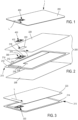
- the example of smart card 1 shown in the figure 1 comprises a card body 200 and a module 400.
- a smart card 1 can be manufactured using several methods.
- the lower layer 205 is, for example, a finishing layer (for example, printing) and protection of the card 1. It is located under the antenna support 210. It is made of PVC and its thickness is, for example, 0.20 mm, before lamination, and 0.18 mm, after lamination. The thickness of this lower layer 205 is uniform.
- the antenna support 210 comprises a PVC substrate 212, for example 0.43 mm thick, before lamination, and 0.40 mm thick, after lamination.
- a wire antenna 214 for example is deposited and fixed to the substrate 212 (for example embedded, by the technique called in English “wire embedding”). This antenna 214 is formed of several wound turns and ends with two ends 216, 218.
- the connection unit 300 comprises a flexible film 310 with a first and a second main face (see also figure 5 ).
- a conductive layer 312 is laminated on one of these main faces.
- the substrate 310 is for example made of a material of the FR4 or VEP (glass-epoxy) type, 0.075 mm thick (and more generally less than or equal to 0.1 mm).
- the conductive layer 312 is for example made of a copper alloy in a sheet 0.03 mm thick.
- the flexible film 310 is therefore for example of the copper-clad laminate type.
- connection unit 300 has, for example, a length of 18 mm and a width of 4.5 mm. An opening 314 of 8 mm by 4 mm, for example, is cut substantially in the middle of the connection unit 300.
- the connection unit 300 comprises two connection pads 316. Each connection pad 316 comprises a first 317 and a second 319 portion, electrically connected to each other (see also figure 5 ).
- the first portion 317 has an essentially rectangular shape.
- the second portion 319 has, for example, a U shape extending around the openings 314, with the bottom of the U connected (connected) essentially to the middle of the first portion 317 considered in its longitudinal direction.
- each connection pad has an “H” shape with each of the parallel branches of the “H” corresponding respectively to a first or a second portion of the metallized zone, these first and second portions being connected by the middle branch.
- connection units 300 are produced (for example continuously, from reel to reel), from a flexible film 310.
- This flexible film 310 is cut (for example by punching) to form the openings 314 intended to receive the encapsulation resin of a module 400, as explained later.
- Drive notches are also cut.
- the conductive layer is then etched (for example using photolithography techniques) to form the connection pads 316 (two connection pads 316 per connection unit 300), with their first 317 and second 319 portions.
- solder material 350 is then deposited on each of the first 317 and second 319 portions of the connection pads 316, for example to a thickness of for example between 0.02 and 0.5 mm.
- the solder material 350 is for example made of a tin-bismuth alloy.
- the solder material 350 is then removed from the first portions 317.
- the connection units 300 are cut to be individualized.
- the solder material 350 is deposited more selectively, for example in the form of a drop of solder, only on each of the second portions 319 of the connection pads 316.
- solder material 350 on the second portions 319 (but as indicated above possibly also on the first portions 317) of the conductive layer of the connection pads 316 is carried out for example by dispensing, by screen printing or even by the so-called “wave” technology (this technology makes it possible to deposit solder material 350 on thicknesses of the order of 100 or 200 ⁇ m, or even less, and on small surfaces, such as 3x4 mm 2 for example).
- Each drop of solder material 350 once deposited on a second portion 319 and before the heating operation to perform the soldering between the connection unit 300 and the module 400, forms a dome having a height of between 0.02 and 0.5 mm.
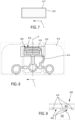
- connection pads 416 Each drop of solder material 350, during heating, must come into contact with the connection pads 416 (see figures 6 to 8 ).
- the wettability of the molten solder material 350 may possibly be sufficient to establish the connection, even in cases where a drop of solder material 350 would only surface on the surface of the cavity 410 on which the module 400 is housed (see figures 2 And 4 ).
- insufficient or faulty contact due to insufficient wettability can be avoided by adapting the height of each drop of solder material 350 so that this height is greater than the distance which separates the top of the drop of solder material 350 from the connection pad 416 located under the module 400.
- connection unit 300 (possibly glued) on or in the antenna support 210
- the ends 216, 218 of the antenna 214 are connected (for example by thermocompression) to the first portions 317 of the connection pads 316.
- This assembly consisting of the antenna 214 and the connection unit 300 on the support 210, can be covered with a layer of plastic material to form a structure that can be sold to be laminated with one or more other layers of plastic material in order to produce a smart card 1.
- the antenna support 210 can be composed of at least two sub-layers.
- the antenna is inserted for example between the sub-layer below and the sub-layer above.
- the sub-layer above then comprises a cut-out for receiving a connection unit 300.
- the upper finishing and protective layer 220 is also, for example, made of PVC. It is 0.20 mm thick before lamination and 0.18 mm thick after lamination. This upper finishing and protective layer 220 comprises a cutout 222 corresponding to a cavity 410.
- the upper layer 220 is laminated with the antenna support 210 (and possibly the other constituent layers of the card body 200) without the latter being previously cut ( figure 3 ). Then, the cavity 410 is milled to reveal the second portions 319 of the connection pads before connecting and fixing the module 400 in the cavity 410.
- each drop of solder material 350 is removed, to ensure that the plastic material in which the milling is carried out will not prevent either the surfaces to be welded from coming together, or the material forming the drops of molten solder material 350 from wetting the conductive tracks of the module 400 on which they are to be welded.
- the first portions 317 of the connection pads 316, on which the ends 216, 218 of the antenna 214 have been connected, are located outside the milled area and remain protected by the upper layer 220.
- the bottom layer 205 and the top layer 220, as well as the antenna support 210 are not necessarily monolayers. Each of them may optionally be made of one or more layers, all laminated together in the finished board 1.
- the total thickness of all layers 205-220, and therefore of card 1, is approximately 0.8 mm after lamination.
- a module 400 is produced for example in a known manner on a substrate comprising contacts 412 on one face (called “contact face” or “front face”), and conductive tracks 414 (as well as an electronic chip not shown), on the other (called “rear face” or “bonding face”) (see figures 6 And 8 ).
- the fixing of the electronic chip on the substrate is carried out by at least one known technique such as die-attachment and its electrical connection to the conductive tracks 414 is carried out by at least one known technique such as flip-chip technology, wire-bonding, etc.
- the chip and its possible wire connections to the conductive tracks 414 are advantageously protected by encapsulation in a resin (globe top or dam&fill, corresponding to UV or thermal encapsulation).
- the chip being placed on the rear face of the substrate or in a cutout made in it, the encapsulation is carried out from this rear face and can form an excess thickness relative to it.
- connection pads 416 are used to solder the second portions 319 of the connection pads 316.
- the ends 216, 218 of the antenna 214 are themselves electrically connected to the first portions 317, connected to the second portions 319, which themselves are soldered to the connection pads 416 electrically connected on the rear face of the module 400 to the chip by the conductive tracks 414.
- each connection pad 416 extends in a zone 417 (delimited by dotted lines on the figure 7 ) covering a surface area smaller than that of the second portions 319 (on the figures 6 to 8 the second portions 319 are shown in the form of a hatched rectangle, but they may have other shapes, in particular the “U” shape shown in the preceding figures).
- the area 417 may be defined as that which contains bars 418 and the conductive tracks which connect the bars 418 together.
- the bars 418 are elongated in a direction L essentially perpendicular to the largest side of the module 400, which is generally intended to be parallel to the length of the card 1.
- the longitudinal direction L is shown in the Figures 1 to 4 .
- Each bar 418 is relatively thin so as to possibly be able to detach from the substrate of the module 400 to absorb, without breaking, a significant stress. It has a width l for example between 50 ⁇ m and 300 ⁇ m. More particularly, it can have a width close to 100 ⁇ m. Having a thin width allows them to possibly detach from the substrate 450 of the module 400.
- the 418 bars have for example a length between 1 and 7 mm.
- the 418 bars shown on the figures 6 And 8 are essentially straight, but they could be wavy, sinusoidal, etc.
- the bars 418 are essentially symmetrical with respect to a plane P perpendicular to the substrate of the module 400 and to the longitudinal direction L, and passing through the middle of the module 400.
- the bars 418 meet at each of their longitudinal ends and are connected to the conductive tracks 414.
- the ends of the latter terminate in curved portions 420.
- the radii of curvature of the curved portions make it possible to distribute the stresses over a greater length and a larger surface area.
- the bars 418 are three in number and the curved portions 420 of the longitudinal ends of the bars are directed towards the inside of the module.
- the two bars 418 furthest from the center of the module 400 have for example a width of 100 ⁇ m and the one closest to the center has a width of 150 ⁇ m.
- Their length is preferably between 1.5 and 3 mm; for example it is 2.5 mm.
- the module 400 is placed in the cavity 410, with the solder material 350, arranged on each of the second portions 319 of the connection pads 316, opposite the connection pads 416.
- the areas of the module 400 located at the level of the drops of solder material 350 are then heated, for example using a thermode, to melt the solder material 350 and solder the connection pads 316 to the connection pads 416 (This heating operation is optionally carried out at the same time as that consisting of heating areas of heat-reactivatable adhesive, very close to the drops of solder material allowing each module to be bonded in its cavity).
- a solder material 350 having a melting temperature of between 120°C and 230°C, and more preferably between 130 and 150°C the operation of heating the solder material 350 can be carried out by applying, with a thermode for example, to an area of the module 400, a temperature of between 120°C and 250°C.
- connection pad 416 Due to the thickness of the module 400 and the height of the dome of a drop of solder material 350, when the solder material melts, it wets the corresponding connection pad 416.
- the spaces between the bars 418 form grooves 422, delimited on the one hand by the sides corresponding to the thickness of the bars 418, and on the other hand, by the substrate 450 of the module 400.
- These grooves 422 make it possible to channel the solder material 350 and to prevent it from spreading widely outside the zone 417 in which a connection pad 416 is located.
- the solder between the connection pads 316 and the connection studs 416 can cover a surface area of at least the order of 2 mm 2 and is such that a sufficiently high tear-off force of the module 400 is obtained, to meet the specifications of this type of product.
- the solder material 350 thus optionally makes it possible, not only to establish an electrical connection between the connection pads 416 and the connection pads 316, but also to fix the module 400 in the cavity 410 without the aid of any other adhesive.
- a smart card structure 1 has been described in which a connection unit is used to make the connection between the antenna 214 and the module 400.
- the invention also applies to a structure in which an antenna and connection pads are located on the same substrate (for example the antenna and the connection pads are etched on the same substrate which then forms an antenna support 210).
Landscapes
- Engineering & Computer Science (AREA)
- Microelectronics & Electronic Packaging (AREA)
- Computer Hardware Design (AREA)
- Physics & Mathematics (AREA)
- General Physics & Mathematics (AREA)
- Theoretical Computer Science (AREA)
- Credit Cards Or The Like (AREA)
Claims (13)
- Verfahren zur Herstellung einer Smartcard, umfassend :- Herstellung eines Moduls (400) einer Chipkarte (1) mit einem Substrat (450) mit einer ersten und einer zweiten Hauptseite, mit Kontakten (412) auf der ersten Seite des Substrats und Leiterbahnen (414) mit Anschlussflächen (416) auf der zweiten Seite des Substrats, wobei dieses Modul auch mit einem elektronischen Chip (120) versehen ist, der mit mindestens bestimmten Kontakten (102) und mit mindestens zwei Leiterbahnen (414) verbunden ist, die einem Antennenanschluss gewidmet sind,- die Herstellung einer Antenne (214) mit zwei Enden (216, 218),- das Laminieren der Antenne (214) zwischen Kunststoffschichten (205, 220) und- Einsetzen des Moduls (400) in einen Hohlraum (410), der in mindestens einigen der Kunststoffschichten (220) ausgebildet ist,- das Verbinden mithilfe eines Lötmaterials, das auf einen Verbindungsabschnitt (319) jedes der Enden (216, 218) der Antenne (214) mit einer Fläche (416) des Moduls (400) aufgebracht und erhitzt wird, sobald das Modul (400) in dem Hohlraum (410) angeordnet ist,dadurch gekennzeichnet, dass die Verbindungsanschlußflächen (416) jeweils auf einem Bereich (417) ausgebildet sind, der eine Fläche abdeckt, die kleiner ist als die eines Anschlussabschnitts (319), der in einer leitfähigen Schicht ausgebildet und mit Lötmaterial (350) bedeckt ist.
- Verfahren nach Anspruch 1, wobei das Lötmaterial (350) aus einem Material mit einer Schmelztemperatur zwischen 120°C und 230°C und besonders bevorzugt zwischen 130°C und 150°C besteht.
- Verfahren nach einem der vorhergehenden Ansprüche, bei dem mindestens eine der Verbindungsanschlußflächen (416) mit mindestens einem Stab (418) hergestellt wird, der sich in Längsrichtung in einer Richtung (L) über eine Länge zwischen 1 und 7 mm erstreckt.
- Verfahren nach einem der vorhergehenden Ansprüche, bei dem man mindestens eine der Verbindungsanschlußflächen (416) mit mindestens einem Stab (418) herstellt, dessen Breite zwischen 50 und 300 µm liegt.
- Verfahren nach einem der vorhergehenden Ansprüche, bei dem mindestens eines der Verbindungsanschlußflächen (416) mit mindestens einem Stab (418) hergestellt wird, der sich in Längsrichtung in einer Richtung (L) erstreckt, die im Wesentlichen senkrecht zur Länge des Moduls (400) verläuft.
- Verfahren nach einem der vorhergehenden Ansprüche, bei dem mindestens eine der Verbindungsflächen (416) hergestellt wird, die mindestens einen Stab (418) umfasst, dessen Enden zum Inneren des Moduls (400) hin umgebogen sind.
- Verfahren nach einem der vorhergehenden Ansprüche, bei dem mindestens eines der der Verbindungsanschlußflächen (416) mit mindestens zwei Stäben (418) hergestellt wird, die an ihren Längsenden elektrisch verbunden sind.
- Verfahren nach einem der vorhergehenden Ansprüche, bei dem man eine Verbindungseinheit (300) herstellt und die Enden der Antenne (214) einerseits mit ersten Abschnitten (317) der Verbindungseinheit (300) verbindet und andererseits einen Tropfen Lötmaterial (350) auf zweite Abschnitte (319) der Verbindungseinheit (300) aufträgt, um eine Lötverbindung mit jedem der Verbindungsanschlußflächen (416) herzustellen.
- Smartcard bestehend aus :- eine Antenne (214) mit zwei Enden (216, 218),- Kunststoffschichten (205, 220), zwischen denen die Antenne (214) angeordnet ist, und- ein Modul (400), das ein Substrat (450) mit einer ersten und einer zweiten Hauptseite umfasst, wobei auf der ersten Seite des Substrats Kontakte (412) und auf der zweiten Seite des Substrats Leiterbahnen (414) mit Anschlussflecken (416) vorhanden sind, wobei dieses Modul auch mit einem elektronischen Chip versehen ist, der mit mindestens einigen Kontakten (412) und mindestens zwei Leiterbahnen (414) verbunden ist, die einer Antennenverbindung gewidmet sind, wobei das Modul (400) in einem Hohlraum (410) angeordnet ist, der in mindestens einigen der Kunststoffschichten (220) ausgebildet ist,- einen Verbindungsabschnitt (319), der mit jedem der Enden (216, 218) der Antenne (214) verbunden ist und Lötmaterial aufweist, das an eine Verbindungsanschlußflächen (416) des Moduls (400) gelötet ist,dadurch gekennzeichnet, dass die Verbindungsanschlußflächen (416) jeweils einen Bereich (417) mit einer Fläche bedecken, die kleiner ist als die eines Verbindungsabschnitts (319), der in einer leitfähigen Schicht ausgebildet und mit dem Lötmaterial (350) bedeckt ist.
- Smartcard nach Anspruch 9, wobei das Lötmaterial (350) aus einem Material mit einer Schmelztemperatur zwischen 120°C und 230°C und besonders bevorzugt zwischen 130°C und 150°C besteht.
- Chipkartenmodul zur Herstellung einer Chipkarte nach einem der Ansprüche 9 und 10, wobei dieses Modul ein Substrat (450) mit einer ersten und einer zweiten Hauptseite umfasst, wobei auf der ersten Seite des Substrats Kontakte (412) und auf der zweiten Seite des Substrats Leiterbahnen (414) mit Verbindungsanschlußflächen (416) vorhanden sind, wobei dieses Modul dazu bestimmt ist, mit einem elektronischen Chip versehen zu werden, der mit mindestens einigen Kontakten (412) und mindestens zwei Leiterbahnen (414) verbunden ist, die einer Antennenverbindung gewidmet sind, wobei dieses Modul auch dazu bestimmt ist, mit einem Verbindungsabschnitt (319) verbunden zu werden, der in einer leitenden Schicht ausgebildet ist und mit jedem der Enden (216, 218) einer Antenne (214) verbunden ist und Lötmaterial enthält,
wobei die Verbindungsflecken (416) jeweils einen Bereich (417) mit einer Fläche bedecken, die kleiner ist als die eines Verbindungsabschnitts (319), der mit dem Lötmaterial (350) bedeckt ist, und mindestens einer der Verbindungsanschlußflächen (416) mindestens einen Stab (418) aufweist, der sich in Längsrichtung in einer Richtung (L) über eine Länge von 1 bis 7 mm erstreckt und eine Breite von 50 bis 300 µm hat. - Smartcard-Modul nach Anspruch 11, wobei das Lötmaterial (350) aus einem Material mit einer Schmelztemperatur zwischen 120°C und 230°C und besonders bevorzugt zwischen 130°C und 150°C besteht.
- Chipkartenmodul nach einem der Ansprüche 11 oder 12, bei dem ein Fläche (416) mindestens zwei Stäbe (418) umfasst, deren Längsenden gebogen und elektrisch verbunden sind.
Applications Claiming Priority (2)
| Application Number | Priority Date | Filing Date | Title |
|---|---|---|---|
| FR1654102A FR3051063B1 (fr) | 2016-05-06 | 2016-05-06 | Procede de fabrication de cartes a puce et carte a puce obtenue par ce procede |
| PCT/FR2017/051063 WO2017191414A1 (fr) | 2016-05-06 | 2017-05-03 | Procédé de fabrication de cartes à puce et carte à puce obtenue par ce procédé |
Publications (2)
| Publication Number | Publication Date |
|---|---|
| EP3452958A1 EP3452958A1 (de) | 2019-03-13 |
| EP3452958B1 true EP3452958B1 (de) | 2025-01-15 |
Family
ID=56322183
Family Applications (1)
| Application Number | Title | Priority Date | Filing Date |
|---|---|---|---|
| EP17725331.7A Active EP3452958B1 (de) | 2016-05-06 | 2017-05-03 | Verfahren zur herstellung von chipkarten und durch besagtes verfahren erhaltene chipkarte |
Country Status (4)
| Country | Link |
|---|---|
| US (1) | US10804226B2 (de) |
| EP (1) | EP3452958B1 (de) |
| FR (1) | FR3051063B1 (de) |
| WO (1) | WO2017191414A1 (de) |
Families Citing this family (2)
| Publication number | Priority date | Publication date | Assignee | Title |
|---|---|---|---|---|
| FR3063555B1 (fr) * | 2017-03-03 | 2021-07-09 | Linxens Holding | Carte a puce et procede de fabrication d’une carte a puce |
| FR3082696B1 (fr) | 2018-06-15 | 2020-09-11 | Linxens Holding | Procede de fabrication d'un support en rouleau pour composant electroniques, d'un module de carte a puce et d'une carte a puce, ainsi que support pour composants electroniques |
Citations (2)
| Publication number | Priority date | Publication date | Assignee | Title |
|---|---|---|---|---|
| FR2880160B1 (fr) * | 2004-12-28 | 2007-03-30 | K Sa As | Module electronique double face pour carte a puce hybride |
| EP2677476A1 (de) * | 2012-06-21 | 2013-12-25 | Gemalto SA | Verbindungsverfahren mit Hilfe einer Spule aus mit leitendem Material ummanteltem, geschweißtem Draht, und so erhaltene Vorrichtung |
Family Cites Families (11)
| Publication number | Priority date | Publication date | Assignee | Title |
|---|---|---|---|---|
| JP4299414B2 (ja) * | 1999-10-12 | 2009-07-22 | 富士通マイクロエレクトロニクス株式会社 | コンビネーションカード、icカード用モジュール及びコンビネーションカードの製造方法 |
| FR2801707B1 (fr) * | 1999-11-29 | 2002-02-15 | A S K | Procede de fabrication d'une carte a puce hybride contact- sans contact avec un support d'antenne en materiau fibreux |
| JP2001358517A (ja) * | 2000-06-15 | 2001-12-26 | Murata Mfg Co Ltd | アンテナ装置およびそれを用いた無線機 |
| US20030141103A1 (en) * | 2002-01-31 | 2003-07-31 | Ng Wee Lee | PCB solder pad geometry including patterns improving solder coverage |
| DE60326598D1 (de) * | 2002-08-26 | 2009-04-23 | Dainippon Printing Co Ltd | Sim, ic-modul und ic-karte |
| FR2863747B1 (fr) | 2003-12-11 | 2006-03-24 | Oberthur Card Syst Sa | Fiabilisation des cartes dual interface par grille continue |
| US7980477B2 (en) * | 2007-05-17 | 2011-07-19 | Féinics Amatech Teoranta | Dual interface inlays |
| US20120248201A1 (en) * | 2011-01-31 | 2012-10-04 | American Bank Note Company | Dual-interface smart card |
| FR3013504B1 (fr) | 2013-11-18 | 2022-06-10 | Interplex Microtech | Procede de fabrication d'un support d'une puce electronique, support de puce et ensemble de tels supports |
| FR3021145B1 (fr) * | 2014-05-14 | 2018-08-31 | Linxens Holding | Procede de fabrication d'un circuit pour module de carte a puce et circuit pour module de carte a puce |
| FR3026529B1 (fr) | 2014-09-30 | 2017-12-29 | Linxens Holding | Procede de fabrication de carte a puce et carte a puce obtenue par ce procede. |
-
2016
- 2016-05-06 FR FR1654102A patent/FR3051063B1/fr not_active Expired - Fee Related
-
2017
- 2017-05-03 US US16/098,203 patent/US10804226B2/en active Active
- 2017-05-03 WO PCT/FR2017/051063 patent/WO2017191414A1/fr not_active Ceased
- 2017-05-03 EP EP17725331.7A patent/EP3452958B1/de active Active
Patent Citations (2)
| Publication number | Priority date | Publication date | Assignee | Title |
|---|---|---|---|---|
| FR2880160B1 (fr) * | 2004-12-28 | 2007-03-30 | K Sa As | Module electronique double face pour carte a puce hybride |
| EP2677476A1 (de) * | 2012-06-21 | 2013-12-25 | Gemalto SA | Verbindungsverfahren mit Hilfe einer Spule aus mit leitendem Material ummanteltem, geschweißtem Draht, und so erhaltene Vorrichtung |
Also Published As
| Publication number | Publication date |
|---|---|
| US10804226B2 (en) | 2020-10-13 |
| FR3051063A1 (fr) | 2017-11-10 |
| US20190157223A1 (en) | 2019-05-23 |
| FR3051063B1 (fr) | 2021-02-12 |
| WO2017191414A1 (fr) | 2017-11-09 |
| EP3452958A1 (de) | 2019-03-13 |
Similar Documents
| Publication | Publication Date | Title |
|---|---|---|
| EP3437028B1 (de) | Verfahren zur herstellung von chipkarten und von chipkartenantennenträgern | |
| EP3201843B1 (de) | Chipkartenherstellungsverfahren und durch besagtes verfahren erhaltene chipkarte | |
| EP3143557B1 (de) | Verfahren zur herstellung einer schaltung für ein chipkartenmodul und schaltung für ein chipkartenmodul | |
| EP2877965B1 (de) | Elektronisches modul für eine chipkarte und gedruckte schaltung zur erzeugung eines solchen moduls | |
| CA2805201A1 (fr) | Dispositif d'identification radio frequence en polycarbonate et son procede de fabrication | |
| EP1076882B1 (de) | Chipkarte mit leiterrahmen und verfahren zur herstellung einer solchen karte | |
| WO2014191428A1 (fr) | Procédé de fabrication d'un circuit imprimé, circuit imprimé obtenu par ce procédé et module électronique comportant un tel circuit imprimé | |
| EP3408799B1 (de) | Verfahren zur herstellung eines chipkartenmoduls und chipkarte | |
| EP2937823B1 (de) | Herstellungsverfahren einer struktur für chipkarten, und mit diesem verfahren erhaltene struktur für chipkarte | |
| EP3452958B1 (de) | Verfahren zur herstellung von chipkarten und durch besagtes verfahren erhaltene chipkarte | |
| EP3020256B1 (de) | Elektronisches modul mit klebende dielektrische beschichtung, und sein herstellungsverfahren | |
| EP1846874B1 (de) | Verfahren zur anbringung einer elektronischen baugruppe an einem substrat und einrichtung zur anbringung der baugruppe | |
| EP2866173B1 (de) | Verfahren zur Erzeugung eines elektrischen Schaltkreises, und mit diesem Verfahren erzeugter Schaltkreis | |
| WO2004100063A1 (fr) | Procede de fabrication d'un inlet prelamine | |
| FR2795199A1 (fr) | Dispositif et procede de fabrication de dispositifs comprenant au moins une puce montee sur un support | |
| EP0969410B1 (de) | Chipkarte mit Antenne | |
| EP3651068A1 (de) | Verfahren zur herstellung eines elektronischen einsatzes für tragbare multikomponenten-halterung, und so erhaltener einsatz | |
| EP2825001A1 (de) | Elektronisches Modul mit klebende dielektrische Beschichtung, und sein Herstellungsverfahren | |
| EP4293569B1 (de) | Inlay für ein elektronisches dokument, verfahren zur herstellung eines elektronischen dokuments mit einem solchen inlay und dieses elektronische dokument | |
| WO2002037553A1 (fr) | Connexion de circuit integre par depôt conducteur a travers un film perfore |
Legal Events
| Date | Code | Title | Description |
|---|---|---|---|
| STAA | Information on the status of an ep patent application or granted ep patent |
Free format text: STATUS: UNKNOWN |
|
| STAA | Information on the status of an ep patent application or granted ep patent |
Free format text: STATUS: THE INTERNATIONAL PUBLICATION HAS BEEN MADE |
|
| PUAI | Public reference made under article 153(3) epc to a published international application that has entered the european phase |
Free format text: ORIGINAL CODE: 0009012 |
|
| STAA | Information on the status of an ep patent application or granted ep patent |
Free format text: STATUS: REQUEST FOR EXAMINATION WAS MADE |
|
| 17P | Request for examination filed |
Effective date: 20181017 |
|
| AK | Designated contracting states |
Kind code of ref document: A1 Designated state(s): AL AT BE BG CH CY CZ DE DK EE ES FI FR GB GR HR HU IE IS IT LI LT LU LV MC MK MT NL NO PL PT RO RS SE SI SK SM TR |
|
| AX | Request for extension of the european patent |
Extension state: BA ME |
|
| DAV | Request for validation of the european patent (deleted) | ||
| DAX | Request for extension of the european patent (deleted) | ||
| STAA | Information on the status of an ep patent application or granted ep patent |
Free format text: STATUS: EXAMINATION IS IN PROGRESS |
|
| 17Q | First examination report despatched |
Effective date: 20200630 |
|
| P01 | Opt-out of the competence of the unified patent court (upc) registered |
Effective date: 20230425 |
|
| GRAP | Despatch of communication of intention to grant a patent |
Free format text: ORIGINAL CODE: EPIDOSNIGR1 |
|
| STAA | Information on the status of an ep patent application or granted ep patent |
Free format text: STATUS: GRANT OF PATENT IS INTENDED |
|
| INTG | Intention to grant announced |
Effective date: 20241031 |
|
| GRAS | Grant fee paid |
Free format text: ORIGINAL CODE: EPIDOSNIGR3 |
|
| GRAA | (expected) grant |
Free format text: ORIGINAL CODE: 0009210 |
|
| STAA | Information on the status of an ep patent application or granted ep patent |
Free format text: STATUS: THE PATENT HAS BEEN GRANTED |
|
| AK | Designated contracting states |
Kind code of ref document: B1 Designated state(s): AL AT BE BG CH CY CZ DE DK EE ES FI FR GB GR HR HU IE IS IT LI LT LU LV MC MK MT NL NO PL PT RO RS SE SI SK SM TR |
|
| REG | Reference to a national code |
Ref country code: CH Ref legal event code: EP Ref country code: GB Ref legal event code: FG4D Free format text: NOT ENGLISH |
|
| REG | Reference to a national code |
Ref country code: DE Ref legal event code: R096 Ref document number: 602017087334 Country of ref document: DE |
|
| REG | Reference to a national code |
Ref country code: IE Ref legal event code: FG4D Free format text: LANGUAGE OF EP DOCUMENT: FRENCH |
|
| REG | Reference to a national code |
Ref country code: NL Ref legal event code: FP |
|
| PGFP | Annual fee paid to national office [announced via postgrant information from national office to epo] |
Ref country code: NL Payment date: 20250522 Year of fee payment: 9 |
|
| PG25 | Lapsed in a contracting state [announced via postgrant information from national office to epo] |
Ref country code: RS Free format text: LAPSE BECAUSE OF FAILURE TO SUBMIT A TRANSLATION OF THE DESCRIPTION OR TO PAY THE FEE WITHIN THE PRESCRIBED TIME-LIMIT Effective date: 20250415 |
|
| PG25 | Lapsed in a contracting state [announced via postgrant information from national office to epo] |
Ref country code: FI Free format text: LAPSE BECAUSE OF FAILURE TO SUBMIT A TRANSLATION OF THE DESCRIPTION OR TO PAY THE FEE WITHIN THE PRESCRIBED TIME-LIMIT Effective date: 20250115 |
|
| PG25 | Lapsed in a contracting state [announced via postgrant information from national office to epo] |
Ref country code: PL Free format text: LAPSE BECAUSE OF FAILURE TO SUBMIT A TRANSLATION OF THE DESCRIPTION OR TO PAY THE FEE WITHIN THE PRESCRIBED TIME-LIMIT Effective date: 20250115 |
|
| PGFP | Annual fee paid to national office [announced via postgrant information from national office to epo] |
Ref country code: DE Payment date: 20250519 Year of fee payment: 9 |
|
| PG25 | Lapsed in a contracting state [announced via postgrant information from national office to epo] |
Ref country code: ES Free format text: LAPSE BECAUSE OF FAILURE TO SUBMIT A TRANSLATION OF THE DESCRIPTION OR TO PAY THE FEE WITHIN THE PRESCRIBED TIME-LIMIT Effective date: 20250115 |
|
| PGFP | Annual fee paid to national office [announced via postgrant information from national office to epo] |
Ref country code: GB Payment date: 20250522 Year of fee payment: 9 |
|
| REG | Reference to a national code |
Ref country code: LT Ref legal event code: MG9D |
|
| PG25 | Lapsed in a contracting state [announced via postgrant information from national office to epo] |
Ref country code: NO Free format text: LAPSE BECAUSE OF FAILURE TO SUBMIT A TRANSLATION OF THE DESCRIPTION OR TO PAY THE FEE WITHIN THE PRESCRIBED TIME-LIMIT Effective date: 20250415 Ref country code: IS Free format text: LAPSE BECAUSE OF FAILURE TO SUBMIT A TRANSLATION OF THE DESCRIPTION OR TO PAY THE FEE WITHIN THE PRESCRIBED TIME-LIMIT Effective date: 20250515 |
|
| REG | Reference to a national code |
Ref country code: AT Ref legal event code: MK05 Ref document number: 1760304 Country of ref document: AT Kind code of ref document: T Effective date: 20250115 |
|
| PG25 | Lapsed in a contracting state [announced via postgrant information from national office to epo] |
Ref country code: HR Free format text: LAPSE BECAUSE OF FAILURE TO SUBMIT A TRANSLATION OF THE DESCRIPTION OR TO PAY THE FEE WITHIN THE PRESCRIBED TIME-LIMIT Effective date: 20250115 |
|
| PG25 | Lapsed in a contracting state [announced via postgrant information from national office to epo] |
Ref country code: PT Free format text: LAPSE BECAUSE OF FAILURE TO SUBMIT A TRANSLATION OF THE DESCRIPTION OR TO PAY THE FEE WITHIN THE PRESCRIBED TIME-LIMIT Effective date: 20250515 Ref country code: LV Free format text: LAPSE BECAUSE OF FAILURE TO SUBMIT A TRANSLATION OF THE DESCRIPTION OR TO PAY THE FEE WITHIN THE PRESCRIBED TIME-LIMIT Effective date: 20250115 |
|
| PGFP | Annual fee paid to national office [announced via postgrant information from national office to epo] |
Ref country code: FR Payment date: 20250523 Year of fee payment: 9 |
|
| PG25 | Lapsed in a contracting state [announced via postgrant information from national office to epo] |
Ref country code: BG Free format text: LAPSE BECAUSE OF FAILURE TO SUBMIT A TRANSLATION OF THE DESCRIPTION OR TO PAY THE FEE WITHIN THE PRESCRIBED TIME-LIMIT Effective date: 20250115 Ref country code: GR Free format text: LAPSE BECAUSE OF FAILURE TO SUBMIT A TRANSLATION OF THE DESCRIPTION OR TO PAY THE FEE WITHIN THE PRESCRIBED TIME-LIMIT Effective date: 20250416 |
|
| PG25 | Lapsed in a contracting state [announced via postgrant information from national office to epo] |
Ref country code: AT Free format text: LAPSE BECAUSE OF FAILURE TO SUBMIT A TRANSLATION OF THE DESCRIPTION OR TO PAY THE FEE WITHIN THE PRESCRIBED TIME-LIMIT Effective date: 20250115 |
|
| PG25 | Lapsed in a contracting state [announced via postgrant information from national office to epo] |
Ref country code: SE Free format text: LAPSE BECAUSE OF FAILURE TO SUBMIT A TRANSLATION OF THE DESCRIPTION OR TO PAY THE FEE WITHIN THE PRESCRIBED TIME-LIMIT Effective date: 20250115 |
|
| PG25 | Lapsed in a contracting state [announced via postgrant information from national office to epo] |
Ref country code: SM Free format text: LAPSE BECAUSE OF FAILURE TO SUBMIT A TRANSLATION OF THE DESCRIPTION OR TO PAY THE FEE WITHIN THE PRESCRIBED TIME-LIMIT Effective date: 20250115 |
|
| PG25 | Lapsed in a contracting state [announced via postgrant information from national office to epo] |
Ref country code: DK Free format text: LAPSE BECAUSE OF FAILURE TO SUBMIT A TRANSLATION OF THE DESCRIPTION OR TO PAY THE FEE WITHIN THE PRESCRIBED TIME-LIMIT Effective date: 20250115 |
|
| PG25 | Lapsed in a contracting state [announced via postgrant information from national office to epo] |
Ref country code: IT Free format text: LAPSE BECAUSE OF FAILURE TO SUBMIT A TRANSLATION OF THE DESCRIPTION OR TO PAY THE FEE WITHIN THE PRESCRIBED TIME-LIMIT Effective date: 20250115 |
|
| REG | Reference to a national code |
Ref country code: DE Ref legal event code: R097 Ref document number: 602017087334 Country of ref document: DE |
|
| PG25 | Lapsed in a contracting state [announced via postgrant information from national office to epo] |
Ref country code: CZ Free format text: LAPSE BECAUSE OF FAILURE TO SUBMIT A TRANSLATION OF THE DESCRIPTION OR TO PAY THE FEE WITHIN THE PRESCRIBED TIME-LIMIT Effective date: 20250115 Ref country code: EE Free format text: LAPSE BECAUSE OF FAILURE TO SUBMIT A TRANSLATION OF THE DESCRIPTION OR TO PAY THE FEE WITHIN THE PRESCRIBED TIME-LIMIT Effective date: 20250115 |
|
| PG25 | Lapsed in a contracting state [announced via postgrant information from national office to epo] |
Ref country code: RO Free format text: LAPSE BECAUSE OF FAILURE TO SUBMIT A TRANSLATION OF THE DESCRIPTION OR TO PAY THE FEE WITHIN THE PRESCRIBED TIME-LIMIT Effective date: 20250115 |
|
| PG25 | Lapsed in a contracting state [announced via postgrant information from national office to epo] |
Ref country code: SK Free format text: LAPSE BECAUSE OF FAILURE TO SUBMIT A TRANSLATION OF THE DESCRIPTION OR TO PAY THE FEE WITHIN THE PRESCRIBED TIME-LIMIT Effective date: 20250115 |
|
| PLBE | No opposition filed within time limit |
Free format text: ORIGINAL CODE: 0009261 |
|
| STAA | Information on the status of an ep patent application or granted ep patent |
Free format text: STATUS: NO OPPOSITION FILED WITHIN TIME LIMIT |
|
| REG | Reference to a national code |
Ref country code: CH Ref legal event code: L10 Free format text: ST27 STATUS EVENT CODE: U-0-0-L10-L00 (AS PROVIDED BY THE NATIONAL OFFICE) Effective date: 20251126 |
|
| REG | Reference to a national code |
Ref country code: CH Ref legal event code: H13 Free format text: ST27 STATUS EVENT CODE: U-0-0-H10-H13 (AS PROVIDED BY THE NATIONAL OFFICE) Effective date: 20251223 |
|
| 26N | No opposition filed |
Effective date: 20251016 |
|
| PG25 | Lapsed in a contracting state [announced via postgrant information from national office to epo] |
Ref country code: LU Free format text: LAPSE BECAUSE OF NON-PAYMENT OF DUE FEES Effective date: 20250503 |
|
| PG25 | Lapsed in a contracting state [announced via postgrant information from national office to epo] |
Ref country code: CH Free format text: LAPSE BECAUSE OF NON-PAYMENT OF DUE FEES Effective date: 20250531 |
|
| REG | Reference to a national code |
Ref country code: BE Ref legal event code: MM Effective date: 20250531 |
|
| PG25 | Lapsed in a contracting state [announced via postgrant information from national office to epo] |
Ref country code: MC Free format text: LAPSE BECAUSE OF FAILURE TO SUBMIT A TRANSLATION OF THE DESCRIPTION OR TO PAY THE FEE WITHIN THE PRESCRIBED TIME-LIMIT Effective date: 20250115 |
|
| PG25 | Lapsed in a contracting state [announced via postgrant information from national office to epo] |
Ref country code: IE Free format text: LAPSE BECAUSE OF NON-PAYMENT OF DUE FEES Effective date: 20250503 |
|
| PG25 | Lapsed in a contracting state [announced via postgrant information from national office to epo] |
Ref country code: BE Free format text: LAPSE BECAUSE OF NON-PAYMENT OF DUE FEES Effective date: 20250531 |