EP3651068A1 - Verfahren zur herstellung eines elektronischen einsatzes für tragbare multikomponenten-halterung, und so erhaltener einsatz - Google Patents
Verfahren zur herstellung eines elektronischen einsatzes für tragbare multikomponenten-halterung, und so erhaltener einsatz Download PDFInfo
- Publication number
- EP3651068A1 EP3651068A1 EP18306481.5A EP18306481A EP3651068A1 EP 3651068 A1 EP3651068 A1 EP 3651068A1 EP 18306481 A EP18306481 A EP 18306481A EP 3651068 A1 EP3651068 A1 EP 3651068A1
- Authority
- EP
- European Patent Office
- Prior art keywords
- printed circuit
- bridges
- circuit
- electrical
- frame structure
- Prior art date
- Legal status (The legal status is an assumption and is not a legal conclusion. Google has not performed a legal analysis and makes no representation as to the accuracy of the status listed.)
- Withdrawn
Links
Images




Classifications
-
- G—PHYSICS
- G06—COMPUTING OR CALCULATING; COUNTING
- G06K—GRAPHICAL DATA READING; PRESENTATION OF DATA; RECORD CARRIERS; HANDLING RECORD CARRIERS
- G06K19/00—Record carriers for use with machines and with at least a part designed to carry digital markings
- G06K19/06—Record carriers for use with machines and with at least a part designed to carry digital markings characterised by the kind of the digital marking, e.g. shape, nature, code
- G06K19/067—Record carriers with conductive marks, printed circuits or semiconductor circuit elements, e.g. credit or identity cards also with resonating or responding marks without active components
- G06K19/07—Record carriers with conductive marks, printed circuits or semiconductor circuit elements, e.g. credit or identity cards also with resonating or responding marks without active components with integrated circuit chips
- G06K19/077—Constructional details, e.g. mounting of circuits in the carrier
- G06K19/07749—Constructional details, e.g. mounting of circuits in the carrier the record carrier being capable of non-contact communication, e.g. constructional details of the antenna of a non-contact smart card
- G06K19/0775—Constructional details, e.g. mounting of circuits in the carrier the record carrier being capable of non-contact communication, e.g. constructional details of the antenna of a non-contact smart card arrangements for connecting the integrated circuit to the antenna
- G06K19/07754—Constructional details, e.g. mounting of circuits in the carrier the record carrier being capable of non-contact communication, e.g. constructional details of the antenna of a non-contact smart card arrangements for connecting the integrated circuit to the antenna the connection being galvanic
-
- G—PHYSICS
- G06—COMPUTING OR CALCULATING; COUNTING
- G06K—GRAPHICAL DATA READING; PRESENTATION OF DATA; RECORD CARRIERS; HANDLING RECORD CARRIERS
- G06K19/00—Record carriers for use with machines and with at least a part designed to carry digital markings
- G06K19/06—Record carriers for use with machines and with at least a part designed to carry digital markings characterised by the kind of the digital marking, e.g. shape, nature, code
- G06K19/067—Record carriers with conductive marks, printed circuits or semiconductor circuit elements, e.g. credit or identity cards also with resonating or responding marks without active components
- G06K19/07—Record carriers with conductive marks, printed circuits or semiconductor circuit elements, e.g. credit or identity cards also with resonating or responding marks without active components with integrated circuit chips
- G06K19/077—Constructional details, e.g. mounting of circuits in the carrier
- G06K19/07745—Mounting details of integrated circuit chips
-
- G—PHYSICS
- G06—COMPUTING OR CALCULATING; COUNTING
- G06K—GRAPHICAL DATA READING; PRESENTATION OF DATA; RECORD CARRIERS; HANDLING RECORD CARRIERS
- G06K19/00—Record carriers for use with machines and with at least a part designed to carry digital markings
- G06K19/06—Record carriers for use with machines and with at least a part designed to carry digital markings characterised by the kind of the digital marking, e.g. shape, nature, code
- G06K19/067—Record carriers with conductive marks, printed circuits or semiconductor circuit elements, e.g. credit or identity cards also with resonating or responding marks without active components
- G06K19/07—Record carriers with conductive marks, printed circuits or semiconductor circuit elements, e.g. credit or identity cards also with resonating or responding marks without active components with integrated circuit chips
- G06K19/077—Constructional details, e.g. mounting of circuits in the carrier
- G06K19/07749—Constructional details, e.g. mounting of circuits in the carrier the record carrier being capable of non-contact communication, e.g. constructional details of the antenna of a non-contact smart card
- G06K19/0775—Constructional details, e.g. mounting of circuits in the carrier the record carrier being capable of non-contact communication, e.g. constructional details of the antenna of a non-contact smart card arrangements for connecting the integrated circuit to the antenna
- G06K19/07756—Constructional details, e.g. mounting of circuits in the carrier the record carrier being capable of non-contact communication, e.g. constructional details of the antenna of a non-contact smart card arrangements for connecting the integrated circuit to the antenna the connection being non-galvanic, e.g. capacitive
Definitions
- the invention relates to a method of manufacturing electronic inserts for complex multi-component portable media.
- Such inserts are used in the manufacture of complex portable media such as multi-component smart cards using a hot or cold lamination or lamination process incorporating electronic inlay.
- the targeted method of producing an insert comprises a step of fixing a printed circuit in a housing or location of a frame structure, bridges positioning said circuit relative to the frame structure.
- the printed circuit intended by the invention can be connected or support various components such as a radiofrequency communication antenna and / or a keyboard and / or a radiofrequency microcircuit, a display (or screen), a biometric sensor, a switch, single-use number generator (OTP), a contact or contactless smart card module.
- the printed circuit can preferably comprise a thin insulating substrate of less than 50 ⁇ m and flexible.
- the insert can include energy storage elements such as a battery, a super capacity.
- the targeted printed circuit can cover an area greater than at least two modules with smart card contacts (or even 4 or more). For example, it can extend over a major surface of the smart card (having a length of approximately 2-7 cm and a width of approximately 2-4 cm)
- the insert may include an antenna connected to an electronic microcircuit. It may be intended to form, in particular by lamination with other sheets or by overmolding with resin, a portable multi-component radiofrequency support such as than a cover, an electronic passport sheet, an identity card, a bank chip card, any product with a radio frequency communication function. The thickness of the insert therefore matters.
- the insert somehow forms an intermediate product or by-product of a final multi-component product.
- the patent EP2036008 (B1 ) describes a method for producing an insert intended for the manufacture of multicomponent supports such as electronic chip cards.
- the inserts obtained according to this process can be manufactured from sheets with for example several rows of several tens of cards per sheet, as shown in the figure 1 and 2 .
- the method uses a plate with a plurality of openings (or housings) housing a plurality of multi-component electronic modules. These electronic modules are assembled to the plate with electrically insulating bridges and leaving a window over most of the surround of the electronic module. Subsequently, a filling material fills most of the space remaining in the openings and on the electronic module, to form an intermediate product after cutting.
- the patent US8305764 (B2 ) describes a process similar to the above patent. It illustrates the fact that the known inserts for radio frequency cards are generally formed with the main communication antenna, for example for banking transactions (EMV type), on the flexible printed circuit before being incorporated in a housing of frame structure ( or plate mentioned above).
- EMV type banking transactions
- the patent EP2232963 (B1 ) describes a method for producing a device comprising at least two separate components interconnected on a substrate by at least one interconnection wire.
- the method provides for making the interconnection wire by depositing individual wire on the substrate according to a predefined interconnection pattern;
- the wire comprises at least one terminal connection portion exposed on the substrate and at least one contact of a component is transferred opposite the terminal portion and then connected to this terminal portion.
- the patent US6233818 (B1 ) describes a method for producing a support comprising a radio frequency chip connected to an antenna. It describes making the antenna by embedding conductive wire on the support and overflowing the antenna wire above a cavity for receiving the chip and the connection pads of the chip. The wire is encrusted before and after the cavity. The studs access the wire through the cavity. The electrical connection of the wire to the studs is then carried out by thermocompression or ultrasound.
- a multi-component electronic support such as a display card and / or a biometric card is quite complex and expensive. It requires several manual operations which make manufacturing in volume, difficult and expensive.
- one of the options of the patent process EP2036008 may consist of using portions of adhesive tape ( fig. 2 ) which prevent any movement of the flexible printed circuit in its housing of the frame structure, during the flow of resin on and around the printed circuit or manipulation of the frame structure.
- the minimum number of servings of tape is most of the time three ( fig. 2 ).
- the fixing of these portions of adhesive tape is essentially manual and the flow rate is low.
- the radio frequency inserts are generally formed with the main communication antenna in the printed circuit intended to be integrated into a frame structure
- the antenna generally has the largest possible periphery for performance reasons; This generates a flexible printed circuit of very large area with a significant resulting cost because generally produced by copper etching.
- the antenna is practically close and set back from the external periphery of a framework structure (or card edge obtained with the insert). Due to the large surface area of the printed circuit, there are also difficulties in handling with machines in the chip card industry which are not suitable for integration into an insert.
- connection of the antenna to a radio frequency microcircuit is quite complex to carry out, the antenna being at the heart of the card in depth for reasons of the final visual of the product.
- the invention aims to solve the above problems.
- the invention provides a manufacturing method for automating and simplifying the steps for manufacturing a multi-component insert for a complex chip support (with or without antenna).
- the invention also aims to solve the aforementioned drawbacks of the cost and performance of the radiofrequency function in a multi-component insert.
- the invention also aims to facilitate the connection of an antenna to the flexible printed circuit or microcircuit in the context of the production of a low-cost and low-cost radiofrequency electronic insert having good communication performance, in particular of range.
- the inventors have found that it is preferable not to put a main communication antenna (of large area), on the flexible printed circuit for reasons of cost and radio frequency performance, but on the frame containing the printed circuit. This also makes it possible to have a flexible printed circuit of smaller size more easily integrated into an insert.
- the antenna is produced in the form of a conductive wire, in particular by a well-known technique of inlaying a wire, rather than via electrochemical etching, which further improves the electrical conductivity and the performances.
- the invention provides for using the technique of ultrasonic inlaying of conductive wire to maintain in position flexible multi-component printed circuits, relative to a framework structure, in particular in a housing ( window or location) of a frame structure or plate.
- the subject of the invention is a method for producing an electronic insert for a multi-component portable support, said method comprising a step of fixing a multi-component printed circuit in a housing or a location for a frame structure, bridges positioning said printed circuit relative to the frame structure;
- the method is characterized in that said bridges comprise electrical conductors.
- the method may further comprise the step of assembling said base sheet with said cover sheet by superimposing their respective recessed areas.
- the invention also relates to an insert corresponding to the process.
- the invention also relates to a multi-component portable device or support, such as a contactless smart card, a passport comprising the above insert or obtained according to the above method.
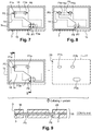
- FIGS. 1 and 2 illustrate the prior art; They describe to the figure 1 the supply of a plastic sheet 1 (or plate) comprising a plurality of housings L (windows or recesses) for the reception of a printed circuit 2 in each housing.
- Each printed circuit carries on a insulating substrate an etched main antenna 3 at the peripheral edge of the substrate.
- a space 4 surrounds each printed circuit in its housing.
- Adhesive tapes R1, R2, R3 are used to position and mechanically fix each printed circuit 2 in its housing L. The tapes form insulating bridges between the edges of the housings and each printed circuit.
- the method of the invention comprises, like the prior art above, a step of fixing a printed circuit in a housing or a location of a frame structure (or plate ), bridges positioning said circuit to the frame structure.
- a flexible printed circuit 2 is firstly fixed in a window L of a sheet of plastic material 1 (hereinafter interchangeably referred to as base sheet or "framework structure".
- the sheet 1 may have at least one housing L or preferably a plurality of housings L to form a set of electronic multi-component inserts after individualization by cutting.
- the printed circuits 2 within the meaning of the invention may comprise a flexible film (or substrate) carrying several electronic and / or electrical components which can be fixed or connected with known methods such as SMD, COB or Flip chip.
- the support film of the printed circuit supports at least two electronic components such as two integrated circuits or microcontrollers for example, a contactless smart card chip and a microcontroller for a biometric sensor and / or a single-use number generator. and / or a DCVV code generator (dynamically variable bank card cryptogram), and / or a display controller with at least two electronic microcontrollers.
- two integrated circuits or microcontrollers for example, a contactless smart card chip and a microcontroller for a biometric sensor and / or a single-use number generator. and / or a DCVV code generator (dynamically variable bank card cryptogram), and / or a display controller with at least two electronic microcontrollers.
- Printed circuits can be supplied with components soldered on them or just as an etched (or metallized) substrate with interconnecting conductive tracks and pads.
- Certain electronic components can be connected later when the printed circuit is in its housing or after stratification of layers by cavity machining and inserting, for example for an ISO 7816-2 smart card module or a display or a biometric sensor.
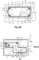
- the method can comprise, according to a first mode, either the supply or production (step 140 bis) of this framework structure ( figs. 3A, 3B, 3C , 12 ) with at least one (or more) housing (s) or location (s) of printed circuit (s)), i.e. the construction ( figs. 6-10 ; steps 100-140 figs. 13 ) of such a framework structure according to a second preferred mode, described below.
- the first mode provides in the illustrated examples ( figs. 3A-3C ), the supply (step 140bis, fig. 12 ) of a frame structure already having recessed areas, openings, surface windows each corresponding to receiving housings (or location) or space requirement of a printed circuit 2.
- the housings are made so as to have a clearance or space E around each printed circuit (for example from 0.5 to 5 mm).
- the second preferred mode of the method provides a step 100 ( figure 13 ), alternative, of construction to form said framework structure, in particular by making hollow zones (windows, recesses, openings ...) on a base sheet 1B (and if necessary, (step 110) also on a sheet of 2B covering here in plastic, especially PVC;
- recessed areas are located at predetermined locations corresponding to connections or fastenings of the printed circuit 2 by conductive bridges. They can be produced in particular by cutting or punching, stamping or other at least partial machining of the base sheet or other substrate.
- the large recessed areas L2 can be made directly in the base sheet 1B (but also in the cover sheet 2B if the latter is already laminated on the base sheet by taking the course of sandwich conductor wire, as indicated in step 120 ( fig. 13 ) optional but preferred, dashed).
- the method comprises fixing a printed circuit in each housing L, L2 or a predefined location of the frame structure; Bridges P1, P7 connect each printed circuit 2, 2a to each frame structure 1, 3B.
- the bridges P1-P7 can have a mechanical function of maintaining or positioning each printed circuit in its housing or location (not necessarily crossing a base sheet).
- the printed circuit 2 is placed in the recess L and fixed using bridges P1, P2 which extend in the corners by cutting the angles inside the location L or 4 of the printed circuit.
- the bridges P1, P2 connect said printed circuit to the frame structure 1.
- the bridges P1, P2 are fixed to the frame structure 1 near the edge of the housing L then they fly over an angle 5 of the printed circuit positioned in the corner of the corresponding housing and the bridges are fixed again to the framework structure after passing the angle 5.
- the electrical conductor path can be formed before or after insertion of each printed circuit in its housing. If the circuit is already placed in its housing, the method may preferentially provide for soldering the bridges to the interconnection pads of the printed circuit just after the overflight of the interconnection pads 8a, 8b.
- the part in the air in the substantially central angle 5a of the bridges P1 fixes the printed circuit 2 by soldering 9. If necessary, in the event of sheathing of the wires, the latter can be eliminated locally by ultrasonic or thermocompression welding.
- the fixing of the bridge on the printed circuit can be carried out with a conductive adhesive or a solder 9 or other means which preferably makes it possible to conduct electricity.
- the fixing can be an insulating adhesive between the printed circuit and the bridge P1 so as to form a capacitor in particular by zigzags or alternations of bridges passing over the ranges 8a, 8b, the latter being able to form capacitor plates.
- bridges P7, P8 are built differently. They include wired electrical conductors to form an electrical connection to the printed circuit board.
- the electrical conductors can be electrical wires sheathed or not insulated.
- the bridges have a free end 6 extending inside the location L or 4 of the printed circuit to connect it at an interconnection or electrical contact pad 7 of the printed circuit and by continuity of tracks up to '' to an NFC or radio frequency microcontroller 12.
- the bridges P7, P8 are also fixed to the basic structure 3B (or framework structure) here by wire inlay.
- the frame structure 2, 2a comprises an electrical / electronic circuit 3, 16 with conductive tracks 3s, 16 and in that said bridges and said tracks 3s, 16 are formed with the same technique.
- the electrical / electronic circuit includes a wire antenna 3 with 3s turns as tracks.
- the bridges P1, P2 and P7, P8 and the antenna tracks 3s are formed here by wire technique of inlaying conductive wire.
- the antenna 3 is connected (or connected) to the printed circuit via said bridges on the one hand P1, P2 and on the other hand P7, P8 directly by ohmic contact as on the figures 3, 3bis and fig. 4 .
- the electrical / electronic circuit can be connected (or coupled) capacitively or inductively.
- the antenna 3 can be of the passive type (or relay antenna) used to amplify the signal of an antenna (or coil) of radiofrequency transponder disposed on the printed circuit or engraved on a radiofrequency chip soldered to the printed circuit.
- the antenna 3 of the frame structure can be inductively coupled (or in the manner of a transformer) with a coil or antenna (not shown) disposed on the printed circuit directly or via an engraved coil radio frequency chip.
- the bridges P1-P7 can connect a capacitor plate disposed on one face of the frame structure while another plate disposed on the opposite face is connected to an antenna.
- the bridges P1-P7 can just be used mechanically to fix or position, the printed circuit to the frame structure.
- the invention advantageously made it possible to produce these mechanical bridges with the same technique as that used to produce the electrical circuit on the frame structure or that on the printed circuit.
- Bridges can be used to connect interconnection pads of the printed circuit to a redirection track 16 which extends over the frame structure 3B before returning to the printed circuit to connect one or two components. Thus, this offers possibilities of connection and simplification of the electrical circuit of the printed circuit.
- the electrical / electronic circuit can comprise an antenna 3 with turns or tracks which are fixed to the frame structure in particular by inlaying wire or other technique.
- the electrical / electronic circuit 3, 3s can be produced by etching on the frame structure, or by any metallization.
- the connection of circuit 3 to the printed circuit can be carried out by a welded wire technique via a bridge also in welded wire;
- the technique of connection by soldered wire (wire bonding in English) well known in the world smart card, can be used also at the same time or successively, to connect a any component on the printed circuit especially when it is inserted naked (without component) in its housing.
- flat welded metal blades or strips can be used in place of round welded wires.
- the bridges and the printed circuit can use the same technology of connection by wires or welded blades.
- All or part of the tracks of circuit 3 can be made by printing (deposition of conductive material, jet of conductive material, screen printing or other technique known to those skilled in the art) to the internal peripheral edge of the location or housing .
- all or part of the printed circuit can be produced by printing as above up to the outer peripheral edge of the printed circuit.
- the conductive bridges can also be formed by printing between the frame structure and the printed circuit in space (clearance or gap) E.
- the viscosity of the conductive material and the play can be adapted to keep it in place.
- the process can use UV ultraviolet rays on a conductive resin curing with UV, to help freeze and build the bridge.
- the invention makes it possible to deport any circuit (in particular the antenna), from the printed circuit to the frame structure and to have conductive bridges and all or part of the circuits of the printed circuit or of the frame structure produced. by a printing technique.
- connection and / or bridges can be made using adhesive electrically conductive material. They can be in particular anisotropic (liquid or solid: ACF / ACP) or simply by electrical contact or electrical solder paste. Alternatively, the thread can be fixed to the frame structure 1 by a technique other than inlaying, in particular by sewing, embroidery.
- the framework structure may comprise a woven nonwoven structure coated or not for this purpose.
- the antenna can be placed on the frame structure (or base sheet) after cutting conductive tracks (or turns) in a metal sheet alone or supported by an insulating substrate.
- the invention can provide any other electrical and / or electronic circuit with components on the frame structure.
- the antenna can be of the UHF type or conform to a communication according to ISO 14443.
- the antenna can be electrically connected to the printed circuit by an electrical or inductive or capacitive link.
- the antenna 3 can constitute a passive antenna for another antenna connected to a radiofrequency transponder or microcircuit of the printed circuit.
- the connection between the two antennas can be inductive or transformer type.
- the wires of the two antennas can have interactions of the capacitance type between turns.
- the antenna produced on the frame structure has the greatest width for better performance or coupling with a communication reader, in particular near field communication of the NFC Near Field Communication type).
- the invention also makes it possible to produce any electronic / electrical circuit on the frame structure, in particular by placing a capacity therein in the form of an integrated SMD chip, or leds or any other component complementary to the printed circuit.
- the frame structure can be electrically linked to the printed circuit other than by bridges belonging to terminal portions of an antenna.
- the conductive bridges can be mechanically fixed by inlaying, gluing or laminating on the frame structure, then fixed and connected by ultrasonic welding, thermocompression, laser or welding / brazing to conductive areas or metallizations on the printed circuit.
- the bridges P1-P7 may have an electrical connection with the printed circuit 2, 2a produced in particular by welding of the thermocompression, ultrasound, laser type or soldering with a tin-based alloy or an adhesive bonding of the conductive type 9.
- At least the electrical / electronic circuit 3 and the conductive bridges P1 - P7 can be formed by the same wired inlay technique.
- the antenna can be produced practically at the same time as the connecting bridges P1 - P7.
- the manual step of fixing adhesive tape can thus be replaced by electrical wire links in an automated manner.
- Mechanical fixing of the bridge can be carried out by embedding the bridge wire in the plastic of the frame structure;
- the other mechanical fixing can be carried out by electrical ultrasonic welding or thermocompression or brazing on an interconnection or conductive contact pad 7 (obtained in particular by copper etching) on the printed circuit 2.
- the substrate of the printed circuit can be made of polyimide (of Kapton brand) with a thickness of approximately 50 - 70 ⁇ m.
- the bridges although mechanically fixed by inlay to the frame structure, they can connect electrically, by a homogeneous continuity of the tracks in the conductive wire of the electrical / electronic circuit of the frame structure.
- the bridges P1, P2 can be connected by electrical welding to the interconnection pads 8a, 8b of the printed circuit located in the angle 5a, 5b of the printed circuit under the bridge wire.
- the same station or same inlaying machine can fulfill the function of inlaying, cutting and, if necessary, wire welding at the level of the bridges on the printed circuit. Welding can also be carried out on a separate station from that of wire inlay.
- the left bridges P3 and P4 fly over the remaining angles of the printed circuit.
- the bridges serve as an additional support point or block the printed circuit in rotation.
- the bridges P3 and P4 can be fixed to the printed circuit by at least partial inlay (depending on the thickness) or by soldering using the same or other machine as that making the antenna by inlay.
- the corners of the printed circuit may include metal areas only to allow mechanical fixing of the bridges P3 and / or P4 by welding.
- Each bridge P3 and P4 has the function of serving as a support for the printed circuit and preventing it from pivoting during a reversal or other manipulation of the framework structure 1.
- a single P3 bridge may be sufficient.
- the printed circuit comprises on its left corners conductive areas 8c and 8d like that 8a, 8b of the figure 3 .
- wires P5, P6 are encrusted on either side of the angle of the frame structure and fly over areas 8c and 8d respectively.
- Welds or electrical connection points 9 are made by ultrasound or thermocompression, preferably at the same station as that which made the antenna, to connect each bridge on its range 8c and 8d opposite.
- the bridges P7, P8 represent or include the terminal portions 6a, 6b (or ends) of the antenna 3).
- the terminal portions are respectively connected to pads or interconnection pads 7 (La) and 7 (Lb) connected via electrical tracks (like that referenced 11 of the figure 3C ) to pads corresponding to a radio frequency chip 12 which can be located in the SE module or elsewhere on the printed circuit 2 as on the figure 4 .
- the other two bridges P5, P6 are preferably fixed to the printed circuit 2a. At the very least, they can serve as a point of support.
- the antenna is advantageously placed at a lower (or median) level relative to the components of the printed circuit 2, than if it had been encrusted on the upper surface of the frame structure. Any circuit on the upper surface of the frame could be too close to the external surface of a smart card and be visible in particular by transparency.
- connection 9 of the terminal portions of the antenna P1, P2 which are electrically connected to electrical terminals 8a, 8b of the printed circuit 2.
- the printed circuit can for example represent an area greater than or equal to about 25% or 50 % or even an area greater than 60% or 80% of that of an insert (or frame structure) or that of a smart card.
- a printed circuit can preferably have an area at least 4 times that of a contact module conforming to the ISO 7816-2 smart card standard.
- the invention is particularly suitable for printed circuits (2, 2a) having a surface greater than 5 cm2 or and / or having an elongated shape with a length greater than or equal to 3.5 cm and / or being formed of two printed circuits small dimensions (for example with smaller surface dimensions 2.25 cm2) interconnected together (in particular by electrical interconnection tracks deposited or engraved on a ribbon or a strip mechanically connecting the two printed circuits) and extending over a length greater than 3.5 cm or even greater than 5 cm.
- Chip card type module dielectric substrates are generally extracted or cut from ribbons with a width of 3.5 cm.
- the printed circuit 2 can already be placed in the window or its housing and an electrical circuit (in particular of the antenna) is produced on the frame structure.
- an antenna wire is partially deposited on a frame structure 1 and electrically connected in two corners 5a, 5b, of the printed circuit while in at least one remaining corner 5c, 5d, the antenna wire can be fixed or not to the printed circuit.
- the antenna is made by wire embedded 3 in a base sheet 1 and the two ends of the antenna (terminal portions corresponding to the bridges P1, P2) are connected to two contacts 8a, 8b in the right corner of the flexible circuit .
- the wire 3 has a trajectory in the corners similar to that of the right but may not have an electrical connection 9.
- the printed circuit 2 has two other interconnection pads (or contacts) 8c, 8d on its two left corners and two portions of wire P5, P6 are embedded on the base sheet on either side of the respective corners 5C , 5d and are each connected to their respective interconnection range 8c, 8d of the printed circuit.
- the flexible circuit can be fixed to all four corners (or angles) 5a, 5b.
- the wire 3 has a trajectory in the corners similar to that of the right but may not have an electrical connection 9.
- the flexible circuit fixed on the right is prevented from toggling in the window L, in particular during a reversal of the base sheet.
- the antenna 4 is a spiral 4 having a route designed so that its terminal ends connect to the connection points 9 of the interconnection pads 8d and / or 8C after having connected the pad 8b.
- Areas 8d and 8C are independent of the rest of the printed circuit. They can be electrically connected by points 9 (in particular by a solder 9) to at least one of the interconnection pads 8c, 8D to keep the printed circuit in position. Depending on the size of the printed circuit, one (or even two points) may be sufficient.
- the printed circuit 2 with at least a third point which may be on the range 8c and / or 8d in order to properly maintain it during possible manipulation or pivoting or inversion of the sheet 1.
- the other antenna end connects the range 8a as in the figure 3A .
- the printed circuit 2 may or may not include components already connected to tracks G or electrical interconnection pads of components engraved or printed on the circuit. The components can be added later after positioning the printed circuit in the frame structure.
- the method can provide for fixing a bottom sheet under the frame structure 1 completed with the printed circuits 2 connected, then fixing a second Ibis assembly sheet with housings corresponding to those of the first base sheet 1 ( fig. 1 ).
- Resin is poured into the printed circuit housings until filling the housings of the second assembly sheet to form an insert.
- step 170 if necessary, at least one (or two) cover sheet can be laminated on this assembly sheet to form an insert.
- the inserts thus formed can be incorporated between conventional sheets of passport, smart card or the like.
- Usual operations can be carried out such as machining of cavities for receiving the SE module of a smart card with contacts and / or without contact for inserting it later.
- the invention may also provide for providing cavities for receiving a fingerprint sensor 13 and for inserting and connecting this sensor therein.
- This first mode of implementation can have the disadvantage of having the inlay wire only on one side of the card if the structure remains asymmetrical. This may result, depending on the diameter of the wire, the appearance of a ghost image of the wire. the antenna on the card after stratification (or lamination).
- the second preferred mode below does not exhibit this asymmetry.
- oblong holes (recesses or windows) P1a, P2a, P3a are produced on a base sheet 1.
- the sheets 1B (lower) and 2B (upper) have for example a thickness of 210-240 ⁇ m.
- the components can have a thickness of 400 ⁇ m for example.
- the holes P1a, P2a, P3a are located at the level of the future bridges P5-P7.
- the holes substantially overlap the periphery 14 of the location (or housing) L2 of the printed circuit.
- the holes can extend both over a reserved (or residual) area of frame structure 1B and the location L2 of the printed circuit.
- Some of these conductive bridges can just be used to support or fix the printed circuit while others are part of an electrical circuit extending over the support structure and / or the printed circuit.
- wires, tracks or bridges in particular wire conductors, are less visible on the surface of the card obtained.
- Other conductive bridges like those mentioned above but at another height level can extend from the internal wall of the frame structure to connect or fix another printed circuit or other component of the same printed circuit. This arrangement enables a second electrical circuit to be produced or installed in the frame structure at a level different from a first electrical circuit without interfering with it and to free from the surface of a printed circuit placed in the frame structure.
- the invention can provide electrical circuits (such as antennas) at different levels in several superimposed frame structures and one or more printed circuits housed in the resulting cavity of the superimposed frame structures.
- Each circuit of the frame structure may or may not electrically connect a printed circuit housed in the cavity.
- a relay (or passive) antenna can be arranged at a first height or thickness level of a frame structure and the printed circuit can comprise a radio frequency chip electrically connected to a transponder antenna.
- the relay antenna amplifies the communications of the transponder circuit of the printed circuit by electromagnetic coupling (without ohmic contact).
- a first electrical circuit located at a frame structure height can electrically connect one or more printed circuit disposed inside the frame structure, while a second electrical circuit arranged at a height or layer (stratum) different from the frame structure can electrically connect one or more printed circuits arranged inside the frame structure.
- first of the electrical circuits located at a level of the frame structure which is coupled in non-contact (electromagnetically or via capacitive connection) with the printed circuit (s) located in the cavity while a second electrical circuit located at a different level (or layer or stratum from the previous one) is ohmically connected to one of the printed circuits located in the cavity.
- the framework structure resulting from the assembly 3B and cutting L2 is placed so as to have each printed circuit 2a positioned in its housing L2.
- the bridges P5-P7 each have a terminal portion 6a, 6b, 6c, 6d which is then located opposite an interconnection pad (or pad) 7 (La), 7 (Lb), 7c, 7d) which is intended or associated.
- the printed circuit 2a can be placed in its housing with or without the components but just tracks G and interconnection pads 27 to interconnect any required component, such as a module or a terminal block of contacts to the left of the circuit 2a and a sensor. imprint on the right.
- the bridges P5, P7 can then be welded or connected, preferably by ultrasound or thermocompression, using the same machine (or not) as that which produced the antenna and / or automatically
- a welding head of the incrustation machine (or associated with the machine) can exert the transfer of energy directly on the conductive wire against the interconnection pads or conversely exert a blind welding by exerting the transfer of energy directly on the interconnection pads through the printed circuit.
- An anvil can be placed in all to support each wire and the pressure of the tool or thermode during welding.
- the bridges P1a and P2a may not be soldered to respective pads.
- the bridges can be used just to prevent a tilting of the printed circuit as in the first embodiment.
- a printed circuit 2a is also obtained which is electrically linked to the frame structure via the antenna 3.
- the method of the second mode can provide steps 160 and 170 substantially comparable to those described in relation to the first mode.
- the invention makes it possible to have, in addition to the main antenna at the edge of the periphery of the frame structure or (at the edge of the housing in the frame structure), a second antenna which can, for example, be used for electrical personalization. a safety component of the printed circuit or other communication with any other radiofrequency component or transponder.
- the antennas can advantageously be arranged at different levels of base sheet (or on different sheets forming the base sheet) but also on different and superimposed framework structures, in particular to avoid overlapping of antennas (or other electrical circuits).
- the use of placing electrical circuits at different levels makes it possible to further avoid the unnecessary bulk and costs of a large printed circuit.
- the very bulky antenna (or any printed circuit track) generally engraved on the printed circuit can be offset on a peripheral frame.
- the antenna (or any other track) can be produced economically by embedded wire.
- the invention makes it possible to free up more space on the printed circuit (in particular that taken by the antenna) to place other components therein or to reduce the surface of the printed circuit in order to reduce its cost or to facilitate its insertion and electrical connection in the insert.
- a flexible printed circuit comprising in particular two printed circuits of reduced dimensions and connected together, for example using a conductive tape or other interconnection element.
- Their dimensions can be for example, each between 4 cm2 and 6 cm2, or even between 5 cm2 and 8 cm2.
- the printed circuit can include a microcontroller, a radio frequency chip, tracks and / or interconnection, metallizations.
- the invention can advantageously be used to interconnect a large flexible printed circuit (greater than 2 cm2) with another printed circuit of any size.
- the insert can be integrated into a portable multi-component chip device.
- a portable device can in particular be chosen from a biometric card with dual interface, a card with a fingerprint sensor with dual interface, a card with a contactless fingerprint sensor, a contactless passport with a fingerprint sensor. , a display card, a multi-component card.
Landscapes
- Engineering & Computer Science (AREA)
- Microelectronics & Electronic Packaging (AREA)
- Computer Hardware Design (AREA)
- Physics & Mathematics (AREA)
- General Physics & Mathematics (AREA)
- Theoretical Computer Science (AREA)
- Credit Cards Or The Like (AREA)
Priority Applications (2)
| Application Number | Priority Date | Filing Date | Title |
|---|---|---|---|
| EP18306481.5A EP3651068A1 (de) | 2018-11-12 | 2018-11-12 | Verfahren zur herstellung eines elektronischen einsatzes für tragbare multikomponenten-halterung, und so erhaltener einsatz |
| PCT/EP2019/080767 WO2020099279A1 (fr) | 2018-11-12 | 2019-11-08 | Procede de realisation d'un insert electronique pour support portable multi-composants et insert obtenu |
Applications Claiming Priority (1)
| Application Number | Priority Date | Filing Date | Title |
|---|---|---|---|
| EP18306481.5A EP3651068A1 (de) | 2018-11-12 | 2018-11-12 | Verfahren zur herstellung eines elektronischen einsatzes für tragbare multikomponenten-halterung, und so erhaltener einsatz |
Publications (1)
| Publication Number | Publication Date |
|---|---|
| EP3651068A1 true EP3651068A1 (de) | 2020-05-13 |
Family
ID=65036582
Family Applications (1)
| Application Number | Title | Priority Date | Filing Date |
|---|---|---|---|
| EP18306481.5A Withdrawn EP3651068A1 (de) | 2018-11-12 | 2018-11-12 | Verfahren zur herstellung eines elektronischen einsatzes für tragbare multikomponenten-halterung, und so erhaltener einsatz |
Country Status (2)
| Country | Link |
|---|---|
| EP (1) | EP3651068A1 (de) |
| WO (1) | WO2020099279A1 (de) |
Cited By (1)
| Publication number | Priority date | Publication date | Assignee | Title |
|---|---|---|---|---|
| FR3137196A1 (fr) * | 2022-06-22 | 2023-12-29 | Idemia The Netherlands B.V. | Fabrication d’une carte a puce sans contact hybride avec composants cms et antenne nfc incrustee |
Citations (7)
| Publication number | Priority date | Publication date | Assignee | Title |
|---|---|---|---|---|
| EP0790667A1 (de) * | 1996-02-13 | 1997-08-20 | Schlumberger Industries | Verfahren zur Realisierung eines tragbaren Objektes mit einer Spulenantenne |
| US6233818B1 (en) | 1996-02-12 | 2001-05-22 | David Finn | Method and device for bonding a wire conductor |
| EP2036008A1 (de) | 2006-06-19 | 2009-03-18 | NagraidID | Verfahren zur herstellung von karten mit mindestens einem elektronischen modul, anordnung für dieses verfahren und zwischenprodukt |
| EP2040201A1 (de) * | 2007-09-18 | 2009-03-25 | Aontec Teoranta | Verfahren zur Kontaktierung eines Drahtleiters gelegt auf ein Substrat |
| US8305764B2 (en) | 2007-02-19 | 2012-11-06 | Smartrac Ip B.V. | Method and semifinished product for producing an inlay |
| US20130255078A1 (en) * | 2012-04-03 | 2013-10-03 | X-Card Holdings, Llc | Information carrying card comprising a cross-linked polymer composition, and method of making the same |
| EP2232963B1 (de) | 2007-12-13 | 2018-09-19 | Gemalto SA | Verfahren zur herstellung einer vorrichtung, die mindestens zwei verschiedene komponenten umfasst, die durch verbindungsdrähte miteinander verbunden sind, und so erhaltene vorrichtung |
-
2018
- 2018-11-12 EP EP18306481.5A patent/EP3651068A1/de not_active Withdrawn
-
2019
- 2019-11-08 WO PCT/EP2019/080767 patent/WO2020099279A1/fr not_active Ceased
Patent Citations (8)
| Publication number | Priority date | Publication date | Assignee | Title |
|---|---|---|---|---|
| US6233818B1 (en) | 1996-02-12 | 2001-05-22 | David Finn | Method and device for bonding a wire conductor |
| EP0790667A1 (de) * | 1996-02-13 | 1997-08-20 | Schlumberger Industries | Verfahren zur Realisierung eines tragbaren Objektes mit einer Spulenantenne |
| EP2036008A1 (de) | 2006-06-19 | 2009-03-18 | NagraidID | Verfahren zur herstellung von karten mit mindestens einem elektronischen modul, anordnung für dieses verfahren und zwischenprodukt |
| EP2036008B1 (de) | 2006-06-19 | 2015-04-01 | Nagravision S.A. | Verfahren zur herstellung von karten mit mindestens einem elektronischen modul, anordnung für dieses verfahren und zwischenprodukt |
| US8305764B2 (en) | 2007-02-19 | 2012-11-06 | Smartrac Ip B.V. | Method and semifinished product for producing an inlay |
| EP2040201A1 (de) * | 2007-09-18 | 2009-03-25 | Aontec Teoranta | Verfahren zur Kontaktierung eines Drahtleiters gelegt auf ein Substrat |
| EP2232963B1 (de) | 2007-12-13 | 2018-09-19 | Gemalto SA | Verfahren zur herstellung einer vorrichtung, die mindestens zwei verschiedene komponenten umfasst, die durch verbindungsdrähte miteinander verbunden sind, und so erhaltene vorrichtung |
| US20130255078A1 (en) * | 2012-04-03 | 2013-10-03 | X-Card Holdings, Llc | Information carrying card comprising a cross-linked polymer composition, and method of making the same |
Cited By (2)
| Publication number | Priority date | Publication date | Assignee | Title |
|---|---|---|---|---|
| FR3137196A1 (fr) * | 2022-06-22 | 2023-12-29 | Idemia The Netherlands B.V. | Fabrication d’une carte a puce sans contact hybride avec composants cms et antenne nfc incrustee |
| US12039393B2 (en) | 2022-06-22 | 2024-07-16 | Idemia France | Manufacture of a hybrid contactless chip card with SMDs and embedded NFC |
Also Published As
| Publication number | Publication date |
|---|---|
| WO2020099279A1 (fr) | 2020-05-22 |
Similar Documents
| Publication | Publication Date | Title |
|---|---|---|
| EP1021792B1 (de) | Verfahren zum herstellen einer chipkarte, geeignet zum kontaktbehafteten oder kontaktlosen betrieb | |
| EP3201843B1 (de) | Chipkartenherstellungsverfahren und durch besagtes verfahren erhaltene chipkarte | |
| FR2716281A1 (fr) | Procédé de fabrication d'une carte sans contact. | |
| EP3437028B1 (de) | Verfahren zur herstellung von chipkarten und von chipkartenantennenträgern | |
| EP2609544A1 (de) | Polycarbonat-rfid und herstellungsverfahren dafür | |
| JP7474251B2 (ja) | チップカード用電子モジュール | |
| EP3020256B1 (de) | Elektronisches modul mit klebende dielektrische beschichtung, und sein herstellungsverfahren | |
| CA2646813A1 (fr) | Dispositif radiofrequence | |
| CA2968070C (fr) | Procede de fabrication d'un module electronique simple face comprenant des zones d'interconnexion | |
| EP2946344A1 (de) | Antennensystem für eine kontaktlose mikroschaltung | |
| WO2020099279A1 (fr) | Procede de realisation d'un insert electronique pour support portable multi-composants et insert obtenu | |
| EP3899792B1 (de) | Herstellungsverfahren einer metallischen funkfrequenz-chipkarte mit verbesserter elektromagnetischer leitfähigkeit | |
| WO2002001495A1 (fr) | Carte hybride a ensemble de contact ohmique et puits delocalises | |
| WO2020126573A1 (fr) | Procede de fabrication d'un insert de carte a puce radiofrequence comportant une plaque metallique | |
| EP3452958B1 (de) | Verfahren zur herstellung von chipkarten und durch besagtes verfahren erhaltene chipkarte | |
| FR3083892A1 (fr) | Carte a puce a double interface de communication et son procede de fabrication | |
| FR2786009A1 (fr) | Procede de fabrication d'une carte a puce hybride par impression double face | |
| EP2825001A1 (de) | Elektronisches Modul mit klebende dielektrische Beschichtung, und sein Herstellungsverfahren | |
| EP3069304B1 (de) | Vernetzte elektronische vorrichtung und ihr herstellungsverfahren | |
| FR2938380A1 (fr) | Couche support d'antenne filaire et/ou d'elements de connexion filaire pour carte a microcircuit | |
| EP3671562A1 (de) | Herstellungsverfahren einer metallischen funkfrequenz-chipkarte mit verbesserter leitfähigkeit und ausgedehnten perforationen | |
| WO2017077010A1 (fr) | Procede de fabrication d'antenne radiofrequence sur un support et antenne ainsi obtenue |
Legal Events
| Date | Code | Title | Description |
|---|---|---|---|
| PUAI | Public reference made under article 153(3) epc to a published international application that has entered the european phase |
Free format text: ORIGINAL CODE: 0009012 |
|
| STAA | Information on the status of an ep patent application or granted ep patent |
Free format text: STATUS: THE APPLICATION HAS BEEN PUBLISHED |
|
| AK | Designated contracting states |
Kind code of ref document: A1 Designated state(s): AL AT BE BG CH CY CZ DE DK EE ES FI FR GB GR HR HU IE IS IT LI LT LU LV MC MK MT NL NO PL PT RO RS SE SI SK SM TR |
|
| AX | Request for extension of the european patent |
Extension state: BA ME |
|
| STAA | Information on the status of an ep patent application or granted ep patent |
Free format text: STATUS: THE APPLICATION IS DEEMED TO BE WITHDRAWN |
|
| 18D | Application deemed to be withdrawn |
Effective date: 20201114 |