EP3455932B1 - Dispositif et procédé pour produire une tension alternative - Google Patents
Dispositif et procédé pour produire une tension alternative Download PDFInfo
- Publication number
- EP3455932B1 EP3455932B1 EP17721721.3A EP17721721A EP3455932B1 EP 3455932 B1 EP3455932 B1 EP 3455932B1 EP 17721721 A EP17721721 A EP 17721721A EP 3455932 B1 EP3455932 B1 EP 3455932B1
- Authority
- EP
- European Patent Office
- Prior art keywords
- voltage
- output
- potential
- converter
- bridge circuit
- Prior art date
- Legal status (The legal status is an assumption and is not a legal conclusion. Google has not performed a legal analysis and makes no representation as to the accuracy of the status listed.)
- Active
Links
Images


Classifications
-
- H—ELECTRICITY
- H02—GENERATION; CONVERSION OR DISTRIBUTION OF ELECTRIC POWER
- H02M—APPARATUS FOR CONVERSION BETWEEN AC AND AC, BETWEEN AC AND DC, OR BETWEEN DC AND DC, AND FOR USE WITH MAINS OR SIMILAR POWER SUPPLY SYSTEMS; CONVERSION OF DC OR AC INPUT POWER INTO SURGE OUTPUT POWER; CONTROL OR REGULATION THEREOF
- H02M3/00—Conversion of DC power input into DC power output
- H02M3/02—Conversion of DC power input into DC power output without intermediate conversion into AC
- H02M3/04—Conversion of DC power input into DC power output without intermediate conversion into AC by static converters
- H02M3/10—Conversion of DC power input into DC power output without intermediate conversion into AC by static converters using discharge tubes with control electrode or semiconductor devices with control electrode
- H02M3/145—Conversion of DC power input into DC power output without intermediate conversion into AC by static converters using discharge tubes with control electrode or semiconductor devices with control electrode using devices of a triode or transistor type requiring continuous application of a control signal
- H02M3/155—Conversion of DC power input into DC power output without intermediate conversion into AC by static converters using discharge tubes with control electrode or semiconductor devices with control electrode using devices of a triode or transistor type requiring continuous application of a control signal using semiconductor devices only
- H02M3/156—Conversion of DC power input into DC power output without intermediate conversion into AC by static converters using discharge tubes with control electrode or semiconductor devices with control electrode using devices of a triode or transistor type requiring continuous application of a control signal using semiconductor devices only with automatic control of output voltage or current, e.g. switching regulators
- H02M3/158—Conversion of DC power input into DC power output without intermediate conversion into AC by static converters using discharge tubes with control electrode or semiconductor devices with control electrode using devices of a triode or transistor type requiring continuous application of a control signal using semiconductor devices only with automatic control of output voltage or current, e.g. switching regulators including plural semiconductor devices as final control devices for a single load
- H02M3/1582—Buck-boost converters
-
- B—PERFORMING OPERATIONS; TRANSPORTING
- B60—VEHICLES IN GENERAL
- B60L—PROPULSION OF ELECTRICALLY-PROPELLED VEHICLES; SUPPLYING ELECTRIC POWER FOR AUXILIARY EQUIPMENT OF ELECTRICALLY-PROPELLED VEHICLES; ELECTRODYNAMIC BRAKE SYSTEMS FOR VEHICLES IN GENERAL; MAGNETIC SUSPENSION OR LEVITATION FOR VEHICLES; MONITORING OPERATING VARIABLES OF ELECTRICALLY-PROPELLED VEHICLES; ELECTRIC SAFETY DEVICES FOR ELECTRICALLY-PROPELLED VEHICLES
- B60L15/00—Methods, circuits, or devices for controlling the traction-motor speed of electrically-propelled vehicles
- B60L15/007—Physical arrangements or structures of drive train converters specially adapted for the propulsion motors of electric vehicles
-
- H—ELECTRICITY
- H02—GENERATION; CONVERSION OR DISTRIBUTION OF ELECTRIC POWER
- H02M—APPARATUS FOR CONVERSION BETWEEN AC AND AC, BETWEEN AC AND DC, OR BETWEEN DC AND DC, AND FOR USE WITH MAINS OR SIMILAR POWER SUPPLY SYSTEMS; CONVERSION OF DC OR AC INPUT POWER INTO SURGE OUTPUT POWER; CONTROL OR REGULATION THEREOF
- H02M7/00—Conversion of AC power input into DC power output; Conversion of DC power input into AC power output
- H02M7/42—Conversion of DC power input into AC power output without possibility of reversal
- H02M7/44—Conversion of DC power input into AC power output without possibility of reversal by static converters
- H02M7/48—Conversion of DC power input into AC power output without possibility of reversal by static converters using discharge tubes with control electrode or semiconductor devices with control electrode
-
- H—ELECTRICITY
- H02—GENERATION; CONVERSION OR DISTRIBUTION OF ELECTRIC POWER
- H02M—APPARATUS FOR CONVERSION BETWEEN AC AND AC, BETWEEN AC AND DC, OR BETWEEN DC AND DC, AND FOR USE WITH MAINS OR SIMILAR POWER SUPPLY SYSTEMS; CONVERSION OF DC OR AC INPUT POWER INTO SURGE OUTPUT POWER; CONTROL OR REGULATION THEREOF
- H02M1/00—Details of apparatus for conversion
- H02M1/0095—Hybrid converter topologies, e.g. NPC mixed with flying capacitor, thyristor converter mixed with MMC or charge pump mixed with buck
-
- H—ELECTRICITY
- H02—GENERATION; CONVERSION OR DISTRIBUTION OF ELECTRIC POWER
- H02M—APPARATUS FOR CONVERSION BETWEEN AC AND AC, BETWEEN AC AND DC, OR BETWEEN DC AND DC, AND FOR USE WITH MAINS OR SIMILAR POWER SUPPLY SYSTEMS; CONVERSION OF DC OR AC INPUT POWER INTO SURGE OUTPUT POWER; CONTROL OR REGULATION THEREOF
- H02M3/00—Conversion of DC power input into DC power output
- H02M3/02—Conversion of DC power input into DC power output without intermediate conversion into AC
- H02M3/04—Conversion of DC power input into DC power output without intermediate conversion into AC by static converters
- H02M3/10—Conversion of DC power input into DC power output without intermediate conversion into AC by static converters using discharge tubes with control electrode or semiconductor devices with control electrode
- H02M3/145—Conversion of DC power input into DC power output without intermediate conversion into AC by static converters using discharge tubes with control electrode or semiconductor devices with control electrode using devices of a triode or transistor type requiring continuous application of a control signal
- H02M3/155—Conversion of DC power input into DC power output without intermediate conversion into AC by static converters using discharge tubes with control electrode or semiconductor devices with control electrode using devices of a triode or transistor type requiring continuous application of a control signal using semiconductor devices only
- H02M3/1557—Single ended primary inductor converters [SEPIC]
-
- Y—GENERAL TAGGING OF NEW TECHNOLOGICAL DEVELOPMENTS; GENERAL TAGGING OF CROSS-SECTIONAL TECHNOLOGIES SPANNING OVER SEVERAL SECTIONS OF THE IPC; TECHNICAL SUBJECTS COVERED BY FORMER USPC CROSS-REFERENCE ART COLLECTIONS [XRACs] AND DIGESTS
- Y02—TECHNOLOGIES OR APPLICATIONS FOR MITIGATION OR ADAPTATION AGAINST CLIMATE CHANGE
- Y02T—CLIMATE CHANGE MITIGATION TECHNOLOGIES RELATED TO TRANSPORTATION
- Y02T10/00—Road transport of goods or passengers
- Y02T10/60—Other road transportation technologies with climate change mitigation effect
- Y02T10/64—Electric machine technologies in electromobility
Definitions
- An embodiment of the present invention relates to a three-phase inverter device. Another embodiment relates to a three-phase rectifier circuit. One embodiment relates to the generation of an AC voltage by means of DC/DC converters without galvanic isolation with step-up and step-down functions.
- the power semiconductors are switched on and off hard.
- Full-bridge or half-bridge inverter topologies can therefore achieve good efficiency at some operating points, but not over the entire operating range.
- the full-bridge, HERIC, and H5 topologies are operated such that the low-side (low-side) switches operate at the fundamental frequency of the AC output voltage and the high-side (high-side) switches operate at higher switching frequencies.
- the NPC1 topology is operated in such a way that the inner switches also operate at the fundamental frequency of the AC output voltage and the outer switches operate at a higher switching frequency.
- US2015/372615 describes circuits and methods for photovoltaic inverters.
- a power inverter is described.
- the inverter includes an input terminal for a direct current source coupled to a first conductor.
- a first side of a capacitor is coupled to the input port.
- a second input terminal for the DC power source is coupled to first sides of a first switch and a second switch.
- a second side of the capacitor is coupled to first side(s) of a third switch and a fourth switch.
- a first side of a first inductor is coupled to the first input terminal, the first side of the capacitor, and the first conductor.
- a second side of the first inductor is coupled to second sides of the first switch and the third switch.
- a first side of a second inductor is coupled to a second conductor.
- the JP 2011/130571 A describes a controller for a power converter circuit.
- the U.S. 2010/019705 A1 describes an electrical power converter circuit and controller for a multi-phase rotating electrical machine.
- An electric power converter circuit connected between a 3-phase motor and a battery fixes a voltage of a V-phase of the 3-phase motor to a voltage potential of a positive electrode of the battery.
- a converter unit is provided for each of the U and W phases of the 3-phase motor.
- Each of the converter units includes a chopper circuit part and a capacitor.
- Each of the converter units converts a voltage of the battery into a desired voltage. The voltage of each of the U and W phases is adjusted until the voltage is twice the voltage across the battery.
- the WO 2010 051812 A1 describes a photovoltaic power source with an offset voltage source that controls a DC potential at the inverter output.
- the power source includes an offset voltage source that drives a DC voltage potential at the AC outputs. This indirectly controls a large part of the AC potential at the DC inputs and it is achieved that the potentials at the terminals of the photovoltaic modules are all non-negative or all non-positive.
- the U.S. 2014/334213 A1 describes a switch arrangement for an inverter and an inverter.
- the inverter includes a DC positive terminal, a DC negative terminal, and a DC neutral terminal.
- the arrangement includes a first controllable switch connected between the DC neutral terminal of the inverter and a virtual neutral point of an AC network.
- the arrangement comprises a second controllable switch connected between the neutral DC connection of the inverter and a ground potential of an AC network fed by the inverter.
- the DE 10 205 024 465 A1 describes a circuit arrangement and a control method for a converter.
- the bridge circuit is designed as a switching bridge with two switch units connected to one another in series, with each of which a freewheeling diode is connected in antiparallel.
- a connection line containing a storage choke is connected to a first AC voltage connection, while the neutral conductor is connected to a second AC voltage connection.
- a switch circuit with switch elements is arranged between the connecting line and the neutral conductor.
- a control device controls the switch circuit as a function of detected operating conditions or according to a defined clock scheme in order to prevent commutation of the current flowing through the storage choke in the freewheeling state to the buffer stores and/or to achieve a power combination between the DC voltage branches.
- the US 2014/0078802 A1 describes a DC/AC converter.
- the DC/AC converter has two DC input terminals between which an energy buffering capacitor is connected.
- the converter includes two output voltage terminals connected to a filter section.
- WO2015/193003 A1 describes a step-up/step-down converter as a phase converter for an electrical machine.
- EP1168593A2 describes a device for mechanical power generation and an inverter.
- EP2048774A2 describes a rotating electrical system with star-connected multi-phase stator windings.
- DE102005015658A1 describes a switching device for linking electrical voltage levels in a motor vehicle.
- CH699364B1 describes a three-phase drive system with a motor-integrated high-frequency transformer for bidirectional coupling of the supply voltages.
- Embodiments according to the present invention are defined by the independent claims.
- Optional enhancements are defined by the dependent claims.
- a comparative example provides a device for generating an AC voltage which is present between a first output voltage terminal and a second output voltage terminal.
- the device for generating an AC voltage has a DC voltage-DC voltage converter which is designed to generate an output voltage based on an input voltage, the input voltage being present between an input voltage feed and a reference potential node.
- the DC voltage-DC voltage converter is designed in such a way that it generates the output voltage in such a way that the first output voltage connection temporarily has a potential that is more positive than the potential present at the input voltage supply line, and that the first output voltage connection temporarily has a potential that is more negative is than the potential applied to the input voltage supply.
- the second output voltage connection is coupled to the input voltage supply.
- the basic idea of the invention can be seen in the fact that a fixed potential, which essentially corresponds to the potential of the input voltage or the potential of the input voltage feed, can be used as the reference potential of the output voltage. This makes it possible, for example, to generate positive and negative output voltages with simple DC-DC converters. In addition, by defining the output-side reference potential with regard to z. B. Displacement Currents Improvements.
- the power-transmitting part of the DC-DC converter has no galvanic isolation. This offers the advantage that the first output voltage connection is not potential-free ("floating") with respect to the reference potential node.
- the DC/DC converter is designed to act as a step-up converter and a step-down converter.
- This has the advantage that the potential of the first output voltage connection can be more positive in relation to the second output voltage connection and that the potential of the first output voltage connection can also be more negative than the potential of the second output voltage connection. This makes it possible to provide an AC output voltage between the first output voltage connection and the second output voltage connection.
- the DC-DC converter is designed to increase the AC voltage as a step-up converter in a first time segment of an oscillation period act and to act as a step-down converter in a second time segment of the oscillation period of the AC voltage. This has the advantage that an AC voltage can be provided between the first output voltage connection and the second output voltage connection.
- the potential of the first output voltage terminal changes its polarity in relation to the potential of the second output voltage terminal.
- an alternating voltage i. H. a voltage with positive and negative polarity, can be provided between the first output voltage terminal and the second output voltage terminal.
- the DC voltage/DC voltage converter is designed such that the first output voltage connection has a time-varying potential curve in relation to the reference potential at the reference potential node.
- the DC voltage/DC voltage converter is designed in such a way that the first output voltage connection has a time-varying, periodically repeating potential curve.
- the output voltage connections can provide a cosine-shaped/sine-shaped output voltage which, for example, has a mean value in relation to a circuit ground.
- the DC-DC converter is designed such that the first output voltage terminal has a time-varying, periodically repeating, mean-free potential profile in relation to the second output voltage terminal.
- This offers the advantage that an AC voltage load can be operated at the connection terminals.
- the AC voltage load is characterized in that it requires a potential profile that is free of mean values.
- the mean value of the potential curve at the first output voltage connection differs from the potential at the input voltage feed by at most 10%. This offers the advantage that an AC voltage load can be connected to the output voltage connections, which requires an AC voltage with no mean value or with a low mean value.
- the amplitude of the potential curve at the first output voltage connection is at least 30% of the value of the input voltage. This offers the advantage that a significant AC voltage is present at the output voltage terminals. Furthermore, this offers the advantage that an AC load placed between the output node and the input voltage supply, which requires an AC voltage of the order of the input voltage, can be operated.
- the DC-DC converter has either a “buck and boost converter circuit” (“non-inverting buck-boost converter”) or a “buck and step-down converter circuit” (“ Non-inverting Boost-Buck Converter) or an "unbalanced-converter-with-inductance-circuit-on-the-input-side” (English: “single ended primary inductance converter", “SEPIC circuit”) or a “zeta circuit”.
- This offers the advantage that one of the aforementioned known circuit topologies can be used.
- These known DC-DC converter topologies can be combined with a variety of concepts, e.g. B. be combined to reduce power loss.
- the solution according to the invention is not limited to the converters mentioned.
- Converter topologies other than those mentioned can also provide positive and/or negative output voltages in connection with the invention if they fulfill a step-up and/or step-down converter function, preferably a step-up and step-down converter function.
- the polarities of the output voltage of DC-DC converters are generally fixed to one polarity.
- the DC/DC converter has at least one power switch and the DC/DC converter is designed to switch the power switch or at least one of the power switches softly. This offers the advantage that switching losses that occur when switching a circuit breaker can be significantly reduced.
- the DC-DC converter has at least one circuit breaker and furthermore a switching relief device or several switching relief devices are designed to switch the circuit breaker or several of the circuit breakers softly.
- a comparative example provides a circuit arrangement for generating an AC output voltage for an energy sink, the circuit arrangement for generating an AC output voltage having a DC/DC converter which is designed to generate an output voltage based on an input voltage.
- the input voltage is present between an input voltage feed and a reference potential node.
- the DC voltage-DC voltage converter is designed to generate the output voltage in such a way that an output node temporarily has a potential that is more positive than the potential present at the input voltage supply. Furthermore, the DC voltage-DC voltage converter is designed in such a way that the output node at times has a potential which is more negative than the potential present at the input voltage supply. Furthermore, the energy sink is coupled to the output node and to the input voltage supply, so that the potential difference between the input voltage supply and the output node corresponds to a voltage present at the energy sink. The invention thus offers the possibility of setting a potential at the output node in a manner that varies over time in relation to the potential at the input voltage supply by the DC voltage-DC voltage converter. Thus, it is possible to apply an AC load to the output terminals, i. H. the input voltage supply and the output node.
- the power-transmitting part of the DC-DC converter has no galvanic isolation. This offers the advantage that the output node is not potential-free ("floating") with respect to the reference potential node.
- the DC/DC converter is designed to act as a step-up converter and as a step-down converter. This has the advantage that the output node can have a more positive or a more negative potential in relation to the input voltage supply. Furthermore, it is possible to continuously change the potential during operation.
- the DC-DC converter is designed to act as a step-up converter in a first time section of an oscillation period of the AC output voltage, and the DC-DC converter is also designed to, in a second time section of the oscillation period the output AC voltage to act as a step-down converter.
- This offers the advantage that the potential of the output node describes a positive half-cycle (half-cycle) in a first time section of an AC voltage period, and that the potential of the output node describes a negative half-cycle (half-cycle) in a second time section of an AC voltage period, based, for example, on the input voltage supply. This allows an AC load coupled to the output node and to the input voltage supply to supply electrical power to this AC load.
- the potential of the output node changes its polarity in relation to the potential of the input voltage supply.
- the DC voltage/DC voltage converter is designed such that the output node has a time-varying potential curve in relation to the reference potential at the reference potential node. This offers the advantage that a AC output voltage can be tapped between the output node and the input voltage supply.
- the DC voltage-DC voltage converter is designed such that the reference potential node has a time-varying, periodically repeating potential curve in relation to the input voltage supply.
- This offers the advantage that the AC voltage load can be subjected to a sinusoidal output voltage in relation to a circuit ground.
- a time average of the output AC voltage z. B. be present in the amount of the input voltage.
- the DC voltage-DC voltage converter is designed such that the output node has a time-varying, periodically repeating, mean-value-free potential profile in relation to the input voltage supply.
- a mean value of the potential profile at the output node differs from the potential at the input voltage feed by at most 10% of the input voltage.
- the amplitude of the potential curve at the output node is at least 30% of the value of the input voltage.
- the DC-DC converter has a “buck and boost converter circuit” (non-inverting buck-boost converter) or a “buck and step-down converter circuit” (non-inverting Boost-buck converter) or an "unbalanced converter with input-side inductance circuit” (English: “single ended primary inductance converter", “SEPIC circuit”) or a “zeta circuit”.
- the DC/DC converter has at least one power switch and the DC/DC converter is also designed to switch the power switch or at least one of the power switches softly.
- the DC voltage-DC voltage converter has at least one power switch. Furthermore, a switching relief device is designed or several switching relief devices are designed to switch the circuit breaker or several of the circuit breakers softly. In addition to a possible improvement in electromagnetic compatibility, this offers the further advantage that the switching losses of the circuit breakers can be reduced.
- a comparative example provides a method for generating an AC output voltage for an energy sink, the method comprising the following: operating a DC/DC converter, with an input voltage being present between an input voltage supply and a reference potential node, and with an output voltage being generated in such a way that an output node is temporarily on Has potential that is more positive than the potential applied to the input voltage supply. Furthermore, the output voltage is generated in such a way that the output node temporarily has a potential that is more negative than the potential present at the input voltage supply.
- the method includes tapping the output AC voltage for the energy sink between the output node and the input voltage supply, so that the potential difference between the input voltage supply and the output node corresponds to a voltage present at the energy sink.
- This method offers the advantage that an AC voltage load at the output terminals, i. H. between the output node and the input voltage supply.
- a further comparative example provides an inverter for generating an AC voltage from a DC voltage, the inverter having a DC input voltage connection which is designed to be supplied with a DC input voltage.
- the inverter has a device for generating an AC voltage, wherein the device for generating an AC voltage has a DC/DC converter which is designed to generate an output voltage based on an input voltage.
- the input voltage is present between an input voltage feed and a reference potential node.
- the DC-to-DC converter is designed to generate the output voltage in such a way that a first output voltage connection temporarily has a potential that is more positive than the potential present at the input voltage supply line, and in such a way that the first output voltage connection temporarily has a potential that is more negative than the potential present at the input voltage supply.
- a second output voltage connection is coupled to the input voltage supply.
- the inverter also has an AC output voltage connection which is designed to provide an AC output voltage.
- the input voltage feed and the reference potential node of the device for generating an AC voltage are coupled to two contacts of the input DC voltage connection.
- the first output voltage connection and the second output voltage connection of the device for generating an AC voltage are furthermore coupled to contacts of the output AC voltage connection.
- a comparative example creates an energy storage device for providing an AC voltage using a DC voltage energy store, the energy storage device having a DC voltage energy store that is designed to store energy and to make the energy available as a DC voltage.
- the energy storage device has a device for generating an AC voltage
- the device for generating an AC voltage has a DC/DC converter which is designed to generate an output voltage based on an input voltage.
- the input voltage is present between an input voltage feed and a reference potential node.
- the DC-to-DC converter is designed to generate the output voltage in such a way that a first output voltage connection temporarily has a potential that is more positive than the potential present at the input voltage supply line, and in such a way that the first output voltage connection temporarily has a potential that is more negative than the potential present at the input voltage supply.
- a second output voltage connection is coupled to the input voltage supply of the device for generating an AC voltage.
- the energy storage device has an output AC voltage connection which is designed to provide an output AC voltage.
- the DC energy store is coupled to the input voltage supply and the reference potential node of the device for generating an AC voltage, and the first output voltage connection and the second output voltage connection of the device for generating an AC voltage are coupled to contacts of the output AC voltage connection.
- This energy storage device for providing an AC voltage using a DC voltage energy store offers the advantage that an AC voltage can be generated from a DC voltage energy store. This can e.g. B. in hybrid vehicle / electric vehicle applications use.
- FIG. 1 shows a schematic representation of a device for generating an AC voltage 100, which has a first output voltage connection 110 and a second output voltage connection 120.
- the device for generating an AC voltage 100 has a DC-DC converter (DC-DC converter, DC/DC converter) 130 .
- This DC voltage-DC voltage converter 130 is supplied with an input voltage which can be applied between an input voltage feed 140 and a reference potential node 150 .
- the input voltage feed 140 is coupled to the second output voltage connection 120 .
- This coupling between the input voltage supply 140 and the second output voltage connection 120 can e.g. B. directly, without a switching component and without clocking switching component. Furthermore, it can be useful for the coupling between the input voltage feed 140 and the second output voltage connection 120 to be low-inductance or low-impedance. Furthermore, a low-impedance coupling between the input voltage supply 140 and the second output voltage connection 120, i. H. e.g. B. with less than 5 ⁇ makes sense. It can also be useful for the coupling between the input voltage feed 140 and the second output voltage connection 120 to be direct or static.
- the coupling between the input voltage feed 140 and the second output voltage connection 120 makes sense for the coupling between the input voltage feed 140 and the second output voltage connection 120 to be implemented in such a way that the potential difference between the input voltage feed 140 and the second output voltage connection 120 is less than, for example, 10% of an amplitude between the first output voltage connection 110 and the second output voltage connection 120 AC voltage is.
- the DC voltage-DC voltage converter 130 can be designed in such a way that it can generate an output voltage in such a way that the first output voltage connection temporarily has a potential that is more positive than the potential present at the input voltage supply 140 . Furthermore, the DC voltage-DC voltage converter 130 can be designed in such a way that it can generate an output voltage such that the first output voltage connection 110 temporarily has a potential which is lower than the potential present at the input voltage feed 140 . This can be seen as the DC-DC converter 130 can perform a boost-buck converter function.
- the potential at the first output voltage connection 110 can be set to be variable over time by the DC/DC converter 130 compared to the potential at the reference potential node 150 .
- the DC voltage-DC voltage converter 130 can be designed in such a way that the power-transmitting part of the DC voltage-DC voltage converter 130 has no galvanic isolation. This can be seen in such a way that the DC voltage-DC voltage converter 130 is not isolated or has no potential isolation. This relates in particular to the power-transmitting part of the circuit. Furthermore, this can be seen in such a way that the first output voltage connection 110 is not floating with respect to the reference potential node 150 .
- the DC voltage-DC voltage converter 130 is designed in such a way that it can act as a step-up converter and as a step-down converter.
- the DC/DC converter can therefore generate output voltages that are sometimes lower and sometimes higher than the input voltage, but the DC/DC converter does not necessarily have to have the topology of a step-up converter or a step-down converter. Rather, it only indicates that the DC-DC converter 130 is designed so that the potential at the first output voltage connection 110 can be more positive than the potential of the input voltage supply 140 and that the potential of the first output voltage connection 110 is also more negative than the potential of the input voltage supply 140 can be. This can be achieved by a suitable circuit topology.
- the DC voltage-DC voltage converter 130 is designed to convert an oscillation period of the AC voltage in a first time segment to act as a step-up converter and to act as a step-down converter in a second time segment of the oscillation period of the AC voltage.
- the mode of operation of the higher output voltage or lower output voltage in relation to an input voltage feed 140 is meant. It does not explicitly mean the topologies of the step-up converter or step-down converter.
- the DC voltage-DC voltage converter 130 can in turn be designed in such a way that the potential of the first output voltage connection 110 changes its polarity in relation to the potential of the second output voltage connection 120 .
- the sign of the potential difference between the first output voltage connection 110 and the second output voltage connection 120 can change.
- a suitable control of the DC voltage-DC voltage converter 130 may be necessary for this.
- a controlling variable of the DC voltage-DC voltage converter 130 can furthermore be designed in such a way that the potential of the first output voltage connection 110 changes its sign relative to the second output voltage connection 120 .
- the use of the DC-DC converter 130 can be viewed in such a way that the first output voltage connection 110 changes its polarity in relation to a potential of the input voltage supply 140 .
- the device for generating an AC voltage 100 can be designed in such a way that the DC voltage-DC voltage converter 130 is suitable for being able to generate a potential at the first output voltage connection 110 which has a time-varying profile.
- the device for generating an AC voltage 100 can be designed in such a way that the DC voltage-DC voltage converter 130 is suitable for a time-varying, periodically repeating potential to occur at the first output voltage connection 110 .
- This can e.g. B. a sinusoidal or cosinusoidal output voltage can be generated at the first output voltage terminal 110, wherein this sinusoidal or cosinusoidal output voltage can have a mean value based on a circuit ground.
- a circuit ground can z. B. the potential of a reference potential node 150.
- the term "sinusoidal” and the term "cosinusoidal” can always be replaced by the other term, since these are only through distinguish a time lag.
- a sinusoidal/cosinusoidal curve is a curve which is approximately sinusoidal/cosinusoidal. For example, this can mean a deviation of the real course of 10% from a mathematically precise course.
- the device for generating an AC voltage 100 can also be designed such that the first output voltage connection 110 has a time-varying, periodically repeating, mean-value-free potential in relation to the second output voltage connection 120 or has a time-varying, periodically repeating, mean-value-free potential curve. This can be done in such a way that the output voltage at the first output voltage terminal 110 has a cosinusoidal potential profile with a mean value based on a reference potential node 150, with this mean value having a tolerance of z. B. 10% of the input voltage, i. H. the potential difference between the input voltage supply 140 and the reference potential node 150.
- the device for generating an AC voltage 100 can be designed such that a mean value of the potential profile at the first output voltage connection 110 differs from the potential at the input voltage feed 140 by at most 10% of the input voltage.
- the two potentials can be related to a common potential. This can e.g. B. the potential of the reference potential node 150 be.
- the device for generating an AC voltage 100 can be designed in such a way that the amplitude of the potential profile at the first output voltage connection 110 is at least 30% of the value of the input voltage, i.e. H. the potential difference between the input voltage supply 140 and the reference potential node 150.
- the device for generating an AC voltage 100 is designed in such a way that the DC voltage-DC voltage converter 130 has a power switch.
- This circuit breaker can be controlled or influenced by a switching relief device in such a way that it switches softly. This can lead to an improvement in electromagnetic compatibility and/or switching losses.
- FIG. 2 shows a schematic representation of a circuit arrangement for generating an output AC voltage 200 for an energy sink 260.
- the circuit arrangement for generating an output AC voltage 200 has an output node 210.
- the circuit arrangement for generating an output AC voltage 200 has a DC voltage/DC voltage converter 230 which is supplied with an input voltage via two input terminals, ie an input voltage feed 240 and a reference potential node 250 .
- the circuit arrangement for generating an output AC voltage 200 has an energy sink 260 .
- This energy sink 260 can represent a consumer, for example, such as a motor or other AC consumers.
- energy sink 260 can be understood as a load, and it is also conceivable for energy sink 260 to represent a network.
- the energy sink 260 is coupled to the output node 210 and to the input voltage supply 240 . This coupling is implemented in such a way that the potential difference between the input voltage feed 240 and the output node 210 corresponds to a voltage present at the energy sink 260 .
- the DC voltage/DC voltage converter 230 is designed in such a way that the potential at the output node 210 can be set to vary over time by the DC voltage/DC voltage converter 230 compared to the potential at the reference potential node 250 .
- This can also be formulated in such a way that the GS-GS converter 230 is designed to generate the output voltage in such a way that the output node 210 temporarily has a potential that is more positive than the potential present at the input voltage feed 240 .
- the GS-GS converter 230 is designed in such a way that the output node 210 at times has a potential that is more negative than the potential present at the input voltage feed 240 .
- the DC voltage-DC voltage converter 230 can be designed in such a way that the power-transmitting part of the DC voltage-DC voltage converter 230 has no galvanic isolation. This means that the DC voltage-DC voltage converter 230 is not isolated or has no potential isolation. This can also be seen in such a way that the output node 210 is not floating with respect to the reference potential node 250 .
- the DC voltage-DC voltage converter is designed in such a way that it can act as a step-up converter and as a step-down converter. This in turn does not refer to the topology of the step-up converter or the topology of the step-down converter, but rather a mode of operation of the DC-DC converter 230 such that the output node 210 can have a potential which can be either higher or lower than the potential of the input voltage supply 240.
- the DC-DC converter 230 can be designed in such a way that the DC-DC converter 230 acts as a step-up converter in a first period of an oscillation period of the AC output voltage and that the DC-DC converter 230 acts as a step-down converter in a second period of the AC output voltage .
- the DC/DC converter can therefore generate output voltages that are sometimes lower and sometimes higher than the input voltage, but the DC/DC converter does not necessarily have to have the topology of a step-up converter or a step-down converter.
- the potential of the output node 210 is more positive than the potential of the input voltage supply 240 in the first time section and that the potential of the output node 210 is more negative than the potential of the input voltage supply 240 in the second section.
- the circuit arrangement for generating an output AC voltage 200 can also be designed in such a way that the potential of the output node 210 changes its polarity in relation to the potential of the input voltage feed 240 . It is also possible for the potential of the output node 210, based on the reference potential at the reference potential node 250, to have a time-varying potential curve. This time-varying potential profile can also be designed in such a way that it is repeated periodically. What can thus be achieved is that the circuit arrangement for generating an output AC voltage 200 emits a cosine-shaped output voltage between the output node 210 and the input voltage supply 240 to the energy sink 260 .
- This cosine-shaped output voltage can be provided with a mean value in relation to a potential of the reference-potential node 250 .
- the circuit arrangement for generating an output AC voltage 200 can also be designed in such a way that the DC voltage-DC voltage converter 230 is designed in such a way that the output node 210 has a time-varying value in relation to the input voltage supply 240 has a periodically repeating, mean-free potential or a time-varying, periodically repeating, mean-free potential profile.
- an energy sink 260 or a load 260 can be operated which requires an average-free (AC) voltage supply.
- the circuit arrangement for generating an output AC voltage 200 can also be designed in such a way that the mean value of the potential curve at the output node 210 differs from the potential at the input voltage feed 240 by at most 10% of the input voltage, i.e. H. the potential difference between the input voltage supply 240 and the reference potential node 250.
- the circuit arrangement for generating an output AC voltage 200 can be designed in such a way that an amplitude of the potential curve at the output node 210 is at least 30% of the value of the input voltage, i.e. H. the potential difference between the input voltage supply 240 and the reference potential node 250.
- the circuit arrangement for generating an output AC voltage 200 can be designed in such a way that the DC-DC converter (DC-DC converter) 230 is designed in such a way that it has at least one circuit breaker and this circuit breaker or a plurality of circuit breaker by a suitable control or can be switched softly by a suitable switching relief circuit.
- DC-DC converter DC-DC converter
- the circuit arrangement for generating an output AC voltage can be designed in such a way that the DC-DC converter has a "buck and boost converter circuit” (English: “Non-inverting buck-boost converter”) or a “buck and step-down converter circuit” (English: “Non-inverting boost-buck converter”) or has an “unbalanced converter-with-inductance-circuit-on-the-input-side” (“SEPIC circuit”) or has a "zeta circuit”.
- buck and boost converter circuit English: “Non-inverting buck-boost converter”
- buck and step-down converter circuit English: “Non-inverting boost-buck converter”
- SEPIC circuit unbalanced converter-with-inductance-circuit-on-the-input-side
- FIG. 3 shows a schematic representation of a device for generating an AC voltage 300a and a representation 300b of a time profile of three voltages 372, 374, 376.
- the device for generating an AC voltage 300a has a first output voltage connection 310 and a second output voltage connection 320.
- the device for generating an AC voltage 300 has a DC voltage-DC voltage converter 330 (DC/DC converter) without electrical isolation and with step-up and step-down function.
- the DC voltage-DC voltage converter 330 is supplied with an input voltage U E which is present between the input voltage supply line 340 and the reference potential node 350a.
- the GS/GS converter 330 or the reference potential node 350a has no galvanic isolation and is therefore shown as a second connection on the output side of the reference potential node with the designation 350b, and can be viewed, for example, as a reference potential node for the potential present at the first output voltage connection 310 (voltage U A )
- the device for generating an AC voltage 300a has an interconnection which couples the input voltage feed 340 to the second output voltage connection 320 .
- This coupling can be designed in such a way that it couples the input voltage supply with low inductance and/or low resistance and/or low impedance and/or directly and/or without a switching component or the like. It can be expedient to carry out the coupling in such a way that the potential at the input voltage feed 340 approximately corresponds to the potential of the second output voltage connection 320 . It is also possible for a typically small, constant or else a time-varying potential difference to occur as a parasitic effect between the input voltage feed 340 and the second output voltage connection 320 .
- the DC voltage-DC voltage converter 330 is designed in such a way that an output voltage u A arises between the first output voltage connection 310 and the reference potential node 350b on the output side.
- This output voltage u A can be influenced by a suitable control variable of the direct current/direct current converter 330 .
- a sinusoidal output voltage and A u E + and ⁇ ⁇ cos ⁇ t + ⁇ be generated by means of a non-potentially separated GS/GS converter 330 (DC/DC converter) with step-up and step-down function.
- a sinusoidal output voltage can therefore be generated according to the formula shown above using a non-potentially separated GS/GS converter 330 (DC/DC converter), ie a GS/GS converter without galvanic isolation, with step-up and step-down functions.
- U E is the input voltage of the DC/DC converter related to the potential of the reference potential node 350a, 350b.
- û is the amplitude of the sinusoidal voltage and satisfies the condition û ⁇ U E .
- the equation shows a dependency on the input voltage U E and a peak value û of a time-varying, cosine-shaped component of the voltage.
- This time-varying component can be adjusted by the DC/DC converter 330 .
- the peak value û of the cosine component fulfills the condition according to the equation and ⁇ ⁇ u E .
- the three aforementioned voltages or the time curves of the voltages ie the input voltage U E , the output voltage u A and the (output) AC voltage u WS are shown schematically in the graphic representation 300b.
- the representation has an abscissa 370, which represents a time axis, an ordinate 371, which represents a voltage axis, and time curves of the three aforementioned voltages.
- the input voltage U E 372, the output voltage u A 374 and the AC voltage u WS 376 are shown schematically over time.
- the input voltage U E 372 has an essentially constant time curve
- the output voltage u A 374 of the DC/DC converter 330 has a cosine curve which has a mean value which essentially corresponds to the input voltage U E 372 .
- the AC output voltage u WS 376 has has a cosine-shaped course, which essentially has a mean value of 0 volts.
- U E is the input voltage of the GS/GS converter 330 (DC/DC converter).
- û is the amplitude of the cosinusoidal voltage and satisfies the condition û ⁇ U E .
- the voltage difference between the output, for example the first output voltage terminal 310, and the input, for example the input voltage feed 340 of the DC/DC converter 330 constitutes an AC voltage u WS ( u AC ) and the above equation applies.
- 3 thus shows a method for generating an AC voltage by means of a DC/DC converter (for example by means of a DC/DC converter without polarity reversal or by means of a DC/DC converter without inverting functionality).
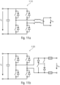
- the solution has some advantages over the prior art or the prior art has some disadvantages over the solution, e.g. B. that in all prior art topologies ( 11a, 11b , 11c, 11d ) the power semiconductors are switched on and off hard. Full-bridge or half-bridge inverter topologies can therefore achieve good efficiency at some operating points, but not over the entire operating range.
- NPC1 circuit Figure 11d , 1140
- NPC topology neutral point clamped circuit
- the internal switches are also operated at the fundamental frequency (the AC output voltage) to reduce the harmonics and reduce the switching losses, and the outer switch operated at higher switching frequency.
- the comparative example according to 3 can be expanded to include an energy sink, which is connected between the first output voltage connection 310 and the second output voltage connection 320 or between the first output voltage connection 310 and the input voltage supply line 340, so that a voltage at the energy sink has an AC voltage curve or an approximately mean-free AC voltage curve or a sinusoidal/cosinusoidal shape , means-free AC voltage curve corresponds.
- an arrangement can arise that corresponds to the circuit arrangement for generating an output AC voltage 200 2 can basically correspond.
- the reference potential node on the output side ie, for example, 350b of the 3
- the reference potential node 350a, 350b can therefore be designed as a node on the output side of the DC/DC converter 330 without an express possibility of making contact. This comment can be transferred to the other application examples.
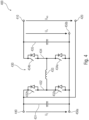
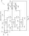
- FIG. 4 shows a schematic representation of a device for generating an AC voltage 400 with a "buck and step-up converter circuit” 430.
- the device for generating an AC voltage 400 has a first output voltage connection 410 and a second output voltage connection 420, for example by output voltage terminals, output voltage Plug contacts, output voltage screw connections, output voltage contacts or output voltage conductor tracks can be formed.
- An (output) AC voltage u WS can arise between the output voltage terminals 410, 420.
- the device for generating an AC voltage 400 has an input voltage feed 440 and a reference potential node 450a, 450b.
- the input voltage U E is applied between the input voltage supply 440 and the reference potential node 450a, 450b.
- the device for generating an AC voltage 400 has a “step-down and step-up converter circuit” 430 .
- this buck and boost converter 430 has an input capacitance 431 which is connected (coupled) between the input voltage feed 440 and the reference potential node 450a, 450b.
- the step-down and step-up converter 430 has a half-bridge circuit 432, which consists of two series-connected power switches 432a, 432b that are to be switched actively.
- Each of the two switches 432a, 432b of the half-bridge circuit 432 has an anti-parallel freewheeling diode.
- Active power switches can be, for example, metal-oxide-semiconductor field effect transistors (MOSFET) or bipolar transistors (BJT) or insulated gate bipolar transistors (IGBT).
- MOSFET metal-oxide-semiconductor field effect transistors
- BJT bipolar transistors
- IGBT insulated gate bipolar transistors
- the midpoint of the half-bridge circuit 432 is connected to a midpoint of a half-bridge circuit 434 via an inductance 433 (storage inductor, storage inductance).
- the half-bridge circuit 434 also has two power switches 434a, 434b that are to be switched actively.
- the two power switches 434a, 434b of the half-bridge circuit 434 each have an antiparallel freewheeling diode.
- the negative connection of the half-bridge circuit 434 is connected to the reference potential node 450a, 450b, the positive connection of the half-bridge circuit 434 is connected to connected to the output voltage terminal 410.
- An output capacitor 435 is connected in parallel with the half-bridge circuit 434 between the first output voltage connection 410 and the reference potential node 450a, 450b.
- the voltage u A ie the output voltage of the buck and boost converter 430, is present across this output capacitor 435.
- the device for generating an AC voltage 400 has an interconnection or a line connection that connects the input voltage feed 440 to the second output voltage connection 420 .
- the anodes of the freewheeling diodes (diodes, anti-parallel freewheeling diodes) of the low-lying power switches 432a, 434a of the half bridges 432, 434 are connected to the reference potential node 450a, 450b. With the power switch 432b high, the cathode of the diodes is connected to the input voltage supply 440 . The cathode of the diode of the high power switch 434b is connected to the positive terminal of the output capacitor 435 and the first output voltage terminal 410 .
- the cathodes of the diodes of the low-side switches 432a, 434a and the anodes of the diodes of the high-side switches 432b, 434b of a half-bridge 432, 434 are connected to one another and to the respective center point of a half-bridge 432, 434.
- the circuit Due to the soft-switching operation of the topology (e.g. with an input voltage of 400V and an output voltage of 200V...600V, the circuit generates a sinusoidal AC voltage of ⁇ 200V with the efficiency see Fig. 12b of DE102015219850 ) the switching losses are almost completely avoided.
- the output ground is not at 0 volts in relation to the reference potential node 450a, 450b, but at a constant potential and thus avoids displacement currents.
- the output voltage u A can be set in such a way that the output voltage shows a cosine-shaped potential curve which in turn has a mean value.
- This mean value can usefully be chosen to be the size of the input voltage U E , for example ⁇ 10%.
- a cosine/sine-shaped output voltage u WS between the first output voltage connection 410 and the second output voltage connection 420 can be achieved by this selection of the time curves.
- This sinusoidal potential course or the voltage curve can have a very low mean value, for example less than 10% of the amplitude of the sinusoidal potential curve (voltage curve).
- the device for generating an AC voltage 400 is suitable for supplying an AC voltage consumer with an (approximately) average-free AC voltage from a DC voltage source.
- a benefit can 4 be understood in a clear way. If the output voltage u A is considered, the counting direction of which is indicated by the corresponding arrow, it can be seen that the two antiparallel freewheeling diodes 434a, 434b of the half-bridge 434 are reverse-biased when the voltage is positive. With the same way of counting the output voltage u A but with a nominally negative voltage, the diodes 434a, 434b are forward-biased. Consequently, no significant negative voltage can be present across the output capacitor 435 . Thus, with a simple GS/GS converter 4 only one output voltage u A of one polarity can be generated.
- the second output voltage terminal 420 As a reference node for the AC output voltage, it is possible to generate a voltage that can be both positive and negative with respect to the second output voltage terminal 420 . Only then is it possible to generate an alternating voltage, ie a voltage with a positive and negative component. This possibility can also be transferred to the other comparative examples and exemplary embodiments.
- the comparative example according to 4 can be expanded to include an energy sink, which is connected between the first output voltage connection 410 and the second output voltage connection 420 or between the first output voltage connection 410 and the input voltage supply 440, so that a voltage at the energy sink has an AC voltage curve or an approximately mean-free AC voltage curve or a sinusoidal/cosinusoidal shape , means-free AC voltage curve corresponds.
- an arrangement can arise that corresponds to the circuit arrangement for generating an output AC voltage 200 2 can basically correspond.
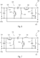
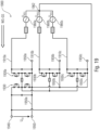
- figure 5 shows a schematic representation of a device for generating an AC voltage 500 with a "step-up and step-down converter circuit" 530.
- the device for generating an AC voltage 500 has a first output voltage connection 510 and a second output voltage connection 520, between which the AC voltage u WS is present .
- the device for generating an AC voltage 500 has an input voltage feed 540 and a reference potential node 550a, 550b.
- the input voltage U E is present between this reference potential node 550a, 550b and the input voltage supply line 540, which is therefore also present across the input capacitor 531.
- This input capacitor 531 is connected between the input voltage feed 540 and the reference potential node 550a, 550b.
- a coil 532 on the input side connects the positive terminal of the input capacitor 531 (i.e. also the input voltage supply 510) to the midpoint of a half-bridge circuit 533.
- the half-bridge circuit 533 in turn has two series-connected power switches 533a, 533b that are to be switched actively, each of which has an antiparallel freewheeling diode own.
- a capacitance 534 (coupling capacitor, intermediate storage capacitor) is connected in parallel with the half-bridge circuit 533 .
- a further half-bridge circuit 535 is connected in parallel with the coupling capacitor 534 .
- the half-bridge circuit 535 in turn also has two power switches 535a, 535b to be switched actively. Each of the power switches 535a, 535b to be switched actively in the half-bridge circuit 535 in turn has an antiparallel freewheeling diode.
- An output-side inductance 536 is connected to the middle point of the half-bridge circuit 535 , the second connection side of which is connected to a positive connection of an output capacitor 537 .
- This output capacitor 567 in turn is connected with the positive connection to the first output voltage connection 510 and with the negative connection to the reference potential node 550a, 550b.
- the reference potential node 550a, 550b connects the negative terminal of the input capacitor 531, the negative terminal of the half-bridge circuit 533, the negative terminal of the coupling capacitor 534, the negative terminal of the further half-bridge circuit 535 and the negative terminal of the output capacitor 537.
- the device for generating a AC voltage 500 an interconnection or line connection that connects the input voltage feed 540 to the second output voltage terminal 520 .
- the anodes of the freewheeling diodes (diodes, anti-parallel freewheeling diodes) of the low-lying power switches 533a, 535a of the half bridges 533, 535 are connected to the reference potential node 550a, 550b.
- the cathodes of the diodes are connected to the positive terminal of the coupling capacitance 534.
- the cathode of the diode of the low-side switch 533a and the anode of the diode of the high-side switch 533b are connected to one another and to the midpoint of the half-bridge 533 and to the second connection of the input-side inductance 532, respectively.
- the cathode of the diode of the low switch 535a and the anode of the diode of the high switch 535b are also connected to each other and to the midpoint of the half-bridge 535 and to the first terminal of the output-side inductor 536, respectively.
- the output voltage u A can be set in such a way that the output voltage u A in relation to the reference potential node 550a, 550b shows a cosine-shaped potential profile, which in turn has a mean value. It makes sense to select this mean value in the size of the input voltage U E .
- a sinusoidal output voltage u WS between the first output voltage connection 510 and the second output voltage connection 520 can be achieved by this choice of the time curves.
- This sinusoidal potential curve or voltage curve (related, for example, to the second output voltage connection 520) can have a very low mean value, for example less than 10% of the amplitude of the sinusoidal potential curve or voltage curve.
- the device for generating an AC voltage 500 is suitable for supplying an AC voltage consumer with an (approximately) average-free AC voltage from a DC voltage source.
- alternating voltage basically means a voltage that can have a positive and a negative polarity over time.
- the AC voltage can also be repeated periodically or averaged over one or more periods without an average value.
- the freedom from mean values can also only be approximately fulfilled, e.g. B. switching effects, control errors, etc. All the properties of the AC voltage mentioned can be transferred to the AC voltages of the other comparative examples and exemplary embodiments.
- the comparative example according to figure 5 can be expanded to include an energy sink, which is connected between the first output voltage connection 510 and the second output voltage connection 520 or between the first output voltage connection 510 and the input voltage supply line 540, so that a voltage at the energy sink has an AC voltage curve or an approximately mean-free AC voltage curve or a sinusoidal/cosinusoidal shape , means-free AC voltage curve corresponds.
- an arrangement can arise which can basically correspond to the circuit arrangement for generating an output AC voltage 200 .
- FIG. 6 shows a schematic representation of a device for generating an AC voltage 600 with an “unbalanced converter with input-side inductance circuit” 630 (English: “single ended primary inductance converter”, “SEPIC circuit”).
- the device for generating an AC voltage 600 with a "SEPIC circuit” 630 has a first output voltage connection 610 and a second output voltage connection 620 . The potential difference between these two connections is referred to as the output AC voltage or AC voltage u WS .
- the device for generating an AC voltage 600 has an input voltage feed 640 and a reference potential node 650a, 650b.
- the input voltage U E is present between the input voltage connections, ie the input voltage feed 640 and the reference potential node 650a, 650b.
- the device for generating an AC voltage 600 or the "SEPIC circuit” 630 has an input capacitor 631, which is connected between the input voltage feed 640 and the reference potential node 650a, 650b.
- the positive terminal of the input capacitor 631 is connected to an input inductor 632 .
- the second connection of the input inductance 632 is in turn connected to an active power switch 633 .
- This active power switch 633 has an antiparallel freewheeling diode (diode), the cathode of the diode of the power switch 633 is connected to the inductance 632 and the coupling capacitance 634 .
- the anode of the diode of the power switch 633 is connected to the reference potential node 650a, 650b.
- the negative connection of the active power switch 633 is connected to the reference potential node 650a, 650b.
- the positive connection of the active power switch 633 and the second connection of the input inductance 632 are connected to a coupling capacitance 634 (capacitor).
- This coupling capacitance 634 is in turn connected to the first connection of an inductance 635, whose second connection is in turn connected to the reference potential node 650a, 650b.
- the second connection of the coupling capacitance 634 and the first connection of the inductance 635 are in turn connected to an active power switch 636 .
- This active power switch 636 in turn has a diode (anti-parallel freewheeling diode).
- the anode of the diode of the power switch 636 is connected to the coupling capacitance 634 and the inductance 635 .
- the cathode of the power switch 636 is connected to the positive terminal of the output capacitor 637 and the output voltage terminal 610 .
- the second connection of the active power switch 636 is connected to a positive connection of an output capacitance 637 .
- the positive connection of the output capacitance 637 is connected to the active power switch 636 and the first output voltage connection 610, the negative connection of the output capacitance 637 is connected to the reference potential node 650a, 650b.
- the output voltage u A is present across this output capacitance 637 .
- the device for generating an AC voltage 600 has a connection/interconnection which connects the input voltage feed 640 to the second output voltage connection 620 .
- the output voltage u A which is present across the output capacitance 637, can be set to vary over time.
- a sinusoidal curve of the voltage (with a suitable mean value) across the output capacitance 637 it can be achieved that a sinusoidal, mean-free voltage curve (or approximately a mean-free voltage curve) is present between the terminals or connections 610, 620.
- an AC voltage u WS which is present between the first output voltage connection 610 and the second output voltage connection 620, can be generated from a DC voltage U E that is present between the input voltage supply 640 and the reference potential node 650a, 650b.
- a switching load reduction is possible for a switching load reduction to be achieved by suitable activation of the active power switches 633, 636 and/or by suitable switching load-relief interconnection of the active power switches 633, 636.
- This switching relief allows the circuit breakers to be switched on and off softly. This can improve the electromagnetic compatibility and/or the switching power loss.
- the comparative example according to 6 can be expanded to include an energy sink, which is connected between the first output voltage connection 610 and the second output voltage connection 620 or between the first output voltage connection 610 and the input voltage supply 640, so that a voltage at the energy sink has an AC voltage curve or an approximately mean-free AC voltage curve or a sinusoidal/cosinusoidal shape , means-free AC voltage curve corresponds.
- an arrangement can arise that corresponds to the circuit arrangement for generating an output AC voltage 200 2 can basically correspond.
- FIG. 7 shows a schematic representation of a device for generating an alternating voltage 700 with a "zeta circuit" 730.
- the so-called “zeta circuit” 730 corresponds to that in the comparative example 6 presented DC voltage / DC voltage converter circuit 630 related.
- the device for generating an AC voltage 700 has a first output voltage connection 710 and a second output voltage connection 720, via which the AC voltage or AC output voltage u WS is present. Furthermore, the device for generating an AC voltage 700 has an input voltage feed 740 and a reference potential node 750a, 750b.
- the input voltage U E is present between the input voltage connections, ie the input voltage feed 740 and the reference potential node 750a, 750b.
- the input capacitance 731 is connected between the input voltage feed 740 and the reference potential node 750a, 750b.
- the input voltage U E is in turn present across this input capacitance 731 .
- the positive connection of the input capacitance 731 is connected to a active power switch 732 connected, the negative terminal of the input capacitance 731 is connected to the reference potential node 750a, 750b.
- the active power switch 732 is connected to an inductance 733 and a coupling capacitance 734 at its second connection.
- the active power switch 732 includes a diode (anti-parallel freewheeling diode).
- the cathode of the diode of the power switch 732 is connected to the input capacitor 731 and the input voltage supply 740 .
- the anode of the diode power switch 732 is connected to the inductance 733 and the coupling capacitance 734 .
- the inductance 733 is connected at its first connection to the active power switch 732 and the first connection of the coupling capacitance 734 (coupling capacitor, capacitor).
- the second connection of the inductor 733 is connected to the reference potential node 750a, 750b.
- the second connection of the coupling capacitance 734 is in turn connected to an active power switch 735 and an inductance 736 .
- the negative connection of the active power switch 735 is connected to the reference potential node 750a, 750b and the power switch 735 has an associated diode (anti-parallel freewheeling diode).
- the cathode of the diode of the power switch 735 is connected to the coupling capacitance 734 and the first connection of the inductance 736, the anode of the associated diode of the power switch 735 is connected to the reference potential node 750a, 750b.
- the (output) inductance 736 is connected to the coupling capacitance 734 and the active power switch 735 at its first connection; the second connection of the inductance 736 is connected to the output capacitance 737 and the first output voltage connection 710 .
- the output capacitance 737 is in turn connected to the first output voltage connection 710 at its positive connection and to the reference potential node 750a, 750b at its negative connection.
- the output voltage u A is present across the output capacitance 737 .
- the device for generating an AC voltage 700 has an interconnection or a line connection or a conductor connection, which connects the input voltage feed 740 to the second output voltage connection 720 .
- the output voltage u A which is present across the output capacitance 737, can be set to vary over time.
- a sinusoidal waveform of the voltage across the output capacitance 737 can be achieved that a sinusoidal, mean value-free potential curve at the terminals 710, 720 is present.
- This can be achieved that from a DC voltage U E that is present between the input voltage supply 740 and the reference potential node 750a, 750b, an AC voltage u WS is generated that is present between the first output voltage terminal 710 and the second output voltage terminal 720.
- the comparative example 7 can be achieved by a suitable control of the active power switches 732, 735 that the output voltage u A assumes a sinusoidal curve.
- U E is the input voltage of the DC/DC converter.
- û is the amplitude of the sinusoidal voltage and satisfies the condition û ⁇ U E .
- the voltage difference between the output of the DC/DC converter, ie the voltage u A , and the input of the DC/DC converter, ie the voltage U E makes up the AC voltage u WS .
- the comparative example according to 7 be switched softly.
- the switching losses are almost completely avoided thanks to the soft-switching operation of the topology.
- Large voltage changes at the output are also reduced and thus harmonic loading (harmonic loading) is reduced.
- the output ground is not at 0V, but at a constant potential that approximately corresponds to the potential of the input voltage supply, thus avoiding displacement currents. If present, these displacement currents would have to be reduced by more complex filters.
- One advantage of the aforementioned devices for generating an AC voltage 100 to 700 is that the output mass remains at a constant voltage level and, as a result, unwanted displacement currents do not have to be reduced by expensive filters.
- a further advantage that all of the aforementioned devices for generating an AC voltage and the circuit arrangement for generating an output AC voltage 100 to 700 can have is that there are high voltage changes at the power semiconductors can be avoided and an associated high generation of harmonics. This low harmonic generation does not therefore have to be reduced by large output filters.
- the comparative example according to 7 can be expanded to include an energy sink, which is connected between the first output voltage connection 710 and the second output voltage connection 720 or between the first output voltage connection 710 and the input voltage supply line 740, so that a voltage at the energy sink has an AC voltage curve or an approximately mean-free AC voltage curve or a sinusoidal/cosinusoidal shape , means-free AC voltage curve corresponds.
- an arrangement can arise that corresponds to the circuit arrangement for generating an output AC voltage 200 2 can basically correspond.
- the method 800 includes operating 810 a DC-DC converter.
- an input voltage is present between an input voltage feed and a reference potential node.
- an output voltage of the DC-DC converter is generated in such a way that an output node at times has a potential that is more positive than the potential present at the input voltage supply.
- the DC-to-DC converters are operated in such a way that the output node temporarily has a potential which is more negative than the potential present at the input voltage supply.
- the method 800 further includes tapping 820 the AC output voltage for the energy sink between the output node and the input voltage supply.
- the output AC voltage is tapped 820 in such a way that the potential difference between the input voltage feed and the output node corresponds to a voltage present at the energy sink.
- This operating method 800 can also be used to generate an AC output voltage for an energy sink.
- This method can nevertheless be compared with the comparative examples Figures 1 to 7 presented devices for generating an AC voltage and circuit arrangements for generating an output AC voltage 100 - 700 are combined.
- the other comparative examples mentioned above can also be combined with the method for generating an alternating output voltage.
- the method can also be supplemented by the features and functionalities explained herein in relation to the devices according to the invention.
- FIG. 9 shows a schematic representation of an inverter 900 for generating an AC voltage from a DC voltage.
- the inverter has an input DC voltage connection 910, which is designed to have an input DC voltage applied to it.
- the DC voltage can originate, for example, from a DC voltage source, such as, for example, a plurality of photovoltaic cells (connected, for example, in series), a DC voltage energy store, or a rectified AC voltage.
- the inverter also has a device for generating an AC voltage 920, the device for generating an AC voltage 920 (e.g. as in the devices for generating an AC voltage 100, 300a, 400, 500, 600, 700, 1020) generating a DC voltage - DC/DC converters (e.g. such as DC/DC converters 130, 230, 330, 430, 530, 630, 730).
- the DC-DC converter may be configured to generate an output voltage based on an input voltage.
- the input voltage is present between an input voltage feed 922 and a reference potential node 924 .
- the DC voltage-DC voltage converter is designed to generate the output voltage in such a way that a first output voltage connection 926 temporarily has a potential that is more positive than the potential present at the input voltage feed 922 . Furthermore, the DC voltage-DC voltage converter is designed in such a way that the first output voltage connection 926 temporarily has a potential that is more negative than the potential present at the input voltage feed 922 . Furthermore, the second output voltage connection 928 is coupled to the input voltage feed 922 .
- the inverter 900 also has an AC output voltage connection 930 which is designed to provide an AC output voltage.
- the inverter is designed in such a way that the input voltage supply 922 and the reference potential node 924 of the device for generating an AC voltage 920 z. B. are coupled with low impedance to two contacts of the DC input voltage connection 910 . Furthermore, the first output voltage connection 926 and the second output voltage connection 928 of the device for generating an AC voltage 920 with contacts z. B. for connection of a load of the incoming AC voltage terminal 930 is coupled.
- the inverter 900 for generating an AC voltage from a DC voltage is thus designed to convert a DC voltage that is connected to the input DC voltage connection 910 into an output AC voltage that is provided at the output AC voltage connection 930 .
- An AC voltage load can thus be operated with the inverter 900 from a DC voltage source.
- This AC voltage load can represent a consumer, a load or possibly also an electrical supply network. In general, the AC voltage load can also be described by an energy sink.
- This system 900 can be equipped with the devices for generating an AC voltage and circuit arrangements for generating an output AC voltage, which are shown in the comparative examples according to Figures 1 to 7 were presented can be combined. Furthermore, the other aforementioned comparative examples presented in the summary of the invention can also be combined with the system 900. The system can otherwise be supplemented by the features and functionalities explained herein in relation to the devices according to the invention.
- FIG. 10 shows a schematic representation of an energy storage device 1000 for providing an AC voltage using a DC voltage energy store 1010, wherein the energy storage device 1000 has a DC voltage energy store 1010, which is designed to store energy and to provide the energy as DC voltage.
- a deviation of the DC voltage from a desired value can occur to a limited extent, for example when the energy is removed.
- the energy storage device 1000 has a device for generating an AC voltage 1020 (e.g. as in the devices for generating an AC voltage 100, 300a, 400, 500, 600, 700, 920).
- the device for generating an AC voltage 1020 has a DC-DC converter (z. B. like the GS / GS converter 130, 230, 330, 430, 530, 630, 730), which is designed to based on an input voltage, for example the DC voltage provided by the DC voltage energy storage source 1010, to generate an output voltage, the input voltage being present between an input voltage feed 1022 and a reference potential node 1024.
- a DC-DC converter z. B. like the GS / GS converter 130, 230, 330, 430, 530, 630, 730
- the DC voltage-DC voltage converter is designed to generate the output voltage in such a way that a first output voltage connection 1026 temporarily has a potential that is more positive than the potential present at the input voltage feed 1022 . Furthermore, the DC-DC converter is designed to generate the output voltage in such a way that the first output voltage connection 1026 temporarily has a potential that is more negative than the potential present at the input voltage feed 1022 . Furthermore, the second output voltage connection 1028 is coupled to the input voltage feed 1022, for example directly, statically, in a low-impedance, low-impedance, low-inductance manner.
- the energy storage device 1000 has an output AC voltage connection 1030 which is designed to provide an output AC voltage.
- the DC energy storage device 1010 is included in the energy storage device 1000 the input voltage supply 1022 and the reference potential node 1024 of the device for generating an AC voltage 1020 coupled.
- This energy storage device or energy storage connection 1000 can be used, for example, in the field of hybrid/electric vehicles.
- the direct voltage energy store 1010 can be implemented, for example, by a chemical direct voltage energy source such as an accumulator.
- a chemical direct voltage energy source such as an accumulator.
- DC voltage energy stores are also conceivable, which can deliver stored energy in the form of DC voltage.
- the DC voltage energy store can release the stored energy, which can be stored, for example, in chemical form or as rotational energy, in the form of electrical energy or in the form of electrical power over a period of time.
- the electrical voltage can only deviate to a negligible extent from a mean voltage, for example within a high-frequency period of the GS/GS converter or a few high-frequency periods of the GS/GS converter.
- the energy source can thus be viewed as an approximately constant voltage source or direct voltage source or direct voltage energy store.
- This system 1000 can be equipped with the devices for generating an AC voltage and circuit arrangements for generating an output AC voltage, which are shown in the comparative examples according to FIG Figures 1 to 7 were presented can be combined. Furthermore, the other aforementioned comparative examples presented in the summary of the invention can also be combined with the system 100. The system can also be supplemented by the features and functionalities explained herein in relation to the devices according to the invention.
- the exemplary embodiment shows a possible embodiment of a three-phase inverter that is based on the solution according to the invention.
- FIG. 12 12 shows an illustration of a three-phase inverter 1200 according to a comparative example.
- the suffixes a, b, c assign the respective elements to one of the three phases, which can thus be referred to as phase a, phase b and phase c.
- the three-phase inverter 1200 has three DC/DC converters 1230a, 1230b, 1230c.
- An input voltage supply 1240a, 1240b, 1240c is assigned to each of these GS/GS converters 1230a, 1230b, 1230c.
- These input voltage feeds 1240a, 1240b, 1240c are connected together to form the (superordinate) input voltage feed 1240.
- the three-phase inverter 1200 has three reference potential nodes 1250a, 1250b, 1250c. These reference potential nodes 1250a, 1250b, 1250c can also be combined with the (superordinate) reference potential node 1250 to form a "large" reference potential node. In order to point out the lack of galvanic isolation of the GS/GS converters 1230a, 1230b, 1230c, the reference potential nodes are also shown on the “output side” of the GS/GS converters 1230a, 1230b, 1230c as the reference potential nodes 1250a, 1250b, 1250c.
- the GS/GS converters 1230a, 1230b, 1230c are designed, for example, such that they provide a positive output voltage (related to the respective reference potential node 1250a, 1250b, 1250c) at the output node 1210a, 1210b, 1210c in a respective first time segment and so that they provide a negative output voltage (related to the respective reference potential node 1250a, 1250b, 1250c) at the output node 1210a, 1210b, 1210c in a respective second period of time.
- a load 1260a, 1260b, 1260c is connected between the respective output nodes 1210a, 1210b, 1210c and a neutral point 1262 (or thus between the respective output nodes 1210a, 1210b, 1210c and the input voltage supply 1240).
- This load can generally be an energy sink, too a three-phase network would be conceivable at this point, or a three-phase motor.
- the z. B. in relation to the comparative example according to 2 and the energy sink 260 have been named.
- the connections of the three-phase energy sink 1260a, 1260b, 1260c can, for example, be brought together on one connection side in a star point 1262, which in turn is coupled to the input voltage feed 1240.
- multiple single-phase energy sinks can also be separately coupled to the (superordinate) input voltage supply 1240 . It would also be possible to couple these to the input voltage leads 1240a, 1240b, 1240c.
- the step-up and step-down function can in turn be achieved by suitable control of the GS/GS converters 1230a, 1230b, 1230c.
- suitable control of the GS/GS converters 1230a, 1230b, 1230c e.g. B. also a phase-shifted control of the GS / GS converter 1230a, 1230b, 1230c be useful.
- a three-phase inverter 1300 is shown, which has a comparable structure to the inverter 1200.
- a respective "general" GS/GS converter 1230a, 1230b, 1230c was replaced by a “concrete” example of a “buck and boost converter circuit” 1330a, 1330b, 1330c, the other topologies of the aforementioned (single-phase) comparative examples (such as e.g., the "boost and buck circuit", the "SEPIC circuit”, etc.) can also be used.
- the input voltage leads 1340, 1340a, 1340b, 1340c and the reference potential nodes 1350, 1350a, 1350b, 1350c are designed analogously to the inverter 1200, for example.
- the energy sink 1360a, 1360b, 1360c corresponds to the energy sink 1260a, 1260b, 1260c.
- the star point 1362 also corresponds in principle to the star point 1262.
- the fact that the energy sink 1360a, 1360b, 1360c is connected between a respective output node 1310a, 1310b, 1310c and the input voltage supply 1340 is again important. This makes it possible to convert the DC voltage that is present between the input voltage supply 1340 and the reference potential node 1350 into a (three-phase) AC voltage that is (approximately) present at the respective phases of the energy sink 1360a, 1360b, 1360c.
- the inverter 1400 has an arrangement similar to that of the comparative example 13 can be derived.
- the phase of the energy sink 1460a, 1460b, 1460c is connected between a respective output node 1410a, 1410b, 1410c and the input voltage supply 1440, as in the previous comparative examples.
- a sinusoidal AC voltage which also has, for example, a phase offset between the respective AC voltages, advantageously z. B. has a phase shift of 120 °.
- the GS/GS converters can be formed from a combination of a front (input-side) circuit part 1330 with the three rear (output-side) circuit parts 1330a, 1330b, 1330c.
- the inductances 1333a, 1333b, 1333c (coils, chokes) can also have a decoupling function between the three phases.
- a clocking or a clocking frequency of the front circuit part 1330 can also be selected to be significantly higher than a clocking of the three rear circuit parts 1330a, 1330b, 1330c.
- a clock frequency of the front circuit part 1330 can be selected which corresponds approximately to three times the clock frequency of the three rear circuit parts 1330a, 1330b, 1330c.
- the front circuit part 1330 can be used, for example, as a buck converter and that the three rear circuit parts 1330a, 1330b, 1330c z. B. can be used as a step-up converter.
- the three rear circuit parts 1330a, 1330b, 1330c z. B. can be used as a step-up converter.
- other functionalities would also be conceivable, which can be achieved, for example, by a suitable control or selection of the component values.
- energy sinks (1260a, 1260b, 1260c; 1360a, 1360b, 1360c; 1460a, 1460b, 1460c) are shown as components. These energy sinks can be dispensable functionally and thus represent only one example of a possible embodiment. Accordingly derived from this would be conceivable, which have no energy sinks, but instead provide a three-phase AC voltage system (e.g. a symmetrical, three-phase AC voltage system (AC system), e.g. with a phase offset of 120°) at several connection terminals.
- the connection terminals can have different designs. For example, screw connections or plug-in connections or clamp connections or also a mechanical connection and electrical contacting, which is implemented by different devices in each case, would be conceivable.
- the coupling can thus also be realized by one of the other GS-GS converters, but this should advantageously be formed in such a way that the neutral point (or a corresponding connection or corresponding connections of the (three-phase) energy sink) has a potential which is approximately the potential corresponds to the input voltage supply.
- Figure 15a Figures 16a and 16b show three different comparative examples. All clarify the concept of using the solution according to the invention for rectifying an AC voltage.
- Figure 15b shows the (schematic, exemplary) time curves of three voltages, which also illustrate the concept of using the solution according to the invention as a rectifier circuit.
- Figure 15a shows a representation of a circuit for generating a DC voltage 1500a from an AC voltage source 1515, the circuit z. B. with the circuit 300a in 3 is comparable.
- the circuit for generating a DC voltage 1500a has an AC voltage feed 1510, 1520, which is formed by the two terminals (contacts or the like), the first (input) AC voltage terminal 1510 and the second (input) AC voltage terminal 1520.
- These contacts/connections/terminals can be formed in different ways. Screw, clamp, plug-in connections can be just as conceivable as crimped connections. It can be said in general terms that, in addition to electrical contacting, mechanical attachment is usually desired. The actual execution can be very different.
- the AC voltage supply 1510, 1520 is supplied with a sinusoidal AC voltage, for example, which is symbolized by an AC voltage source 1515.
- This (input) AC voltage can have a mean value that is not equal to zero.
- the circuit for generating an AC voltage 1500a has a DC-DC converter 1530 (GS/GS converter, DC/DC converter).
- This GS-GS converter 1530 can be designed in such a way that it generates a DC voltage between a first (output) DC voltage connection 1540 and a second (output) DC voltage connection 1550, with the GS-GS converter 1530 being designed in such a way that this generates the magnitude of the DC voltage U GS , for example, in such a way that it approximately corresponds to the mean value of the (input) AC voltage 1515 .
- the difference to the aforementioned comparative examples, which generate an AC voltage from a DC voltage is the energy flow direction.
- the power flow direction (energy flow direction) is according to the comparative example Figure 15a viewed from right to left and indicated with an arrow labeled WS/GS. With the solution, it may thus be possible to set an energy flow direction, ie to use the same embodiment of the solution for rectification and also for inversion.
- Figure 15b shows a schematic representation 1500b of the time course of the three voltages u WS 1572, U GS+ 1574 and U Gs- 1576.
- the representation 1500b has an abscissa 1570, which represents a time axis, and also an ordinate 1571, which represents a voltage axis.
- the representation 1500b shows the three voltages, the (input) AC voltage 1572 ( u WS ), the positive (output) DC voltage 1574 (or the positive (output) potential) ( U GS+ ) and the negative output DC voltage 1576 (or the negative (output) potential) ( U GS- ).
- the concept of the solution according to the invention can thus be understood from the time curves.
- a potential of the AC voltage u WS for example the potential of the second AC voltage connection 1520, is coupled to the first (output) DC voltage connection 1540.
- the potential of the AC voltage u WS selected for this can advantageously be such that the potential has an approximately static (time-invariant, fixed, fixed) potential ( u GS+ ) with respect to an (electrical) mass or with respect to earth.
- the GS-GS converter 1530 is designed in such a way that it converts the (time-varying) potential present at the first AC voltage connection 1510 in such a way that the second output DC voltage connection 1550, which can correspond to a reference potential node 1550 of the GS-GS converter 1530, has an approximately time-invariant potential ( u GS- ).
- a DC voltage U GS can thus be made available between the first output DC voltage connection 1540 and the second output DC voltage connection 1550 .
- the time course of the AC voltage u WS 1572 is sinusoidal and (relative to the potential U GS- ) has a mean value which is not equal to zero.
- the time profile of the (output DC) voltage (or the potential) U GS+ 1574 is approximately constant (related to the potential U GS- ) and corresponds (approximately) to the mean value of the AC voltage u WS .
- the time course of the potential u GS- is also (approximately) constant in the representation and is shown as (approximately) zero. This results in the output DC voltage U GS .
- This output DC voltage is therefore the potential difference between U GS+ and U GS- .
- a DC output voltage can thus be generated from an AC voltage source using the solution according to the invention.
- the circuit 1500 can also be understood in such a way that the DC voltage-DC voltage converter 1530 generates or regulates a voltage U GS between the first input voltage connection 1540 and the second input voltage connection 1550 .
- a first connection of the AC voltage source 1515 to the first AC voltage connection 1510 and by connecting a second connection of the AC voltage source 1515 to the second AC voltage connection 1520 it can be achieved (for example by suitable dimensioning) that in stationary operation of the circuit 1500a the Potential at the first AC voltage connection is always positive (in other embodiments always negative) compared to the potential at the second output DC voltage connection, i.e. it does not cross the "reference potential" of the DC voltage-DC voltage converter".
- Input voltage of the DC-DC converter related to the reference potential of the DC-DC converter (i.e. related to the potential of the potential rail, which is connected to both the input circuit of the DC-DC converter and the output circuit of the DC-DC converter with low resistance coupled), never to zero.
- the DC voltage-DC voltage converter can receive an input voltage which differs from zero at any point in time (for example during an entire period of the AC voltage).
- the DC-DC converter can achieve power transmission at all times (for example, during an entire cycle of the AC voltage).
- Figures 16a and 16b show two further comparative examples, also for generating a DC voltage U GS from an AC voltage source 1615a, 1615b.
- the solution is implemented with a "step-down and step-up converter circuit".
- the circuit for generating a DC voltage 1600a from an AC voltage source 1615a has a first AC voltage connection 1610a and a second AC voltage connection 1620a.
- the AC voltage source 1615a is connected to these AC voltage contacts 1610a, 1620a, or the circuit for generating a DC voltage 1600a can be supplied with an AC voltage ( u WS ) via the AC voltage terminals 1610a, 1620a.
- one terminal of the AC voltage source 1615a is coupled to the first AC voltage terminal 1610a.
- Another connection of the AC voltage source 1615a is coupled to the second AC voltage connection 1620a.
- This second AC voltage connection 1620a is in turn coupled to the first (output) DC voltage connection 1640a.
- This can e.g. B. statically, directly, happen with low resistance. It is important that the coupling is implemented in such a way that the potential of the coupled connection of the AC voltage source 1615a approximately corresponds to the potential of the first (output) DC voltage connection 1640a.
- the circuit for generating a DC voltage 1600a has a GS-GS converter 1630a, which corresponds to a “buck and boost converter circuit” in the comparative example shown.
- This first output DC voltage connection is separated from the continuous reference potential or reference potential node of the DC voltage-DC voltage converter or is connected to the continuous reference potential of the DC voltage-DC voltage converter via one or more switches not directly connected. Rather, a reference potential node of the DC-DC converter 1630a may correspond to the second (output) DC voltage terminal 1650a.
- This can, for example, have a fixed potential that does not change over time, which is denoted by U GS- in the illustration.
- a direct voltage U GS is thus made available with the potential of the first (output) direct voltage connection 1640a U GS+ .
- This DC voltage U GS thus corresponds to a potential difference between the two (output) DC voltage connections 1640a, 1650a.
- the GS/GS converter 1630a can be designed in such a way that the GS/GS converter 1630a has no galvanic isolation, or that at least the power-transmitting part has no galvanic isolation (input circuit and output circuit are both low-impedance to the reference potential node tied together).
- the circuit 1600a has a first input AC voltage connection 1610a and an "explicit" second input AC voltage connection 1620a, which in turn has e.g. B. can be connected to a line with the first output DC voltage terminal 1640a.
- the AC voltage source 1615b is connected between two nodes (or a node and a terminal). On one side to a first input AC voltage node 1610b and on the other side to the node of the first output DC voltage connection (or to the output DC voltage connection 1540b).
- the two different comparative examples are based on the idea of the solution according to the invention.
- the power flow direction is selected from an AC voltage source 1615a, 1615b to a (possible) DC voltage consumer, while in the corresponding comparative example 400 a power flow direction is selected from a DC voltage source to a (possible) AC voltage load.
- the solution according to the invention thus permits both functionalities.
- This direction of power flow is indicated by an arrow labeled WS-GS.
- the comparative example is a device for generating a DC voltage 1500, 1600a from an input AC voltage.
- the DC voltage is present between a first output DC voltage connection 1540, 1640a and a second output DC voltage connection 1550, 1650a.
- the device has a DC voltage-DC voltage converter 1530, 1630a, which is designed to generate the DC voltage based on a first potential of the input AC voltage and on a potential of the second output DC voltage connection 1550, 1650a (or based on the time-varying potential difference).
- the first potential of the AC input voltage is present at a first AC input voltage terminal 1510, 1610a
- the second potential of the AC input voltage is present at a second AC input voltage terminal 1520, 1620a.
- the DC voltage-DC voltage converter 1530, 1630a is also designed to generate the DC voltage in such a way that the first output DC voltage connection 1540, 1640a has a potential which is approximately constant in relation to the second output DC voltage connection 1550, 1650a.
- the second input AC voltage connection 1520, 1620a is coupled to the first output DC voltage connection 1540, 1640a.
- the comparative example of the circuit arrangement for generating a DC output voltage 1600b from an AC voltage source 1615b has a first DC output voltage connection 1640b and a second DC output voltage connection 1650b, between which the DC output voltage is present. Furthermore, the circuit arrangement for generating an output DC voltage has a DC voltage-DC voltage converter 1630b.
- the DC voltage-DC voltage converter 1630b is designed to generate the output DC voltage based on a first potential of the AC voltage source 1615b and a potential of the second output DC voltage connection 1650b.
- the DC voltage-DC voltage converter 1630b is designed to generate the output DC voltage in such a way that the first output DC voltage connection 1640b has a potential which is approximately constant in relation to the second output DC voltage connection 1650b. Furthermore, the first potential of the AC voltage source 1615b is present at an input AC voltage node 1610b and a second potential of the AC voltage source 1615b is present at the first output DC voltage connection 1640b, so that the potential difference between the first output DC voltage connection 1640b and the input AC voltage node 1610b corresponds to a voltage output by the AC voltage source 1615b.
- An approximately constant potential can mean, for example, a maximum deviation of 5% from the mean value of the potential (or the voltage or the potential difference).
- 17 , 18 and 19 show comparative examples and an exemplary embodiment of the solution according to the invention for generating a DC voltage from a three-phase AC voltage (for example a three-phase AC voltage system, or also a symmetrical, three-phase AC voltage system).
- the circuit for generating a DC voltage 1700 from a three-phase AC voltage can be used as in 17 shown.
- the circuit for generating a DC voltage 1700 can be viewed as being divided into three phases or circuit paths, or the circuit for generating a DC voltage 1700 can be made up of three single-phase rectifiers, such as e.g. Am 15 or 16 shown, put together.
- the three phases a, b and c are structured in a way that is comparable to one another.
- the (three-phase) AC voltage source 1760a, 1760b, 1760c is connected at its three phases to the corresponding (input) AC voltage terminals 1710a, 1710b, 1710c of the DC/DC converters 1730a, 1730b, 1730c.
- the three phases of the three-phase AC voltage source are brought together at a star point 1762 on their other connection side.
- the neutral point 1762 is coupled to a first (output) DC voltage connection 1740 .
- a controller and/or regulator can be designed such that the potential of the star point 1762 approximately corresponds to the potential of the first output DC voltage connection 1740 .
- the output DC voltage U GS is made available.
- the direction of energy flow is indicated by the arrow labeled WS/GS.
- This energy flow direction is not solely predetermined by the circuit, but can be a consequence of the (three-phase) AC voltage source 1760a, 1760b, 1760c. If the AC voltage source 1760a, 1760b, 1760c is replaced by a (three-phase) load and if a DC voltage is applied to the (output) DC voltage connections 1740, 1750 (e.g. by a DC voltage source), the circuit can also be used as a (three-phase) inverter .
- a three-phase rectifier 1800 is shown, e.g. B. can be based on the concept of the three-phase rectifier 1700.
- the GS-GS converters 1830a, 1830b, 1830c are constructed as "buck and boost converter circuits". Many elements of rectifier 1700 can be found in rectifier 1800.
- a three-phase AC voltage source 1860a, 1860b, 1860c provides a three-phase (symmetrical) AC voltage system (eg with a phase offset between the individual phases of 120°).
- the respective first connection side of the three phases of the three-phase AC voltage source 1860a, 1860b, 1860c is coupled to a respective first (input) AC voltage connection 1810a, 1810b, 1810c of the GS/GS converter 1830a, 1830b, 1830c.
- the second connection sides of the three phases of the three-phase AC voltage source 1860a, 1860b, 1860c are connected to form a star point 1862.
- the star point 1862 is coupled to a first output DC voltage connection 1840, or to a respective first (output) DC voltage connection 1840a, 1840b, 1840c of the GS/GS converters 1830a, 1830b, 1830c.
- the reference potential nodes 1850a, 1850b, 1850c of the GS/GS converters 1830a, 1830b, 1830c are also coupled or connected to one another and form a common reference potential node 1850, which can also be the second (output) DC voltage connection 1850, for example.
- a connection of the star point 1862 to the first (output) AC voltage connection 1840 can be omitted in a symmetrical AC voltage system of the three-phase AC voltage source 1860a, 1860b, 1860c.
- the coupling of the star point 1862 (or the three-phase AC voltage sources 1860a 1860b, 1860c) to the first (output) DC voltage connection 1840 can be realized through one of the phases. Nevertheless, it can be advantageous that the potential of the star point 1862 corresponds approximately to the potential of the first output DC voltage connection 1840.
- a three-phase rectifier 1900 is shown.
- This three-phase rectifier 1900 has a number of similarities with the three-phase rectifier 1700 and the three-phase rectifier 1800. All three rectifiers are powered by a three-phase AC power source (in 19 : the three-phase AC voltage source 1960a, 1960b, 1960c). Furthermore, there are the correspondences of the first (input) AC voltage connections 1910a, 1910b, 1910c, the star point 1962, the first (output) DC voltage connection 1940 and the second (output) DC voltage connection 1950.
- the second output DC voltage connection 1950 can be connected to a reference potential node of a ( or more) DC-DC converters 1930, 1930a, 1930b, 1930c.
- the GS/GS converters 1930, 1930a, 1930b, 1930c of the GS-GS converters cannot be "concretely” identified herein as a "classic”"buck and boost converter circuit". become. Nevertheless, the GS-GS converters 1930, 1930a, 1930b, 1930c (or combinations of the GS/GS converters) should be able to master step-up and step-down conversion in order to convert a desired DC voltage, for example at the level of an average value of the AC voltage at the (output) To provide direct voltage connections in 1940, 1950.
- the rectifier circuit 1900 can enable a power flow direction from an AC voltage source to a DC voltage load, but also from a DC voltage source to an AC voltage load.
- the power flow direction is sensibly from the source to a (possible) load specified.
- the load can be connected to the DC output terminals 1940, 1950 and thus be supplied by an AC (three-phase) voltage source 1960a, 1960b, 1960c.
- a three-phase rectifier device for generating a DC voltage 1700, 1800, 1900 which is between a first output DC voltage connection 1740, 1740a, 1740b, 1740c, 1840, 1840a, 1840b, 1840c, 1940, 1940a, 1940b, 1940c and a second output DC voltage terminal 1750, 1750a, 1750b, 1750c, 1850, 1850a, 1850b, 1850c, 1950, 1950a, 1950b, 1950c can be created.
- the three-phase rectifier device 1700, 1800, 1900 has a plurality of DC-DC converters 1730a, 1730b, 1730c, 1830a, 1830b, 1830c, 1930, 1930a, 1930b, 1930c, which are designed to based on a first potential of a respective Phase of a three-phase AC voltage and a potential of the second output DC voltage terminal 1750, 1750a, 1750b, 1750c, 1850, 1850a, 1850b, 1850c, 1950, 1950a, 1950b, 1950c to generate a respective output voltage.
- the first potential of the respective phase of the three-phase AC voltage is at a respective input AC voltage connection 1710a, 1710b, 1710c, 1810a, 1810b, 1810c, 1910a, 1910b, 1910c and a second potential of the respective phase of the three-phase AC voltage is at a neutral point 1762, 1862, 1962 at.
- the DC-DC converters 1730a, 1730b, 1730c, 1830a, 1830b, 1830c, 1930, 1930a, 1930b, 1930c are designed to generate the respective output voltage in such a way that the first output DC voltage connection 1740, 1740a, 1740b, 1740 c, 1840, 1840a, 1840b, 1840c, 1940, 1940a, 1940b, 1940c with respect to the second DC output terminal 1750, 1750a, 1750b, 1750c, 1850, 1850a, 1850b, 1850c, 1950, 1950a , 1950b, 1950c has a potential that (at least in a steady state operation) is approximately constant.
- star point 1762, 1862, 1962 is coupled to the first output DC voltage terminal 1740, 1740a, 1740b, 1740c, 1840, 1840a, 1840b, 1840c, 1940, 1940a, 1940b, 1940c.
- This exemplary embodiment shows a further possible configuration of the solution according to the invention; another configuration is explained below.
- a three-phase rectifier circuit for generating an output DC voltage 1700, 1800 1900 between a first output DC voltage terminal 1740, 1740a, 1740b, 1740c, 1840, 1840a, 1840b, 1840c, 1940, 1940a, 1940 b, 1940c and a second DC output terminal 1750, 1750a, 1750b, 1750c, 1850, 1850a, 1850b, 1850c, 1950, 1950a, 1950b, 1950c from a three-phase AC voltage source 1760a, 1760b, 1760c, 186 0a, 1860b, 1860c, 1960a, 1960b, 1960c to provided.
- the three-phase rectifier circuit 1700, 1800, 1900 has a plurality of DC-DC converters 1730a, 1730b, 1730c, 1830a, 1830b, 1830c, 1930, 1930a, 1930b, 1930s, which are designed to based on a first potential of a respective Phase of the three-phase AC voltage source 1760a, 1760b, 1760c, 1860a, 1860b, 1860c, 1960a, 1960b, 1960c and a potential of the respective second output DC voltage connection 1750, 1750a, 1750b, 1750c, 1850, 1850a, 1850b, 1850c, 1950, 1950a, 1950b, 1950c to generate a respective output voltage.
- the DC-DC converters 1730a, 1730b, 1730c, 1830a, 1830b, 1830c, 1930, 1930a, 1930b, 1930c are designed to generate the respective output voltage in such a way that the respective first output DC voltage terminal 1740, 1740a, 1740b, 174 0c, 1840 , 1840a, 1840b, 1840c, 1940, 1940a, 1940b, 1940c in relation to the respective second output DC voltage terminal 1750, 1750a, 1750b, 1750c, 1850, 1850a, 1850b, 1850c, 1950, 19 50a, 1950b, 1950c has a potential which ( at least in steady state operation, ie after the end of a start-up phase) is approximately constant.
- the three-phase AC voltage sources 1760a, 1760b, 1760c, 1860a, 1860b, 1860c, 1960a, 1960b, 1960c are connected to the first output DC voltage connection 1740, 1740a, 1740b, 1740c, 1840, 1840a, 184 0b, 1840c, 1940, 1940a, 1940b, 1940c coupled , so that the potential difference between a respective input AC voltage node 1710a, 1710b, 1710c, 1810a, 1810b, 1810c, 1910a, 1910b, 1910c and the respective first output DC voltage terminal 1740, 1740a, 1740b, 1740c, 1840, 1840a , 1840b, 1840c, 1940, 1940a, 1940b, 1940c corresponds to a voltage output by the respective phase of the three-phase AC voltage source 1760a, 1760b, 1760c, 1860a, 1860b, 1860c, 1960a, 1960b, 1960c.
- An approximately constant potential can mean, for example, a maximum deviation of 5% from the mean value of the potential (or the voltage or the potential difference).
Landscapes
- Engineering & Computer Science (AREA)
- Power Engineering (AREA)
- Transportation (AREA)
- Mechanical Engineering (AREA)
- Dc-Dc Converters (AREA)
- Inverter Devices (AREA)
Claims (6)
- Dispositif onduleur triphasé (1400) pour générer un système de tension alternative triphasée qui est présent entre plusieurs premières connexions de tension de sortie (1410a; 1410b; 1410c) et un point neutre (1462), aux caractéristiques suivantes:trois convertisseurs de tension continue-tension continue (1430; 1430a; 1430b; 1430c) qui sont configurés pour générer, sur base d'une tension d'entrée, une tension de sortie respective; etdans lequel la tension d'entrée est présente entre une alimentation en tension d'entrée (1440) et un noeud de potentiel de référence (1450; 1450a; 1450b; 1450c); etdans lequel les convertisseurs de tension continue-tension continue (1430; 1430a; 1430b; 1430c) sont conçus pour générer la tension de sortie respective de sorte que la première connexion de tension de sortie respective (1410a; 1410b; 1410c) présente temporairement un potentiel qui est plus positif que le potentiel présent sur l'alimentation en tension d'entrée (1440), et pour la générer de sorte que la première connexion de tension de sortie respective (1410a; 1410b; 1410c) présente temporairement un potentiel qui est plus négatif que le potentiel présent sur l'alimentation en tension d'entrée (1440); etdans lequel le point neutre (1462) est couplé à l'alimentation en tension d'entrée (1440);dans lequel le premier convertisseur de tension continue-tension continue présente un circuit abaisseur et élévateur de tension;dans lequel le circuit abaisseur et élévateur de tension présente un premier circuit en demi-pont (1430), qui est connecté entre l'alimentation en tension d'entrée (1440) et le noeud de potentiel de référence (1450), et qui présente deux interrupteurs de puissance connectés en série à commuter activement, où chacun des interrupteurs du premier circuit en demi-pont présente une diode de roue libre antiparallèle,dans lequel un point central du premier circuit en demi-pont (1430) est connecté à un point central d'un deuxième circuit en demi-pont (1430a) par l'intermédiaire d'une première inductance (1433a),dans lequel le deuxième circuit en demi-pont (1430a) présente deux interrupteurs de puissance à commuter activement,dans lequel les interrupteurs de puissance du deuxième circuit en demi-pont (1430a) présentent, chacun, une diode de roue libre antiparallèle,dans lequel une connexion négative du deuxième circuit en demi-pont (1430a) est connectée au noeud de potentiel de référence (1450), etdans lequel une connexion positive du deuxième circuit en demi-pont (1430a) est connectée à la première connexion de tension de sortie (1410a) du premier convertisseur de tension continue-tension continue (1430, 1430a);dans lequel le deuxième convertisseur de tension continue-tension continue (1430, 1430b) présente un troisième circuit en demi-pont (1430b),dans lequel un point central du troisième circuit en demi-pont (1430b) est connecté au point central du premier circuit en demi-pont (1430) par l'intermédiaire d'une deuxième inductance (1433b),dans lequel une connexion négative du troisième circuit en demi-pont (1430b) est connectée au noeud de potentiel de référence (1450),dans lequel une connexion positive du troisième circuit en demi-pont est connectée à la première connexion de tension de sortie (1410b) du deuxième convertisseur de tension continue-tension continue (1430, 1430b);dans lequel le troisième convertisseur de tension continue-tension continue (1430, 1430c) présente un quatrième circuit en demi-pont (1430c),dans lequel un point central du quatrième circuit en demi-pont (1430c) est connecté au point central du premier circuit en demi-pont (1430) par l'intermédiaire d'une inductance (1433c),dans lequel une connexion négative du quatrième circuit en demi-pont (1430c) est connectée au noeud de potentiel de référence (1450),dans lequel une connexion positive du quatrième circuit en demi-pont (1430c) est connectée à la première connexion de tension de sortie du troisième convertisseur de tension continue-tension continue (1430, 1430c),dans lequel le dispositif onduleur triphasé est conçu pour fournir un système de tension alternative triphasé aux connexions de tension de sortie.
- Dispositif onduleur triphasé (1400) selon la revendication 1,
dans lequel une fréquence d'horloge de la partie de circuit (1430) du côté de l'entrée est sélectionnée supérieure à une fréquence d'horloge des trois parties de circuit (1430a, 1430b, 1430c) du côté de la sortie. - Dispositif onduleur triphasé (1400) selon l'une des revendications 1 à 2,
dans lequel le dispositif onduleur triphasé est conçu pour fournir un système de tension alternative triphasé symétrique avec un déphasage de 120 degrés aux connexions de tension de sortie. - Dispositif onduleur triphasé (1400) selon l'une des revendications 1 à 3,
dans lequel le dispositif onduleur triphasé est conçu pour fournir une tension alternative sinusoïdale aux connexions de tension de sortie. - Dispositif onduleur triphasé (1400) selon l'une des revendications 1 à 4,dans lequel les convertisseurs de tension continue-tension continue (1430; 1430a; 1430b; 1430c) sont conçus pour générer la tension de sortie respective de sorte queune valeur moyenne d'une courbe de potentiel respective à une connexion de tension de sortie respective diffère d'un potentiel à l'alimentation en tension d'entrée de tout au plus 10% de la tension d'entrée,et pour la générer de sorte qu'une amplitude d'une courbe de potentiel à une connexion de tension de sortie respective soit d'au moins 30% d'une valeur de la tension d'entrée,et pour la générer de sorte qu'une connexion de tension de sortie respective présente une courbe de potentiel sans moyenne variable dans le temps et se répétant périodiquement par rapport à l'alimentation en tension d'entrée,et pour la générer de sorte qu'il existe un déphasage entre les tensions de sortie respectives.
- Circuit redresseur triphasé (1900) pour générer une tension continue de sortie (UGS) qui est présente entre une première connexion de tension continue de sortie (1940) et une deuxième connexion de tension continue de sortie (1950), à partir d'une source de tension alternative triphasée (1960a; 1960b; 1960c), aux caractéristiques suivantes:trois convertisseurs de tension continue-tension continue (1930; 1930a; 1930b; 1930c) qui sont conçus pour générer, sur base d'une différence de potentiel entre un premier potentiel d'une phase respective de la source de tension alternative triphasée (1960a; 1960b; 1960c) et un potentiel de la deuxième connexion de tension continue de sortie (1950), une tension de sortie (UGS); etdans lequel les convertisseurs de tension continue-tension continue (1930; 1930a; 1930b; 1930c) sont conçus pour générer la tension de sortie de sorte que la première connexion de tension continue de sortie (1940) présente, par rapport à la deuxième connexion de tension continue de sortie (1950), un potentiel qui est approximativement constant; etdans lequel la source de tension alternative triphasée (1960a; 1960b; 1960c) est couplée à la première connexion de tension continue de sortie (1940) de sorte que la différence de potentiel entre un noeud de tension alternative d'entrée respectif (1910a; 1910b; 1910c) et la première connexion de tension continue de sortie (1940) corresponde à une tension délivrée par la phase respective de la source de tension alternative triphasée (1960a; 1960b; 1960c);dans lequel le premier convertisseur de tension continu-tension continu (1930, 1930a) présente un circuit abaisseur et élévateur de tension;dans lequel le circuit abaisseur et élévateur abaisseur présente un premier circuit en demi-pont (1930a) qui est connecté entre un premier noeud de tension alternative d'entrée (1910a) et la deuxième connexion de tension continue de sortie (1950), où chacun des interrupteurs du premier circuit en demi-pont (1930a) présente respectivement une diode de roue libre antiparallèle,dans lequel un point central du premier circuit en demi-pont (1930a) est connecté à un point central d'un deuxième circuit en demi-pont (1930) par l'intermédiaire d'une inductance,dans lequel les interrupteurs de puissance du deuxième circuit en demi-pont (1930) présentent, chacun, une diode de roue libre antiparallèle,dans lequel une connexion négative du deuxième circuit en demi-pont (1930) est connectée à la deuxième connexion de tension continue de sortie (1950), etdans lequel une connexion positive du deuxième circuit en demi-pont (1930) est connectée à la première connexion de tension continue de sortie (1940);dans lequel le deuxième convertisseur de tension continue-tension continue (1930, 1930b) présente un troisième circuit en demi-pont (1930b) qui est connecté entre un deuxième noeud de tension alternative d'entrée (1910b) et la deuxième connexion de tension continue de sortie (1950), dans lequel chacun des interrupteurs du troisième circuit en demi-pont (1930b) présente respectivement une diode de roue libre antiparallèle,dans lequel un point central du troisième circuit en demi-pont (1930b) est connecté au point central du deuxième circuit en demi-pont (1930) par l'intermédiaire d'une deuxième inductance,dans lequel une connexion négative du troisième circuit en demi-pont (1930b) est connectée à la deuxième connexion de tension continue de sortie (1950),dans lequel le troisième convertisseur de tension continue-tension continue (1930, 1930c) présente un quatrième circuit en demi-pont (1930c) qui est connecté entre un troisième noeud de tension alternative d'entrée (1910c) et la deuxième connexion de tension continue de sortie (1950), dans lequel chacun des interrupteurs du quatrième circuit en demi-pont (1930c) présente respectivement une diode de roue libre antiparallèle;dans lequel un point central du quatrième circuit en demi-pont (1930c) est connecté au point central du deuxième circuit en demi-pont (1930) par l'intermédiaire d'une inductance,dans lequel une connexion négative du quatrième circuit en demi-pont (1930c) est connectée à la deuxième connexion de tension continue de sortie (1950).
Applications Claiming Priority (2)
| Application Number | Priority Date | Filing Date | Title |
|---|---|---|---|
| DE102016207941.7A DE102016207941A1 (de) | 2016-05-09 | 2016-05-09 | Vorrichtung zur Erzeugung einer Wechselspannung, Schaltungsanordnung zur Erzeugung einer Ausgangswechselspannung, Verfahren zur Erzeugung einer Ausgangswechselspannung für eine Energiesenke, Wechselrichter zur Erzeugung einer Wechselspannung aus einer Gleichspannung, Energiespeicher-Vorrichtung zur Bereitstellung einer Wechselspannung unter Verwendung eines Gleichspannungsenergiespeichers, dreiphasige Wechselrichtervorrichtung, dreiphasige Wechselrichterschaltung, und Konzept zur Erzeugung einer Gleichspannung |
| PCT/EP2017/060938 WO2017194477A1 (fr) | 2016-05-09 | 2017-05-08 | Dispositif et procédé pour produire une tension alternative |
Publications (2)
| Publication Number | Publication Date |
|---|---|
| EP3455932A1 EP3455932A1 (fr) | 2019-03-20 |
| EP3455932B1 true EP3455932B1 (fr) | 2023-07-19 |
Family
ID=58671706
Family Applications (1)
| Application Number | Title | Priority Date | Filing Date |
|---|---|---|---|
| EP17721721.3A Active EP3455932B1 (fr) | 2016-05-09 | 2017-05-08 | Dispositif et procédé pour produire une tension alternative |
Country Status (3)
| Country | Link |
|---|---|
| EP (1) | EP3455932B1 (fr) |
| DE (1) | DE102016207941A1 (fr) |
| WO (1) | WO2017194477A1 (fr) |
Families Citing this family (1)
| Publication number | Priority date | Publication date | Assignee | Title |
|---|---|---|---|---|
| DE102018116486A1 (de) | 2018-07-06 | 2020-01-09 | HELLA GmbH & Co. KGaA | Kopplungsvorrichtung |
Citations (11)
| Publication number | Priority date | Publication date | Assignee | Title |
|---|---|---|---|---|
| EP1168593A2 (fr) * | 2000-06-26 | 2002-01-02 | Toyota Jidosha Kabushiki Kaisha | Appareil pour production d'énergie mécanique et onduleur |
| DE102005024465A1 (de) * | 2005-05-24 | 2006-11-30 | Hantschel, Jochen, Dipl.-Ing. (FH) | Schaltungsanordnung und Steuerungsverfahren für einen Umrichter |
| DE102005015658A1 (de) * | 2005-04-06 | 2007-01-11 | Bayerische Motoren Werke Ag | Schalteinrichtung zur Verknüpfung verschiedener elektrischer Spannungsebenen in einem Kraftfahrzeug |
| EP2048774A2 (fr) * | 2007-10-10 | 2009-04-15 | Denso Corporation | Système électrique rotatif avec enroulements de stator multiphase connectés en étoile |
| US20100019705A1 (en) * | 2008-07-28 | 2010-01-28 | Denso Corporation | Electric power conversion circuit, and control device for multiphase electric rotary machine |
| CH699364B1 (de) * | 2006-07-27 | 2010-02-26 | Eth Zuerich Eth Transfer | Drehstromantriebssystem mit motorintegriertem Hochfrequenztrafo zur bidirektionalen Kopplung der Versorgungsspannungen |
| WO2010051812A1 (fr) * | 2008-11-07 | 2010-05-14 | Danfoss Solar Inverters A/S | Centrale photovoltaïque possédant une source de tension de décalage commandant le potentiel de courant continu à la sortie de l’inverseur |
| US20140078802A1 (en) * | 2012-09-14 | 2014-03-20 | Ziya Ozkan | Dc/ac inverter to convert dc current/voltage to ac current/voltage |
| CN203674732U (zh) * | 2014-01-02 | 2014-06-25 | 艾伏新能源科技(上海)股份有限公司 | T型三电平三相四桥臂光伏并网发电系统 |
| US20140334213A1 (en) * | 2013-05-08 | 2014-11-13 | Abb Oy | Switching arrangement for inverter, and inverter |
| WO2015193003A1 (fr) * | 2014-06-20 | 2015-12-23 | Robert Bosch Gmbh | Élévateur/réducteur de tension utilisé comme déphaseur pour machine électrique |
Family Cites Families (6)
| Publication number | Priority date | Publication date | Assignee | Title |
|---|---|---|---|---|
| JP4196867B2 (ja) * | 2004-03-31 | 2008-12-17 | 株式会社デンソー | 双方向昇降圧型チョッパ回路及びそれを用いたインバータ回路並びにdc−dcコンバータ回路 |
| JP2006223008A (ja) * | 2005-02-08 | 2006-08-24 | Hitachi Ltd | Dc−dcコンバータ |
| JP5278298B2 (ja) * | 2009-12-17 | 2013-09-04 | 株式会社デンソー | 電力変換回路の制御装置 |
| WO2014004575A1 (fr) * | 2012-06-25 | 2014-01-03 | Arizona Board Of Regents, For And On Behalf Of Arizona State University | Circuits et procédés pour des onduleurs photovoltaïques |
| DE102013113000A1 (de) * | 2013-11-25 | 2015-05-28 | Sma Solar Technology Ag | Verfahren zum Betreiben eines Wechselrichters und Wechselrichter mit einem Schalter zwischen einem Mittelpunkt eines Gleichspannungszwischenkreises und einem Anschluss für einen Nullleiter eines Wechselstromnetzes |
| DE102015219850A1 (de) | 2015-10-13 | 2017-04-13 | Fraunhofer-Gesellschaft zur Förderung der angewandten Forschung e.V. | Vorrichtung zum Steuern eines schaltenden Gleichspannungswandlers, schaltender Gleichspannungswandler und Verfahren zum Steuern eines geschalteten Gleichspannungswandlers |
-
2016
- 2016-05-09 DE DE102016207941.7A patent/DE102016207941A1/de not_active Ceased
-
2017
- 2017-05-08 WO PCT/EP2017/060938 patent/WO2017194477A1/fr not_active Ceased
- 2017-05-08 EP EP17721721.3A patent/EP3455932B1/fr active Active
Patent Citations (11)
| Publication number | Priority date | Publication date | Assignee | Title |
|---|---|---|---|---|
| EP1168593A2 (fr) * | 2000-06-26 | 2002-01-02 | Toyota Jidosha Kabushiki Kaisha | Appareil pour production d'énergie mécanique et onduleur |
| DE102005015658A1 (de) * | 2005-04-06 | 2007-01-11 | Bayerische Motoren Werke Ag | Schalteinrichtung zur Verknüpfung verschiedener elektrischer Spannungsebenen in einem Kraftfahrzeug |
| DE102005024465A1 (de) * | 2005-05-24 | 2006-11-30 | Hantschel, Jochen, Dipl.-Ing. (FH) | Schaltungsanordnung und Steuerungsverfahren für einen Umrichter |
| CH699364B1 (de) * | 2006-07-27 | 2010-02-26 | Eth Zuerich Eth Transfer | Drehstromantriebssystem mit motorintegriertem Hochfrequenztrafo zur bidirektionalen Kopplung der Versorgungsspannungen |
| EP2048774A2 (fr) * | 2007-10-10 | 2009-04-15 | Denso Corporation | Système électrique rotatif avec enroulements de stator multiphase connectés en étoile |
| US20100019705A1 (en) * | 2008-07-28 | 2010-01-28 | Denso Corporation | Electric power conversion circuit, and control device for multiphase electric rotary machine |
| WO2010051812A1 (fr) * | 2008-11-07 | 2010-05-14 | Danfoss Solar Inverters A/S | Centrale photovoltaïque possédant une source de tension de décalage commandant le potentiel de courant continu à la sortie de l’inverseur |
| US20140078802A1 (en) * | 2012-09-14 | 2014-03-20 | Ziya Ozkan | Dc/ac inverter to convert dc current/voltage to ac current/voltage |
| US20140334213A1 (en) * | 2013-05-08 | 2014-11-13 | Abb Oy | Switching arrangement for inverter, and inverter |
| CN203674732U (zh) * | 2014-01-02 | 2014-06-25 | 艾伏新能源科技(上海)股份有限公司 | T型三电平三相四桥臂光伏并网发电系统 |
| WO2015193003A1 (fr) * | 2014-06-20 | 2015-12-23 | Robert Bosch Gmbh | Élévateur/réducteur de tension utilisé comme déphaseur pour machine électrique |
Non-Patent Citations (1)
| Title |
|---|
| MYRZIK JOHANNA: "Topologische Untersuchungen zur Anwendung von tief- hochsetzenden Stellern für Wechselrichter", TOPOLOGISCHE UNTERSUCHUNGEN ZUR ANWENDUNG VON TIEF-, HOCHSETZENDEN STELLERN FÜR WECHSELRICHTER, KASSEL UNIV. PRESS, KASSEL, 1 January 2001 (2001-01-01), pages 1 - 175, XP008103662, ISBN: 978-3-933146-62-5 * |
Also Published As
| Publication number | Publication date |
|---|---|
| EP3455932A1 (fr) | 2019-03-20 |
| WO2017194477A1 (fr) | 2017-11-16 |
| DE102016207941A1 (de) | 2017-11-09 |
Similar Documents
| Publication | Publication Date | Title |
|---|---|---|
| EP2432109B1 (fr) | Commutateur modulaire pour un convertisseur électrique, convertisseur électrique et procédé de fonctionnement d'un convertisseur électrique | |
| EP3496259B1 (fr) | Système de convertisseur électrique | |
| DE102016218304B3 (de) | Vorrichtung zur Spannungswandlung, Traktionsnetz und Verfahren zum Laden einer Batterie | |
| EP2237404B1 (fr) | Onduleur avec deux ponts asymmetrics et une branche à roue libre découplante l'entrée du courant continu de la sortie du courant alternatif | |
| DE102011005184B4 (de) | Leistungshalbleiterbauelement und dieses verwendendes Leistungsumformungssystem | |
| EP2107672A1 (fr) | Onduleur triphasé sans connexion entre le conducteur de neutre du réseau et le point milieu du circuit intermédiaire | |
| DE102019106485B4 (de) | Weissach-Gleichrichteranordnung | |
| DE102013005070B4 (de) | Hoch-Tiefsetzsteller | |
| EP3005543A1 (fr) | Transducteur dc/dc multi-niveaux modulaire pour applications hvdc | |
| DE102017212462A1 (de) | Galvanisch gekoppelter elektrischer Wandler | |
| EP2992595A1 (fr) | Ensemble mutateur à mutateurs multi-étages câblés en parallèle et son procédé de commande | |
| DE102010060508B4 (de) | Spannungswandler mit einer Speicherdrossel mit einer Wicklung und einer Speicherdrossel mit zwei Wicklungen | |
| EP2928060A1 (fr) | Circuit de convertisseur modulaire doté de sous-modules présentant différentes capacités de commutation | |
| EP2845303A1 (fr) | Convertisseur et procédés de conversion de tension | |
| WO2009156021A1 (fr) | Circuit transformateur de tension et onduleur | |
| DE102014101571B4 (de) | Wechselrichter sowie verfahren zum betrieb eines wechselrichters | |
| DE102013224511B4 (de) | Elektrisches Antriebssystem mit Ladeschaltung für eine Energiespeichereinrichtung und Verfahren zum Betreiben einer Energiespeichereinrichtung | |
| EP3455932B1 (fr) | Dispositif et procédé pour produire une tension alternative | |
| DE102016201283A1 (de) | Wechselrichter, elektrische Antriebsanordnung mit einem Wechselrichter | |
| WO2022101396A1 (fr) | Dispositif de conversion de mode commun faible de tension alternative | |
| WO2009098093A2 (fr) | Ensemble onduleur permettant l'injection d'énergie produite par voie photovoltaïque dans un réseau public | |
| DE102014203404A1 (de) | Stromrichterschaltung und Verfahren zum Betreiben derselben | |
| WO2018172329A1 (fr) | Onduleur | |
| DE102018209139B4 (de) | Wechselspannungs-Ladevorrichtung | |
| DE102014005124A1 (de) | Schaltungsanordnung und Verfahren zum Austausch elektrischer Energie |
Legal Events
| Date | Code | Title | Description |
|---|---|---|---|
| STAA | Information on the status of an ep patent application or granted ep patent |
Free format text: STATUS: UNKNOWN |
|
| STAA | Information on the status of an ep patent application or granted ep patent |
Free format text: STATUS: THE INTERNATIONAL PUBLICATION HAS BEEN MADE |
|
| PUAI | Public reference made under article 153(3) epc to a published international application that has entered the european phase |
Free format text: ORIGINAL CODE: 0009012 |
|
| STAA | Information on the status of an ep patent application or granted ep patent |
Free format text: STATUS: REQUEST FOR EXAMINATION WAS MADE |
|
| 17P | Request for examination filed |
Effective date: 20181108 |
|
| AK | Designated contracting states |
Kind code of ref document: A1 Designated state(s): AL AT BE BG CH CY CZ DE DK EE ES FI FR GB GR HR HU IE IS IT LI LT LU LV MC MK MT NL NO PL PT RO RS SE SI SK SM TR |
|
| AX | Request for extension of the european patent |
Extension state: BA ME |
|
| DAV | Request for validation of the european patent (deleted) | ||
| DAX | Request for extension of the european patent (deleted) | ||
| STAA | Information on the status of an ep patent application or granted ep patent |
Free format text: STATUS: EXAMINATION IS IN PROGRESS |
|
| 17Q | First examination report despatched |
Effective date: 20210112 |
|
| RAP3 | Party data changed (applicant data changed or rights of an application transferred) |
Owner name: HOCHSCHULE FUER ANGEWANDTE WISSENSCHAFTEN HAMBURG Owner name: FRAUNHOFER-GESELLSCHAFT ZUR FOERDERUNG DER ANGEWANDTEN FORSCHUNG E.V. |
|
| GRAP | Despatch of communication of intention to grant a patent |
Free format text: ORIGINAL CODE: EPIDOSNIGR1 |
|
| STAA | Information on the status of an ep patent application or granted ep patent |
Free format text: STATUS: GRANT OF PATENT IS INTENDED |
|
| RIC1 | Information provided on ipc code assigned before grant |
Ipc: B60L 15/00 19680901ALI20221231BHEP Ipc: H02M 7/48 19680901ALI20221231BHEP Ipc: H02M 3/155 19740701ALI20221231BHEP Ipc: H02M 7/537 19740701ALI20221231BHEP Ipc: H02M 3/158 19850101AFI20221231BHEP |
|
| INTG | Intention to grant announced |
Effective date: 20230202 |
|
| GRAS | Grant fee paid |
Free format text: ORIGINAL CODE: EPIDOSNIGR3 |
|
| GRAA | (expected) grant |
Free format text: ORIGINAL CODE: 0009210 |
|
| STAA | Information on the status of an ep patent application or granted ep patent |
Free format text: STATUS: THE PATENT HAS BEEN GRANTED |
|
| AK | Designated contracting states |
Kind code of ref document: B1 Designated state(s): AL AT BE BG CH CY CZ DE DK EE ES FI FR GB GR HR HU IE IS IT LI LT LU LV MC MK MT NL NO PL PT RO RS SE SI SK SM TR |
|
| REG | Reference to a national code |
Ref country code: GB Ref legal event code: FG4D Free format text: NOT ENGLISH |
|
| REG | Reference to a national code |
Ref country code: CH Ref legal event code: EP |
|
| REG | Reference to a national code |
Ref country code: DE Ref legal event code: R096 Ref document number: 502017015074 Country of ref document: DE |
|
| REG | Reference to a national code |
Ref country code: IE Ref legal event code: FG4D Free format text: LANGUAGE OF EP DOCUMENT: GERMAN |
|
| REG | Reference to a national code |
Ref country code: LT Ref legal event code: MG9D |
|
| REG | Reference to a national code |
Ref country code: NL Ref legal event code: MP Effective date: 20230719 |
|
| PG25 | Lapsed in a contracting state [announced via postgrant information from national office to epo] |
Ref country code: NL Free format text: LAPSE BECAUSE OF FAILURE TO SUBMIT A TRANSLATION OF THE DESCRIPTION OR TO PAY THE FEE WITHIN THE PRESCRIBED TIME-LIMIT Effective date: 20230719 |
|
| PG25 | Lapsed in a contracting state [announced via postgrant information from national office to epo] |
Ref country code: GR Free format text: LAPSE BECAUSE OF FAILURE TO SUBMIT A TRANSLATION OF THE DESCRIPTION OR TO PAY THE FEE WITHIN THE PRESCRIBED TIME-LIMIT Effective date: 20231020 |
|
| PG25 | Lapsed in a contracting state [announced via postgrant information from national office to epo] |
Ref country code: IS Free format text: LAPSE BECAUSE OF FAILURE TO SUBMIT A TRANSLATION OF THE DESCRIPTION OR TO PAY THE FEE WITHIN THE PRESCRIBED TIME-LIMIT Effective date: 20231119 |
|
| PG25 | Lapsed in a contracting state [announced via postgrant information from national office to epo] |
Ref country code: SE Free format text: LAPSE BECAUSE OF FAILURE TO SUBMIT A TRANSLATION OF THE DESCRIPTION OR TO PAY THE FEE WITHIN THE PRESCRIBED TIME-LIMIT Effective date: 20230719 Ref country code: RS Free format text: LAPSE BECAUSE OF FAILURE TO SUBMIT A TRANSLATION OF THE DESCRIPTION OR TO PAY THE FEE WITHIN THE PRESCRIBED TIME-LIMIT Effective date: 20230719 Ref country code: PT Free format text: LAPSE BECAUSE OF FAILURE TO SUBMIT A TRANSLATION OF THE DESCRIPTION OR TO PAY THE FEE WITHIN THE PRESCRIBED TIME-LIMIT Effective date: 20231120 Ref country code: NO Free format text: LAPSE BECAUSE OF FAILURE TO SUBMIT A TRANSLATION OF THE DESCRIPTION OR TO PAY THE FEE WITHIN THE PRESCRIBED TIME-LIMIT Effective date: 20231019 Ref country code: LV Free format text: LAPSE BECAUSE OF FAILURE TO SUBMIT A TRANSLATION OF THE DESCRIPTION OR TO PAY THE FEE WITHIN THE PRESCRIBED TIME-LIMIT Effective date: 20230719 Ref country code: LT Free format text: LAPSE BECAUSE OF FAILURE TO SUBMIT A TRANSLATION OF THE DESCRIPTION OR TO PAY THE FEE WITHIN THE PRESCRIBED TIME-LIMIT Effective date: 20230719 Ref country code: IS Free format text: LAPSE BECAUSE OF FAILURE TO SUBMIT A TRANSLATION OF THE DESCRIPTION OR TO PAY THE FEE WITHIN THE PRESCRIBED TIME-LIMIT Effective date: 20231119 Ref country code: HR Free format text: LAPSE BECAUSE OF FAILURE TO SUBMIT A TRANSLATION OF THE DESCRIPTION OR TO PAY THE FEE WITHIN THE PRESCRIBED TIME-LIMIT Effective date: 20230719 Ref country code: GR Free format text: LAPSE BECAUSE OF FAILURE TO SUBMIT A TRANSLATION OF THE DESCRIPTION OR TO PAY THE FEE WITHIN THE PRESCRIBED TIME-LIMIT Effective date: 20231020 Ref country code: FI Free format text: LAPSE BECAUSE OF FAILURE TO SUBMIT A TRANSLATION OF THE DESCRIPTION OR TO PAY THE FEE WITHIN THE PRESCRIBED TIME-LIMIT Effective date: 20230719 |
|
| PG25 | Lapsed in a contracting state [announced via postgrant information from national office to epo] |
Ref country code: PL Free format text: LAPSE BECAUSE OF FAILURE TO SUBMIT A TRANSLATION OF THE DESCRIPTION OR TO PAY THE FEE WITHIN THE PRESCRIBED TIME-LIMIT Effective date: 20230719 |
|
| REG | Reference to a national code |
Ref country code: DE Ref legal event code: R097 Ref document number: 502017015074 Country of ref document: DE |
|
| PG25 | Lapsed in a contracting state [announced via postgrant information from national office to epo] |
Ref country code: ES Free format text: LAPSE BECAUSE OF FAILURE TO SUBMIT A TRANSLATION OF THE DESCRIPTION OR TO PAY THE FEE WITHIN THE PRESCRIBED TIME-LIMIT Effective date: 20230719 |
|
| PG25 | Lapsed in a contracting state [announced via postgrant information from national office to epo] |
Ref country code: SM Free format text: LAPSE BECAUSE OF FAILURE TO SUBMIT A TRANSLATION OF THE DESCRIPTION OR TO PAY THE FEE WITHIN THE PRESCRIBED TIME-LIMIT Effective date: 20230719 Ref country code: RO Free format text: LAPSE BECAUSE OF FAILURE TO SUBMIT A TRANSLATION OF THE DESCRIPTION OR TO PAY THE FEE WITHIN THE PRESCRIBED TIME-LIMIT Effective date: 20230719 Ref country code: ES Free format text: LAPSE BECAUSE OF FAILURE TO SUBMIT A TRANSLATION OF THE DESCRIPTION OR TO PAY THE FEE WITHIN THE PRESCRIBED TIME-LIMIT Effective date: 20230719 Ref country code: EE Free format text: LAPSE BECAUSE OF FAILURE TO SUBMIT A TRANSLATION OF THE DESCRIPTION OR TO PAY THE FEE WITHIN THE PRESCRIBED TIME-LIMIT Effective date: 20230719 Ref country code: DK Free format text: LAPSE BECAUSE OF FAILURE TO SUBMIT A TRANSLATION OF THE DESCRIPTION OR TO PAY THE FEE WITHIN THE PRESCRIBED TIME-LIMIT Effective date: 20230719 Ref country code: CZ Free format text: LAPSE BECAUSE OF FAILURE TO SUBMIT A TRANSLATION OF THE DESCRIPTION OR TO PAY THE FEE WITHIN THE PRESCRIBED TIME-LIMIT Effective date: 20230719 Ref country code: SK Free format text: LAPSE BECAUSE OF FAILURE TO SUBMIT A TRANSLATION OF THE DESCRIPTION OR TO PAY THE FEE WITHIN THE PRESCRIBED TIME-LIMIT Effective date: 20230719 |
|
| PLBE | No opposition filed within time limit |
Free format text: ORIGINAL CODE: 0009261 |
|
| STAA | Information on the status of an ep patent application or granted ep patent |
Free format text: STATUS: NO OPPOSITION FILED WITHIN TIME LIMIT |
|
| 26N | No opposition filed |
Effective date: 20240422 |
|
| PG25 | Lapsed in a contracting state [announced via postgrant information from national office to epo] |
Ref country code: SI Free format text: LAPSE BECAUSE OF FAILURE TO SUBMIT A TRANSLATION OF THE DESCRIPTION OR TO PAY THE FEE WITHIN THE PRESCRIBED TIME-LIMIT Effective date: 20230719 |
|
| PG25 | Lapsed in a contracting state [announced via postgrant information from national office to epo] |
Ref country code: BG Free format text: LAPSE BECAUSE OF FAILURE TO SUBMIT A TRANSLATION OF THE DESCRIPTION OR TO PAY THE FEE WITHIN THE PRESCRIBED TIME-LIMIT Effective date: 20230719 |
|
| PG25 | Lapsed in a contracting state [announced via postgrant information from national office to epo] |
Ref country code: BG Free format text: LAPSE BECAUSE OF FAILURE TO SUBMIT A TRANSLATION OF THE DESCRIPTION OR TO PAY THE FEE WITHIN THE PRESCRIBED TIME-LIMIT Effective date: 20230719 |
|
| REG | Reference to a national code |
Ref country code: CH Ref legal event code: PL |
|
| PG25 | Lapsed in a contracting state [announced via postgrant information from national office to epo] |
Ref country code: MC Free format text: LAPSE BECAUSE OF FAILURE TO SUBMIT A TRANSLATION OF THE DESCRIPTION OR TO PAY THE FEE WITHIN THE PRESCRIBED TIME-LIMIT Effective date: 20230719 |
|
| PG25 | Lapsed in a contracting state [announced via postgrant information from national office to epo] |
Ref country code: LU Free format text: LAPSE BECAUSE OF NON-PAYMENT OF DUE FEES Effective date: 20240508 |
|
| GBPC | Gb: european patent ceased through non-payment of renewal fee |
Effective date: 20240508 |
|
| PG25 | Lapsed in a contracting state [announced via postgrant information from national office to epo] |
Ref country code: MC Free format text: LAPSE BECAUSE OF FAILURE TO SUBMIT A TRANSLATION OF THE DESCRIPTION OR TO PAY THE FEE WITHIN THE PRESCRIBED TIME-LIMIT Effective date: 20230719 Ref country code: LU Free format text: LAPSE BECAUSE OF NON-PAYMENT OF DUE FEES Effective date: 20240508 Ref country code: CH Free format text: LAPSE BECAUSE OF NON-PAYMENT OF DUE FEES Effective date: 20240531 |
|
| REG | Reference to a national code |
Ref country code: BE Ref legal event code: MM Effective date: 20240531 |
|
| PG25 | Lapsed in a contracting state [announced via postgrant information from national office to epo] |
Ref country code: IE Free format text: LAPSE BECAUSE OF NON-PAYMENT OF DUE FEES Effective date: 20240508 |
|
| PG25 | Lapsed in a contracting state [announced via postgrant information from national office to epo] |
Ref country code: BE Free format text: LAPSE BECAUSE OF NON-PAYMENT OF DUE FEES Effective date: 20240531 |
|
| PG25 | Lapsed in a contracting state [announced via postgrant information from national office to epo] |
Ref country code: GB Free format text: LAPSE BECAUSE OF NON-PAYMENT OF DUE FEES Effective date: 20240508 |
|
| PGFP | Annual fee paid to national office [announced via postgrant information from national office to epo] |
Ref country code: DE Payment date: 20250519 Year of fee payment: 9 |
|
| PGFP | Annual fee paid to national office [announced via postgrant information from national office to epo] |
Ref country code: IT Payment date: 20250530 Year of fee payment: 9 |
|
| REG | Reference to a national code |
Ref country code: AT Ref legal event code: MM01 Ref document number: 1590481 Country of ref document: AT Kind code of ref document: T Effective date: 20240508 |
|
| PGFP | Annual fee paid to national office [announced via postgrant information from national office to epo] |
Ref country code: FR Payment date: 20250523 Year of fee payment: 9 |
|
| PG25 | Lapsed in a contracting state [announced via postgrant information from national office to epo] |
Ref country code: AT Free format text: LAPSE BECAUSE OF NON-PAYMENT OF DUE FEES Effective date: 20240508 |
|
| PG25 | Lapsed in a contracting state [announced via postgrant information from national office to epo] |
Ref country code: CY Free format text: LAPSE BECAUSE OF FAILURE TO SUBMIT A TRANSLATION OF THE DESCRIPTION OR TO PAY THE FEE WITHIN THE PRESCRIBED TIME-LIMIT; INVALID AB INITIO Effective date: 20170508 |
|
| PG25 | Lapsed in a contracting state [announced via postgrant information from national office to epo] |
Ref country code: HU Free format text: LAPSE BECAUSE OF FAILURE TO SUBMIT A TRANSLATION OF THE DESCRIPTION OR TO PAY THE FEE WITHIN THE PRESCRIBED TIME-LIMIT; INVALID AB INITIO Effective date: 20170508 |