EP3470681A1 - Traverse électrique pour appareil à vide, sous la forme d'une plaque de circuit imprimé - Google Patents
Traverse électrique pour appareil à vide, sous la forme d'une plaque de circuit imprimé Download PDFInfo
- Publication number
- EP3470681A1 EP3470681A1 EP17195789.7A EP17195789A EP3470681A1 EP 3470681 A1 EP3470681 A1 EP 3470681A1 EP 17195789 A EP17195789 A EP 17195789A EP 3470681 A1 EP3470681 A1 EP 3470681A1
- Authority
- EP
- European Patent Office
- Prior art keywords
- board
- conductor
- vacuum
- layer
- vacuum apparatus
- Prior art date
- Legal status (The legal status is an assumption and is not a legal conclusion. Google has not performed a legal analysis and makes no representation as to the accuracy of the status listed.)
- Granted
Links
Images


Classifications
-
- F—MECHANICAL ENGINEERING; LIGHTING; HEATING; WEAPONS; BLASTING
- F04—POSITIVE - DISPLACEMENT MACHINES FOR LIQUIDS; PUMPS FOR LIQUIDS OR ELASTIC FLUIDS
- F04D—NON-POSITIVE-DISPLACEMENT PUMPS
- F04D25/00—Pumping installations or systems
- F04D25/02—Units comprising pumps and their driving means
- F04D25/06—Units comprising pumps and their driving means the pump being electrically driven
- F04D25/0693—Details or arrangements of the wiring
-
- F—MECHANICAL ENGINEERING; LIGHTING; HEATING; WEAPONS; BLASTING
- F04—POSITIVE - DISPLACEMENT MACHINES FOR LIQUIDS; PUMPS FOR LIQUIDS OR ELASTIC FLUIDS
- F04D—NON-POSITIVE-DISPLACEMENT PUMPS
- F04D19/00—Axial-flow pumps
- F04D19/02—Multi-stage pumps
- F04D19/04—Multi-stage pumps specially adapted to the production of a high vacuum, e.g. molecular pumps
-
- F—MECHANICAL ENGINEERING; LIGHTING; HEATING; WEAPONS; BLASTING
- F04—POSITIVE - DISPLACEMENT MACHINES FOR LIQUIDS; PUMPS FOR LIQUIDS OR ELASTIC FLUIDS
- F04D—NON-POSITIVE-DISPLACEMENT PUMPS
- F04D29/00—Details, component parts, or accessories
- F04D29/02—Selection of particular materials
- F04D29/023—Selection of particular materials especially adapted for elastic fluid pumps
-
- F—MECHANICAL ENGINEERING; LIGHTING; HEATING; WEAPONS; BLASTING
- F04—POSITIVE - DISPLACEMENT MACHINES FOR LIQUIDS; PUMPS FOR LIQUIDS OR ELASTIC FLUIDS
- F04D—NON-POSITIVE-DISPLACEMENT PUMPS
- F04D29/00—Details, component parts, or accessories
- F04D29/08—Sealings
- F04D29/083—Sealings especially adapted for elastic fluid pumps
-
- H—ELECTRICITY
- H05—ELECTRIC TECHNIQUES NOT OTHERWISE PROVIDED FOR
- H05K—PRINTED CIRCUITS; CASINGS OR CONSTRUCTIONAL DETAILS OF ELECTRIC APPARATUS; MANUFACTURE OF ASSEMBLAGES OF ELECTRICAL COMPONENTS
- H05K1/00—Printed circuits
- H05K1/18—Printed circuits structurally associated with non-printed electric components
- H05K1/182—Printed circuits structurally associated with non-printed electric components associated with components mounted in printed circuit boards [PCB], e.g. insert-mounted components [IMC]
- H05K1/185—Printed circuits structurally associated with non-printed electric components associated with components mounted in printed circuit boards [PCB], e.g. insert-mounted components [IMC] associated with components encapsulated in the insulating substrate of the PCBs; associated with components incorporated in internal layers of multilayer circuit boards
-
- H—ELECTRICITY
- H05—ELECTRIC TECHNIQUES NOT OTHERWISE PROVIDED FOR
- H05K—PRINTED CIRCUITS; CASINGS OR CONSTRUCTIONAL DETAILS OF ELECTRIC APPARATUS; MANUFACTURE OF ASSEMBLAGES OF ELECTRICAL COMPONENTS
- H05K3/00—Apparatus or processes for manufacturing printed circuits
- H05K3/46—Manufacturing multilayer circuits
- H05K3/4697—Manufacturing multilayer circuits having cavities, e.g. for mounting components
-
- H—ELECTRICITY
- H05—ELECTRIC TECHNIQUES NOT OTHERWISE PROVIDED FOR
- H05K—PRINTED CIRCUITS; CASINGS OR CONSTRUCTIONAL DETAILS OF ELECTRIC APPARATUS; MANUFACTURE OF ASSEMBLAGES OF ELECTRICAL COMPONENTS
- H05K1/00—Printed circuits
- H05K1/02—Details
- H05K1/11—Printed elements for providing electric connections to or between printed circuits
- H05K1/115—Via connections; Lands around holes or via connections
-
- H—ELECTRICITY
- H05—ELECTRIC TECHNIQUES NOT OTHERWISE PROVIDED FOR
- H05K—PRINTED CIRCUITS; CASINGS OR CONSTRUCTIONAL DETAILS OF ELECTRIC APPARATUS; MANUFACTURE OF ASSEMBLAGES OF ELECTRICAL COMPONENTS
- H05K2201/00—Indexing scheme relating to printed circuits covered by H05K1/00
- H05K2201/09—Shape and layout
- H05K2201/09209—Shape and layout details of conductors
- H05K2201/095—Conductive through-holes or vias
- H05K2201/0959—Plated through-holes or plated blind vias filled with insulating material
-
- H—ELECTRICITY
- H05—ELECTRIC TECHNIQUES NOT OTHERWISE PROVIDED FOR
- H05K—PRINTED CIRCUITS; CASINGS OR CONSTRUCTIONAL DETAILS OF ELECTRIC APPARATUS; MANUFACTURE OF ASSEMBLAGES OF ELECTRICAL COMPONENTS
- H05K2201/00—Indexing scheme relating to printed circuits covered by H05K1/00
- H05K2201/09—Shape and layout
- H05K2201/09209—Shape and layout details of conductors
- H05K2201/09654—Shape and layout details of conductors covering at least two types of conductors provided for in H05K2201/09218 - H05K2201/095
- H05K2201/09781—Dummy conductors, i.e. not used for normal transport of current; Dummy electrodes of components
Definitions
- the present invention relates to a vacuum apparatus, in particular a vacuum pump, comprising a vacuum region and a pressure region.
- An exemplary vacuum pump has a drive in the vacuum region, which is supplied with power by means of electrical lines.
- the lines must be guided from the pressure area in the vacuum area, with a transition between the vacuum and pressure area must be well sealed.
- the vacuum device comprises a circuit board which is arranged between the vacuum region and the pressure region and forms a separating element between them.
- the board can separate the vacuum area from the pressure area and thereby serve as a gas-tight passage for lines from the pressure area into the vacuum area.
- the board together with a sealing element forms a seal between the vacuum area and the pressure area, wherein in particular the board may have a support for the sealing element, which has, for example, at least a first copper layer.
- a support for the sealing element which has, for example, at least a first copper layer.
- the first copper layer can be formed during the etching of conductors or printed conductors provided on the printed circuit board. So there is no additional step necessary to create the support for the sealing element.
- the tightness between the sealing element and the support is essentially determined by the shape and size of a contact surface between the sealing element and the support.
- a distance between the pressure and vacuum area over the contact surface is also referred to as the sealing length.
- a large sealing length generally leads to a large resistance to the fluid to be sealed and thus to a large tightness and thus good tightness.
- the sealing element may be elastic, e.g. be designed as a rubber seal or O-ring.
- the sealing element can in particular be compressed between the board, in particular the support, and a housing element of the vacuum pump.
- the board can be fastened, for example, with screws to the housing element and / or an element connected to the housing element.
- An advantageous, designed as an O-ring sealing element has a cross-sectional diameter or a cord thickness of at least 1 mm, in particular at least 1.5 mm, in particular at least 2 mm.
- the sealing element and / or the support may for example be designed such that a sealing length of at least 0.5 mm, in particular at least 0.7 mm, in particular at least 0.8 mm, is given.
- the O-ring may advantageously have a hardness of at least 50 Shore A, in particular at least 70 Shore A, and / or at most 100 Shore A, in particular at most 80 Shore A have.
- the first copper layer can be applied directly to a carrier material and / or a carrier layer of the board.
- carrier material a common material for boards, such as e.g. Epoxy resin with glass fibers, can be used.
- At least one carrier layer of the board can be produced for example by means of preimpregnated fiber mats, which are also referred to as prepregs.
- at least one carrier layer may comprise an FR4 material.
- the support has at least one second copper layer, which is applied in particular electrolytically or galvanically, in particular to the first copper layer.
- a further embodiment provides that at least one layer of the support, in particular on a connecting surface to a further layer or a support surface for the sealing element, in particular mechanically, leveled and / or smoothed.
- the support may be for this purpose, for example by means of brushes, e.g. with glass fibers, loops, e.g. with pumice, or even chemically, e.g. be processed or treated electrolytically and / or with a plasma.
- the processing or treatment advantageously serves to remove or level the highest elevations of a surface of the overlay. In particular, roughness of the surface plays no or only a minor role.
- a coating method for the overlay and a coating quality an optimization of the surface of the respective Layer can be achieved.
- a layer, in particular a copper layer can also be applied particularly finely and / or thinly, for example as a very fine copper layer.
- a small grain size is formed in the layer material, resulting in a particularly uniform and even surface.
- the overlay can have at least one nickel layer, in particular with a thickness of at least 2 ⁇ m, in particular at least 4 ⁇ m, in particular at least 8 ⁇ m and / or at most 10 ⁇ m, in particular at most 8 ⁇ m, in particular at most 6 ⁇ m.
- a thickness of at least 2 ⁇ m in particular at least 4 ⁇ m, in particular at least 8 ⁇ m and / or at most 10 ⁇ m, in particular at most 8 ⁇ m, in particular at most 6 ⁇ m.
- a bearing surface for the sealing element of a gold layer in particular with a thickness of at least 0.03 .mu.m, in particular at least 0.05 .mu.m, in particular at least 0.1 .mu.m and / or at most 0.15 .mu.m, in particular at most 0.12 .mu.m , In particular be formed at most 0.1 microns.
- gold as a precious metal prevents corrosion in the area of the seal, thus extending the life of the seal.
- the board has an inner through-connection, which, in particular at least substantially completely, is filled.
- the via has, for example, a hole that is filled.
- the via can, for example, to improve the sealing effect with a plastic material, such as epoxy resin, in particular a material of a through-hole adjacent circuit board layer, be filled.
- a plastic material such as epoxy resin, in particular a material of a through-hole adjacent circuit board layer
- the backfilling may be produced together with the adjacent circuit board layer and / or be connected or formed integrally therewith.
- the plastic material has been introduced under increased pressure and / or elevated temperature in the via. In this way, a particularly good degree of filling, ie at least substantially complete filling, can be achieved.
- the via comprises a first conductor, a second conductor and a bore connecting the conductors which does not or at least completely penetrates at least the second conductor.
- a cross section of the second conductor at least partially, preferably as completely as possible, remain intact, whereby the conductivity of the second conductor is substantially maintained or the line resistance is kept low at the location of the bore.
- the second conductor is provided for conducting relatively large currents, in particular if the feedthrough and the first conductor only serve as a measuring tap from the second conductor and the first conductor accordingly only carries voltages or low currents.
- a bore of a via completely penetrate two conductors to be contacted.
- the board has at least two, preferably three or more than two independent sealing regions, each with a support and a sealing element.
- These sealing regions can be arranged at least partially with identical or different dimensions, in particular of the support and / or sealing element, and / or in different subregions of the board, for example in order to contact or dispose different electrical functional groups at a distance.
- Typical construction or functional groups may be, for example, three or more drive lines, eg for different motor phases, and / or sensor lines, eg for temperature and / or rotary position sensors, or also actuator and / or sensor lines for components of an active magnetic bearing system.
- a further embodiment provides a circuit board which comprises a plurality of mechanically independent and / or mutually flexibly executed partial regions, which are e.g. are electrically interconnected by flexible conductors and / or resiliently executed connecting webs.
- at least one, in particular each, subregion can have a sealing region.
- Other sealing areas can be arranged together on one and / or on several subregions separately.
- a flexibility of the subregions of the board with each other allows a better adaptation to one or more housing elements on which the sealing areas can be arranged. Different portions of the board need not lie in one plane, but may be offset from each other and / or in a different orientation, such as angled, aligned and / or arranged for example around a housing or on another side of the housing.
- a connection between subregions of the board takes place, for example, by means of flexible conductor tracks or cable bridges, which can be plugged, soldered, welded and / or glued to the subregions, for example.
- the board itself can be made so flexible by means of recesses, for example by means of meandering connection regions between the subregions, that it represents a sufficiently mechanically flexible electrical connection point.
- the tightness of the board as a whole is also determined by a tightness along individual conductors within the board, ie internal conductor. This tightness is determined by the length and cross section of itself between an adjacent or overlapping carrier layer and the conductor forming columns or clearances determined.
- the support material should be so applied, for example, at elevated temperature and / or elevated pressure, that it envelops the conductor as completely as possible and leaves as little or no column as possible. Even in areas between carrier layers without a conductor, it is important to leave no or only the smallest possible gap, since a fluid to be sealed, eg process gas of a vacuum pump, is not bound to a path in the board.
- an undercut can form laterally along the conductor at a base of the conductor.
- Such an undercut is difficult to fill when applying a second carrier layer over the conductor by its material, such as epoxy resin.
- An undercut can be better filled in particular by increased temperature or increased pressure during application.
- An overall tightness of the board is determined by all local tightness along a fluid path to be sealed by the board.
- the overall tightness can be increased by an optimal tuning and arrangement of single leaks. For example, an area in which, for manufacturing reasons, a relatively large passage cross-section for the fluid is expected to be made particularly long, so that this area still has an acceptable total tightness.
- areas that are easy to seal may be made relatively short, for example in order to save installation space.
- the board has at least two carrier layers, wherein an additional seal is provided between the carrier layers.
- additional here refers to the fact that two superimposed support layers themselves form a seal. In this development, therefore, a further seal is provided beyond this.
- the additional seal can be designed, for example, as a conductor, in particular not connected. Such is particularly easy to produce, for example, in the already performed etching of other, wired conductors.
- the additional seal encloses a portion to be sealed partially or completely.
- a seal, in particular a conductor, between two carrier layers can typically be well sealed off, particularly transversely to an extension direction of the seal.
- the additional seal may for example be designed as a peripheral seal or include such.
- the board has a cavity, in particular for the arrangement of electronic components, wherein in particular the cavity forms a region to be sealed.
- the cavity can therefore be sealed in particular by an additional seal described above, in particular a conductor which at least partially encloses the cavity.
- the cavity may for example form a cavity or be at least partially filled.
- the cavity can only be provided for an electronic component during production of the board be, but later, in particular by a carrier material of the board to be filled.
- An internal conductor can be designed to be particularly long and / or complex, for example, to further improve the tightness. As a result, a fluid path along the conductor is extended accordingly and sets a relatively high density or a relatively high resistance to the fluid.
- the conductor may have a labyrinthine and / or meandering structure.
- the board may, for example, at least one mounting recess, in particular mounting hole, have, by means of which the board to a counter-element, in particular housing of the vacuum pump, for example by means of a fastener, e.g. a screw, is attached.
- the fastening recess may, for example, have an electrical contact for a fastening element, in particular a ground contact.
- the attachment recess may have a via for this purpose.
- a pressure element for example, either with at least one fastener, such as a screw, through a through hole through the board and / or with at least one Fastening element is clamped outside the board with the counter element.
- a pressure element may, as well as the board, recesses outside and / or elevations in the range of an underlying sealing area, in particular a defined, uniform and / or best possible contact pressure of the board with a support surface and a seal on a counter element, such as a housing of the vacuum pump.
- a printing element can also perform additional tasks such as covering a portion of the mating element surrounding the board or also an additional sealing of openings of the counter element in these areas independently of the board, in particular with a separate sealing element fulfill.
- the board has at least two carrier layers, between which at least one conductor is provided, wherein at least one compensation layer is provided between the carrier layers to compensate for unevenness in the board.
- a plurality of interconnects are embedded between two or more carrier layers.
- the board has a relatively large flexibility.
- compensation areas e.g.
- dummy conductor tracks or surfaces are arranged, which cover a non-conductor tracks occupied area, in particular with small, sufficiently insulating distances from the conductor tracks such that a uniform material thickness is achieved at least over a portion of the board.
- An interruption necessary for the isolation between two conductors is basically relatively small compared to the total area of the board.
- dummy conductor tracks or surfaces can also be brought to a specific potential by means of an electrical connection and / or a through-connection, for example ground or ground, eg for the purpose of shielding.
- dummy conductor tracks or surfaces which have a common interconnect with wired interconnects, can become Have a substantially flat surface unifying contour, even on different levels, so be accommodated between different carrier layers.
- the carrier layers then form correspondingly to the shape of the conductor tracks. Decisive for the flatness of the board is above all the effective total height of the stack of layers on at least a major part of the board.
- the compensation layer may be formed, for example, as, in particular not wired, conductor.
- the compensation layer may in particular be formed at the same time as an additional seal in the sense described above.
- a conductor of the board may be e.g. as a conductor track and / or as a conductor surface o. ⁇ . be educated.
- conductor tracks and plated-through holes with different heights or cross sections can be produced.
- a conductor has a thickness of at least 30 ⁇ m, in particular at least or about 70 ⁇ m, in particular at least 100 ⁇ m, and / or at most 300 ⁇ m, in particular of about 210 ⁇ m.
- Vias are typically made by subsequently electroplated or electrolytically deposited copper. In doing so, copper not only settles in a hole for the via, but also on all adjacent exposed copper surfaces or conductors. This creates a total cross-section or a height of the relevant conductor. The height of the conductor thus results from the height of a copper base layer formed during the etching and the height of the additionally applied copper. These parameters can be freely combined in a small step in order to achieve the evenness of the Board and to determine the total cross sections of the tracks and vias.
- At least two functionally parallel fluid paths are present in the board, which extend at least partially along internal conductors in the board, wherein the two fluid paths have at least approximately the same part densities. This ensures that a gas from the pressure range does not flow into the vacuum area via a less dense one of the fluid paths.
- the object of the invention is also achieved by a method for optimizing the overall tightness of a circuit board of a vacuum device for separating a vacuum region from a pressure region, wherein at least two functionally parallel fluid paths in the circuit board, which extend at least partially along internal conductors in the circuit board, at least approximately the same part densities are provided.
- the object of the invention is also achieved by the manufacturing methods disclosed above.
- vacuum pump 10 comprises a pump inlet 14 surrounded by an inlet flange 12 and a plurality of pumping stages for conveying the gas present at the pump inlet 14 to a in Fig. 1 not shown pump outlet.
- the vacuum pump 10 comprises a stator with a static housing 16 and a rotor arranged in the housing 16 with a rotor shaft 20 rotatably mounted about a rotor axis or axis of rotation 18.
- the vacuum pump 10 is designed as a turbomolecular pump and comprises a plurality of pump-connected with each other in series turbomolecular pumping stages with a plurality of connected to the rotor shaft 20 turbomolecular rotor disks 22 and a plurality of axially disposed between the rotor disks 22 and fixed in the housing 16 turbomolecular stator disks 24 by spacer rings 26 are held at a desired axial distance from each other.
- the rotor disks 22 and stator disks 24 provide in a scooping region 28 an axial pumping action directed in the direction of the arrow 30.
- the vacuum pump 10 also comprises three Holweck pumping stages which are arranged one inside the other in the radial direction and which are pumpingly connected to one another in series.
- the rotor-side part of the Holweck pump stages comprises a rotor hub 32 connected to the rotor shaft 20 and two cylinder shell-shaped Holweck rotor sleeves 34, 36 fastened to and supported by the rotor hub 32, which are oriented coaxially with the rotor axis 18 and are nested in the radial direction.
- two cylindrical jacket-shaped Holweck stator sleeves 38, 40 are provided, which are also oriented coaxially to the axis of rotation 18 and are nested in the radial direction.
- the pump-active surfaces of the Holweck pump stages are each formed by the radial lateral surfaces of a Holweck rotor sleeve 34, 36 and a Holweck stator sleeve 38, 40 opposite each other, forming a narrow radial Holweck gap. It is in each case one of the pump-active surfaces smooth, formed in the present case, the Holweck rotor sleeve 34 and 36, and the opposite pump-active surface of Holweck stator sleeve 38, 40 has a structuring with helically around the rotation axis 18 in the axial direction extending grooves, in which is driven by the rotation of the rotor, the gas and thereby pumped.
- the rotatable mounting of the rotor shaft 20 is effected by a roller bearing 42 in the region of the pump outlet and a permanent magnet bearing 44 in the region of the pump inlet 14.
- the permanent magnet bearing 44 comprises a rotor-side bearing half 46 and a stator bearing half 48, each comprising a ring stack of a plurality of stacked in the axial direction of permanent magnetic rings 50, 52, wherein the magnetic rings 50, 52 facing each other with formation of a radial bearing gap 54.
- an emergency or fishing camp 56 is provided, which is designed as an unlubricated rolling and idle in normal operation of the vacuum pump without touching and passes only at an excessive radial deflection of the rotor relative to the stator into engagement to a radial stop for to form the rotor, which prevents a collision of the rotor-side structures with the stator-side structures.
- a conical injection nut 58 with an outer diameter increasing towards the roller bearing 42 is provided on the rotor shaft 20, which is in sliding contact with a wiper of a plurality of operating medium, such as a lubricant, impregnated absorbent disks 60 containing operating fluid storage stands.
- the resource becomes by capillary action of the resource memory via the scraper transferred to the rotating injection nut 58 and due to the centrifugal force along the injection nut 58 in the direction of the increasing outer diameter of the injection nut 58 to the rolling bearing 42 towards promoted, where it fulfills, for example, a lubricating function.
- the turbomolecular pumping stages provide a pumping action in the direction of the arrow 30 in the scooping region 28.
- the vacuum pump 10 includes a drive motor 62 for rotationally driving the rotor whose rotor is formed by the rotor shaft 20.
- a control unit 64 controls the drive motor 62.
- the drive motor 62 also has a motor stator 66 or stator.
- the motor stator 66 is connected to the control unit 64 via a conductor 68.
- the conductor 68 rises inside the motor stator 66, exits therefrom at an exit region and extends from there through a passage 70 which is formed in a housing part 72 of the vacuum pump to a circuit board 74 connected to the control unit 64.
- the conductor 68 is laid in the passageway 70 essentially exposed.
- the passage 70 is part of a vacuum region 82 of the vacuum pump 10 and separated from the circuit board 74 by a pressure region 80 in which substantially atmospheric pressure prevails.
- the board 74 is fastened to the housing part 72 by means of screws 84 and compresses an O-ring 78 for sealing the vacuum area 82 from the pressure area 80.
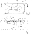
- a circuit board 100 serving as a separator between a vacuum region and a pressure region of a vacuum device such as that described above in connection with US Pat Fig. 1 described vacuum pump 10 can be used.
- the circuit board 100 comprises three contact points facing the viewer 102, which are each connected via a inside lying in the board 100 and therefore indicated by dashed lines conductor 104 with a formed as a via contact point 106.
- a support 108 for a sealing element extends around the contact points 102 in a ring shape.
- The, in particular flat, shape of the support 108 and / or the sealing element describes, for example, a closed ring, preferably a circular ring.
- the shape can also have, for example, an arbitrarily complex shape or geometry. For example, a square rounded at the corners, or generally any polygon with or without arc segments, may be named as basic shapes instead of corners.
- complex sealing elements for example a molded seal with more than one sealing area (for details see EP3135917A1 )
- the bearing surface may accordingly consist of several different, composite geometric elements.
- the circuit board 100 also includes a plurality of formed as bores 110 mounting recesses.
- the fastening recesses are arranged around the support surface in such a way that they are at least predominantly uniformly spaced from one another and from the support surface, eg in order to enable the best possible evenly distributed pressing of the support with the sealing element during attachment of the circuit board.
- Fig. 3 is the 100 board Fig. 2 shown in a sectional view, wherein the cutting plane in Fig. 2 is indicated by AA.
- Fig. 3 is also indicated by dashed lines, as the circuit board 100 is attached to a housing 112 of a vacuum device. This is done by means of screws 114, which clamp the circuit board 100 against the housing 112, wherein between the support 108 and the housing 112 as an O-ring 116 formed sealing element is compressed.
- a pressure element between the screws 114 and the circuit board 100 may be arranged, the uniformity of the pressing of the circuit board 100 and thus the support 108 and the O-ring 116 to the housing 112 over the circumference of the support improved.
- the pressure element or the board has projections in the region of the support, for example by additional strip conductors on or between the carrier layers, or outside the region recesses which concentrate the contact forces of the screws 114 predominantly on the area of the support 108.
- the circuit board 100 is embodied in an electrically three-layered manner and comprises two carrier layers 118 and 120.
- the conductor 104 which connects the contact points 102 and 106 with one another, extends between the carrier layers 118 and 120, ie it is formed on the inside.
- a connection conductor 122 or 124 for example, for connecting a drive on the one hand and a controller on the other hand is provided.
- a vacuum region 126 is defined, in which the contact point 102 of the circuit board 100 is located.
- the connection conductor 122 is thus laid in the vacuum region 126 and serves to connect an electrical component located in the vacuum region, for example a drive motor for a vacuum pump.
- the contact point 106 is arranged in a pressure region 128, both with its housing 112 facing side and with its side facing away from the housing 112.
- the vacuum region 126 is separated from the pressure region 128 by the carrier layers 118 and 120 and by the O-ring 116 in conjunction with the overlay 108.
- a support 200 is shown for a sealing element, which is arranged on an outer side of the board, not shown here.
- the structure of the support 108 of the board 100 of FIGS. 2 and 3 may for example correspond to the structure of the support 200 described in more detail below.
- the support 200 comprises a first copper layer 202, which is applied directly to a support layer of the circuit board, which is likewise not shown here and formed in its shape by etching.
- a second copper layer 204 is, for example, electrolytically or galvanically applied to the first copper layer 202.
- a nickel layer 206 is deposited on the second copper layer 204, however, prior to the deposition of the nickel layer 206, a contact surface 208 of the second copper layer 204 has been planarized to enhance the mechanical connection between the second copper layer 204 and the nickel layer 206.
- a bearing surface 210 for a sealing element is formed by a thin gold layer 212, which is applied to the nickel layer 206.
- a circuit board 300 having five layers of carrier layers 302, 304, 306, 308, and 310 is shown.
- the circuit board 300 separates a vacuum region 312 defined in an indicated housing 314 from a pressure region 316.
- In the vacuum region 312 are two contact points 318 and 320 of the circuit board 300 which are connected to contact points of the circuit board 300 in the pressure region 316.
- the contact point 320 is connected to the contact point 322 via a plurality of plated-through holes and internal conductors and thus enables electrical contacting between the vacuum region 312 and the pressure region 316.
- the circuit board 300 has a support 324, via which the circuit board 300 compresses an O-ring 326 against the housing 314.
- a contact surface which has a length L10 transverse to the O-ring 326, which is also referred to as a sealing length, as it describes the length of a fluid path in the seal .
- the sealing length L10 forms a direct connection between the vacuum region 312 and the pressure region 316.
- it can be, for example, with a support according to Fig. 4 , seal very well.
- a dummy conductor 332 that is to say a non-wired conductor.
- the blind conductor 332 extends at least partially around the conductor 330, which, however, in the selected sectional view of Fig. 5 is not visible.
- further dummy conductors 334, 336 and 338 are provided.
- An optimally designed board is characterized by the smallest possible size and thus conductor lengths with the best possible tightness. For this purpose, it proves to be advantageous to tune the individual leaks of the fluid paths so that no path disadvantageously overly leaking, so for example too short or unfavorably excessively dense, so for example, too long, running.
- An exemplary network may be based on the board 100 in FIG Fig. 2 and Fig. 3 be set up.
- the first group of three mutually parallel fluid paths begins at the three contact points 106 with adjacent ambient pressure in the pressure range 128. From there, the three paths each extend in series through the via through the support layer 118 along the three conductors 104 each with specific tightness over its length to the vias through the carrier layer 120 and terminate at the contact points 102 to vacuum pressure in the vacuum region 126th
- a second group of fluid paths is located in the area of the support 108, here there are several parallel paths between and through the material layers the carrier layer 120, the support 108, the O-ring 116 and the housing 112, which each begin at its two opposite sides in the pressure region 128 and end in the vacuum region 126.
- the fluid paths are not long in the region of the O-ring 116, but very wide.
- the length of the fluid path between support 108 and O-ring 116 is, for example, according to Fig. 5 defined with the sealing length L10, the width or sealing width can be approximately described with the central circumference of the support 108.
- a partial path can be formed based on the specific impermeability of the material of the carrier layers 118 and 120 with an intermediate bond, in which case the wall thicknesses of the carrier layers and the entire enclosed surface in the support ring 108 are variables.
- a further partial path is formed along the through-connection between contact point 102 and conductor 104 with the thickness of the carrier layer 120 as a length; this path continues through the wall thickness of the carrier layer 118 according to previous embodiments. Another path continues between the carrier layers in the region of the bond on the shortest possible path to the edges of the carrier layers.
- the three mentioned groups of fluid paths can be viewed in the overall network as being paralleled or functionally parallel, but on closer inspection these influence each other at least partially, for example the first-mentioned fluid paths predominantly in the area of the via at contact point 102 with the latter .
- a total tightness of the area "housing with board” can be determined and checked against the need.
- the network calculation can be used to identify fluid paths that are excessively leaky or close to other paths. By constructive adaptation, these areas can be made denser or more compact or simpler, so that after an optimization according to the network calculation, all the fluid paths of the board are at least similarly dense in order to achieve an efficient overall solution.
- the middle of the three conductors 104 will be shorter because, as shown, this would result in an unnecessarily higher average density over its two adjacent conductors due to its relatively greater length along the fluid path.
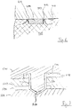
- Fig. 6 For example, two carrier layers 400 and 402 of a board, shown only partially here, are shown in a sectional view embedding an inner conductor 404.
- the conductor 404 was formed by etching from a raw board constituting the carrier layer 400.
- the carrier layer 402 was applied to the carrier layer 400 after forming the conductor 404 or after the etching.
- the backing layer 402 comprises a relatively viscous material upon application, such as an epoxy resin, which conforms to the conductor 404 and the backing layer 400, but leaving imperfections 406, 408, and 410, respectively.
- a smooth surface of the conductor 404 facing the carrier layer 402 is usually relatively evenly connected when the carrier layer 402 is applied.
- the resistance to a fluid to be sealed is low, especially in one direction along the conductor through the defects 406 and 408, ie perpendicular to the image plane.
- the fluid path along the conductor 404 can thus be difficult to seal.
- the conductor 404 or the corresponding fluid path can therefore be particularly long and / or complex, so as to increase the total resistance of the fluid path or its tightness.
- Fig. 7 For example, three carrier layers 500, 502 and 504 of a circuit board are shown, wherein a through-connection 506 for connecting two conductors 508 and 510 is provided between two contact surfaces of respectively two adjacent carrier layers 500, 502, 504.
- the board of the Fig. 7 is prepared by first completely coating the carrier layer 504 with copper. Such a coated carrier layer can also be provided as a raw board. Subsequently, the conductor 510 is etched from the copper coating of the carrier layer 504. Subsequently, the carrier layer 502 is applied to the carrier layer 504 and the conductor 510. To form the conductor 508, the carrier layer 502 is also completely coated with copper and the conductor 508 is etched. Then, the via 506 is made by forming a bore 512 in FIG Fig. 7 from above through the conductor 508 and the conductor 510 is introduced.
- an additional copper layer 514 is deposited electrolytically or galvanically in the bore 512 and at contact surfaces to the conductors 508 and 510.
- the carrier layer 500 is applied to the carrier layer 502 and the conductor 508 at elevated temperature and / or elevated pressure or introduced into the plated-through hole 506 so that a carrier material of the carrier layer 500 fills the through-connection 506 as completely as possible.
- defects 516 in particular at the bottom of the bore 512 or the plated-through hole 506, can also remain here.
- the hole 512 completely penetrates both conductors 508 and 510. According to an alternative embodiment, which is not shown separately, it may be provided that the bore 512 does not or not completely penetrate the conductor 510. Thus, the tightness in the region of the via 506 can be further increased.
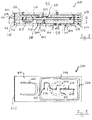
- FIG. 8 For example, another circuit board 600 having five carrier layers 602, 604, 606, 608, and 610 is shown.
- the circuit board 600 separates a vacuum region 612 from a pressure region 614 and compresses an O-ring 616 over a support 618.
- the circuit board 600 has a plurality of cavities 620, 622, 624 and 626, which are formed in this embodiment as cavities, but also, for example, to further improve the sealing effect of the board 600, may be filled.
- cavities 620, 622, 624 and 626 which are formed in this embodiment as cavities, but also, for example, to further improve the sealing effect of the board 600, may be filled.
- electrical components 628 and 630 are arranged in the cavities.
- Fig. 9 the circuit board 600 is shown in a section along a sectional plane BB.
- the sectional plane BB runs along an interface between the carrier layers 608 and 610. Since the view of the Fig. 9 a view in Fig. 8 from above, only the carrier layer 610 is visible.
- a stub conductor 644 Extending around the conductors 632 and 634 is a stub conductor 644 which completely encloses the conductors 632 and 634 in their plane to seal the region of the conductors 632 and 634.
- a further dummy conductor 646 is provided which partially surrounds the cavity 620.
- the board 600 has an edge seal 648, which in the 8 and 9 left area of the board 600 further seals.
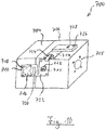
- a vacuum device 700 according to the invention is shown with a circuit board 702, which is designed as a multi-acting separating element for separating a vacuum region from a pressure region.
- the vacuum apparatus 700 includes a two-part housing 704, 706 having a vacuum flange 708 for connection to a vacuum recipient, not shown or a process structure.
- the two housing parts 704, 706 are sealed to each other with a circumferential seal, not shown. Both housing parts have electrical cable feedthroughs between the inner vacuum and the surrounding pressure range, which is realized with the multi-sections 710, 712, 714 comprising board 702.
- a first portion 710 with a dashed line indicated, between board and housing lying seal is located on the front of the first housing part 704.
- a support of the first portion 710 for a sealing element is by a pressure element 716 with four screws 718 through the board 702 therethrough evenly pressed.
- Electrical connections are guided by the board 702 from the inner vacuum area in printed conductors, not shown, which lead via a meandering, flexibly deformable connecting portion 720 on the second portion 712, which is arranged on the front of the second housing part 706, to the electrical connection 722.
- connection region makes it possible to compensate differences in height and planarity between the two housing parts 704, 706 joined to one another with tolerance, so that both partial regions 710, 712 of the printed circuit board 702 can rest against the housing parts 704 or 706 to the greatest possible extent independently of one another.
- the third subarea 714 of the board 702 is arranged on the upper side of the second housing part 706 and electrically connected to the second subarea 712 of the board 702 by means of a flexible flat cable 724.
- An unillustrated sealing area between the third portion 714 and the second housing portion 706 under a pressure element 726, which is biased by a lying outside the board 702 screw 728 leads more electrical connections from the vacuum area on the board 702 and via the flexible conductors of the flat cable 724 to the electrical connection 722 on the second portion 712 of the board 702nd
- the pressure element 726 acts as a distributing and balancing element.
Landscapes
- Engineering & Computer Science (AREA)
- Mechanical Engineering (AREA)
- General Engineering & Computer Science (AREA)
- Microelectronics & Electronic Packaging (AREA)
- Manufacturing & Machinery (AREA)
- Structures Of Non-Positive Displacement Pumps (AREA)
- Non-Positive Displacement Air Blowers (AREA)
- Gasket Seals (AREA)
- Mounting Of Printed Circuit Boards And The Like (AREA)
- Printing Elements For Providing Electric Connections Between Printed Circuits (AREA)
Priority Applications (2)
| Application Number | Priority Date | Filing Date | Title |
|---|---|---|---|
| EP17195789.7A EP3470681B1 (fr) | 2017-10-10 | 2017-10-10 | Traverse électrique pour appareil à vide, sous la forme d'une plaque de circuit imprimé |
| JP2018189659A JP6861191B2 (ja) | 2017-10-10 | 2018-10-05 | 真空装置 |
Applications Claiming Priority (1)
| Application Number | Priority Date | Filing Date | Title |
|---|---|---|---|
| EP17195789.7A EP3470681B1 (fr) | 2017-10-10 | 2017-10-10 | Traverse électrique pour appareil à vide, sous la forme d'une plaque de circuit imprimé |
Publications (2)
| Publication Number | Publication Date |
|---|---|
| EP3470681A1 true EP3470681A1 (fr) | 2019-04-17 |
| EP3470681B1 EP3470681B1 (fr) | 2021-09-22 |
Family
ID=60083117
Family Applications (1)
| Application Number | Title | Priority Date | Filing Date |
|---|---|---|---|
| EP17195789.7A Active EP3470681B1 (fr) | 2017-10-10 | 2017-10-10 | Traverse électrique pour appareil à vide, sous la forme d'une plaque de circuit imprimé |
Country Status (2)
| Country | Link |
|---|---|
| EP (1) | EP3470681B1 (fr) |
| JP (1) | JP6861191B2 (fr) |
Families Citing this family (1)
| Publication number | Priority date | Publication date | Assignee | Title |
|---|---|---|---|---|
| GB2591500B (en) * | 2020-01-30 | 2022-11-30 | Edwards Ltd | A pump and a set of seals sealing the stator components of such a pump |
Citations (7)
| Publication number | Priority date | Publication date | Assignee | Title |
|---|---|---|---|---|
| JP2003254849A (ja) * | 2002-02-28 | 2003-09-10 | Sunx Ltd | 圧力検出器及び圧力センサ |
| JP2005069209A (ja) * | 2003-08-28 | 2005-03-17 | Fuji Electric Holdings Co Ltd | コールドトラップおよび真空排気装置 |
| EP1843043A2 (fr) * | 2006-04-07 | 2007-10-10 | Pfeiffer Vacuum Gmbh | Pompe à vide avec un appareil d'entraînement |
| JP2014011120A (ja) * | 2012-07-02 | 2014-01-20 | Shimadzu Corp | 電気フィードスルー、真空ポンプおよびプリント基板 |
| WO2014068848A1 (fr) * | 2012-10-31 | 2014-05-08 | タイコエレクトロニクスジャパン合同会社 | Connecteur |
| US20140322936A1 (en) * | 2013-04-24 | 2014-10-30 | Tyco Electronics Japan G.K. | Electrical Connector Assembly and Mounting Structure Thereof |
| EP3135917A1 (fr) | 2015-08-24 | 2017-03-01 | Pfeiffer Vacuum Gmbh | Pompe à vide |
Family Cites Families (2)
| Publication number | Priority date | Publication date | Assignee | Title |
|---|---|---|---|---|
| JP2004356188A (ja) * | 2003-05-27 | 2004-12-16 | Sony Corp | 素子内蔵用空所の形成方法及び素子内蔵基板 |
| US20110024898A1 (en) * | 2009-07-31 | 2011-02-03 | Ati Technologies Ulc | Method of manufacturing substrates having asymmetric buildup layers |
-
2017
- 2017-10-10 EP EP17195789.7A patent/EP3470681B1/fr active Active
-
2018
- 2018-10-05 JP JP2018189659A patent/JP6861191B2/ja active Active
Patent Citations (7)
| Publication number | Priority date | Publication date | Assignee | Title |
|---|---|---|---|---|
| JP2003254849A (ja) * | 2002-02-28 | 2003-09-10 | Sunx Ltd | 圧力検出器及び圧力センサ |
| JP2005069209A (ja) * | 2003-08-28 | 2005-03-17 | Fuji Electric Holdings Co Ltd | コールドトラップおよび真空排気装置 |
| EP1843043A2 (fr) * | 2006-04-07 | 2007-10-10 | Pfeiffer Vacuum Gmbh | Pompe à vide avec un appareil d'entraînement |
| JP2014011120A (ja) * | 2012-07-02 | 2014-01-20 | Shimadzu Corp | 電気フィードスルー、真空ポンプおよびプリント基板 |
| WO2014068848A1 (fr) * | 2012-10-31 | 2014-05-08 | タイコエレクトロニクスジャパン合同会社 | Connecteur |
| US20140322936A1 (en) * | 2013-04-24 | 2014-10-30 | Tyco Electronics Japan G.K. | Electrical Connector Assembly and Mounting Structure Thereof |
| EP3135917A1 (fr) | 2015-08-24 | 2017-03-01 | Pfeiffer Vacuum Gmbh | Pompe à vide |
Also Published As
| Publication number | Publication date |
|---|---|
| EP3470681B1 (fr) | 2021-09-22 |
| JP2019070386A (ja) | 2019-05-09 |
| JP6861191B2 (ja) | 2021-04-21 |
Similar Documents
| Publication | Publication Date | Title |
|---|---|---|
| EP3289669B1 (fr) | Machine électrique sans boîtier | |
| DE2353615C2 (de) | Verfahren zum Herstellen eines elektrischen Verbinders | |
| DE102016217872A1 (de) | Lagerdichtung mit integrierter Erdungsbürste | |
| DE10137785A1 (de) | Elektrokorrosionsbeständiger Wälzlageraufbau | |
| DE102018129229A1 (de) | Elektrische Maschine mit mehreren als Hohlleiter ausgebildeten starren Wicklungsstücken - hydraulisches Anschlusskonzept I | |
| AT521301A1 (de) | Stator mit Isolationsschicht | |
| DE102019219764A1 (de) | Abtasteinheit zur Abtastung einer Winkelskala sowie Winkelmesseinrichtung mit dieser Abtasteinheit | |
| DE112017001225T5 (de) | Motor und Herstellungsverfahren für einen Motor | |
| EP3470681B1 (fr) | Traverse électrique pour appareil à vide, sous la forme d'une plaque de circuit imprimé | |
| EP3973599B1 (fr) | Émetteur rotatif pour signaux haute fréquence | |
| DE102019209212A1 (de) | Motor | |
| DE102006022772A1 (de) | Antriebsanordnung für eine Vakuumpumpe | |
| WO2022111747A1 (fr) | Roulement | |
| EP3431769B1 (fr) | Pompe à vide | |
| WO2006029984A1 (fr) | Machine électrique | |
| DE10237324A1 (de) | Verfahren zur Herstellung einer Elektrode für die elektrochemische Bearbeitung eines Werkstücks und nach dem Verfahren hergestellte Elektrode | |
| DE102007041898A1 (de) | Kraftstoffpumpe | |
| EP3061178A2 (fr) | Joint en labyrinthe pour machines triphasées | |
| DE102010014970B4 (de) | Elektrode und Verfahren zur elektrochemischen Bearbeitung eines metallischen Lagerbauteils | |
| EP3536966B1 (fr) | Appareil à vide | |
| WO2022112009A2 (fr) | Élément stator d'une machine électrodynamique | |
| DE102018216017A1 (de) | Verfahren zur Herstellung eines Stators, Stator und Elektromaschine | |
| DE102019113898A1 (de) | Lager | |
| AT518722B1 (de) | Elektrode zur elektrochemischen Bearbeitung eines metallischen Werkstücks | |
| EP2390990A1 (fr) | Moteur linéaire |
Legal Events
| Date | Code | Title | Description |
|---|---|---|---|
| PUAI | Public reference made under article 153(3) epc to a published international application that has entered the european phase |
Free format text: ORIGINAL CODE: 0009012 |
|
| STAA | Information on the status of an ep patent application or granted ep patent |
Free format text: STATUS: THE APPLICATION HAS BEEN PUBLISHED |
|
| AK | Designated contracting states |
Kind code of ref document: A1 Designated state(s): AL AT BE BG CH CY CZ DE DK EE ES FI FR GB GR HR HU IE IS IT LI LT LU LV MC MK MT NL NO PL PT RO RS SE SI SK SM TR |
|
| AX | Request for extension of the european patent |
Extension state: BA ME |
|
| STAA | Information on the status of an ep patent application or granted ep patent |
Free format text: STATUS: REQUEST FOR EXAMINATION WAS MADE |
|
| 17P | Request for examination filed |
Effective date: 20190701 |
|
| RBV | Designated contracting states (corrected) |
Designated state(s): AL AT BE BG CH CY CZ DE DK EE ES FI FR GB GR HR HU IE IS IT LI LT LU LV MC MK MT NL NO PL PT RO RS SE SI SK SM TR |
|
| GRAP | Despatch of communication of intention to grant a patent |
Free format text: ORIGINAL CODE: EPIDOSNIGR1 |
|
| STAA | Information on the status of an ep patent application or granted ep patent |
Free format text: STATUS: GRANT OF PATENT IS INTENDED |
|
| INTG | Intention to grant announced |
Effective date: 20210430 |
|
| GRAS | Grant fee paid |
Free format text: ORIGINAL CODE: EPIDOSNIGR3 |
|
| GRAA | (expected) grant |
Free format text: ORIGINAL CODE: 0009210 |
|
| STAA | Information on the status of an ep patent application or granted ep patent |
Free format text: STATUS: THE PATENT HAS BEEN GRANTED |
|
| AK | Designated contracting states |
Kind code of ref document: B1 Designated state(s): AL AT BE BG CH CY CZ DE DK EE ES FI FR GB GR HR HU IE IS IT LI LT LU LV MC MK MT NL NO PL PT RO RS SE SI SK SM TR |
|
| REG | Reference to a national code |
Ref country code: GB Ref legal event code: FG4D Free format text: NOT ENGLISH |
|
| REG | Reference to a national code |
Ref country code: DE Ref legal event code: R096 Ref document number: 502017011550 Country of ref document: DE |
|
| REG | Reference to a national code |
Ref country code: IE Ref legal event code: FG4D Free format text: LANGUAGE OF EP DOCUMENT: GERMAN |
|
| REG | Reference to a national code |
Ref country code: CH Ref legal event code: EP Ref country code: AT Ref legal event code: REF Ref document number: 1432540 Country of ref document: AT Kind code of ref document: T Effective date: 20211015 |
|
| REG | Reference to a national code |
Ref country code: LT Ref legal event code: MG9D |
|
| REG | Reference to a national code |
Ref country code: NL Ref legal event code: MP Effective date: 20210922 |
|
| PG25 | Lapsed in a contracting state [announced via postgrant information from national office to epo] |
Ref country code: SE Free format text: LAPSE BECAUSE OF FAILURE TO SUBMIT A TRANSLATION OF THE DESCRIPTION OR TO PAY THE FEE WITHIN THE PRESCRIBED TIME-LIMIT Effective date: 20210922 Ref country code: RS Free format text: LAPSE BECAUSE OF FAILURE TO SUBMIT A TRANSLATION OF THE DESCRIPTION OR TO PAY THE FEE WITHIN THE PRESCRIBED TIME-LIMIT Effective date: 20210922 Ref country code: HR Free format text: LAPSE BECAUSE OF FAILURE TO SUBMIT A TRANSLATION OF THE DESCRIPTION OR TO PAY THE FEE WITHIN THE PRESCRIBED TIME-LIMIT Effective date: 20210922 Ref country code: LT Free format text: LAPSE BECAUSE OF FAILURE TO SUBMIT A TRANSLATION OF THE DESCRIPTION OR TO PAY THE FEE WITHIN THE PRESCRIBED TIME-LIMIT Effective date: 20210922 Ref country code: BG Free format text: LAPSE BECAUSE OF FAILURE TO SUBMIT A TRANSLATION OF THE DESCRIPTION OR TO PAY THE FEE WITHIN THE PRESCRIBED TIME-LIMIT Effective date: 20211222 Ref country code: NO Free format text: LAPSE BECAUSE OF FAILURE TO SUBMIT A TRANSLATION OF THE DESCRIPTION OR TO PAY THE FEE WITHIN THE PRESCRIBED TIME-LIMIT Effective date: 20211222 Ref country code: FI Free format text: LAPSE BECAUSE OF FAILURE TO SUBMIT A TRANSLATION OF THE DESCRIPTION OR TO PAY THE FEE WITHIN THE PRESCRIBED TIME-LIMIT Effective date: 20210922 |
|
| PG25 | Lapsed in a contracting state [announced via postgrant information from national office to epo] |
Ref country code: LV Free format text: LAPSE BECAUSE OF FAILURE TO SUBMIT A TRANSLATION OF THE DESCRIPTION OR TO PAY THE FEE WITHIN THE PRESCRIBED TIME-LIMIT Effective date: 20210922 Ref country code: GR Free format text: LAPSE BECAUSE OF FAILURE TO SUBMIT A TRANSLATION OF THE DESCRIPTION OR TO PAY THE FEE WITHIN THE PRESCRIBED TIME-LIMIT Effective date: 20211223 |
|
| REG | Reference to a national code |
Ref country code: CH Ref legal event code: PL |
|
| PG25 | Lapsed in a contracting state [announced via postgrant information from national office to epo] |
Ref country code: IS Free format text: LAPSE BECAUSE OF FAILURE TO SUBMIT A TRANSLATION OF THE DESCRIPTION OR TO PAY THE FEE WITHIN THE PRESCRIBED TIME-LIMIT Effective date: 20220122 Ref country code: SK Free format text: LAPSE BECAUSE OF FAILURE TO SUBMIT A TRANSLATION OF THE DESCRIPTION OR TO PAY THE FEE WITHIN THE PRESCRIBED TIME-LIMIT Effective date: 20210922 Ref country code: RO Free format text: LAPSE BECAUSE OF FAILURE TO SUBMIT A TRANSLATION OF THE DESCRIPTION OR TO PAY THE FEE WITHIN THE PRESCRIBED TIME-LIMIT Effective date: 20210922 Ref country code: PT Free format text: LAPSE BECAUSE OF FAILURE TO SUBMIT A TRANSLATION OF THE DESCRIPTION OR TO PAY THE FEE WITHIN THE PRESCRIBED TIME-LIMIT Effective date: 20220124 Ref country code: PL Free format text: LAPSE BECAUSE OF FAILURE TO SUBMIT A TRANSLATION OF THE DESCRIPTION OR TO PAY THE FEE WITHIN THE PRESCRIBED TIME-LIMIT Effective date: 20210922 Ref country code: NL Free format text: LAPSE BECAUSE OF FAILURE TO SUBMIT A TRANSLATION OF THE DESCRIPTION OR TO PAY THE FEE WITHIN THE PRESCRIBED TIME-LIMIT Effective date: 20210922 Ref country code: ES Free format text: LAPSE BECAUSE OF FAILURE TO SUBMIT A TRANSLATION OF THE DESCRIPTION OR TO PAY THE FEE WITHIN THE PRESCRIBED TIME-LIMIT Effective date: 20210922 Ref country code: EE Free format text: LAPSE BECAUSE OF FAILURE TO SUBMIT A TRANSLATION OF THE DESCRIPTION OR TO PAY THE FEE WITHIN THE PRESCRIBED TIME-LIMIT Effective date: 20210922 Ref country code: AL Free format text: LAPSE BECAUSE OF FAILURE TO SUBMIT A TRANSLATION OF THE DESCRIPTION OR TO PAY THE FEE WITHIN THE PRESCRIBED TIME-LIMIT Effective date: 20210922 |
|
| REG | Reference to a national code |
Ref country code: DE Ref legal event code: R097 Ref document number: 502017011550 Country of ref document: DE Ref country code: BE Ref legal event code: MM Effective date: 20211031 |
|
| PG25 | Lapsed in a contracting state [announced via postgrant information from national office to epo] |
Ref country code: MC Free format text: LAPSE BECAUSE OF FAILURE TO SUBMIT A TRANSLATION OF THE DESCRIPTION OR TO PAY THE FEE WITHIN THE PRESCRIBED TIME-LIMIT Effective date: 20210922 |
|
| PG25 | Lapsed in a contracting state [announced via postgrant information from national office to epo] |
Ref country code: LU Free format text: LAPSE BECAUSE OF NON-PAYMENT OF DUE FEES Effective date: 20211010 Ref country code: DK Free format text: LAPSE BECAUSE OF FAILURE TO SUBMIT A TRANSLATION OF THE DESCRIPTION OR TO PAY THE FEE WITHIN THE PRESCRIBED TIME-LIMIT Effective date: 20210922 Ref country code: BE Free format text: LAPSE BECAUSE OF NON-PAYMENT OF DUE FEES Effective date: 20211031 |
|
| PLBE | No opposition filed within time limit |
Free format text: ORIGINAL CODE: 0009261 |
|
| STAA | Information on the status of an ep patent application or granted ep patent |
Free format text: STATUS: NO OPPOSITION FILED WITHIN TIME LIMIT |
|
| 26N | No opposition filed |
Effective date: 20220623 |
|
| PG25 | Lapsed in a contracting state [announced via postgrant information from national office to epo] |
Ref country code: LI Free format text: LAPSE BECAUSE OF NON-PAYMENT OF DUE FEES Effective date: 20211031 Ref country code: CH Free format text: LAPSE BECAUSE OF NON-PAYMENT OF DUE FEES Effective date: 20211031 |
|
| PG25 | Lapsed in a contracting state [announced via postgrant information from national office to epo] |
Ref country code: IE Free format text: LAPSE BECAUSE OF NON-PAYMENT OF DUE FEES Effective date: 20211010 |
|
| PG25 | Lapsed in a contracting state [announced via postgrant information from national office to epo] |
Ref country code: SI Free format text: LAPSE BECAUSE OF FAILURE TO SUBMIT A TRANSLATION OF THE DESCRIPTION OR TO PAY THE FEE WITHIN THE PRESCRIBED TIME-LIMIT Effective date: 20210922 Ref country code: FR Free format text: LAPSE BECAUSE OF NON-PAYMENT OF DUE FEES Effective date: 20211122 |
|
| PG25 | Lapsed in a contracting state [announced via postgrant information from national office to epo] |
Ref country code: CY Free format text: LAPSE BECAUSE OF FAILURE TO SUBMIT A TRANSLATION OF THE DESCRIPTION OR TO PAY THE FEE WITHIN THE PRESCRIBED TIME-LIMIT Effective date: 20210922 |
|
| PG25 | Lapsed in a contracting state [announced via postgrant information from national office to epo] |
Ref country code: SM Free format text: LAPSE BECAUSE OF FAILURE TO SUBMIT A TRANSLATION OF THE DESCRIPTION OR TO PAY THE FEE WITHIN THE PRESCRIBED TIME-LIMIT Effective date: 20210922 Ref country code: HU Free format text: LAPSE BECAUSE OF FAILURE TO SUBMIT A TRANSLATION OF THE DESCRIPTION OR TO PAY THE FEE WITHIN THE PRESCRIBED TIME-LIMIT; INVALID AB INITIO Effective date: 20171010 |
|
| REG | Reference to a national code |
Ref country code: AT Ref legal event code: MM01 Ref document number: 1432540 Country of ref document: AT Kind code of ref document: T Effective date: 20221010 |
|
| PG25 | Lapsed in a contracting state [announced via postgrant information from national office to epo] |
Ref country code: AT Free format text: LAPSE BECAUSE OF NON-PAYMENT OF DUE FEES Effective date: 20221010 |
|
| PG25 | Lapsed in a contracting state [announced via postgrant information from national office to epo] |
Ref country code: MK Free format text: LAPSE BECAUSE OF FAILURE TO SUBMIT A TRANSLATION OF THE DESCRIPTION OR TO PAY THE FEE WITHIN THE PRESCRIBED TIME-LIMIT Effective date: 20210922 |
|
| PG25 | Lapsed in a contracting state [announced via postgrant information from national office to epo] |
Ref country code: TR Free format text: LAPSE BECAUSE OF FAILURE TO SUBMIT A TRANSLATION OF THE DESCRIPTION OR TO PAY THE FEE WITHIN THE PRESCRIBED TIME-LIMIT Effective date: 20210922 |
|
| PG25 | Lapsed in a contracting state [announced via postgrant information from national office to epo] |
Ref country code: MT Free format text: LAPSE BECAUSE OF FAILURE TO SUBMIT A TRANSLATION OF THE DESCRIPTION OR TO PAY THE FEE WITHIN THE PRESCRIBED TIME-LIMIT Effective date: 20210922 |
|
| PGFP | Annual fee paid to national office [announced via postgrant information from national office to epo] |
Ref country code: GB Payment date: 20251022 Year of fee payment: 9 |
|
| PGFP | Annual fee paid to national office [announced via postgrant information from national office to epo] |
Ref country code: IT Payment date: 20251024 Year of fee payment: 9 |
|
| PGFP | Annual fee paid to national office [announced via postgrant information from national office to epo] |
Ref country code: CZ Payment date: 20251002 Year of fee payment: 9 |
|
| PGFP | Annual fee paid to national office [announced via postgrant information from national office to epo] |
Ref country code: DE Payment date: 20251229 Year of fee payment: 9 |