EP3477771B1 - Antenne à dipôle imprimé, antenne réseau et dispositif de communications - Google Patents
Antenne à dipôle imprimé, antenne réseau et dispositif de communications Download PDFInfo
- Publication number
- EP3477771B1 EP3477771B1 EP18202719.3A EP18202719A EP3477771B1 EP 3477771 B1 EP3477771 B1 EP 3477771B1 EP 18202719 A EP18202719 A EP 18202719A EP 3477771 B1 EP3477771 B1 EP 3477771B1
- Authority
- EP
- European Patent Office
- Prior art keywords
- feed line
- printed dipole
- segment
- antenna
- printed
- Prior art date
- Legal status (The legal status is an assumption and is not a legal conclusion. Google has not performed a legal analysis and makes no representation as to the accuracy of the status listed.)
- Active
Links
Images




Classifications
-
- H—ELECTRICITY
- H01—ELECTRIC ELEMENTS
- H01Q—ANTENNAS, i.e. RADIO AERIALS
- H01Q21/00—Antenna arrays or systems
- H01Q21/06—Arrays of individually energised antenna units similarly polarised and spaced apart
- H01Q21/061—Two dimensional planar arrays
- H01Q21/062—Two dimensional planar arrays using dipole aerials
-
- H—ELECTRICITY
- H01—ELECTRIC ELEMENTS
- H01Q—ANTENNAS, i.e. RADIO AERIALS
- H01Q1/00—Details of, or arrangements associated with, antennas
- H01Q1/36—Structural form of radiating elements, e.g. cone, spiral, umbrella; Particular materials used therewith
- H01Q1/38—Structural form of radiating elements, e.g. cone, spiral, umbrella; Particular materials used therewith formed by a conductive layer on an insulating support
-
- H—ELECTRICITY
- H01—ELECTRIC ELEMENTS
- H01Q—ANTENNAS, i.e. RADIO AERIALS
- H01Q21/00—Antenna arrays or systems
- H01Q21/0006—Particular feeding systems
-
- H—ELECTRICITY
- H01—ELECTRIC ELEMENTS
- H01Q—ANTENNAS, i.e. RADIO AERIALS
- H01Q21/00—Antenna arrays or systems
- H01Q21/0006—Particular feeding systems
- H01Q21/0025—Modular arrays
-
- H—ELECTRICITY
- H01—ELECTRIC ELEMENTS
- H01Q—ANTENNAS, i.e. RADIO AERIALS
- H01Q21/00—Antenna arrays or systems
- H01Q21/0087—Apparatus or processes specially adapted for manufacturing antenna arrays
-
- H—ELECTRICITY
- H01—ELECTRIC ELEMENTS
- H01Q—ANTENNAS, i.e. RADIO AERIALS
- H01Q21/00—Antenna arrays or systems
- H01Q21/06—Arrays of individually energised antenna units similarly polarised and spaced apart
- H01Q21/08—Arrays of individually energised antenna units similarly polarised and spaced apart the units being spaced along or adjacent to a rectilinear path
- H01Q21/12—Parallel arrangements of substantially straight elongated conductive units
-
- H—ELECTRICITY
- H01—ELECTRIC ELEMENTS
- H01Q—ANTENNAS, i.e. RADIO AERIALS
- H01Q5/00—Arrangements for simultaneous operation of antennas on two or more different wavebands, e.g. dual-band or multi-band arrangements
- H01Q5/30—Arrangements for providing operation on different wavebands
- H01Q5/307—Individual or coupled radiating elements, each element being fed in an unspecified way
- H01Q5/342—Individual or coupled radiating elements, each element being fed in an unspecified way for different propagation modes
- H01Q5/35—Individual or coupled radiating elements, each element being fed in an unspecified way for different propagation modes using two or more simultaneously fed points
-
- H—ELECTRICITY
- H01—ELECTRIC ELEMENTS
- H01Q—ANTENNAS, i.e. RADIO AERIALS
- H01Q9/00—Electrically-short antennas having dimensions not more than twice the operating wavelength and consisting of conductive active radiating elements
- H01Q9/04—Resonant antennas
- H01Q9/06—Details
- H01Q9/065—Microstrip dipole antennas
Definitions
- This disclosure relates to the field of wireless communications technologies, and in particular, to a printed dipole antenna, an array antenna, and a communications device.
- a wireless local area network is widely applied to a home, an office, and another indoor/outdoor environment.
- WLAN wireless local area network
- a high-density deployment scenario for example, a stadium, where a height of an antenna above a ground is approximately 15 m to 50 m
- a small-angle directional antenna needs to be used to reduce a coverage radius of a single access point device.
- a sidelobe suppression capability of the directional antenna determines a capability to suppress co-channel interference between adjacent access point devices in the high-density deployment scenario.
- US 6,831,602 relates to low cost trombone line beamformer.
- US 6,285,323 relates to flat plate antenna arrays.
- US 8,200,168 relates to programmable antenna assembly and applications thereof.
- This disclosure is intended to reduce co-channel interference between adjacent access point devices in a high-density deployment scenario.
- the feed lines parallel to the printed dipoles each include different segments, and each segment approaches a printed dipole on one side of the segment, to suppress parasitic emission of the feed lines, and implement a low sidelobe level of the printed dipole antenna.
- the low sidelobe level of the printed dipole antenna is implemented within a 5GHz frequency band by setting the lengths of the first segment, the second segment, the third segment, and the fourth segment of the feed lines and the related distances.
- printed dipoles of adjacent printed dipole antennas of the array antenna are perpendicular to each other, reducing parasitic emission between the adjacent printed dipole antennas, and implementing a low sidelobe level of the array antenna.
- the feed lines parallel to the printed dipoles of the printed dipole antennas each include different segments, and each segment approaches a printed dipole antenna on one side of the segment, to suppress parasitic emission of the feed lines between the printed dipole antennas, and implement a low sidelobe level of the array antenna.
- printed dipoles of adjacent printed dipole antennas of the array antenna are perpendicular to each other, reducing parasitic emission between the adjacent printed dipole antennas, and implementing a low sidelobe level of the array antenna.
- FIG. 1 shows a printed dipole antenna according to an aspect of the present disclosure.
- the printed dipole antenna includes a first printed dipole 101, a second printed dipole 102, a third printed dipole 103, a fourth printed dipole 104, a first feed line 201, a second feed line 202, a third feed line 203, and a fourth feed line 204.
- Two arms of any one of the first printed dipole 101, the second printed dipole 102, the third printed dipole 103, and the fourth printed dipole 104 are disposed on an upper surface and a lower surface of a dielectric substrate respectively, and extend towards opposite directions.
- any one of the first feed line 201, the second feed line 202, the third feed line 203, and the fourth feed line 204 is disposed on the upper surface and the lower surface of the dielectric substrate.
- the first printed dipole 101 is parallel to the second printed dipole 102, and is perpendicular to the first feed line 201.
- the first printed dipole 101 is connected to one end of the first feed line 201, and the second printed dipole 102 is connected to the other end of the first feed line 201.
- the third printed dipole 103 is parallel to the fourth printed dipole 104, and is perpendicular to the second feed line 202.
- the third printed dipole 103 is connected to one end of the second feed line 202, and the fourth printed dipole 104 is connected to the other end of the second feed line 202.
- One end of the third feed line 203 is connected to the first feed line 201, and a connection point between the third feed line 203 and the first feed line 201 is any point on the first feed line 201 different from the two ends of the first feed line 201.
- the other end of the third feed line 203 is connected to one end of the fourth feed line 204, the other end of the fourth feed line 204 is connected to the second feed line 202, and a connection point between the fourth feed line 204 and the second feed line 202 is any point on the second feed line 202 different from the two ends of the second feed line 202.
- the third feed line 203 includes a first segment 2031 and a second segment 2032
- the fourth feed line 204 includes a third segment 2041 and a fourth segment 2042.
- the first segment 2031 is parallel to the first printed dipole 101, and a distance from the first segment 2031 to the first printed dipole 101 is less than a distance from a midpoint of the first feed line 201 to the first printed dipole 101.
- the second segment 2032 is parallel to the second printed dipole 102, and a distance from the second segment 2032 to the second printed dipole 102 is less than a distance from the midpoint of the first feed line 201 to the second printed dipole 102.
- the third segment 2041 is parallel to the third printed dipole 103, and a distance from the third segment 2041 to the third printed dipole 103 is less than a distance from a midpoint of the second feed line 202 to the third printed dipole 103.
- the fourth segment 2042 is parallel to the fourth printed dipole 104, and a distance from the fourth segment 2042 to the fourth printed dipole 104 is less than a distance from the midpoint of the second feed line 202 to the fourth printed dipole 104.
- the feed lines parallel to the printed dipoles each include different segments, and each segment approaches a printed dipole on one side of the segment, to suppress parasitic emission of the feed lines, and implement a low sidelobe level of the printed dipole antenna.
- a distance from the first segment 2031 to the midpoint of the first feed line 201 is 0.2 to 0.6 times a guided wavelength.
- a distance from the second segment 2032 to the midpoint of the first feed line 201 is 0.2 to 0.6 times the guided wavelength.
- a distance from the third segment 2041 to the midpoint of the second feed line 202 is 0.2 to 0.6 times the guided wavelength.
- a distance from the fourth segment 2042 to the midpoint of the second feed line 202 is 0.2 to 0.6 times the guided wavelength.
- a length of the first segment 2031 is 0.1 to 0.3 times the guided wavelength.
- Alength of the second segment 2032 is 0.1 to 0.3 times the guided wavelength.
- a length of the third segment 2041 is 0.1 to 0.3 times the guided wavelength.
- a length of the fourth segment 2042 is 0.1 to 0.3 times the guided wavelength.
- the feed line is a double-sided parallel-strip line, and therefore the feed line is a waveguide.
- the guided wavelength is a wavelength of electromagnetic wave travelling along an axis of guided wave in the waveguide, that is, a guided wavelength of the feed line.
- the low sidelobe level of the printed dipole antenna is implemented within a 5GHz frequency band by setting the lengths of the first segment 2031, the second segment 2032, the third segment 2041, and the fourth segment 2042 of the feed lines and the related distances.
- One end of the first segment 2031 is connected to the first feed line by using two feed lines, and the two feed lines include a feed line parallel to the first feed line 201 and a feed line perpendicular to the first feed line 201.
- the other end of the first segment 2031 is connected to one end of the second segment 2032 by using a feed line parallel to the first feed line 201, and the other end of the second segment 2032 is connected to the fourth feed line 204.
- One end of the third segment 2041 is connected to the second feed line 202 by using two feed lines, and the two feed lines include one feed line parallel to the second feed line 202 and one feed line perpendicular to the second feed line 202.
- the other end of the third segment 2041 is connected to one end of the fourth segment 2042 by using a feed line parallel to the second feed line 202, and the other end of the fourth segment 2042 is connected to the third feed line 203.
- the feed lines parallel to the printed dipoles are optimized. If the optimized feed line design is applied to an array antenna, a plurality of the printed dipole antennas provided in this aspect of the present disclosure may be used to form an array antenna.
- FIG. 2 is a schematic structural diagram of an array antenna according to Aspect 1 of the present disclosure.
- the array antenna includes four printed dipole antennas, and printed dipoles of any two adjacent printed dipole antennas of the four printed dipole antennas are perpendicular to each other.
- Printed dipoles of adjacent printed dipole antennas of the array antenna are perpendicular to each other, reducing parasitic emission between the adjacent printed dipole antennas, and implementing a low sidelobe level of the array antenna.
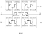
- FIG. 3 is a schematic structural diagram of an array antenna according to Aspect 2 of the present disclosure.
- the array antenna includes a first printed dipole antenna 301, a second printed dipole antenna 302, a third printed dipole antenna 303, a fourth printed dipole antenna 304, a fifth feed line 401, a sixth feed line 402, a seventh feed line 403, and an eighth feed line 404, and all printed dipoles of the four printed dipole antennas are parallel.
- a printed dipole of the first printed dipole antenna 301 is parallel to a printed dipole of the second printed dipole antenna 302, and is perpendicular to the fifth feed line 401.
- the first printed dipole antenna 301 is connected to one end of the fifth feed line 401, and the second printed dipole antenna 302 is connected to the other end of the fifth feed line 401.
- a printed dipole of the third printed dipole antenna 303 is parallel to a printed dipole of the fourth printed dipole antenna 304, and is perpendicular to the sixth feed line 402.
- the third printed dipole antenna 303 is connected to one end of the sixth feed line 402, and the fourth printed dipole antenna 304 is connected to the other end of the sixth feed line 402.
- One end of the seventh feed line 403 is connected to the fifth feed line 401, and a connection point between the seventh feed line 403 and the fifth feed line 401 is any point on the fifth feed line 401 different from the two ends of the fifth feed line 401.
- the other end of the seventh feed line 403 is connected to one end of the eighth feed line 404, the other end of the eighth feed line 404 is connected to the sixth feed line 402, and a connection point between the eighth feed line 404 and the sixth feed line 402 is any point on the sixth feed line 402 different from the two ends of the sixth feed line 402.
- the seventh feed line 403 includes a fifth segment 4031 and a sixth segment 4032
- the eighth feed line 404 includes a seventh segment 4041 and an eighth segment 4042.
- One end of the fifth segment 4031 is connected to the fifth feed line 401 by using two feed lines, and the two feed lines include one feed line parallel to the fifth feed line 401 and one feed line perpendicular to the fifth feed line 401.
- the other end of the fifth segment 4031 is connected to one end of the sixth segment 4032 by using a feed line parallel to the fifth feed line 401, and the other end of the sixth segment 4032 is connected to the eighth feed line 404.
- One end of the seventh segment 4041 is connected to the sixth feed line 402 by using two feed lines, and the two feed lines include one feed line parallel to the sixth feed line 402 and one feed line perpendicular to the sixth feed line 402.
- the other end of the seventh segment 4041 is connected to one end of the eighth segment 4042 by using a feed line parallel to the sixth feed line 402, and the other end of the eighth segment 4042 is connected to the seventh feed line 403.
- the fifth segment 4031 is parallel to the printed dipole of the first printed dipole antenna 301, and a distance from the fifth segment 4031 to the printed dipole of the first printed dipole antenna 301 is less than a distance from a midpoint of the fifth feed line 401 to the printed dipole of the first printed dipole antenna 301.
- the sixth segment 4032 is parallel to the printed dipole of the second printed dipole antenna 302, and a distance from the sixth segment 4032 to the printed dipole of the second printed dipole antenna 302 is less than a distance from the midpoint of the fifth feed line 401 to the printed dipole of the second printed dipole antenna 302.
- the seventh segment 4041 is parallel to the printed dipole of the third printed dipole antenna 303, and a distance from the seventh segment 4041 to the printed dipole of the third printed dipole antenna 303 is less than a distance from a midpoint of the sixth feed line 402 to the printed dipole of the third printed dipole antenna 303.
- the eighth segment 4042 is parallel to the printed dipole of the fourth printed dipole antenna 304, and a distance from the eighth segment 4042 to the printed dipole of the fourth printed dipole antenna 304 is less than a distance from the midpoint of the sixth feed line 402 to the printed dipole of the fourth printed dipole antenna 304.
- the feed lines parallel to the printed dipoles of the printed dipole antennas each include different segments, and each segment approaches a printed dipole antenna on one side of the segment, to suppress parasitic emission of the feed lines between the printed dipole antennas, and implement a low sidelobe level of the array antenna.
- FIG. 4 is a schematic structural diagram of an array antenna according to Aspect 3 of the present disclosure.
- the array antenna includes four array antennas shown in FIG. 3 .
- Printed dipoles of any two adjacent array antennas of the four array antennas shown in FIG. 3 are perpendicular to each other.
- Printed dipoles of adjacent printed dipole antennas of the array antenna are perpendicular to each other, reducing parasitic emission between the adjacent printed dipole antennas, and implementing a low sidelobe level of the array antenna.
- FIG. 5 is a schematic structural diagram of a 4x4 array antenna.
- FIG. 6 is a simulation schematic diagram of radiation of the array antenna shown in FIG. 5 . It can be seen that a test result of the array antenna shown in FIG. 5 is that a sidelobe level is less than -9 decibel (dB).
- FIG. 7 is a schematic structural diagram of a 4x4 array antenna obtained after feed lines parallel to printed dipole antennas of the array antenna shown in FIG. 5 are shielded. For example, a reflection panel may be used to isolate the feed lines parallel to printed dipoles.
- FIG. 8 is a simulation schematic diagram of radiation of the array antenna shown in FIG. 7 . It can be seen that a test result of the array antenna shown in FIG.
- FIG. 7 is that a sidelobe level is less than - 21 dB.
- FIG. 9 is a schematic structural diagram of a printed dipole antenna according to an aspect of the present disclosure.
- FIG. 10 is a simulation schematic diagram of radiation of the array antenna shown in FIG. 9 . It can be seen that a test result of the printed dipole antenna using the structure in this aspect of the present disclosure is that a sidelobe level is less than - 19 dB. Based on comparison between the test results, the array antenna provided in this disclosure reduces parasitic emission of feed lines and between printed dipole antennas, and a low sidelobe level of the array antenna can be implemented.
- FIG. 11 is a schematic diagram of test data of a 2x2 array antenna according to an aspect of the present disclosure.
- lines represent data line graphs generated at different frequencies in a frequency band ranging from 5150 megahertz (MHz) to 5850 MHz.
- a test result of a test performed on the 2x2 array antenna provided in this aspect of the present disclosure is that a sidelobe level is less than -18 dB.
- FIG. 12 is a schematic diagram of test data of a 4x4 array antenna according to an aspect of the present disclosure.
- lines represent data line graphs generated at different frequencies in a frequency band ranging from 5150 MHz to 5850 MHz.
- a test result of a test performed on the 4x4 array antenna provided in this aspect of the present disclosure is that a sidelobe level is less than -16 dB. Because of a measurement error in sidelobe measurement by a measuring system and a processing error, FIG. 12 is not completely the same as the simulation diagram shown in FIG. 10 .
- FIG. 13 shows a communications device according to an aspect of the present disclosure.
- the communications device is a wireless access point (AP) or a communications device that radiates/receives a signal by using an array antenna.
- the communications device includes a radio frequency circuit 1301 and an antenna 1302.
- the antenna 1302 is a printed dipole antenna or an array antenna, and the radio frequency circuit 1301 is configured to radiate and/or receive a signal by using the antenna 1302.
- a quantity of array elements is not limited in the array antenna provided in the aspects of the present disclosure.
- the test proves that according to the array antenna provided in this disclosure, a low-sidelobe-level design of a 2x2 or 4x4 array antenna can be implemented. An average sidelobe level in an array pattern is less than -16 dB. This proves that the array antenna provided in this disclosure can suppress a level of the parasitic radiation generated by the printed dipole antennas and the feed lines to be less than the sidelobe level of-16 dB.
Landscapes
- Engineering & Computer Science (AREA)
- Manufacturing & Machinery (AREA)
- Variable-Direction Aerials And Aerial Arrays (AREA)
- Details Of Aerials (AREA)
Claims (8)
- Antenne en réseau, l'antenne en réseau comportant un substrat diélectrique et une pluralité d'antennes à dipôles imprimés et chaque antenne à dipôles imprimés comportant un premier dipôle imprimé (101), un deuxième dipôle imprimé (102), un troisième dipôle imprimé (103), un quatrième dipôle imprimé (104), une première ligne (201) d'alimentation, une deuxième ligne (202) d'alimentation, une troisième ligne (203) d'alimentation, une quatrième ligne (204) d'alimentation,
deux bras du premier dipôle imprimé (101), du deuxième dipôle imprimé (102), du troisième dipôle imprimé (103) et du quatrième dipôle imprimé (104) étant disposés respectivement sur une surface supérieure et une surface inférieure du substrat diélectrique, et s'étendant vers des directions opposées ;
chaque ligne d'alimentation étant une ligne en bandes parallèles à double face de telle façon que chaque ligne d'alimentation soit un guide d'onde, une longueur d'onde guidée étant une longueur d'onde d'une onde électromagnétique progressant le long de la ligne d'alimentation dans le substrat diélectrique :le premier dipôle imprimé (101) étant parallèle au deuxième dipôle imprimé (102), et étant perpendiculaire à la première ligne (201) d'alimentation ; le premier dipôle imprimé (101) étant relié à une extrémité de la première ligne (201) d'alimentation, et le deuxième dipôle imprimé (102) étant relié à l'autre extrémité de la première ligne (201) d'alimentation ;le troisième dipôle imprimé (103) étant parallèle au quatrième dipôle imprimé (104), et étant perpendiculaire à la deuxième ligne (202) d'alimentation ; le troisième dipôle imprimé (103) étant relié à une extrémité de la deuxième ligne (202) d'alimentation, et le quatrième dipôle imprimé (104) étant relié à l'autre extrémité de la deuxième ligne (202) d'alimentation ;une extrémité de la troisième ligne (203) d'alimentation étant reliée à la première ligne (201) d'alimentation, l'autre extrémité de la troisième ligne (203) d'alimentation étant reliée à une extrémité de la quatrième ligne (204) d'alimentation, et l'autre extrémité de la quatrième ligne (204) d'alimentation étant reliée à la deuxième ligne (202) d'alimentation ; etla troisième ligne (203) d'alimentation comportant un premier segment (2031) et un deuxième segment (2032), et la quatrième ligne (204) d'alimentation comportant un troisième segment (2041) et un quatrième segment (2042),le premier segment (2031) étant parallèle au premier dipôle imprimé (101), et une distance du premier segment (2031) au premier dipôle imprimé (101) étant inférieure à une distance d'un milieu de la première ligne (201) d'alimentation au premier dipôle imprimé (101) ; le deuxième segment (2032) étant parallèle au deuxième dipôle imprimé (102), et une distance du deuxième segment (2032) au deuxième dipôle imprimé (102) étant inférieure à une distance du milieu de la première ligne (201) d'alimentation au deuxième dipôle imprimé (102) ; etle troisième segment (2041) étant parallèle au troisième dipôle imprimé (103), et une distance du troisième segment (2041) au troisième dipôle imprimé (103) étant inférieure à une distance d'un milieu de la deuxième ligne (202) d'alimentation au troisième dipôle imprimé (103) ; le quatrième segment (2042) étant parallèle au quatrième dipôle imprimé (104), et une distance du quatrième segment (2042) au quatrième dipôle imprimé (104) étant inférieure à une distance du milieu de la deuxième ligne (202) d'alimentation au quatrième dipôle imprimé (104) ;une distance du premier segment (2031) au milieu de la première ligne (201) d'alimentation valant 0,2 à 0,6 fois la longueur d'onde guidée ; une distance du deuxième segment (2032) au milieu de la première ligne (201) d'alimentation valant 0,2 à 0,6 fois la longueur d'onde guidée ; une distance du troisième segment (2041) au milieu de la deuxième ligne (202) d'alimentation valant 0,2 à 0,6 fois la longueur d'onde guidée ; et une distance du quatrième segment (2042) au milieu de la deuxième ligne (202) d'alimentation valant 0,2 à 0,6 fois la longueur d'onde guidée. - Antenne en réseau selon la revendication 1, une longueur du premier segment (2031) valant 0,1 à 0,3 fois la longueur d'onde guidée, une longueur du deuxième segment (2032) valant 0,1 à 0,3 fois la longueur d'onde guidée, une longueur du troisième segment (2041) valant 0,1 à 0,3 fois la longueur d'onde guidée, et une longueur du quatrième segment (2042) valant 0,1 à 0,3 fois la longueur d'onde guidée.
- Antenne en réseau selon la revendication 1 ou 2, une extrémité du premier segment (2031) étant reliée à la première ligne (201) d'alimentation en utilisant deux lignes d'alimentation, les deux lignes d'alimentation comprenant une ligne d'alimentation parallèle à la première ligne (201) d'alimentation et une ligne d'alimentation perpendiculaire à la première ligne (201) d'alimentation, l'autre extrémité du premier segment (2031) étant reliée à une extrémité du deuxième segment (2032) en utilisant une ligne d'alimentation parallèle à la première ligne (201) d'alimentation, et l'autre extrémité du deuxième segment (2032) étant reliée à la quatrième ligne (204) d'alimentation ; et
une extrémité du troisième segment (2041) étant reliée à la deuxième ligne (202) d'alimentation en utilisant deux lignes d'alimentation, les deux lignes d'alimentation comprenant une ligne d'alimentation parallèle à la deuxième ligne (202) d'alimentation et une ligne d'alimentation perpendiculaire à la deuxième ligne (202) d'alimentation, l'autre extrémité du troisième segment (2041) étant reliée à une extrémité du quatrième segment (2042) en utilisant une ligne d'alimentation parallèle à la deuxième ligne (202) d'alimentation, et l'autre extrémité du quatrième segment (2042) étant reliée à la troisième ligne (203) d'alimentation. - Antenne en réseau selon l'une quelconque des revendications 1 à 3 ;
les dipôles imprimés de deux antennes à dipôles imprimés adjacentes quelconques de la pluralité d'antennes à dipôles imprimés étant perpendiculaires entre eux. - Antenne en réseau selon l'une quelconque des revendications 1 à 3, l'antenne en réseau comportant en outre une cinquième ligne (401) d'alimentation, une sixième ligne (402) d'alimentation, une septième ligne (403) d'alimentation, et une huitième ligne (404) d'alimentation, la pluralité d'antennes à dipôles imprimés comprenant une première antenne (301) à dipôles imprimés, une deuxième antenne (302) à dipôles imprimés, une troisième antenne (303) à dipôles imprimés, et une quatrième antenne (304) à dipôles imprimés, et tous les dipôles imprimés de l'une quelconque de la pluralité d'antennes à dipôles imprimés étant parallèles,
un dipôle imprimé de la première antenne (301) à dipôles imprimés étant parallèle à un dipôle imprimé de la deuxième antenne (302) à dipôles imprimés, et étant perpendiculaire à la cinquième ligne (401) d'alimentation ; la première antenne (301) à dipôles imprimés étant reliée à une extrémité de la cinquième ligne (401) d'alimentation, et la deuxième antenne (302) à dipôles imprimés étant reliée à l'autre extrémité de la cinquième ligne (401) d'alimentation ;
un dipôle imprimé de la troisième antenne (303) à dipôles imprimés étant parallèle à un dipôle imprimé de la quatrième antenne (304) à dipôles imprimés, et étant perpendiculaire à la sixième ligne (402) d'alimentation ; la troisième antenne (303) à dipôles imprimés étant reliée à une extrémité de la sixième ligne (402) d'alimentation, et la quatrième antenne (304) à dipôles imprimés étant reliée à l'autre extrémité de la sixième ligne (402) d'alimentation ;
une extrémité de la septième ligne (403) d'alimentation étant reliée à la cinquième ligne (401) d'alimentation, l'autre extrémité de la septième ligne (403) d'alimentation étant reliée à une extrémité de la huitième ligne (404) d'alimentation, et l'autre extrémité de la huitième ligne (404) d'alimentation étant reliée à la sixième ligne (402) d'alimentation ; et
la septième ligne (403) d'alimentation comportant un cinquième segment (4031) et un sixième segment (4032), et la huitième ligne (404) d'alimentation comportant un septième segment (4041) et un huitième segment (4042),
une extrémité du cinquième segment (4031) étant reliée à la cinquième ligne (401) d'alimentation en utilisant deux lignes d'alimentation, les deux lignes d'alimentation comprenant une ligne d'alimentation parallèle à la cinquième ligne (401) d'alimentation et une ligne d'alimentation perpendiculaire à la cinquième ligne (401) d'alimentation, l'autre extrémité du cinquième segment (4031) étant reliée à une extrémité du sixième segment (4032) en utilisant une ligne d'alimentation parallèle à la cinquième ligne (401) d'alimentation, et l'autre extrémité du sixième segment (4032) étant reliée à la huitième ligne (404) d'alimentation ;
une extrémité du septième segment (4041) étant reliée à la sixième ligne (402) d'alimentation en utilisant deux lignes d'alimentation, les deux lignes d'alimentation comprenant une ligne d'alimentation parallèle à la sixième ligne (402) d'alimentation et une ligne d'alimentation perpendiculaire à la sixième ligne (402) d'alimentation, l'autre extrémité du septième segment (4041) étant reliée à une extrémité du huitième segment (4042) en utilisant une ligne d'alimentation parallèle à la sixième ligne (402) d'alimentation, et l'autre extrémité du huitième segment (4042) étant reliée à la septième ligne (403) d'alimentation ;
le cinquième segment (4031) étant parallèle au dipôle imprimé de la première antenne (301) à dipôles imprimés, et une distance du cinquième segment (4031) au dipôle imprimé de la première antenne (301) à dipôles imprimés étant inférieure à une distance d'un milieu de la cinquième ligne (401) d'alimentation au dipôle imprimé de la première antenne (301) à dipôles imprimés ; le sixième segment (4032) étant parallèle au dipôle imprimé de la deuxième antenne (302) à dipôles imprimés, et une distance du sixième segment (4032) au dipôle imprimé de la deuxième antenne (302) à dipôles imprimés étant inférieure à une distance du milieu de la cinquième ligne (401) d'alimentation au dipôle imprimé de la deuxième antenne (302) à dipôles imprimés ; et
le septième segment (4041) étant parallèle au dipôle imprimé de la troisième antenne (303) à dipôles imprimés, et une distance du septième segment (4041) au dipôle imprimé de la troisième antenne (303) à dipôles imprimés étant inférieure à une distance d'un milieu de la sixième ligne (402) d'alimentation au dipôle imprimé de la troisième antenne à dipôles imprimés (303) ; le huitième segment (4042) étant parallèle au dipôle imprimé de la quatrième antenne (304) à dipôles imprimés, et une distance du huitième segment (4042) au dipôle imprimé de la quatrième antenne (304) à dipôles imprimés étant inférieure à une distance du milieu de la sixième ligne (402) d'alimentation au dipôle imprimé de la quatrième antenne (304) à dipôles imprimés. - Antenne en réseau, l'antenne en réseau comportant une pluralité d'antennes en réseau selon la revendication 5.
- Antenne en réseau selon la revendication 6, des dipôles imprimés de deux antennes en réseau adjacentes quelconques de la pluralité d'antennes en réseau selon la revendication 5 étant perpendiculaires entre eux.
- Dispositif de communications, le dispositif de communications comportant un circuit (1301) à radiofréquences et une antenne (1302), l'antenne étant l'antenne en réseau selon l'une quelconque des revendications 1 à 7, et le circuit à radiofréquences étant configuré pour rayonner et/ou recevoir un signal en utilisant l'antenne.
Applications Claiming Priority (1)
| Application Number | Priority Date | Filing Date | Title |
|---|---|---|---|
| CN201711011901.0A CN109713436B (zh) | 2017-10-26 | 2017-10-26 | 一种印刷偶极子天线、阵列天线及通信设备 |
Publications (2)
| Publication Number | Publication Date |
|---|---|
| EP3477771A1 EP3477771A1 (fr) | 2019-05-01 |
| EP3477771B1 true EP3477771B1 (fr) | 2021-08-11 |
Family
ID=63998668
Family Applications (1)
| Application Number | Title | Priority Date | Filing Date |
|---|---|---|---|
| EP18202719.3A Active EP3477771B1 (fr) | 2017-10-26 | 2018-10-25 | Antenne à dipôle imprimé, antenne réseau et dispositif de communications |
Country Status (4)
| Country | Link |
|---|---|
| US (1) | US10700439B2 (fr) |
| EP (1) | EP3477771B1 (fr) |
| CN (1) | CN109713436B (fr) |
| ES (1) | ES2897463T3 (fr) |
Families Citing this family (5)
| Publication number | Priority date | Publication date | Assignee | Title |
|---|---|---|---|---|
| JP2019140644A (ja) * | 2018-02-15 | 2019-08-22 | パナソニック株式会社 | アンテナ装置 |
| CN109980361A (zh) * | 2019-04-08 | 2019-07-05 | 深圳市华讯方舟微电子科技有限公司 | 阵列天线 |
| CN111029791A (zh) * | 2019-12-20 | 2020-04-17 | 中国电波传播研究所(中国电子科技集团公司第二十二研究所) | 一种紧耦合偶极子反射天线阵列 |
| CN111584984B (zh) * | 2020-06-04 | 2021-06-08 | 杭州泛利科技有限公司 | 零点可控的小型化脊波导5g双频带通滤波器 |
| US20250260166A1 (en) * | 2024-02-13 | 2025-08-14 | Analog Devices International Unlimited Company | Dipole antenna structures |
Family Cites Families (8)
| Publication number | Priority date | Publication date | Assignee | Title |
|---|---|---|---|---|
| US6285323B1 (en) * | 1997-10-14 | 2001-09-04 | Mti Technology & Engineering (1993) Ltd. | Flat plate antenna arrays |
| US6831602B2 (en) * | 2001-05-23 | 2004-12-14 | Etenna Corporation | Low cost trombone line beamformer |
| US7761061B2 (en) * | 2007-05-02 | 2010-07-20 | Broadcom Corporation | Programmable antenna assembly and applications thereof |
| US20090122847A1 (en) * | 2007-09-04 | 2009-05-14 | Sierra Wireless, Inc. | Antenna Configurations for Compact Device Wireless Communication |
| KR101202339B1 (ko) * | 2009-04-29 | 2012-11-16 | 한국전자통신연구원 | 메타물질 상판덮개를 이용한 이득향상과 빔 성형이 동시에 가능한 안테나 |
| CN101997170A (zh) * | 2010-11-24 | 2011-03-30 | 东南大学 | 双节阻抗变换器馈电全向宽带偶极子阵列天线 |
| KR20130066906A (ko) * | 2011-12-13 | 2013-06-21 | 주식회사 마이크로페이스 | 간단한 도파관 급전망과, 이의 평판형 도파관 안테나 |
| CN102868020A (zh) * | 2012-09-28 | 2013-01-09 | 北京理工大学 | 一种c波段宽带圆极化单脉冲阵列天线 |
-
2017
- 2017-10-26 CN CN201711011901.0A patent/CN109713436B/zh active Active
-
2018
- 2018-10-25 EP EP18202719.3A patent/EP3477771B1/fr active Active
- 2018-10-25 ES ES18202719T patent/ES2897463T3/es active Active
- 2018-10-26 US US16/172,241 patent/US10700439B2/en not_active Expired - Fee Related
Non-Patent Citations (1)
| Title |
|---|
| None * |
Also Published As
| Publication number | Publication date |
|---|---|
| CN109713436B (zh) | 2020-10-16 |
| EP3477771A1 (fr) | 2019-05-01 |
| US20190131715A1 (en) | 2019-05-02 |
| US10700439B2 (en) | 2020-06-30 |
| ES2897463T3 (es) | 2022-03-01 |
| CN109713436A (zh) | 2019-05-03 |
Similar Documents
| Publication | Publication Date | Title |
|---|---|---|
| US11973280B2 (en) | Antenna element and terminal device | |
| EP3477771B1 (fr) | Antenne à dipôle imprimé, antenne réseau et dispositif de communications | |
| US8164506B2 (en) | Electromagnetic absorber using resistive material | |
| US20200303832A1 (en) | Antenna unit and antenna array | |
| EP1287588B1 (fr) | Antenne plane a diversite de faisceau commutee permettant de reduire le brouillage | |
| US6518931B1 (en) | Vivaldi cloverleaf antenna | |
| CN116073112B (zh) | 天线和基站设备 | |
| KR20160060421A (ko) | 재방사 중계기 | |
| EP2631991A1 (fr) | Antenne microruban | |
| EP3025393B1 (fr) | Antenne de stade | |
| EP3622581B1 (fr) | Antenne à large bande | |
| CN111052507B (zh) | 一种天线及无线设备 | |
| EP4290696A1 (fr) | Antenne réseau réfléchissante et station de base | |
| US20140062824A1 (en) | Circular polarization antenna and directional antenna array having the same | |
| JP4159140B2 (ja) | 広帯域幅のアンテナアレイ | |
| CN111276799B (zh) | 一种雷达天线装置和优化方法 | |
| Bakr et al. | Compact broadband frequency selective microstrip antenna and its application to indoor positioning systems for wireless networks | |
| US11189939B2 (en) | Dual-polarized wide-bandwidth antenna | |
| Mologni et al. | Investigation on the deployment of FSS as electromagnetic shielding for 5G devices | |
| Maruyama et al. | Capacitance value control for metamaterial reflectarray using multi-layer mushroom structure with parasitic patches | |
| WO1998056069A1 (fr) | Antenne reseau adaptable | |
| CN211045720U (zh) | 水平极化天线 | |
| US5877729A (en) | Wide-beam high gain base station communications antenna | |
| CN108682960A (zh) | 多频阵列天线及通信系统 | |
| Othman et al. | UWB Bowtie 2× 2 array antenna for UWB mobile communication system |
Legal Events
| Date | Code | Title | Description |
|---|---|---|---|
| PUAI | Public reference made under article 153(3) epc to a published international application that has entered the european phase |
Free format text: ORIGINAL CODE: 0009012 |
|
| STAA | Information on the status of an ep patent application or granted ep patent |
Free format text: STATUS: THE APPLICATION HAS BEEN PUBLISHED |
|
| AK | Designated contracting states |
Kind code of ref document: A1 Designated state(s): AL AT BE BG CH CY CZ DE DK EE ES FI FR GB GR HR HU IE IS IT LI LT LU LV MC MK MT NL NO PL PT RO RS SE SI SK SM TR |
|
| AX | Request for extension of the european patent |
Extension state: BA ME |
|
| STAA | Information on the status of an ep patent application or granted ep patent |
Free format text: STATUS: REQUEST FOR EXAMINATION WAS MADE |
|
| 17P | Request for examination filed |
Effective date: 20191101 |
|
| RBV | Designated contracting states (corrected) |
Designated state(s): AL AT BE BG CH CY CZ DE DK EE ES FI FR GB GR HR HU IE IS IT LI LT LU LV MC MK MT NL NO PL PT RO RS SE SI SK SM TR |
|
| STAA | Information on the status of an ep patent application or granted ep patent |
Free format text: STATUS: EXAMINATION IS IN PROGRESS |
|
| 17Q | First examination report despatched |
Effective date: 20200525 |
|
| GRAP | Despatch of communication of intention to grant a patent |
Free format text: ORIGINAL CODE: EPIDOSNIGR1 |
|
| STAA | Information on the status of an ep patent application or granted ep patent |
Free format text: STATUS: GRANT OF PATENT IS INTENDED |
|
| INTG | Intention to grant announced |
Effective date: 20210310 |
|
| GRAS | Grant fee paid |
Free format text: ORIGINAL CODE: EPIDOSNIGR3 |
|
| GRAA | (expected) grant |
Free format text: ORIGINAL CODE: 0009210 |
|
| STAA | Information on the status of an ep patent application or granted ep patent |
Free format text: STATUS: THE PATENT HAS BEEN GRANTED |
|
| AK | Designated contracting states |
Kind code of ref document: B1 Designated state(s): AL AT BE BG CH CY CZ DE DK EE ES FI FR GB GR HR HU IE IS IT LI LT LU LV MC MK MT NL NO PL PT RO RS SE SI SK SM TR |
|
| REG | Reference to a national code |
Ref country code: CH Ref legal event code: EP |
|
| REG | Reference to a national code |
Ref country code: DE Ref legal event code: R096 Ref document number: 602018021538 Country of ref document: DE |
|
| REG | Reference to a national code |
Ref country code: IE Ref legal event code: FG4D Ref country code: AT Ref legal event code: REF Ref document number: 1420339 Country of ref document: AT Kind code of ref document: T Effective date: 20210915 |
|
| REG | Reference to a national code |
Ref country code: NL Ref legal event code: FP |
|
| REG | Reference to a national code |
Ref country code: LT Ref legal event code: MG9D |
|
| REG | Reference to a national code |
Ref country code: AT Ref legal event code: MK05 Ref document number: 1420339 Country of ref document: AT Kind code of ref document: T Effective date: 20210811 |
|
| PG25 | Lapsed in a contracting state [announced via postgrant information from national office to epo] |
Ref country code: RS Free format text: LAPSE BECAUSE OF FAILURE TO SUBMIT A TRANSLATION OF THE DESCRIPTION OR TO PAY THE FEE WITHIN THE PRESCRIBED TIME-LIMIT Effective date: 20210811 Ref country code: SE Free format text: LAPSE BECAUSE OF FAILURE TO SUBMIT A TRANSLATION OF THE DESCRIPTION OR TO PAY THE FEE WITHIN THE PRESCRIBED TIME-LIMIT Effective date: 20210811 Ref country code: HR Free format text: LAPSE BECAUSE OF FAILURE TO SUBMIT A TRANSLATION OF THE DESCRIPTION OR TO PAY THE FEE WITHIN THE PRESCRIBED TIME-LIMIT Effective date: 20210811 Ref country code: FI Free format text: LAPSE BECAUSE OF FAILURE TO SUBMIT A TRANSLATION OF THE DESCRIPTION OR TO PAY THE FEE WITHIN THE PRESCRIBED TIME-LIMIT Effective date: 20210811 Ref country code: NO Free format text: LAPSE BECAUSE OF FAILURE TO SUBMIT A TRANSLATION OF THE DESCRIPTION OR TO PAY THE FEE WITHIN THE PRESCRIBED TIME-LIMIT Effective date: 20211111 Ref country code: PT Free format text: LAPSE BECAUSE OF FAILURE TO SUBMIT A TRANSLATION OF THE DESCRIPTION OR TO PAY THE FEE WITHIN THE PRESCRIBED TIME-LIMIT Effective date: 20211213 Ref country code: AT Free format text: LAPSE BECAUSE OF FAILURE TO SUBMIT A TRANSLATION OF THE DESCRIPTION OR TO PAY THE FEE WITHIN THE PRESCRIBED TIME-LIMIT Effective date: 20210811 Ref country code: BG Free format text: LAPSE BECAUSE OF FAILURE TO SUBMIT A TRANSLATION OF THE DESCRIPTION OR TO PAY THE FEE WITHIN THE PRESCRIBED TIME-LIMIT Effective date: 20211111 Ref country code: LT Free format text: LAPSE BECAUSE OF FAILURE TO SUBMIT A TRANSLATION OF THE DESCRIPTION OR TO PAY THE FEE WITHIN THE PRESCRIBED TIME-LIMIT Effective date: 20210811 |
|
| PG25 | Lapsed in a contracting state [announced via postgrant information from national office to epo] |
Ref country code: PL Free format text: LAPSE BECAUSE OF FAILURE TO SUBMIT A TRANSLATION OF THE DESCRIPTION OR TO PAY THE FEE WITHIN THE PRESCRIBED TIME-LIMIT Effective date: 20210811 Ref country code: LV Free format text: LAPSE BECAUSE OF FAILURE TO SUBMIT A TRANSLATION OF THE DESCRIPTION OR TO PAY THE FEE WITHIN THE PRESCRIBED TIME-LIMIT Effective date: 20210811 Ref country code: GR Free format text: LAPSE BECAUSE OF FAILURE TO SUBMIT A TRANSLATION OF THE DESCRIPTION OR TO PAY THE FEE WITHIN THE PRESCRIBED TIME-LIMIT Effective date: 20211112 |
|
| REG | Reference to a national code |
Ref country code: ES Ref legal event code: FG2A Ref document number: 2897463 Country of ref document: ES Kind code of ref document: T3 Effective date: 20220301 |
|
| PG25 | Lapsed in a contracting state [announced via postgrant information from national office to epo] |
Ref country code: DK Free format text: LAPSE BECAUSE OF FAILURE TO SUBMIT A TRANSLATION OF THE DESCRIPTION OR TO PAY THE FEE WITHIN THE PRESCRIBED TIME-LIMIT Effective date: 20210811 |
|
| REG | Reference to a national code |
Ref country code: DE Ref legal event code: R097 Ref document number: 602018021538 Country of ref document: DE |
|
| REG | Reference to a national code |
Ref country code: CH Ref legal event code: PL |
|
| PG25 | Lapsed in a contracting state [announced via postgrant information from national office to epo] |
Ref country code: SM Free format text: LAPSE BECAUSE OF FAILURE TO SUBMIT A TRANSLATION OF THE DESCRIPTION OR TO PAY THE FEE WITHIN THE PRESCRIBED TIME-LIMIT Effective date: 20210811 Ref country code: SK Free format text: LAPSE BECAUSE OF FAILURE TO SUBMIT A TRANSLATION OF THE DESCRIPTION OR TO PAY THE FEE WITHIN THE PRESCRIBED TIME-LIMIT Effective date: 20210811 Ref country code: RO Free format text: LAPSE BECAUSE OF FAILURE TO SUBMIT A TRANSLATION OF THE DESCRIPTION OR TO PAY THE FEE WITHIN THE PRESCRIBED TIME-LIMIT Effective date: 20210811 Ref country code: EE Free format text: LAPSE BECAUSE OF FAILURE TO SUBMIT A TRANSLATION OF THE DESCRIPTION OR TO PAY THE FEE WITHIN THE PRESCRIBED TIME-LIMIT Effective date: 20210811 Ref country code: CZ Free format text: LAPSE BECAUSE OF FAILURE TO SUBMIT A TRANSLATION OF THE DESCRIPTION OR TO PAY THE FEE WITHIN THE PRESCRIBED TIME-LIMIT Effective date: 20210811 Ref country code: AL Free format text: LAPSE BECAUSE OF FAILURE TO SUBMIT A TRANSLATION OF THE DESCRIPTION OR TO PAY THE FEE WITHIN THE PRESCRIBED TIME-LIMIT Effective date: 20210811 |
|
| PLBE | No opposition filed within time limit |
Free format text: ORIGINAL CODE: 0009261 |
|
| STAA | Information on the status of an ep patent application or granted ep patent |
Free format text: STATUS: NO OPPOSITION FILED WITHIN TIME LIMIT |
|
| REG | Reference to a national code |
Ref country code: BE Ref legal event code: MM Effective date: 20211031 |
|
| PG25 | Lapsed in a contracting state [announced via postgrant information from national office to epo] |
Ref country code: MC Free format text: LAPSE BECAUSE OF FAILURE TO SUBMIT A TRANSLATION OF THE DESCRIPTION OR TO PAY THE FEE WITHIN THE PRESCRIBED TIME-LIMIT Effective date: 20210811 |
|
| 26N | No opposition filed |
Effective date: 20220512 |
|
| PG25 | Lapsed in a contracting state [announced via postgrant information from national office to epo] |
Ref country code: LU Free format text: LAPSE BECAUSE OF NON-PAYMENT OF DUE FEES Effective date: 20211025 Ref country code: IT Free format text: LAPSE BECAUSE OF FAILURE TO SUBMIT A TRANSLATION OF THE DESCRIPTION OR TO PAY THE FEE WITHIN THE PRESCRIBED TIME-LIMIT Effective date: 20210811 Ref country code: BE Free format text: LAPSE BECAUSE OF NON-PAYMENT OF DUE FEES Effective date: 20211031 |
|
| PG25 | Lapsed in a contracting state [announced via postgrant information from national office to epo] |
Ref country code: SI Free format text: LAPSE BECAUSE OF FAILURE TO SUBMIT A TRANSLATION OF THE DESCRIPTION OR TO PAY THE FEE WITHIN THE PRESCRIBED TIME-LIMIT Effective date: 20210811 Ref country code: LI Free format text: LAPSE BECAUSE OF NON-PAYMENT OF DUE FEES Effective date: 20211031 Ref country code: CH Free format text: LAPSE BECAUSE OF NON-PAYMENT OF DUE FEES Effective date: 20211031 |
|
| PG25 | Lapsed in a contracting state [announced via postgrant information from national office to epo] |
Ref country code: IE Free format text: LAPSE BECAUSE OF NON-PAYMENT OF DUE FEES Effective date: 20211025 |
|
| P01 | Opt-out of the competence of the unified patent court (upc) registered |
Effective date: 20230524 |
|
| PG25 | Lapsed in a contracting state [announced via postgrant information from national office to epo] |
Ref country code: CY Free format text: LAPSE BECAUSE OF FAILURE TO SUBMIT A TRANSLATION OF THE DESCRIPTION OR TO PAY THE FEE WITHIN THE PRESCRIBED TIME-LIMIT Effective date: 20210811 |
|
| PG25 | Lapsed in a contracting state [announced via postgrant information from national office to epo] |
Ref country code: HU Free format text: LAPSE BECAUSE OF FAILURE TO SUBMIT A TRANSLATION OF THE DESCRIPTION OR TO PAY THE FEE WITHIN THE PRESCRIBED TIME-LIMIT; INVALID AB INITIO Effective date: 20181025 |
|
| PG25 | Lapsed in a contracting state [announced via postgrant information from national office to epo] |
Ref country code: MK Free format text: LAPSE BECAUSE OF FAILURE TO SUBMIT A TRANSLATION OF THE DESCRIPTION OR TO PAY THE FEE WITHIN THE PRESCRIBED TIME-LIMIT Effective date: 20210811 |
|
| PG25 | Lapsed in a contracting state [announced via postgrant information from national office to epo] |
Ref country code: MT Free format text: LAPSE BECAUSE OF FAILURE TO SUBMIT A TRANSLATION OF THE DESCRIPTION OR TO PAY THE FEE WITHIN THE PRESCRIBED TIME-LIMIT Effective date: 20210811 |
|
| PGFP | Annual fee paid to national office [announced via postgrant information from national office to epo] |
Ref country code: NL Payment date: 20250912 Year of fee payment: 8 |
|
| PGFP | Annual fee paid to national office [announced via postgrant information from national office to epo] |
Ref country code: GB Payment date: 20250904 Year of fee payment: 8 |
|
| PGFP | Annual fee paid to national office [announced via postgrant information from national office to epo] |
Ref country code: FR Payment date: 20250908 Year of fee payment: 8 |
|
| PG25 | Lapsed in a contracting state [announced via postgrant information from national office to epo] |
Ref country code: TR Free format text: LAPSE BECAUSE OF FAILURE TO SUBMIT A TRANSLATION OF THE DESCRIPTION OR TO PAY THE FEE WITHIN THE PRESCRIBED TIME-LIMIT Effective date: 20210811 |
|
| PGFP | Annual fee paid to national office [announced via postgrant information from national office to epo] |
Ref country code: DE Payment date: 20250902 Year of fee payment: 8 |
|
| PGFP | Annual fee paid to national office [announced via postgrant information from national office to epo] |
Ref country code: ES Payment date: 20251105 Year of fee payment: 8 |