EP3493263A1 - Substrat de réseau oled et son procédé de fabrication, et panneau d'affichage oled - Google Patents
Substrat de réseau oled et son procédé de fabrication, et panneau d'affichage oled Download PDFInfo
- Publication number
- EP3493263A1 EP3493263A1 EP17784824.9A EP17784824A EP3493263A1 EP 3493263 A1 EP3493263 A1 EP 3493263A1 EP 17784824 A EP17784824 A EP 17784824A EP 3493263 A1 EP3493263 A1 EP 3493263A1
- Authority
- EP
- European Patent Office
- Prior art keywords
- layer
- light
- spacing portion
- array substrate
- functional layer
- Prior art date
- Legal status (The legal status is an assumption and is not a legal conclusion. Google has not performed a legal analysis and makes no representation as to the accuracy of the status listed.)
- Granted
Links
Images
Classifications
-
- H—ELECTRICITY
- H10—SEMICONDUCTOR DEVICES; ELECTRIC SOLID-STATE DEVICES NOT OTHERWISE PROVIDED FOR
- H10K—ORGANIC ELECTRIC SOLID-STATE DEVICES
- H10K59/00—Integrated devices, or assemblies of multiple devices, comprising at least one organic light-emitting element covered by group H10K50/00
- H10K59/10—OLED displays
- H10K59/12—Active-matrix OLED [AMOLED] displays
- H10K59/122—Pixel-defining structures or layers, e.g. banks
-
- H—ELECTRICITY
- H10—SEMICONDUCTOR DEVICES; ELECTRIC SOLID-STATE DEVICES NOT OTHERWISE PROVIDED FOR
- H10K—ORGANIC ELECTRIC SOLID-STATE DEVICES
- H10K30/00—Organic devices sensitive to infrared radiation, light, electromagnetic radiation of shorter wavelength or corpuscular radiation
- H10K30/80—Constructional details
- H10K30/865—Intermediate layers comprising a mixture of materials of the adjoining active layers
-
- H—ELECTRICITY
- H10—SEMICONDUCTOR DEVICES; ELECTRIC SOLID-STATE DEVICES NOT OTHERWISE PROVIDED FOR
- H10K—ORGANIC ELECTRIC SOLID-STATE DEVICES
- H10K50/00—Organic light-emitting devices
- H10K50/10—OLEDs or polymer light-emitting diodes [PLED]
- H10K50/11—OLEDs or polymer light-emitting diodes [PLED] characterised by the electroluminescent [EL] layers
-
- H—ELECTRICITY
- H10—SEMICONDUCTOR DEVICES; ELECTRIC SOLID-STATE DEVICES NOT OTHERWISE PROVIDED FOR
- H10K—ORGANIC ELECTRIC SOLID-STATE DEVICES
- H10K50/00—Organic light-emitting devices
- H10K50/80—Constructional details
- H10K50/805—Electrodes
- H10K50/81—Anodes
- H10K50/818—Reflective anodes, e.g. ITO combined with thick metallic layers
-
- H—ELECTRICITY
- H10—SEMICONDUCTOR DEVICES; ELECTRIC SOLID-STATE DEVICES NOT OTHERWISE PROVIDED FOR
- H10K—ORGANIC ELECTRIC SOLID-STATE DEVICES
- H10K50/00—Organic light-emitting devices
- H10K50/80—Constructional details
- H10K50/805—Electrodes
- H10K50/82—Cathodes
- H10K50/828—Transparent cathodes, e.g. comprising thin metal layers
-
- H—ELECTRICITY
- H10—SEMICONDUCTOR DEVICES; ELECTRIC SOLID-STATE DEVICES NOT OTHERWISE PROVIDED FOR
- H10K—ORGANIC ELECTRIC SOLID-STATE DEVICES
- H10K50/00—Organic light-emitting devices
- H10K50/80—Constructional details
- H10K50/85—Arrangements for extracting light from the devices
- H10K50/852—Arrangements for extracting light from the devices comprising a resonant cavity structure, e.g. Bragg reflector pair
-
- H—ELECTRICITY
- H10—SEMICONDUCTOR DEVICES; ELECTRIC SOLID-STATE DEVICES NOT OTHERWISE PROVIDED FOR
- H10K—ORGANIC ELECTRIC SOLID-STATE DEVICES
- H10K59/00—Integrated devices, or assemblies of multiple devices, comprising at least one organic light-emitting element covered by group H10K50/00
-
- H—ELECTRICITY
- H10—SEMICONDUCTOR DEVICES; ELECTRIC SOLID-STATE DEVICES NOT OTHERWISE PROVIDED FOR
- H10K—ORGANIC ELECTRIC SOLID-STATE DEVICES
- H10K59/00—Integrated devices, or assemblies of multiple devices, comprising at least one organic light-emitting element covered by group H10K50/00
- H10K59/10—OLED displays
- H10K59/17—Passive-matrix OLED displays
- H10K59/173—Passive-matrix OLED displays comprising banks or shadow masks
-
- H—ELECTRICITY
- H10—SEMICONDUCTOR DEVICES; ELECTRIC SOLID-STATE DEVICES NOT OTHERWISE PROVIDED FOR
- H10K—ORGANIC ELECTRIC SOLID-STATE DEVICES
- H10K71/00—Manufacture or treatment specially adapted for the organic devices covered by this subclass
-
- H—ELECTRICITY
- H10—SEMICONDUCTOR DEVICES; ELECTRIC SOLID-STATE DEVICES NOT OTHERWISE PROVIDED FOR
- H10K—ORGANIC ELECTRIC SOLID-STATE DEVICES
- H10K59/00—Integrated devices, or assemblies of multiple devices, comprising at least one organic light-emitting element covered by group H10K50/00
- H10K59/10—OLED displays
- H10K59/12—Active-matrix OLED [AMOLED] displays
- H10K59/1201—Manufacture or treatment
-
- H—ELECTRICITY
- H10—SEMICONDUCTOR DEVICES; ELECTRIC SOLID-STATE DEVICES NOT OTHERWISE PROVIDED FOR
- H10K—ORGANIC ELECTRIC SOLID-STATE DEVICES
- H10K59/00—Integrated devices, or assemblies of multiple devices, comprising at least one organic light-emitting element covered by group H10K50/00
- H10K59/30—Devices specially adapted for multicolour light emission
- H10K59/35—Devices specially adapted for multicolour light emission comprising red-green-blue [RGB] subpixels
-
- H—ELECTRICITY
- H10—SEMICONDUCTOR DEVICES; ELECTRIC SOLID-STATE DEVICES NOT OTHERWISE PROVIDED FOR
- H10K—ORGANIC ELECTRIC SOLID-STATE DEVICES
- H10K59/00—Integrated devices, or assemblies of multiple devices, comprising at least one organic light-emitting element covered by group H10K50/00
- H10K59/80—Constructional details
- H10K59/805—Electrodes
- H10K59/8051—Anodes
- H10K59/80518—Reflective anodes, e.g. ITO combined with thick metallic layers
-
- H—ELECTRICITY
- H10—SEMICONDUCTOR DEVICES; ELECTRIC SOLID-STATE DEVICES NOT OTHERWISE PROVIDED FOR
- H10K—ORGANIC ELECTRIC SOLID-STATE DEVICES
- H10K59/00—Integrated devices, or assemblies of multiple devices, comprising at least one organic light-emitting element covered by group H10K50/00
- H10K59/80—Constructional details
- H10K59/805—Electrodes
- H10K59/8052—Cathodes
- H10K59/80524—Transparent cathodes, e.g. comprising thin metal layers
-
- H—ELECTRICITY
- H10—SEMICONDUCTOR DEVICES; ELECTRIC SOLID-STATE DEVICES NOT OTHERWISE PROVIDED FOR
- H10K—ORGANIC ELECTRIC SOLID-STATE DEVICES
- H10K59/00—Integrated devices, or assemblies of multiple devices, comprising at least one organic light-emitting element covered by group H10K50/00
- H10K59/80—Constructional details
- H10K59/875—Arrangements for extracting light from the devices
- H10K59/876—Arrangements for extracting light from the devices comprising a resonant cavity structure, e.g. Bragg reflector pair
Definitions
- the present disclosure generally relates to the field of display, and more particularly to an organic light-emitting diode (OLED) array substrate, an OLED display panel comprising such an OLED array substrate, and a manufacturing method of such an OLED array substrate.
- OLED organic light-emitting diode
- OLED display technology is a technology that realizes display using reversible color change generated by an organic semiconductor material under the driving of a current.
- An OLED display has advantages of being ultra-light and ultra-thin, having high brightness, large viewing angle, low voltage, low power consumption, fast response and high resolution, being anti-seismic and bendable, having low cost and simple process, using fewer raw materials, having high luminous efficiency and wide temperature range, and the like, and is hence considered to be the most promising new-generation display technology.
- an OLED array substrate comprising a first electrode layer, a pixel definition layer, an organic material functional layer, and a second electrode layer arranged successively in a light exit direction.
- the organic material functional layer comprises light-emitting regions that emit light of different colors.
- the pixel definition layer comprises pixel regions corresponding to the light-emitting regions, and spacing regions arranged between adjacent pixel regions. Each spacing region is configured to electrically isolate adjacent light-emitting regions.
- the OLED array substrate proposed in the present disclosure by employing the spacing regions that electrically isolate adjacent light-emitting regions, upon displaying a monochromatic image by only illuminating light-emitting regions of a certain color, it is possible to prevent adjacent light-emitting regions of different colors from being also illuminated weakly, which results in abnormal display. As a result, display effect of the display device can be improved.
- the organic material functional layer comprises a first functional layer, a light-emitting layer and a second functional layer arranged successively in the light exit direction, and each spacing region comprises a first spacing portion and a second spacing portion arranged successively in the light exit direction.
- the first spacing portion is configured to separate portions of at least the first functional layer corresponding to the respective light-emitting regions from each other.
- the adjacent light-emitting regions are electrically isolated from each other, as long as the portions of the first functional layer corresponding to the respective light-emitting regions are separated from each other. Therefore, as compared to an implementation of separating portions of the first functional layer, the light-emitting layer and the second functional layer corresponding to the respective light-emitting regions from each other, the second functional layer corresponding to the respective light-emitting regions can be integrally formed. Consequently, the manufacturing process of such an OLED array substrate is simpler and the cost thereof is also lower.
- an angle between a side wall of the first spacing portion and a lower surface of the first spacing portion is larger than an angle between a side wall of the second spacing portion and a lower surface of the second spacing portion.
- the angle between the side wall of the first spacing portion and the lower surface of the first spacing portion is no less than 60 °, and the angle between the side wall of the second spacing portion and the lower surface of the second spacing portion is no more than 30 °.
- the lateral etching rate of the material of the first spacing portion is greater than that of the material of the second spacing portion. Under the same etching conditions, the greater the lateral etching rate of the material is, the larger the formed angle between the side wall and the lower surface will be.
- the width of an upper surface of the first spacing portion is no more than the width of the lower surface of the second spacing portion.
- the thickness of the first spacing portion is greater than the thickness of the first functional layer.
- the first functional layer comprises at least one of a hole injection layer, a hole transport layer and an electron barrier layer
- the second functional layer comprises at least one of a hole barrier layer, an electron transport layer and an electron injection layer.
- the first electrode layer is an anode layer
- the second electrode layer is a cathode layer.
- the light-emitting layer comprises an organic light-emitting layer and an optical compensation layer arranged between the organic light-emitting layer and the first functional layer.
- the optical compensation layer is configured to adjust the effective optical cavity length in the organic material functional layer so that light of different colors is emitted from the organic material functional layer at maximum light intensity.
- the first electrode layer is a reflective electrode layer
- the second electrode layer is a transparent electrode layer
- an OLED display panel comprising any of the OLED array substrates described above.
- a method of manufacturing an OLED array substrate comprises successively forming a first electrode layer, a pixel definition layer, an organic material functional layer, and a second electrode layer.
- the organic material functional layer comprises light-emitting regions that emit light of different colors.
- the pixel definition layer comprises pixel regions corresponding to the light-emitting regions, and spacing regions arranged between adjacent pixel regions. Each spacing region is configured to electrically isolate adjacent light-emitting regions.
- forming the organic material functional layer comprises successively forming a first functional layer, a light-emitting layer, and a second functional layer.
- Each spacing region comprises a first spacing portion and a second spacing portion arranged successively in a light exit direction.
- the first spacing portion is configured to separate portions of at least the first functional layer corresponding to the respective light-emitting regions from each other.
- spatially relative terms such as “under”, “below”, “lower”, “above”, “upper” and the like may be used herein to describe the relationship between one element or component and another element or component as shown in the drawings. It is to be understood that the spatially relative terms are intended to summarize different orientations of devices in use or operation other than those shown in the drawings. For example, if a device in the drawings is turned over, the elements described as being “under” or “below” other elements or components will be “above” other elements or components. In this way, the exemplary term “below” can cover two orientations of "under” and “above”. The device may take other orientations (which is rotated 90 degrees or in other orientations), and the spatially relative descriptors used here are interpreted accordingly.
- RGB pixels including a red (R) light-emitting region, a blue (B) light-emitting region, and a green (G) light-emitting region.
- R red
- B blue
- G green
- the present disclosure is not limited to the RGB pixel structure but may equally be applied to pixel structures including light-emitting regions of other number and types.
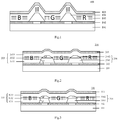
- an OLED array substrate 100 comprises a substrate 101, a first electrode layer 102, a pixel definition layer 104, an organic material functional layer 103, and a second electrode layer 105 arranged successively in a light exit direction.
- the organic material functional layer 103 comprises a light-emitting region B that emits blue light, a light-emitting region G that emits green light, and a light-emitting region R that emits red light, and comprises a first functional layer, a light-emitting layer and a second functional layer arranged successively.
- the pixel definition layer 104 comprises pixel regions corresponding to the light-emitting regions B, G, R, and spacing regions arranged between adjacent pixel regions.
- the light-emitting layer is vapor deposited using a fine metal mask to form portions of the light-emitting layer corresponding to the respective light-emitting regions B, G, R, the first functional layer, the second functional layer and the second electrode layer 105 are all formed by vapor deposition using a common mask.
- the portions of the first functional layer, the second functional layer, and the second electrode layer corresponding to the respective light-emitting regions B, G, R are all connected together.
- a longitudinal current perpendicular to the OLED array substrate and a lateral current parallel to the OLED array substrate.
- this lateral current causes two other light-emitting regions to be also illuminated weakly, resulting in abnormal display.
- an OLED array substrate 200 comprises a substrate 201, a first electrode layer 202, a pixel definition layer, an organic material functional layer 203, and a second electrode layer 205 arranged successively in a light exit direction.
- the organic material functional layer 203 comprises light-emitting regions B, G, R that emit light of different colors.
- the pixel definition layer comprises pixel regions corresponding to the light-emitting regions B, G, R, and spacing regions 204 arranged between adjacent pixel regions. Each spacing region 204 is configured to electrically isolate the adjacent light-emitting regions B, G, R.
- the pixel definition layer has a mesh structure.
- the meshes of the mesh structure correspond to the pixel regions of the pixel definition layer, while the edges of the meshes correspond to the spacing regions 204.
- the spacing regions that electrically isolate adjacent light-emitting regions upon displaying a monochromatic (e.g. green) image by only illuminating a light-emitting region of a certain color (e.g. the light-emitting region G that emits green light), it is possible to prevent adjacent light-emitting regions of different colors (e.g. the light-emitting region B that emits blue light and the light-emitting region R that emits red light) from being also illuminated weakly, which results in abnormal display. As a result, the display effect of the display device can be improved.
- a monochromatic (e.g. green) image by only illuminating a light-emitting region of a certain color (e.g. the light-emitting region G that emits green light)
- adjacent light-emitting regions of different colors e.g. the light-emitting region B that emits blue light and the light-emitting region R that emits red light
- the organic material functional layer 203 comprises a first functional layer 2031, a light-emitting layer 2032, and a second functional layer 2033 arranged successively in the light exit direction
- each spacing region 204 comprises a first spacing portion 2041 and a second spacing portion 2042 arranged successively in the light exit direction.
- the first spacing portion 2041 is configured to separate portions of the first functional layer 2031 corresponding to the respective light-emitting regions from each other.
- the first spacing portion 2041 further separates portions of the light-emitting layer 2032 corresponding to the respective light-emitting regions from each other.
- the adjacent light-emitting regions are electrically isolated from each other, as long as the portions of the first functional layer corresponding to the respective light-emitting regions are separated from each other. Therefore, as compared to an implementation of separating portions of the first functional layer, the light-emitting layer and the second functional layer corresponding to the respective light-emitting regions from each other, the second functional layer 2033 corresponding to the respective light-emitting regions can be integrally formed. Consequently, the manufacturing process of such an OLED array substrate is simpler and the cost thereof is also lower.
- the angle ⁇ between a side wall of the first spacing portion 2041 and a lower surface of the first spacing portion 2041 is larger than the angle ⁇ between a side wall of the second spacing portion 2042 and a lower surface of the second spacing portion 2042.
- the angle ⁇ between the side wall of the first spacing portion 2041 and the lower surface of the first spacing portion 2041 is no less than 60 °
- the angle ⁇ between the side wall of the second spacing portion 2042 and the lower surface of the second spacing portion 2042 is no more than 30 °.
- the lateral etching rate of the material of the first spacing portion 2041 is greater than the lateral etching rate of the material of the second spacing portion 2042.
- the greater the lateral etching rate of the material is, the larger the angle formed between the side wall and the lower surface will be.
- FIG 3 illustrates a sectional view of an OLED array substrate according to another embodiment of the present disclosure.
- An OLED array substrate 300 comprises a substrate 301, a first electrode layer 302, a pixel definition layer, an organic material functional layer 303, and a second electrode layer 305 arranged successively in a light exit direction.
- the organic material functional layer 303 comprises light-emitting regions B, G, R that emit light of different colors.
- the pixel definition layer comprises pixel regions corresponding to the light-emitting regions B, G, R, and spacing regions 304 arranged between adjacent pixel regions. Each spacing region 304 is configured to electrically isolate adjacent light-emitting regions B, G, R.
- the organic material functional layer 303 comprises a first functional layer 3031, a light-emitting layer 3032, and a second functional layer 3033 arranged successively in the light exit direction
- each spacing region 304 comprises a first spacing portion 3041 and a second spacing portion 3042 arranged successively in the light exit direction.
- the first spacing portion 3041 is configured to separate portions of the first functional layer 3031 corresponding to the respective light-emitting regions from each other.
- the first spacing portion 3041 further separates portions of the light-emitting layer 3032 corresponding to the respective light-emitting regions from each other.
- the width of an upper surface of the first spacing portion 3041 is no more than the width of the lower surface of the second spacing portion 3042.
- a notch can be formed at the interface between the first spacing portion 3041 and the second spacing portion 3042, such that the separated portions of at least the first functional layer 3031 corresponding to the respective light-emitting regions can be formed simultaneously. Consequently, the manufacturing process of the OLED array substrate is simpler and the cost thereof is also lower.
- the angle ⁇ between the side wall of the first spacing portion 3041 and the lower surface of the first spacing portion 3041 may be larger than, smaller than, even equal to the angle ⁇ between the side wall of the second spacing portion 3042 and the lower surface of the second spacing portion 3042.
- the thicknesses of the first spacing portions 2041, 3041 are greater than the thicknesses of the first functional layers 2031, 3031.
- the thickness of the first spacing portion is greater than the thickness of the first functional layer, the separated portions of the first functional layer corresponding to the respective light-emitting regions can be formed simultaneously between the first spacing portions. Consequently, the manufacturing process of the OLED array substrate is simpler and the cost thereof is also lower.
- first spacing portion and the second spacing portion are schematically illustrated as a regular trapezoid in the drawings, in an alternative embodiment, the first spacing portion and the second spacing portion may take any suitable shape.
- first spacing portion and/or the second spacing portion may be in the shape of a rectangle, an inverted trapezoid, or the like.
- the first functional layer may comprise at least one of a hole injection layer, a hole transport layer and an electron barrier layer
- the second functional layer may comprise at least one of a hole barrier layer, an electron transport layer and an electron injection layer.
- the first electrode layer is an anode layer
- the second electrode layer is a cathode layer.
- the first electrode layer may be a reflective electrode layer
- the second electrode layer may be a transparent electrode layer
- the light-emitting layer may comprise an organic light-emitting layer and an optical compensation layer arranged between the organic light-emitting layer and the first functional layer.
- the optical compensation layer is configured to adjust the effective optical cavity length in the organic material functional layer so that light of different colors is emitted from the organic material functional layer at maximum light intensity.
- the present disclosure further provides an OLED display panel comprising any of the OLED array substrates described above.
- the present disclosure provides a method of manufacturing an OLED array substrate.
- the method comprises successively forming a first electrode layer, a pixel definition layer, an organic material functional layer, and a second electrode layer.
- the organic material functional layer comprises light-emitting regions that emit light of different colors.
- the pixel definition layer comprises pixel regions corresponding to the light-emitting regions and spacing regions arranged between adjacent pixel regions. Each spacing region is configured to electrically isolate adjacent light-emitting regions.
- forming the organic material functional layer may comprise successively forming a first functional layer, a light-emitting layer, and a second functional layer.
- Each spacing region comprises a first spacing portion and a second spacing portion arranged successively in a light exit direction.
- the first spacing portion is configured to separate portions of at least the first functional layer corresponding to the respective light-emitting regions from each other.
- the first spacing portion and the second spacing portion may be formed in the same layer.
- the first spacing portion and the second spacing portion may be formed in different layers.
Landscapes
- Physics & Mathematics (AREA)
- Engineering & Computer Science (AREA)
- Optics & Photonics (AREA)
- Microelectronics & Electronic Packaging (AREA)
- Manufacturing & Machinery (AREA)
- Electromagnetism (AREA)
- Electroluminescent Light Sources (AREA)
Priority Applications (1)
| Application Number | Priority Date | Filing Date | Title |
|---|---|---|---|
| EP21187950.7A EP3923345B1 (fr) | 2016-07-29 | 2017-03-14 | Substrat de réseau de diodes delo, son procédé de fabrication, panneau d'affichage delo |
Applications Claiming Priority (2)
| Application Number | Priority Date | Filing Date | Title |
|---|---|---|---|
| CN201610609987.6A CN106158914A (zh) | 2016-07-29 | 2016-07-29 | Oled阵列基板及其制作方法、oled显示面板 |
| PCT/CN2017/076584 WO2018018895A1 (fr) | 2016-07-29 | 2017-03-14 | Substrat de réseau oled et son procédé de fabrication, et panneau d'affichage oled |
Related Child Applications (2)
| Application Number | Title | Priority Date | Filing Date |
|---|---|---|---|
| EP21187950.7A Division EP3923345B1 (fr) | 2016-07-29 | 2017-03-14 | Substrat de réseau de diodes delo, son procédé de fabrication, panneau d'affichage delo |
| EP21187950.7A Division-Into EP3923345B1 (fr) | 2016-07-29 | 2017-03-14 | Substrat de réseau de diodes delo, son procédé de fabrication, panneau d'affichage delo |
Publications (3)
| Publication Number | Publication Date |
|---|---|
| EP3493263A1 true EP3493263A1 (fr) | 2019-06-05 |
| EP3493263A4 EP3493263A4 (fr) | 2020-03-25 |
| EP3493263B1 EP3493263B1 (fr) | 2021-09-15 |
Family
ID=57327639
Family Applications (2)
| Application Number | Title | Priority Date | Filing Date |
|---|---|---|---|
| EP21187950.7A Active EP3923345B1 (fr) | 2016-07-29 | 2017-03-14 | Substrat de réseau de diodes delo, son procédé de fabrication, panneau d'affichage delo |
| EP17784824.9A Active EP3493263B1 (fr) | 2016-07-29 | 2017-03-14 | Substrat de réseau oled et son procédé de fabrication, et panneau d'affichage oled |
Family Applications Before (1)
| Application Number | Title | Priority Date | Filing Date |
|---|---|---|---|
| EP21187950.7A Active EP3923345B1 (fr) | 2016-07-29 | 2017-03-14 | Substrat de réseau de diodes delo, son procédé de fabrication, panneau d'affichage delo |
Country Status (4)
| Country | Link |
|---|---|
| US (1) | US10319794B2 (fr) |
| EP (2) | EP3923345B1 (fr) |
| CN (2) | CN106158914A (fr) |
| WO (1) | WO2018018895A1 (fr) |
Families Citing this family (10)
| Publication number | Priority date | Publication date | Assignee | Title |
|---|---|---|---|---|
| CN106158914A (zh) | 2016-07-29 | 2016-11-23 | 京东方科技集团股份有限公司 | Oled阵列基板及其制作方法、oled显示面板 |
| CN107968106A (zh) * | 2017-05-11 | 2018-04-27 | 广东聚华印刷显示技术有限公司 | Oled显示面板及其制作方法和应用 |
| WO2019109258A1 (fr) * | 2017-12-05 | 2019-06-13 | 深圳市柔宇科技有限公司 | Dispositif à delo à gamme de couleurs élevée |
| TWI673541B (zh) * | 2018-05-23 | 2019-10-01 | 友達光電股份有限公司 | 顯示面板及彩色陣列基板 |
| CN109103235B (zh) * | 2018-09-25 | 2022-11-18 | 京东方科技集团股份有限公司 | 有机发光二极管显示面板及其制作方法、显示装置 |
| CN109860272B (zh) * | 2019-04-17 | 2021-01-29 | 京东方科技集团股份有限公司 | 显示基板、显示装置 |
| WO2021035419A1 (fr) * | 2019-08-23 | 2021-03-04 | 京东方科技集团股份有限公司 | Substrat d'affichage et son procédé de fabrication |
| CN111026289B (zh) * | 2019-11-29 | 2023-07-14 | 北京空间技术研制试验中心 | 用于载人航天器的人机交互终端 |
| CN112614828B (zh) * | 2020-12-15 | 2022-10-14 | 昆山国显光电有限公司 | 显示面板及其制作方法 |
| WO2025138026A1 (fr) * | 2023-12-28 | 2025-07-03 | 京东方科技集团股份有限公司 | Substrat d'affichage et appareil d'affichage |
Family Cites Families (15)
| Publication number | Priority date | Publication date | Assignee | Title |
|---|---|---|---|---|
| TW420964B (en) | 1998-02-25 | 2001-02-01 | Toppan Printing Co Ltd | Organic electroluminescence display substrate, method of manufacturing it and organic electroluminescent display element |
| US7098060B2 (en) | 2002-09-06 | 2006-08-29 | E.I. Du Pont De Nemours And Company | Methods for producing full-color organic electroluminescent devices |
| GB0517195D0 (en) * | 2005-08-23 | 2005-09-28 | Cambridge Display Tech Ltd | Molecular electronic device structures and fabrication methods |
| JP5256605B2 (ja) | 2006-01-18 | 2013-08-07 | 凸版印刷株式会社 | 有機エレクトロルミネッセンス素子の製造方法 |
| JP2008235033A (ja) * | 2007-03-20 | 2008-10-02 | Toshiba Matsushita Display Technology Co Ltd | 表示装置及び表示装置の製造方法 |
| GB2458454B (en) | 2008-03-14 | 2011-03-16 | Cambridge Display Tech Ltd | Electronic devices and methods of making the same using solution processing techniques |
| JP2010282899A (ja) * | 2009-06-05 | 2010-12-16 | Panasonic Corp | 有機elデバイスおよびその製造方法 |
| US9240435B2 (en) | 2009-06-11 | 2016-01-19 | Joled Inc | Organic EL display |
| KR101941178B1 (ko) * | 2012-09-28 | 2019-01-23 | 삼성디스플레이 주식회사 | 유기 발광 표시 장치 및 유기 발광 표시 장치의 제조 방법 |
| CN103915571A (zh) | 2014-01-27 | 2014-07-09 | 上海天马有机发光显示技术有限公司 | 一种amoled显示面板及膜层制作方法、显示装置 |
| KR20150135722A (ko) * | 2014-05-23 | 2015-12-03 | 삼성디스플레이 주식회사 | 유기발광 디스플레이 장치 및 그 제조방법 |
| KR20150141338A (ko) * | 2014-06-10 | 2015-12-18 | 엘지디스플레이 주식회사 | 유기 발광 표시 장치 및 이의 제조 방법 |
| CN105742311B (zh) | 2014-12-11 | 2018-11-13 | 昆山国显光电有限公司 | 一种显示装置及其制备方法 |
| CN104538559B (zh) * | 2014-12-31 | 2017-10-10 | 北京维信诺科技有限公司 | 一种具有rgb像素区的有机电致发光显示装置 |
| CN106158914A (zh) | 2016-07-29 | 2016-11-23 | 京东方科技集团股份有限公司 | Oled阵列基板及其制作方法、oled显示面板 |
-
2016
- 2016-07-29 CN CN201610609987.6A patent/CN106158914A/zh active Pending
- 2016-07-29 CN CN202011053169.5A patent/CN112117318B/zh active Active
-
2017
- 2017-03-14 EP EP21187950.7A patent/EP3923345B1/fr active Active
- 2017-03-14 US US15/568,990 patent/US10319794B2/en active Active
- 2017-03-14 WO PCT/CN2017/076584 patent/WO2018018895A1/fr not_active Ceased
- 2017-03-14 EP EP17784824.9A patent/EP3493263B1/fr active Active
Also Published As
| Publication number | Publication date |
|---|---|
| CN106158914A (zh) | 2016-11-23 |
| US20180286932A1 (en) | 2018-10-04 |
| CN112117318A (zh) | 2020-12-22 |
| EP3493263A4 (fr) | 2020-03-25 |
| CN112117318B (zh) | 2024-11-01 |
| EP3923345A1 (fr) | 2021-12-15 |
| US10319794B2 (en) | 2019-06-11 |
| EP3923345B1 (fr) | 2025-10-29 |
| EP3493263B1 (fr) | 2021-09-15 |
| WO2018018895A1 (fr) | 2018-02-01 |
Similar Documents
| Publication | Publication Date | Title |
|---|---|---|
| US10319794B2 (en) | OLED array substrate, manufacturing method thereof, OLED display panel | |
| US10686018B2 (en) | Display device and manufacturing method thereof | |
| EP3236463B1 (fr) | Afficheur électroluminescent organique | |
| US9761641B2 (en) | Color filter substrate and method for manufacturing the same, OLED display panel and display apparatus | |
| US9614017B2 (en) | AMOLED backplane structure and manufacturing method thereof | |
| US10707433B2 (en) | Display panel, method of manufacturing the same, and display device | |
| US9978824B2 (en) | Organic light emitting display device | |
| CN107146804B (zh) | 有机发光二极管像素结构及有机发光二极管显示装置 | |
| US20190386074A1 (en) | Amoled display panel and amoled display | |
| US20070222354A1 (en) | Carbon nanotube field emitting display | |
| US9761639B2 (en) | Organic light emitting diode array substrate, and display device | |
| CN106796769A (zh) | 显示装置 | |
| KR20110021090A (ko) | 유기전계 발광소자 제조 용 쉐도우 마스크 | |
| US12150363B2 (en) | Display panel, display screen and display device having larger viewing angle | |
| US20070200495A1 (en) | Organic electroluminescence display device | |
| US20250081784A1 (en) | Pixel structure, display panel and display apparatus | |
| CN110265431A (zh) | 有机发光显示设备 | |
| US10325961B2 (en) | Electroluminescent display, manufacture method thereof, and display device | |
| CN110098232A (zh) | Oled显示面板 | |
| WO2017198074A1 (fr) | Source de rétroéclairage et procédé de fabrication associé, substrat d'affichage, et appareil d'affichage et procédé d'affichage associé | |
| WO2019238038A1 (fr) | Panneau d'affichage à diodes électroluminescentes organiques, son procédé de fabrication et dispositif d'affichage | |
| US12476226B1 (en) | Display device having light emitting element in concave portion of insulating substrate | |
| KR102858657B1 (ko) | 발광표시패널 및 이를 이용한 발광표시장치 | |
| TWI491036B (zh) | Organic EL display device |
Legal Events
| Date | Code | Title | Description |
|---|---|---|---|
| STAA | Information on the status of an ep patent application or granted ep patent |
Free format text: STATUS: UNKNOWN |
|
| STAA | Information on the status of an ep patent application or granted ep patent |
Free format text: STATUS: THE INTERNATIONAL PUBLICATION HAS BEEN MADE |
|
| PUAI | Public reference made under article 153(3) epc to a published international application that has entered the european phase |
Free format text: ORIGINAL CODE: 0009012 |
|
| STAA | Information on the status of an ep patent application or granted ep patent |
Free format text: STATUS: REQUEST FOR EXAMINATION WAS MADE |
|
| 17P | Request for examination filed |
Effective date: 20171027 |
|
| AK | Designated contracting states |
Kind code of ref document: A1 Designated state(s): AL AT BE BG CH CY CZ DE DK EE ES FI FR GB GR HR HU IE IS IT LI LT LU LV MC MK MT NL NO PL PT RO RS SE SI SK SM TR |
|
| AX | Request for extension of the european patent |
Extension state: BA ME |
|
| DAV | Request for validation of the european patent (deleted) | ||
| DAX | Request for extension of the european patent (deleted) | ||
| A4 | Supplementary search report drawn up and despatched |
Effective date: 20200220 |
|
| RIC1 | Information provided on ipc code assigned before grant |
Ipc: H01L 51/56 20060101ALI20200215BHEP Ipc: H01L 27/32 20060101AFI20200215BHEP |
|
| GRAP | Despatch of communication of intention to grant a patent |
Free format text: ORIGINAL CODE: EPIDOSNIGR1 |
|
| STAA | Information on the status of an ep patent application or granted ep patent |
Free format text: STATUS: GRANT OF PATENT IS INTENDED |
|
| INTG | Intention to grant announced |
Effective date: 20210324 |
|
| GRAS | Grant fee paid |
Free format text: ORIGINAL CODE: EPIDOSNIGR3 |
|
| GRAA | (expected) grant |
Free format text: ORIGINAL CODE: 0009210 |
|
| STAA | Information on the status of an ep patent application or granted ep patent |
Free format text: STATUS: THE PATENT HAS BEEN GRANTED |
|
| AK | Designated contracting states |
Kind code of ref document: B1 Designated state(s): AL AT BE BG CH CY CZ DE DK EE ES FI FR GB GR HR HU IE IS IT LI LT LU LV MC MK MT NL NO PL PT RO RS SE SI SK SM TR |
|
| REG | Reference to a national code |
Ref country code: CH Ref legal event code: EP |
|
| REG | Reference to a national code |
Ref country code: DE Ref legal event code: R096 Ref document number: 602017046107 Country of ref document: DE |
|
| REG | Reference to a national code |
Ref country code: IE Ref legal event code: FG4D |
|
| REG | Reference to a national code |
Ref country code: AT Ref legal event code: REF Ref document number: 1431196 Country of ref document: AT Kind code of ref document: T Effective date: 20211015 |
|
| REG | Reference to a national code |
Ref country code: LT Ref legal event code: MG9D |
|
| REG | Reference to a national code |
Ref country code: NL Ref legal event code: MP Effective date: 20210915 |
|
| PG25 | Lapsed in a contracting state [announced via postgrant information from national office to epo] |
Ref country code: LT Free format text: LAPSE BECAUSE OF FAILURE TO SUBMIT A TRANSLATION OF THE DESCRIPTION OR TO PAY THE FEE WITHIN THE PRESCRIBED TIME-LIMIT Effective date: 20210915 Ref country code: BG Free format text: LAPSE BECAUSE OF FAILURE TO SUBMIT A TRANSLATION OF THE DESCRIPTION OR TO PAY THE FEE WITHIN THE PRESCRIBED TIME-LIMIT Effective date: 20211215 Ref country code: NO Free format text: LAPSE BECAUSE OF FAILURE TO SUBMIT A TRANSLATION OF THE DESCRIPTION OR TO PAY THE FEE WITHIN THE PRESCRIBED TIME-LIMIT Effective date: 20211215 Ref country code: FI Free format text: LAPSE BECAUSE OF FAILURE TO SUBMIT A TRANSLATION OF THE DESCRIPTION OR TO PAY THE FEE WITHIN THE PRESCRIBED TIME-LIMIT Effective date: 20210915 Ref country code: SE Free format text: LAPSE BECAUSE OF FAILURE TO SUBMIT A TRANSLATION OF THE DESCRIPTION OR TO PAY THE FEE WITHIN THE PRESCRIBED TIME-LIMIT Effective date: 20210915 Ref country code: RS Free format text: LAPSE BECAUSE OF FAILURE TO SUBMIT A TRANSLATION OF THE DESCRIPTION OR TO PAY THE FEE WITHIN THE PRESCRIBED TIME-LIMIT Effective date: 20210915 Ref country code: HR Free format text: LAPSE BECAUSE OF FAILURE TO SUBMIT A TRANSLATION OF THE DESCRIPTION OR TO PAY THE FEE WITHIN THE PRESCRIBED TIME-LIMIT Effective date: 20210915 |
|
| REG | Reference to a national code |
Ref country code: AT Ref legal event code: MK05 Ref document number: 1431196 Country of ref document: AT Kind code of ref document: T Effective date: 20210915 |
|
| PG25 | Lapsed in a contracting state [announced via postgrant information from national office to epo] |
Ref country code: LV Free format text: LAPSE BECAUSE OF FAILURE TO SUBMIT A TRANSLATION OF THE DESCRIPTION OR TO PAY THE FEE WITHIN THE PRESCRIBED TIME-LIMIT Effective date: 20210915 Ref country code: GR Free format text: LAPSE BECAUSE OF FAILURE TO SUBMIT A TRANSLATION OF THE DESCRIPTION OR TO PAY THE FEE WITHIN THE PRESCRIBED TIME-LIMIT Effective date: 20211216 |
|
| PG25 | Lapsed in a contracting state [announced via postgrant information from national office to epo] |
Ref country code: AT Free format text: LAPSE BECAUSE OF FAILURE TO SUBMIT A TRANSLATION OF THE DESCRIPTION OR TO PAY THE FEE WITHIN THE PRESCRIBED TIME-LIMIT Effective date: 20210915 |
|
| PG25 | Lapsed in a contracting state [announced via postgrant information from national office to epo] |
Ref country code: IS Free format text: LAPSE BECAUSE OF FAILURE TO SUBMIT A TRANSLATION OF THE DESCRIPTION OR TO PAY THE FEE WITHIN THE PRESCRIBED TIME-LIMIT Effective date: 20220115 Ref country code: SM Free format text: LAPSE BECAUSE OF FAILURE TO SUBMIT A TRANSLATION OF THE DESCRIPTION OR TO PAY THE FEE WITHIN THE PRESCRIBED TIME-LIMIT Effective date: 20210915 Ref country code: SK Free format text: LAPSE BECAUSE OF FAILURE TO SUBMIT A TRANSLATION OF THE DESCRIPTION OR TO PAY THE FEE WITHIN THE PRESCRIBED TIME-LIMIT Effective date: 20210915 Ref country code: RO Free format text: LAPSE BECAUSE OF FAILURE TO SUBMIT A TRANSLATION OF THE DESCRIPTION OR TO PAY THE FEE WITHIN THE PRESCRIBED TIME-LIMIT Effective date: 20210915 Ref country code: PT Free format text: LAPSE BECAUSE OF FAILURE TO SUBMIT A TRANSLATION OF THE DESCRIPTION OR TO PAY THE FEE WITHIN THE PRESCRIBED TIME-LIMIT Effective date: 20220117 Ref country code: PL Free format text: LAPSE BECAUSE OF FAILURE TO SUBMIT A TRANSLATION OF THE DESCRIPTION OR TO PAY THE FEE WITHIN THE PRESCRIBED TIME-LIMIT Effective date: 20210915 Ref country code: NL Free format text: LAPSE BECAUSE OF FAILURE TO SUBMIT A TRANSLATION OF THE DESCRIPTION OR TO PAY THE FEE WITHIN THE PRESCRIBED TIME-LIMIT Effective date: 20210915 Ref country code: ES Free format text: LAPSE BECAUSE OF FAILURE TO SUBMIT A TRANSLATION OF THE DESCRIPTION OR TO PAY THE FEE WITHIN THE PRESCRIBED TIME-LIMIT Effective date: 20210915 Ref country code: EE Free format text: LAPSE BECAUSE OF FAILURE TO SUBMIT A TRANSLATION OF THE DESCRIPTION OR TO PAY THE FEE WITHIN THE PRESCRIBED TIME-LIMIT Effective date: 20210915 Ref country code: CZ Free format text: LAPSE BECAUSE OF FAILURE TO SUBMIT A TRANSLATION OF THE DESCRIPTION OR TO PAY THE FEE WITHIN THE PRESCRIBED TIME-LIMIT Effective date: 20210915 Ref country code: AL Free format text: LAPSE BECAUSE OF FAILURE TO SUBMIT A TRANSLATION OF THE DESCRIPTION OR TO PAY THE FEE WITHIN THE PRESCRIBED TIME-LIMIT Effective date: 20210915 |
|
| REG | Reference to a national code |
Ref country code: DE Ref legal event code: R097 Ref document number: 602017046107 Country of ref document: DE |
|
| PLBE | No opposition filed within time limit |
Free format text: ORIGINAL CODE: 0009261 |
|
| STAA | Information on the status of an ep patent application or granted ep patent |
Free format text: STATUS: NO OPPOSITION FILED WITHIN TIME LIMIT |
|
| PG25 | Lapsed in a contracting state [announced via postgrant information from national office to epo] |
Ref country code: DK Free format text: LAPSE BECAUSE OF FAILURE TO SUBMIT A TRANSLATION OF THE DESCRIPTION OR TO PAY THE FEE WITHIN THE PRESCRIBED TIME-LIMIT Effective date: 20210915 |
|
| 26N | No opposition filed |
Effective date: 20220616 |
|
| PG25 | Lapsed in a contracting state [announced via postgrant information from national office to epo] |
Ref country code: SI Free format text: LAPSE BECAUSE OF FAILURE TO SUBMIT A TRANSLATION OF THE DESCRIPTION OR TO PAY THE FEE WITHIN THE PRESCRIBED TIME-LIMIT Effective date: 20210915 |
|
| PG25 | Lapsed in a contracting state [announced via postgrant information from national office to epo] |
Ref country code: MC Free format text: LAPSE BECAUSE OF FAILURE TO SUBMIT A TRANSLATION OF THE DESCRIPTION OR TO PAY THE FEE WITHIN THE PRESCRIBED TIME-LIMIT Effective date: 20210915 |
|
| REG | Reference to a national code |
Ref country code: CH Ref legal event code: PL |
|
| REG | Reference to a national code |
Ref country code: DE Ref legal event code: R079 Ref document number: 602017046107 Country of ref document: DE Free format text: PREVIOUS MAIN CLASS: H01L0027320000 Ipc: H10K0059000000 |
|
| REG | Reference to a national code |
Ref country code: BE Ref legal event code: MM Effective date: 20220331 |
|
| PG25 | Lapsed in a contracting state [announced via postgrant information from national office to epo] |
Ref country code: LU Free format text: LAPSE BECAUSE OF NON-PAYMENT OF DUE FEES Effective date: 20220314 Ref country code: LI Free format text: LAPSE BECAUSE OF NON-PAYMENT OF DUE FEES Effective date: 20220331 Ref country code: IT Free format text: LAPSE BECAUSE OF FAILURE TO SUBMIT A TRANSLATION OF THE DESCRIPTION OR TO PAY THE FEE WITHIN THE PRESCRIBED TIME-LIMIT Effective date: 20210915 Ref country code: IE Free format text: LAPSE BECAUSE OF NON-PAYMENT OF DUE FEES Effective date: 20220314 Ref country code: FR Free format text: LAPSE BECAUSE OF NON-PAYMENT OF DUE FEES Effective date: 20220331 Ref country code: CH Free format text: LAPSE BECAUSE OF NON-PAYMENT OF DUE FEES Effective date: 20220331 |
|
| PG25 | Lapsed in a contracting state [announced via postgrant information from national office to epo] |
Ref country code: BE Free format text: LAPSE BECAUSE OF NON-PAYMENT OF DUE FEES Effective date: 20220331 |
|
| PG25 | Lapsed in a contracting state [announced via postgrant information from national office to epo] |
Ref country code: HU Free format text: LAPSE BECAUSE OF FAILURE TO SUBMIT A TRANSLATION OF THE DESCRIPTION OR TO PAY THE FEE WITHIN THE PRESCRIBED TIME-LIMIT; INVALID AB INITIO Effective date: 20170314 |
|
| PG25 | Lapsed in a contracting state [announced via postgrant information from national office to epo] |
Ref country code: MK Free format text: LAPSE BECAUSE OF FAILURE TO SUBMIT A TRANSLATION OF THE DESCRIPTION OR TO PAY THE FEE WITHIN THE PRESCRIBED TIME-LIMIT Effective date: 20210915 Ref country code: CY Free format text: LAPSE BECAUSE OF FAILURE TO SUBMIT A TRANSLATION OF THE DESCRIPTION OR TO PAY THE FEE WITHIN THE PRESCRIBED TIME-LIMIT Effective date: 20210915 |
|
| PG25 | Lapsed in a contracting state [announced via postgrant information from national office to epo] |
Ref country code: TR Free format text: LAPSE BECAUSE OF FAILURE TO SUBMIT A TRANSLATION OF THE DESCRIPTION OR TO PAY THE FEE WITHIN THE PRESCRIBED TIME-LIMIT Effective date: 20210915 |
|
| PG25 | Lapsed in a contracting state [announced via postgrant information from national office to epo] |
Ref country code: MT Free format text: LAPSE BECAUSE OF FAILURE TO SUBMIT A TRANSLATION OF THE DESCRIPTION OR TO PAY THE FEE WITHIN THE PRESCRIBED TIME-LIMIT Effective date: 20210915 |
|
| PGFP | Annual fee paid to national office [announced via postgrant information from national office to epo] |
Ref country code: GB Payment date: 20260324 Year of fee payment: 10 |
|
| PGFP | Annual fee paid to national office [announced via postgrant information from national office to epo] |
Ref country code: DE Payment date: 20260319 Year of fee payment: 10 |