EP3496129B1 - Microscope à particules chargées de transmission comportant un module eels/eftem amélioré - Google Patents
Microscope à particules chargées de transmission comportant un module eels/eftem amélioré Download PDFInfo
- Publication number
- EP3496129B1 EP3496129B1 EP17205782.0A EP17205782A EP3496129B1 EP 3496129 B1 EP3496129 B1 EP 3496129B1 EP 17205782 A EP17205782 A EP 17205782A EP 3496129 B1 EP3496129 B1 EP 3496129B1
- Authority
- EP
- European Patent Office
- Prior art keywords
- quadrupoles
- plane
- energy
- quadrupole
- slit
- Prior art date
- Legal status (The legal status is an assumption and is not a legal conclusion. Google has not performed a legal analysis and makes no representation as to the accuracy of the status listed.)
- Active
Links
Images


Classifications
-
- H—ELECTRICITY
- H01—ELECTRIC ELEMENTS
- H01J—ELECTRIC DISCHARGE TUBES OR DISCHARGE LAMPS
- H01J37/00—Discharge tubes with provision for introducing objects or material to be exposed to the discharge, e.g. for the purpose of examination or processing thereof
- H01J37/02—Details
- H01J37/04—Arrangements of electrodes and associated parts for generating or controlling the discharge, e.g. electron-optical arrangement or ion-optical arrangement
- H01J37/05—Electron or ion-optical arrangements for separating electrons or ions according to their energy or mass
-
- H—ELECTRICITY
- H01—ELECTRIC ELEMENTS
- H01J—ELECTRIC DISCHARGE TUBES OR DISCHARGE LAMPS
- H01J37/00—Discharge tubes with provision for introducing objects or material to be exposed to the discharge, e.g. for the purpose of examination or processing thereof
- H01J37/02—Details
- H01J37/04—Arrangements of electrodes and associated parts for generating or controlling the discharge, e.g. electron-optical arrangement or ion-optical arrangement
- H01J37/10—Lenses
-
- H—ELECTRICITY
- H01—ELECTRIC ELEMENTS
- H01J—ELECTRIC DISCHARGE TUBES OR DISCHARGE LAMPS
- H01J37/00—Discharge tubes with provision for introducing objects or material to be exposed to the discharge, e.g. for the purpose of examination or processing thereof
- H01J37/02—Details
- H01J37/04—Arrangements of electrodes and associated parts for generating or controlling the discharge, e.g. electron-optical arrangement or ion-optical arrangement
- H01J37/147—Arrangements for directing or deflecting the discharge along a desired path
-
- H—ELECTRICITY
- H01—ELECTRIC ELEMENTS
- H01J—ELECTRIC DISCHARGE TUBES OR DISCHARGE LAMPS
- H01J37/00—Discharge tubes with provision for introducing objects or material to be exposed to the discharge, e.g. for the purpose of examination or processing thereof
- H01J37/02—Details
- H01J37/21—Means for adjusting the focus
-
- H—ELECTRICITY
- H01—ELECTRIC ELEMENTS
- H01J—ELECTRIC DISCHARGE TUBES OR DISCHARGE LAMPS
- H01J37/00—Discharge tubes with provision for introducing objects or material to be exposed to the discharge, e.g. for the purpose of examination or processing thereof
- H01J37/02—Details
- H01J37/22—Optical, image processing or photographic arrangements associated with the tube
- H01J37/226—Optical arrangements for illuminating the object; optical arrangements for collecting light from the object
-
- H—ELECTRICITY
- H01—ELECTRIC ELEMENTS
- H01J—ELECTRIC DISCHARGE TUBES OR DISCHARGE LAMPS
- H01J37/00—Discharge tubes with provision for introducing objects or material to be exposed to the discharge, e.g. for the purpose of examination or processing thereof
- H01J37/26—Electron or ion microscopes; Electron or ion diffraction tubes
- H01J37/261—Details
- H01J37/263—Contrast, resolution or power of penetration
-
- H—ELECTRICITY
- H01—ELECTRIC ELEMENTS
- H01J—ELECTRIC DISCHARGE TUBES OR DISCHARGE LAMPS
- H01J37/00—Discharge tubes with provision for introducing objects or material to be exposed to the discharge, e.g. for the purpose of examination or processing thereof
- H01J37/26—Electron or ion microscopes; Electron or ion diffraction tubes
- H01J37/261—Details
- H01J37/265—Controlling the tube; circuit arrangements adapted to a particular application not otherwise provided, e.g. bright-field-dark-field illumination
-
- H—ELECTRICITY
- H01—ELECTRIC ELEMENTS
- H01J—ELECTRIC DISCHARGE TUBES OR DISCHARGE LAMPS
- H01J49/00—Particle spectrometers or separator tubes
- H01J49/02—Details
- H01J49/06—Electron- or ion-optical arrangements
- H01J49/062—Ion guides
- H01J49/063—Multipole ion guides, e.g. quadrupoles, hexapoles
-
- H—ELECTRICITY
- H01—ELECTRIC ELEMENTS
- H01J—ELECTRIC DISCHARGE TUBES OR DISCHARGE LAMPS
- H01J49/00—Particle spectrometers or separator tubes
- H01J49/44—Energy spectrometers, e.g. alpha-, beta-spectrometers
-
- H—ELECTRICITY
- H01—ELECTRIC ELEMENTS
- H01J—ELECTRIC DISCHARGE TUBES OR DISCHARGE LAMPS
- H01J2237/00—Discharge tubes exposing object to beam, e.g. for analysis treatment, etching, imaging
- H01J2237/05—Arrangements for energy or mass analysis
- H01J2237/057—Energy or mass filtering
-
- H—ELECTRICITY
- H01—ELECTRIC ELEMENTS
- H01J—ELECTRIC DISCHARGE TUBES OR DISCHARGE LAMPS
- H01J2237/00—Discharge tubes exposing object to beam, e.g. for analysis treatment, etching, imaging
- H01J2237/153—Correcting image defects, e.g. stigmators
- H01J2237/1534—Aberrations
-
- H—ELECTRICITY
- H01—ELECTRIC ELEMENTS
- H01J—ELECTRIC DISCHARGE TUBES OR DISCHARGE LAMPS
- H01J2237/00—Discharge tubes exposing object to beam, e.g. for analysis treatment, etching, imaging
- H01J2237/244—Detection characterized by the detecting means
- H01J2237/24485—Energy spectrometers
-
- H—ELECTRICITY
- H01—ELECTRIC ELEMENTS
- H01J—ELECTRIC DISCHARGE TUBES OR DISCHARGE LAMPS
- H01J2237/00—Discharge tubes exposing object to beam, e.g. for analysis treatment, etching, imaging
- H01J2237/26—Electron or ion microscopes
- H01J2237/28—Scanning microscopes
- H01J2237/2802—Transmission microscopes
Definitions
- the invention relates to a method of using a Transmission Charged Particle Microscope comprising:
- the invention also relates to a Transmission Charged Particle Microscope in which such a method can be enacted.
- An EELS/EFTEM module as alluded to here is sometimes embodied as a so-called Post-Column Filter (PCF), though this does not necessarily have to be the case.
- PCF Post-Column Filter
- Charged-particle microscopy is a well-known and increasingly important technique for imaging microscopic objects, particularly in the form of electron microscopy.
- the basic genus of electron microscope has undergone evolution into a number of well-known apparatus species, such as the Transmission Electron Microscope (TEM), Scanning Electron Microscope (SEM), and Scanning Transmission Electron Microscope (STEM), and also into various sub-species, such as so-called “dual-beam” apparatus (e.g . a FIB-SEM), which additionally employ a "machining" Focused Ion Beam (FIB), allowing supportive activities such as ion-beam milling or lon-Beam-Induced Deposition (IBID), for example. More specifically:
- charged particle microscopy can also be performed using other species of charged particle.
- charged particle should be broadly interpreted as encompassing electrons, positive ions (e.g . Ga or He ions), negative ions (such as oxygen), protons and positrons, for instance.
- positive ions e.g . Ga or He ions
- negative ions such as oxygen
- protons e.g., protons
- positrons e.g., oxygen
- references such as the following:
- a charged particle microscope may also have other functionalities, such as performing spectroscopy, examining diffractograms, studying ion channeling / ion backscattering (Rutherford Backscattering Spectrometry), etc .
- TCPM Transmission Charged Particle Microscope
- An EELS/EFTEM module as referred to here will generally comprise:
- the employed sensing device may be unitary or compound/distributed in nature, and can take many different forms, depending on what it is intended to sense. It may, for example, comprise one or more photodiodes, CMOS detectors, CCD detectors, photovoltaic cells, etc.
- EELS is a technique used in (S)TEMs to obtain elemental/chemical information pertaining to a given specimen.
- a moving electron in an irradiating beam (from the (S)TEM's illuminator) can transfer energy to a bound electron in a core shell of an atom in the specimen, and promote this core electron to an outer shell (inelastic scattering).
- This energy transfer from the moving electron gives rise to a so-called "core-loss peak" (CLP) in the EELS spectrum.
- the (coarse) position (in energy units) of the CLP is element-specific, and its precise position and shape are specific to the element's chemical environment and bonding.
- an EELS spectrum will generally also contain so-called “Plasmon Resonance Peaks” (PRPs), i.e. a relatively broad series of peaks/shoulders associated with single or multiple scattering of electrons on plasmons in the specimen. These PRPs typically lie in the energy range 0-50 eV.
- EELS modules can also be used as energy-selective imaging devices (EFTEM functionality). To achieve this, they employ a slit ("letterbox”) at/proximal their (primary) spectrum plane.
- this slit When the module is used as a pure spectrometer, this slit is retracted, and the spectrum plane can be magnified and imaged onto the employed detector (camera) using post-dispersion optics.
- the slit can be invoked to pass/admit only a specific energy window (typically of the order of 10-50eV wide); in that case, the post-dispersion (post-slit) optics then image a Fourier Transform plane of said spectrum plane onto the employed detector.
- various quadrupoles are employed to magnify and focus the dispersion produced by the dispersing device (prism).
- the skilled artisan will realize that these quadrupoles have inherent and parasitic aberrations, such as chromatic aberrations (caused by the dependence of the focusing power of the quadrupoles on the energy of the electrons in the beam) and higher-order aberrations caused by the non-zero length/thickness of the quadrupoles and by fringe fields at the entrance and exit of the quadrupoles.
- the dispersing device also has inherent and parasitic aberrations. In order to address such aberrations, it is conventional to employ one or more dedicated "clean-up" multipole fields (e.g .
- E the primary (input) beam energy (typically somewhere between 20keV and 1000keV)
- m the electron mass
- c the speed of light
- ⁇ E the detected spectral energy spread
- the invention exploits the insight that, by maintaining off-axis non-dispersive rays vicinal to the Z-axis in the "post-slit" space between the slit plane and image plane, one can suffice with excitation of a minimal number of quadrupoles in said post-slit space - ideally just one quadrupole, but excitation of a pair of adjacent quadrupoles is also a possibility (see below). Although there may be more than two quadrupoles present in the second quadrupole series (see the aforementioned US 2017/0125210 A1 , for example, and also Figures 3A-3C below), the invention only needs to excite a single one / single adjacent pair of these at any given time.
- this embodiment uses a geometric recipe to determine which post-slit quadrupoles are best excited in a given situation.
- the position of intersection point p along the Z-axis will be influenced by the particular details of the selected excitation of the first-series / "pre-slit” quadrupoles, since this determines the "focal length" of the pre-slit optics.
- both quadrupoles Qa, Qb can be excited with the same polarity ( e.g. positive); alternatively, one could, for example, choose a scenario whereby e a ⁇ +100% and e b ⁇ -10%, for instance, which still results in a (strong) net positive excitation
- the energy-dispersed beam is de-magnified between said dispersing device and slit plane. In essence, this ensures that, after leaving the dispersion device, the dispersed beam will fit within the confines of the apparatus that has yet to be traversed, particularly:
- the inventors have examined various scenarios and have observed that, if the non-dispersive YZ ray enters the dispersing device at a distance d E from the optical axis, and has a maximum distance d L from the optical axis within the second quadrupole series, then the ratio d E /d L is desirably ⁇ 3, preferably ⁇ 5, and more preferably ⁇ 10. Aberrations scaling with the second (or higher) power of this ratio will be correspondingly drastically reduced.
- dispersing device used in the present invention can take various different forms, according to choice.
- it may comprise:
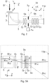
- Figure 1 (not to scale) is a highly schematic depiction of an embodiment of a TCPM M in which the present invention is implemented; more specifically, it shows an embodiment of a TEM/STEM.
- an electron source 4 produces a beam B of electrons that propagates along an electron-optical axis B' and traverses an electron-optical illuminator (charged particle beam column) 6, serving to direct/focus the electrons onto a chosen part of a specimen S (which may, for example, be (locally) thinned/planarized).
- illuminator 6 are:
- the specimen S is held on a specimen holder H that can be positioned in multiple degrees of freedom by a positioning device / stage A, which moves a cradle A' into which holder H is (removably) affixed; for example, the specimen holder H may comprise a finger that can be moved ( inter alia ) in the XY plane (see the depicted Cartesian coordinate system; typically, motion parallel to Z and tilt about X/Y will also be possible). Such movement allows different parts of the specimen S to be illuminated / imaged / inspected by the electron beam B traveling along axis B' (in the Z direction), and/or allows scanning motion to be performed as an alternative to beam scanning.
- an optional cooling device (not depicted) can be brought into intimate thermal contact with the specimen holder H, so as to maintain it (and the specimen S thereupon) at cryogenic temperatures, for example.
- the electron beam B will interact with the specimen S in such a manner as to cause various types of "stimulated” radiation to emanate from the specimen S, including (for example) secondary electrons, backscattered electrons, X-rays and optical radiation (cathodoluminescence).
- various types of "stimulated" radiation including (for example) secondary electrons, backscattered electrons, X-rays and optical radiation (cathodoluminescence).
- these radiation types can be detected with the aid of analysis device 22, which might be a combined scintillator/photomultiplier or EDX (Energy-Dispersive X-Ray Spectroscopy) module, for instance; in such a case, an image could be constructed using basically the same principle as in a SEM.
- an imaging system projection lens 24 which will generally comprise a variety of electrostatic / magnetic lenses, deflectors, correctors (such as stigmators), etc.
- this imaging system 24 can focus the transmitted electron flux onto a fluorescent screen (sensing device) 26, which, if desired, can be retracted/withdrawn (as schematically indicated by arrows 26') so as to get it out of the way of axis B'.
- An image or diffractogram of (part of) the specimen S will be formed by imaging system 24 on screen 26, and this may be viewed through viewing port 28 located in a suitable part of a wall of enclosure 2.
- the retraction mechanism for screen 26 may, for example, be mechanical and/or electrical in nature, and is not depicted here.
- spectral apparatus 34 can also be integrated into the imaging system 24.
- controller 20 is connected to various illustrated components via control lines (buses) 20'.
- This controller 20 can provide a variety of functions, such as synchronizing actions, providing setpoints, processing signals, performing calculations, and displaying messages/information on a display device (not depicted).
- the (schematically depicted) controller 20 may be (partially) inside or outside the enclosure 2, and may have a unitary or composite structure, as desired.
- the interior of the enclosure 2 does not have to be kept at a strict vacuum; for example, in a so-called "Environmental TEM/STEM", a background atmosphere of a given gas is deliberately introduced / maintained within the enclosure 2.
- the skilled artisan will also understand that, in practice, it may be advantageous to confine the volume of enclosure 2 so that, where possible, it closely encapsulates the axis B', taking the form of a small tube ( e.g . of the order of 1 cm in diameter) through which the employed electron beam passes, but widening out to accommodate structures such as the source 4, specimen holder H, screen 26, camera 30, camera 32, spectral apparatus 34, etc.
- FIG. 2 shows an enlarged and more detailed view of the spectral apparatus 34 in Figure 1 .
- flux B" of electrons (which has passed through specimen S and imaging system 24) is shown propagating along electron-optical axis B'.
- the flux B" enters a dispersing device 3 ("electron prism"), where it is dispersed (fanned out) into an energy-resolved / energy-differentiated (continuous) array 5 of spectral sub-beams (schematically indicated in Figure 2 using broken lines), which are distributed along dispersion direction X.
- pre-dispersion optics 3' which will generally comprise one or more multipole elements, for example; these may generate a hexapole field and/or quadrupole field, for example, inter alia for purposes of aberration mitigation.
- the array 5 of sub-beams encounters an adjustable/retractable slit (letterbox) 7, which can, for example, be used in EFTEM-mode to select/admit a given portion of the array 5 and to discard/occlude other portions thereof; to this end, the slit 7 is connected to an actuation device 7a that can be invoked to open / close / move the (opening in the) slit 7 as desired. In EELS mode, this slit 7 is usually (fully) open/ retracted.
- the slit 7 is advantageously disposed at a location (slit plane 7p) at or proximal to a dispersion plane of the spectral apparatus 34; similarly, detector 11 (in image plane 11p) is also advantageously located at or proximal to such a plane. If required, it is possible to aim/shift the array 5 of spectral sub-beams falling upon the slit 7 by appropriately adjusting, for example, (an electrical signal to) the dispersing device 3 and/or a drift tube / deflector (not depicted) provided between the dispersing device 3 and slit 7, for instance.
- pre-slit optics 9a and post-slit optics 9b which respectively comprise a first series and second series of quadrupoles (or, more generally formulated, multipoles capable of excitation to produce a quadrupole lensing field).
- first series and second series of quadrupoles or, more generally formulated, multipoles capable of excitation to produce a quadrupole lensing field.
- Figure 3B corresponds largely to Figure 3A , but depicts a different embodiment of the invention.
- Figure 3B corresponds largely to Figure 3A , but depicts a different embodiment of the invention.
- Figure 3C corresponds largely to Figures 3A / 3B , but depicts yet another embodiment of the invention. In this case:
Landscapes
- Chemical & Material Sciences (AREA)
- Analytical Chemistry (AREA)
- Analysing Materials By The Use Of Radiation (AREA)
Claims (7)
- Procédé d'utilisation d'un microscope à transmission à particules chargées (M) comprenant :- Un porte-échantillon (H), pour contenir un échantillon (S) ;- Une source (4), pour produire un faisceau (B) de particules chargées ;- Un illuminateur (6), pour diriger ledit faisceau (B) de manière à irradier l'échantillon (S) ;- Un système d'imagerie (24), pour recevoir un flux de particules chargées transmises à travers l'échantillon et le diriger sur un dispositif de détection ;- Un dispositif de commande (20), pour commander au moins certains aspects fonctionnels du microscope (M),dans lequel procédé le dispositif de détection est choisi pour être un module EELS/EFTEM comprenant :- Un plan d'entrée ;- Un plan d'image (11p), où en mode EELS un spectre EELS est formé et en mode EFTEM, une image EFTEM est formée ;- Un plan de fente (7p) entre ledit plan d'entrée et ledit plan d'image, où en mode EFTEM une focalisation de dispersion en énergie est formée ;- Un dispositif de dispersion (3), entre ledit plan d'entrée et ledit plan de fente, pour disperser un faisceau entrant dans un faisceau dispersé en énergie avec une direction de dispersion associée ;- Une première série de quadripôles (QI, QII) entre ledit dispositif de dispersion et ledit plan de fente ;- Une seconde série de quadripôles (Q1, Q2, Q3, Q4) entre ledit plan de fente et ledit plan d'image,lesquels dispositif de dispersion (3) et quadripôles (Q) sont agencés le long d'un axe optique, moyennant quoi, pour un système de coordonnées cartésiennes (X, Y, Z) dans lequel ledit axe optique est disposé le long de Z, ladite direction de dispersion est définie comme étant parallèle à X,caractérisé par les étapes suivantes en mode EELS :- Dans ladite première série de quadripôles (QI, QII), l'excitation d'un ou plusieurs quadripôles de manière à dévier un rayon YZ non dispersif hors axe sortant dudit dispositif de dispersion sur une trajectoire paraxiale audit axe optique depuis ledit plan de fente vers ledit plan d'image ;- Dans ladite seconde série de quadripôles (Q1, Q2, Q3, Q4), l'excitation soit :(a) D'un seul quadripôle ; ou(b) D'une paire de quadripôles adjacents,
de manière à focaliser ledit faisceau dispersé en énergie sur ledit plan d'image ;- dans lequel, pour une énergie de faisceau E et un étalement spectral d'énergie ΔE détecté, un paramètre d'énergie ΔEr/Er a une valeur > 0,0125, où :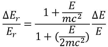
- Procédé selon la revendication 1, dans lequel :- Un rayon dispersif sur axe entrant dans ledit dispositif de dispersion (3) traverse ledit axe optique au niveau d'un point d'intersection p ;- Dans ladite seconde série de quadripôles (Q1, Q2, Q3, Q4), si ledit point d'intersection p se trouve :• À l'intérieur d'un quadripôle donné, l'option (a) est alors appliquée sur ce quadripôle ;• Entre une paire de quadripôles adjacents, l'option (b) est alors appliquée sur cette paire de quadripôles.
- Procédé selon la revendication 1 ou 2, dans lequel ladite excitation de quadripôle dans la seconde série de quadripôles satisfait sensiblement à la formule :
 - ea, eb sont des excitations efficaces respectives d'une paire de quadripôles adjacents Qa, Qb ;- da, db sont des distances axiales respectives du point d'intersection p par rapport à un centre de chacun des quadripôles Qa, Qb.
 - Procédé selon l'une quelconque des revendications 1 à 3, dans lequel, dans l'option (b), les deux quadripôles sont excités avec la même polarité.
- Procédé selon l'une quelconque des revendications 1 à 4, dans lequel ledit faisceau dispersé en énergie est désagrandi entre ledit dispositif de dispersion (3) et ledit plan de fente (7p).
- Procédé selon l'une quelconque des revendications 1 à 5, dans lequel, si ledit rayon non dispersif YZ entre dans ledit dispositif de dispersion (3) à une distance dE depuis l'axe optique, et a une distance maximale dL depuis l'axe optique à l'intérieur de la seconde série de quadripôle, puis dE/dL ≥ 3, de préférence ≥ 5, plus préférablement ≥ 10.
- Microscope à transmission à particules chargées (M) comprenant :- Un porte-échantillon (H), pour contenir un échantillon (S) ;- Une source (4), poure produire un faisceau (B) de particules chargées ;- Un illuminateur (6), pour diriger ledit faisceau (B) de manière à irradier l'échantillon (S) ;- Un système d'imagerie (24), pour recevoir un flux de particules chargées transmises à travers l'échantillon et le diriger sur un dispositif de détection ;- Un dispositif de commande (20), pour commander au moins certains aspects fonctionnels du microscope (M),dans lequel le dispositif de détection comprend un module EELS/EFTEM comprenant :- Un plan d'entrée ;- Un plan d'image (11p), où en mode EELS un spectre EELS est formé et en mode EFTEM, une image EFTEM est formée ;- Un plan de fente (7p) entre ledit plan d'entrée et ledit plan d'image, où en mode EFTEM une focalisation de dispersion en énergie est formée ;- Un dispositif de dispersion (3), entre ledit plan d'entrée et ledit plan de fente (7p), pour disperser un faisceau entrant dans un faisceau dispersé en énergie avec une direction de dispersion associée ;- Une première série de quadripôles (QI, QII) entre ledit dispositif de dispersion (3) et ledit plan de fente (7p) ;- Une seconde série de quadripôles (Q1, Q2, Q3, Q4) entre ledit plan de fente (7p) et ledit plan d'image (11p),lesquels dispositif de dispersion (3) et quadripôles sont agencés le long d'un axe optique, moyennant quoi, pour un système de coordonnées cartésiennes (X, Y, Z) dans lequel ledit axe optique est disposé le long de Z, ladite direction de dispersion est définie comme étant parallèle à X,caractérisé en ce que ledit dispositif de commande est configuré pour, en mode EELS :- Dans ladite première série de quadripôles (QI, QII), exciter un ou plusieurs quadripôles de manière à dévier un rayon YZ non dispersif hors axe sortant dudit dispositif de dispersion sur une trajectoire paraxiale audit axe optique depuis ledit plan de fente vers ledit plan d'image ;- Dans ladite seconde série de quadripôles (Q1, Q2, Q3, Q4), exciter soit :(a) Un seul quadripôle ; ou(b) Une paire de quadripôles adjacents,
de manière à focaliser ledit faisceau dispersé en énergie sur ledit plan d'image (11p) ;- dans lequel, pour une énergie de faisceau E et un étalement spectral d'énergie détecté ΔE, un paramètre d'énergie ΔEr/Er a une valeur > 0,0125, où :
Priority Applications (4)
| Application Number | Priority Date | Filing Date | Title |
|---|---|---|---|
| EP17205782.0A EP3496129B1 (fr) | 2017-12-07 | 2017-12-07 | Microscope à particules chargées de transmission comportant un module eels/eftem amélioré |
| US16/210,531 US10559448B2 (en) | 2017-12-07 | 2018-12-05 | Transmission charged particle microscope with improved EELS/EFTEM module |
| JP2018228641A JP7103926B2 (ja) | 2017-12-07 | 2018-12-06 | 改善されたeels/eftemモジュールを有する透過型荷電粒子顕微鏡およびその使用方法 |
| CN201811488218.0A CN109904053B (zh) | 2017-12-07 | 2018-12-06 | 具有改进eels/eftem模块的透射带电粒子显微镜 |
Applications Claiming Priority (1)
| Application Number | Priority Date | Filing Date | Title |
|---|---|---|---|
| EP17205782.0A EP3496129B1 (fr) | 2017-12-07 | 2017-12-07 | Microscope à particules chargées de transmission comportant un module eels/eftem amélioré |
Publications (2)
| Publication Number | Publication Date |
|---|---|
| EP3496129A1 EP3496129A1 (fr) | 2019-06-12 |
| EP3496129B1 true EP3496129B1 (fr) | 2023-11-01 |
Family
ID=60627513
Family Applications (1)
| Application Number | Title | Priority Date | Filing Date |
|---|---|---|---|
| EP17205782.0A Active EP3496129B1 (fr) | 2017-12-07 | 2017-12-07 | Microscope à particules chargées de transmission comportant un module eels/eftem amélioré |
Country Status (4)
| Country | Link |
|---|---|
| US (1) | US10559448B2 (fr) |
| EP (1) | EP3496129B1 (fr) |
| JP (1) | JP7103926B2 (fr) |
| CN (1) | CN109904053B (fr) |
Families Citing this family (3)
| Publication number | Priority date | Publication date | Assignee | Title |
|---|---|---|---|---|
| EP3889995A1 (fr) | 2020-03-31 | 2021-10-06 | FEI Company | Microscope à transmission de particules chargées comportant un détecteur de spectroscopie de perte d'énergie d'électrons |
| JP7465295B2 (ja) * | 2022-02-22 | 2024-04-10 | 日本電子株式会社 | 収差補正装置および電子顕微鏡 |
| WO2026018332A1 (fr) * | 2024-07-17 | 2026-01-22 | 株式会社日立ハイテク | Dispositif à faisceau de particules chargées et procédé d'ajustement de dispositif à faisceau de particules chargées |
Citations (1)
| Publication number | Priority date | Publication date | Assignee | Title |
|---|---|---|---|---|
| EP0917725B1 (fr) * | 1996-08-07 | 2007-06-27 | Gatan, Inc. | Reglage automatique d'un microscope electronique a transmission a filtrage d'energie |
Family Cites Families (4)
| Publication number | Priority date | Publication date | Assignee | Title |
|---|---|---|---|---|
| JP5517584B2 (ja) * | 2009-12-08 | 2014-06-11 | 株式会社日立ハイテクノロジーズ | 電子顕微鏡 |
| EP2388796A1 (fr) * | 2010-05-21 | 2011-11-23 | FEI Company | Détection simultanée d'électrons |
| EP2998979A1 (fr) * | 2014-09-22 | 2016-03-23 | Fei Company | Spectroscopie améliorée dans un système de microscope à particules chargées de transmission |
| EP3065160B1 (fr) | 2015-11-02 | 2017-12-20 | FEI Company | Colonne de montant filtre avec plage d'énergie améliorée |
-
2017
- 2017-12-07 EP EP17205782.0A patent/EP3496129B1/fr active Active
-
2018
- 2018-12-05 US US16/210,531 patent/US10559448B2/en active Active
- 2018-12-06 CN CN201811488218.0A patent/CN109904053B/zh active Active
- 2018-12-06 JP JP2018228641A patent/JP7103926B2/ja active Active
Patent Citations (1)
| Publication number | Priority date | Publication date | Assignee | Title |
|---|---|---|---|---|
| EP0917725B1 (fr) * | 1996-08-07 | 2007-06-27 | Gatan, Inc. | Reglage automatique d'un microscope electronique a transmission a filtrage d'energie |
Also Published As
| Publication number | Publication date |
|---|---|
| US10559448B2 (en) | 2020-02-11 |
| US20190180973A1 (en) | 2019-06-13 |
| CN109904053A (zh) | 2019-06-18 |
| CN109904053B (zh) | 2023-07-28 |
| JP7103926B2 (ja) | 2022-07-20 |
| JP2019102464A (ja) | 2019-06-24 |
| EP3496129A1 (fr) | 2019-06-12 |
Similar Documents
| Publication | Publication Date | Title |
|---|---|---|
| US9991087B2 (en) | Spectroscopy in a transmission charged-particle microscope | |
| US9984852B1 (en) | Time-of-flight charged particle spectroscopy | |
| EP2993683B1 (fr) | Procédé permettant de réaliser une spectroscopie dans un microscope à particules chargées de transmission | |
| US10522323B2 (en) | Electron energy loss spectroscopy with adjustable energy resolution | |
| EP3444836B1 (fr) | Détection d'un motif de diffraction dans un microscope à transmission à particules chargées | |
| US20230207254A1 (en) | Electron microscope with improved imaging resolution | |
| US10832901B2 (en) | EELS detection technique in an electron microscope | |
| EP3370247A1 (fr) | Mesure d'aberrations dans un microscope à particules chargées | |
| US11024483B2 (en) | Transmission charged particle microscope with adjustable beam energy spread | |
| JP7079135B2 (ja) | 荷電粒子顕微鏡のガンレンズ設計 | |
| US10559448B2 (en) | Transmission charged particle microscope with improved EELS/EFTEM module | |
| US11948771B2 (en) | Method of determining an energy width of a charged particle beam | |
| JP2006278069A (ja) | ウィーンフィルタ型エネルギーアナライザ及び放出電子顕微鏡 |
Legal Events
| Date | Code | Title | Description |
|---|---|---|---|
| PUAI | Public reference made under article 153(3) epc to a published international application that has entered the european phase |
Free format text: ORIGINAL CODE: 0009012 |
|
| STAA | Information on the status of an ep patent application or granted ep patent |
Free format text: STATUS: THE APPLICATION HAS BEEN PUBLISHED |
|
| AK | Designated contracting states |
Kind code of ref document: A1 Designated state(s): AL AT BE BG CH CY CZ DE DK EE ES FI FR GB GR HR HU IE IS IT LI LT LU LV MC MK MT NL NO PL PT RO RS SE SI SK SM TR |
|
| AX | Request for extension of the european patent |
Extension state: BA ME |
|
| STAA | Information on the status of an ep patent application or granted ep patent |
Free format text: STATUS: REQUEST FOR EXAMINATION WAS MADE |
|
| 17P | Request for examination filed |
Effective date: 20191023 |
|
| RBV | Designated contracting states (corrected) |
Designated state(s): AL AT BE BG CH CY CZ DE DK EE ES FI FR GB GR HR HU IE IS IT LI LT LU LV MC MK MT NL NO PL PT RO RS SE SI SK SM TR |
|
| GRAP | Despatch of communication of intention to grant a patent |
Free format text: ORIGINAL CODE: EPIDOSNIGR1 |
|
| STAA | Information on the status of an ep patent application or granted ep patent |
Free format text: STATUS: GRANT OF PATENT IS INTENDED |
|
| INTG | Intention to grant announced |
Effective date: 20230531 |
|
| GRAS | Grant fee paid |
Free format text: ORIGINAL CODE: EPIDOSNIGR3 |
|
| GRAA | (expected) grant |
Free format text: ORIGINAL CODE: 0009210 |
|
| STAA | Information on the status of an ep patent application or granted ep patent |
Free format text: STATUS: THE PATENT HAS BEEN GRANTED |
|
| AK | Designated contracting states |
Kind code of ref document: B1 Designated state(s): AL AT BE BG CH CY CZ DE DK EE ES FI FR GB GR HR HU IE IS IT LI LT LU LV MC MK MT NL NO PL PT RO RS SE SI SK SM TR |
|
| REG | Reference to a national code |
Ref country code: GB Ref legal event code: FG4D |
|
| REG | Reference to a national code |
Ref country code: CH Ref legal event code: EP |
|
| REG | Reference to a national code |
Ref country code: DE Ref legal event code: R096 Ref document number: 602017075938 Country of ref document: DE |
|
| REG | Reference to a national code |
Ref country code: IE Ref legal event code: FG4D |
|
| P01 | Opt-out of the competence of the unified patent court (upc) registered |
Effective date: 20231219 |
|
| REG | Reference to a national code |
Ref country code: LT Ref legal event code: MG9D |
|
| REG | Reference to a national code |
Ref country code: NL Ref legal event code: MP Effective date: 20231101 |
|
| PG25 | Lapsed in a contracting state [announced via postgrant information from national office to epo] |
Ref country code: GR Free format text: LAPSE BECAUSE OF FAILURE TO SUBMIT A TRANSLATION OF THE DESCRIPTION OR TO PAY THE FEE WITHIN THE PRESCRIBED TIME-LIMIT Effective date: 20240202 |
|
| PG25 | Lapsed in a contracting state [announced via postgrant information from national office to epo] |
Ref country code: IS Free format text: LAPSE BECAUSE OF FAILURE TO SUBMIT A TRANSLATION OF THE DESCRIPTION OR TO PAY THE FEE WITHIN THE PRESCRIBED TIME-LIMIT Effective date: 20240301 |
|
| PG25 | Lapsed in a contracting state [announced via postgrant information from national office to epo] |
Ref country code: LT Free format text: LAPSE BECAUSE OF FAILURE TO SUBMIT A TRANSLATION OF THE DESCRIPTION OR TO PAY THE FEE WITHIN THE PRESCRIBED TIME-LIMIT Effective date: 20231101 |
|
| REG | Reference to a national code |
Ref country code: AT Ref legal event code: MK05 Ref document number: 1628210 Country of ref document: AT Kind code of ref document: T Effective date: 20231101 |
|
| PG25 | Lapsed in a contracting state [announced via postgrant information from national office to epo] |
Ref country code: NL Free format text: LAPSE BECAUSE OF FAILURE TO SUBMIT A TRANSLATION OF THE DESCRIPTION OR TO PAY THE FEE WITHIN THE PRESCRIBED TIME-LIMIT Effective date: 20231101 |
|
| PG25 | Lapsed in a contracting state [announced via postgrant information from national office to epo] |
Ref country code: AT Free format text: LAPSE BECAUSE OF FAILURE TO SUBMIT A TRANSLATION OF THE DESCRIPTION OR TO PAY THE FEE WITHIN THE PRESCRIBED TIME-LIMIT Effective date: 20231101 |
|
| PG25 | Lapsed in a contracting state [announced via postgrant information from national office to epo] |
Ref country code: ES Free format text: LAPSE BECAUSE OF FAILURE TO SUBMIT A TRANSLATION OF THE DESCRIPTION OR TO PAY THE FEE WITHIN THE PRESCRIBED TIME-LIMIT Effective date: 20231101 |
|
| PG25 | Lapsed in a contracting state [announced via postgrant information from national office to epo] |
Ref country code: NL Free format text: LAPSE BECAUSE OF FAILURE TO SUBMIT A TRANSLATION OF THE DESCRIPTION OR TO PAY THE FEE WITHIN THE PRESCRIBED TIME-LIMIT Effective date: 20231101 Ref country code: LT Free format text: LAPSE BECAUSE OF FAILURE TO SUBMIT A TRANSLATION OF THE DESCRIPTION OR TO PAY THE FEE WITHIN THE PRESCRIBED TIME-LIMIT Effective date: 20231101 Ref country code: IS Free format text: LAPSE BECAUSE OF FAILURE TO SUBMIT A TRANSLATION OF THE DESCRIPTION OR TO PAY THE FEE WITHIN THE PRESCRIBED TIME-LIMIT Effective date: 20240301 Ref country code: GR Free format text: LAPSE BECAUSE OF FAILURE TO SUBMIT A TRANSLATION OF THE DESCRIPTION OR TO PAY THE FEE WITHIN THE PRESCRIBED TIME-LIMIT Effective date: 20240202 Ref country code: ES Free format text: LAPSE BECAUSE OF FAILURE TO SUBMIT A TRANSLATION OF THE DESCRIPTION OR TO PAY THE FEE WITHIN THE PRESCRIBED TIME-LIMIT Effective date: 20231101 Ref country code: BG Free format text: LAPSE BECAUSE OF FAILURE TO SUBMIT A TRANSLATION OF THE DESCRIPTION OR TO PAY THE FEE WITHIN THE PRESCRIBED TIME-LIMIT Effective date: 20240201 Ref country code: AT Free format text: LAPSE BECAUSE OF FAILURE TO SUBMIT A TRANSLATION OF THE DESCRIPTION OR TO PAY THE FEE WITHIN THE PRESCRIBED TIME-LIMIT Effective date: 20231101 Ref country code: PT Free format text: LAPSE BECAUSE OF FAILURE TO SUBMIT A TRANSLATION OF THE DESCRIPTION OR TO PAY THE FEE WITHIN THE PRESCRIBED TIME-LIMIT Effective date: 20240301 |
|
| PG25 | Lapsed in a contracting state [announced via postgrant information from national office to epo] |
Ref country code: SE Free format text: LAPSE BECAUSE OF FAILURE TO SUBMIT A TRANSLATION OF THE DESCRIPTION OR TO PAY THE FEE WITHIN THE PRESCRIBED TIME-LIMIT Effective date: 20231101 Ref country code: RS Free format text: LAPSE BECAUSE OF FAILURE TO SUBMIT A TRANSLATION OF THE DESCRIPTION OR TO PAY THE FEE WITHIN THE PRESCRIBED TIME-LIMIT Effective date: 20231101 Ref country code: PL Free format text: LAPSE BECAUSE OF FAILURE TO SUBMIT A TRANSLATION OF THE DESCRIPTION OR TO PAY THE FEE WITHIN THE PRESCRIBED TIME-LIMIT Effective date: 20231101 Ref country code: NO Free format text: LAPSE BECAUSE OF FAILURE TO SUBMIT A TRANSLATION OF THE DESCRIPTION OR TO PAY THE FEE WITHIN THE PRESCRIBED TIME-LIMIT Effective date: 20240201 Ref country code: LV Free format text: LAPSE BECAUSE OF FAILURE TO SUBMIT A TRANSLATION OF THE DESCRIPTION OR TO PAY THE FEE WITHIN THE PRESCRIBED TIME-LIMIT Effective date: 20231101 Ref country code: HR Free format text: LAPSE BECAUSE OF FAILURE TO SUBMIT A TRANSLATION OF THE DESCRIPTION OR TO PAY THE FEE WITHIN THE PRESCRIBED TIME-LIMIT Effective date: 20231101 |
|
| PG25 | Lapsed in a contracting state [announced via postgrant information from national office to epo] |
Ref country code: DK Free format text: LAPSE BECAUSE OF FAILURE TO SUBMIT A TRANSLATION OF THE DESCRIPTION OR TO PAY THE FEE WITHIN THE PRESCRIBED TIME-LIMIT Effective date: 20231101 |
|
| PG25 | Lapsed in a contracting state [announced via postgrant information from national office to epo] |
Ref country code: SK Free format text: LAPSE BECAUSE OF FAILURE TO SUBMIT A TRANSLATION OF THE DESCRIPTION OR TO PAY THE FEE WITHIN THE PRESCRIBED TIME-LIMIT Effective date: 20231101 |
|
| PG25 | Lapsed in a contracting state [announced via postgrant information from national office to epo] |
Ref country code: SM Free format text: LAPSE BECAUSE OF FAILURE TO SUBMIT A TRANSLATION OF THE DESCRIPTION OR TO PAY THE FEE WITHIN THE PRESCRIBED TIME-LIMIT Effective date: 20231101 Ref country code: SK Free format text: LAPSE BECAUSE OF FAILURE TO SUBMIT A TRANSLATION OF THE DESCRIPTION OR TO PAY THE FEE WITHIN THE PRESCRIBED TIME-LIMIT Effective date: 20231101 Ref country code: RO Free format text: LAPSE BECAUSE OF FAILURE TO SUBMIT A TRANSLATION OF THE DESCRIPTION OR TO PAY THE FEE WITHIN THE PRESCRIBED TIME-LIMIT Effective date: 20231101 Ref country code: IT Free format text: LAPSE BECAUSE OF FAILURE TO SUBMIT A TRANSLATION OF THE DESCRIPTION OR TO PAY THE FEE WITHIN THE PRESCRIBED TIME-LIMIT Effective date: 20231101 Ref country code: EE Free format text: LAPSE BECAUSE OF FAILURE TO SUBMIT A TRANSLATION OF THE DESCRIPTION OR TO PAY THE FEE WITHIN THE PRESCRIBED TIME-LIMIT Effective date: 20231101 Ref country code: DK Free format text: LAPSE BECAUSE OF FAILURE TO SUBMIT A TRANSLATION OF THE DESCRIPTION OR TO PAY THE FEE WITHIN THE PRESCRIBED TIME-LIMIT Effective date: 20231101 |
|
| REG | Reference to a national code |
Ref country code: CH Ref legal event code: PL |
|
| REG | Reference to a national code |
Ref country code: DE Ref legal event code: R097 Ref document number: 602017075938 Country of ref document: DE |
|
| PG25 | Lapsed in a contracting state [announced via postgrant information from national office to epo] |
Ref country code: LU Free format text: LAPSE BECAUSE OF NON-PAYMENT OF DUE FEES Effective date: 20231207 |
|
| PG25 | Lapsed in a contracting state [announced via postgrant information from national office to epo] |
Ref country code: MC Free format text: LAPSE BECAUSE OF FAILURE TO SUBMIT A TRANSLATION OF THE DESCRIPTION OR TO PAY THE FEE WITHIN THE PRESCRIBED TIME-LIMIT Effective date: 20231101 |
|
| REG | Reference to a national code |
Ref country code: BE Ref legal event code: MM Effective date: 20231231 |
|
| PG25 | Lapsed in a contracting state [announced via postgrant information from national office to epo] |
Ref country code: MC Free format text: LAPSE BECAUSE OF FAILURE TO SUBMIT A TRANSLATION OF THE DESCRIPTION OR TO PAY THE FEE WITHIN THE PRESCRIBED TIME-LIMIT Effective date: 20231101 Ref country code: LU Free format text: LAPSE BECAUSE OF NON-PAYMENT OF DUE FEES Effective date: 20231207 |
|
| PLBE | No opposition filed within time limit |
Free format text: ORIGINAL CODE: 0009261 |
|
| STAA | Information on the status of an ep patent application or granted ep patent |
Free format text: STATUS: NO OPPOSITION FILED WITHIN TIME LIMIT |
|
| 26N | No opposition filed |
Effective date: 20240802 |
|
| REG | Reference to a national code |
Ref country code: IE Ref legal event code: MM4A |
|
| PG25 | Lapsed in a contracting state [announced via postgrant information from national office to epo] |
Ref country code: IE Free format text: LAPSE BECAUSE OF NON-PAYMENT OF DUE FEES Effective date: 20231207 |
|
| PG25 | Lapsed in a contracting state [announced via postgrant information from national office to epo] |
Ref country code: BE Free format text: LAPSE BECAUSE OF NON-PAYMENT OF DUE FEES Effective date: 20231231 |
|
| PG25 | Lapsed in a contracting state [announced via postgrant information from national office to epo] |
Ref country code: CH Free format text: LAPSE BECAUSE OF NON-PAYMENT OF DUE FEES Effective date: 20231231 |
|
| PG25 | Lapsed in a contracting state [announced via postgrant information from national office to epo] |
Ref country code: SI Free format text: LAPSE BECAUSE OF FAILURE TO SUBMIT A TRANSLATION OF THE DESCRIPTION OR TO PAY THE FEE WITHIN THE PRESCRIBED TIME-LIMIT Effective date: 20231101 |
|
| PG25 | Lapsed in a contracting state [announced via postgrant information from national office to epo] |
Ref country code: SI Free format text: LAPSE BECAUSE OF FAILURE TO SUBMIT A TRANSLATION OF THE DESCRIPTION OR TO PAY THE FEE WITHIN THE PRESCRIBED TIME-LIMIT Effective date: 20231101 Ref country code: IE Free format text: LAPSE BECAUSE OF NON-PAYMENT OF DUE FEES Effective date: 20231207 Ref country code: CH Free format text: LAPSE BECAUSE OF NON-PAYMENT OF DUE FEES Effective date: 20231231 Ref country code: BE Free format text: LAPSE BECAUSE OF NON-PAYMENT OF DUE FEES Effective date: 20231231 |
|
| PG25 | Lapsed in a contracting state [announced via postgrant information from national office to epo] |
Ref country code: FI Free format text: LAPSE BECAUSE OF FAILURE TO SUBMIT A TRANSLATION OF THE DESCRIPTION OR TO PAY THE FEE WITHIN THE PRESCRIBED TIME-LIMIT Effective date: 20231101 |
|
| PG25 | Lapsed in a contracting state [announced via postgrant information from national office to epo] |
Ref country code: CY Free format text: LAPSE BECAUSE OF FAILURE TO SUBMIT A TRANSLATION OF THE DESCRIPTION OR TO PAY THE FEE WITHIN THE PRESCRIBED TIME-LIMIT; INVALID AB INITIO Effective date: 20171207 |
|
| PG25 | Lapsed in a contracting state [announced via postgrant information from national office to epo] |
Ref country code: HU Free format text: LAPSE BECAUSE OF FAILURE TO SUBMIT A TRANSLATION OF THE DESCRIPTION OR TO PAY THE FEE WITHIN THE PRESCRIBED TIME-LIMIT; INVALID AB INITIO Effective date: 20171207 |
|
| PG25 | Lapsed in a contracting state [announced via postgrant information from national office to epo] |
Ref country code: TR Free format text: LAPSE BECAUSE OF FAILURE TO SUBMIT A TRANSLATION OF THE DESCRIPTION OR TO PAY THE FEE WITHIN THE PRESCRIBED TIME-LIMIT Effective date: 20231101 |
|
| PGFP | Annual fee paid to national office [announced via postgrant information from national office to epo] |
Ref country code: DE Payment date: 20251113 Year of fee payment: 9 |
|
| PGFP | Annual fee paid to national office [announced via postgrant information from national office to epo] |
Ref country code: GB Payment date: 20251208 Year of fee payment: 9 |
|
| PGFP | Annual fee paid to national office [announced via postgrant information from national office to epo] |
Ref country code: FR Payment date: 20251212 Year of fee payment: 9 |
|
| PGFP | Annual fee paid to national office [announced via postgrant information from national office to epo] |
Ref country code: CZ Payment date: 20251202 Year of fee payment: 9 |