EP3496385B1 - Linsenantriebsvorrichtung - Google Patents
Linsenantriebsvorrichtung Download PDFInfo
- Publication number
- EP3496385B1 EP3496385B1 EP19150652.6A EP19150652A EP3496385B1 EP 3496385 B1 EP3496385 B1 EP 3496385B1 EP 19150652 A EP19150652 A EP 19150652A EP 3496385 B1 EP3496385 B1 EP 3496385B1
- Authority
- EP
- European Patent Office
- Prior art keywords
- housing
- magnet
- coil
- lens
- barrel
- Prior art date
- Legal status (The legal status is an assumption and is not a legal conclusion. Google has not performed a legal analysis and makes no representation as to the accuracy of the status listed.)
- Active
Links
Images

Classifications
-
- G—PHYSICS
- G03—PHOTOGRAPHY; CINEMATOGRAPHY; ANALOGOUS TECHNIQUES USING WAVES OTHER THAN OPTICAL WAVES; ELECTROGRAPHY; HOLOGRAPHY
- G03B—APPARATUS OR ARRANGEMENTS FOR TAKING PHOTOGRAPHS OR FOR PROJECTING OR VIEWING THEM; APPARATUS OR ARRANGEMENTS EMPLOYING ANALOGOUS TECHNIQUES USING WAVES OTHER THAN OPTICAL WAVES; ACCESSORIES THEREFOR
- G03B30/00—Camera modules comprising integrated lens units and imaging units, specially adapted for being embedded in other devices, e.g. mobile phones or vehicles
-
- G—PHYSICS
- G02—OPTICS
- G02B—OPTICAL ELEMENTS, SYSTEMS OR APPARATUS
- G02B13/00—Optical objectives specially designed for the purposes specified below
- G02B13/001—Miniaturised objectives for electronic devices, e.g. portable telephones, webcams, PDAs, small digital cameras
-
- G—PHYSICS
- G02—OPTICS
- G02B—OPTICAL ELEMENTS, SYSTEMS OR APPARATUS
- G02B13/00—Optical objectives specially designed for the purposes specified below
- G02B13/001—Miniaturised objectives for electronic devices, e.g. portable telephones, webcams, PDAs, small digital cameras
- G02B13/0015—Miniaturised objectives for electronic devices, e.g. portable telephones, webcams, PDAs, small digital cameras characterised by the lens design
- G02B13/002—Miniaturised objectives for electronic devices, e.g. portable telephones, webcams, PDAs, small digital cameras characterised by the lens design having at least one aspherical surface
- G02B13/004—Miniaturised objectives for electronic devices, e.g. portable telephones, webcams, PDAs, small digital cameras characterised by the lens design having at least one aspherical surface having four lenses
-
- G—PHYSICS
- G02—OPTICS
- G02B—OPTICAL ELEMENTS, SYSTEMS OR APPARATUS
- G02B7/00—Mountings, adjusting means, or light-tight connections, for optical elements
- G02B7/02—Mountings, adjusting means, or light-tight connections, for optical elements for lenses
- G02B7/021—Mountings, adjusting means, or light-tight connections, for optical elements for lenses for more than one lens
-
- G—PHYSICS
- G02—OPTICS
- G02B—OPTICAL ELEMENTS, SYSTEMS OR APPARATUS
- G02B7/00—Mountings, adjusting means, or light-tight connections, for optical elements
- G02B7/02—Mountings, adjusting means, or light-tight connections, for optical elements for lenses
- G02B7/023—Mountings, adjusting means, or light-tight connections, for optical elements for lenses permitting adjustment
-
- G—PHYSICS
- G02—OPTICS
- G02B—OPTICAL ELEMENTS, SYSTEMS OR APPARATUS
- G02B7/00—Mountings, adjusting means, or light-tight connections, for optical elements
- G02B7/02—Mountings, adjusting means, or light-tight connections, for optical elements for lenses
- G02B7/04—Mountings, adjusting means, or light-tight connections, for optical elements for lenses with mechanism for focusing or varying magnification
- G02B7/08—Mountings, adjusting means, or light-tight connections, for optical elements for lenses with mechanism for focusing or varying magnification adapted to co-operate with a remote control mechanism
-
- G—PHYSICS
- G03—PHOTOGRAPHY; CINEMATOGRAPHY; ANALOGOUS TECHNIQUES USING WAVES OTHER THAN OPTICAL WAVES; ELECTROGRAPHY; HOLOGRAPHY
- G03B—APPARATUS OR ARRANGEMENTS FOR TAKING PHOTOGRAPHS OR FOR PROJECTING OR VIEWING THEM; APPARATUS OR ARRANGEMENTS EMPLOYING ANALOGOUS TECHNIQUES USING WAVES OTHER THAN OPTICAL WAVES; ACCESSORIES THEREFOR
- G03B13/00—Viewfinders; Focusing aids for cameras; Means for focusing for cameras; Autofocus systems for cameras
- G03B13/32—Means for focusing
- G03B13/34—Power focusing
-
- G—PHYSICS
- G03—PHOTOGRAPHY; CINEMATOGRAPHY; ANALOGOUS TECHNIQUES USING WAVES OTHER THAN OPTICAL WAVES; ELECTROGRAPHY; HOLOGRAPHY
- G03B—APPARATUS OR ARRANGEMENTS FOR TAKING PHOTOGRAPHS OR FOR PROJECTING OR VIEWING THEM; APPARATUS OR ARRANGEMENTS EMPLOYING ANALOGOUS TECHNIQUES USING WAVES OTHER THAN OPTICAL WAVES; ACCESSORIES THEREFOR
- G03B5/00—Adjustment of optical system relative to image or object surface other than for focusing
-
- H—ELECTRICITY
- H04—ELECTRIC COMMUNICATION TECHNIQUE
- H04N—PICTORIAL COMMUNICATION, e.g. TELEVISION
- H04N23/00—Cameras or camera modules comprising electronic image sensors; Control thereof
- H04N23/50—Constructional details
- H04N23/55—Optical parts specially adapted for electronic image sensors; Mounting thereof
-
- H—ELECTRICITY
- H04—ELECTRIC COMMUNICATION TECHNIQUE
- H04N—PICTORIAL COMMUNICATION, e.g. TELEVISION
- H04N23/00—Cameras or camera modules comprising electronic image sensors; Control thereof
- H04N23/57—Mechanical or electrical details of cameras or camera modules specially adapted for being embedded in other devices
-
- H—ELECTRICITY
- H04—ELECTRIC COMMUNICATION TECHNIQUE
- H04N—PICTORIAL COMMUNICATION, e.g. TELEVISION
- H04N23/00—Cameras or camera modules comprising electronic image sensors; Control thereof
- H04N23/60—Control of cameras or camera modules
- H04N23/68—Control of cameras or camera modules for stable pick-up of the scene, e.g. compensating for camera body vibrations
- H04N23/682—Vibration or motion blur correction
- H04N23/685—Vibration or motion blur correction performed by mechanical compensation
- H04N23/687—Vibration or motion blur correction performed by mechanical compensation by shifting the lens or sensor position
-
- G—PHYSICS
- G03—PHOTOGRAPHY; CINEMATOGRAPHY; ANALOGOUS TECHNIQUES USING WAVES OTHER THAN OPTICAL WAVES; ELECTROGRAPHY; HOLOGRAPHY
- G03B—APPARATUS OR ARRANGEMENTS FOR TAKING PHOTOGRAPHS OR FOR PROJECTING OR VIEWING THEM; APPARATUS OR ARRANGEMENTS EMPLOYING ANALOGOUS TECHNIQUES USING WAVES OTHER THAN OPTICAL WAVES; ACCESSORIES THEREFOR
- G03B2205/00—Adjustment of optical system relative to image or object surface other than for focusing
- G03B2205/0007—Movement of one or more optical elements for control of motion blur
-
- G—PHYSICS
- G03—PHOTOGRAPHY; CINEMATOGRAPHY; ANALOGOUS TECHNIQUES USING WAVES OTHER THAN OPTICAL WAVES; ELECTROGRAPHY; HOLOGRAPHY
- G03B—APPARATUS OR ARRANGEMENTS FOR TAKING PHOTOGRAPHS OR FOR PROJECTING OR VIEWING THEM; APPARATUS OR ARRANGEMENTS EMPLOYING ANALOGOUS TECHNIQUES USING WAVES OTHER THAN OPTICAL WAVES; ACCESSORIES THEREFOR
- G03B2205/00—Adjustment of optical system relative to image or object surface other than for focusing
- G03B2205/0046—Movement of one or more optical elements for zooming
-
- G—PHYSICS
- G03—PHOTOGRAPHY; CINEMATOGRAPHY; ANALOGOUS TECHNIQUES USING WAVES OTHER THAN OPTICAL WAVES; ELECTROGRAPHY; HOLOGRAPHY
- G03B—APPARATUS OR ARRANGEMENTS FOR TAKING PHOTOGRAPHS OR FOR PROJECTING OR VIEWING THEM; APPARATUS OR ARRANGEMENTS EMPLOYING ANALOGOUS TECHNIQUES USING WAVES OTHER THAN OPTICAL WAVES; ACCESSORIES THEREFOR
- G03B2205/00—Adjustment of optical system relative to image or object surface other than for focusing
- G03B2205/0053—Driving means for the movement of one or more optical element
-
- G—PHYSICS
- G03—PHOTOGRAPHY; CINEMATOGRAPHY; ANALOGOUS TECHNIQUES USING WAVES OTHER THAN OPTICAL WAVES; ELECTROGRAPHY; HOLOGRAPHY
- G03B—APPARATUS OR ARRANGEMENTS FOR TAKING PHOTOGRAPHS OR FOR PROJECTING OR VIEWING THEM; APPARATUS OR ARRANGEMENTS EMPLOYING ANALOGOUS TECHNIQUES USING WAVES OTHER THAN OPTICAL WAVES; ACCESSORIES THEREFOR
- G03B2205/00—Adjustment of optical system relative to image or object surface other than for focusing
- G03B2205/0053—Driving means for the movement of one or more optical element
- G03B2205/0069—Driving means for the movement of one or more optical element using electromagnetic actuators, e.g. voice coils
Definitions
- the embodiment relates to a camera module.
- a camera module has been installed in a mobile communication terminal, an information technology (IT) device, such as a PDA or an MP3 player, a vehicle, and an endoscope.
- IT information technology
- the camera module has been manufactured in a small size with a slim structure according to targets to which the camera module is installed.
- the camera module has been equipped with various additional functions, such as auto-focusing or optical zoom functions, at the low manufacturing cost.
- the camera module manufactured in these days is equipped with an image sensor module, which is manufactured through a COB (chip of board) scheme, a COF (chip of flexible) scheme or a CSP (chip scale package) scheme, and is usually connected to a main substrate through an electric connection unit, such as a PCB (printed circuit board) or an FPCB (flexible printed circuit board).
- COB chip of board
- COF chip of flexible
- CSP chip scale package
- the camera module which can be directly mounted on the main substrate similar to a general passive element, in such a manner that the manufacturing process for the camera module can be simplified while reducing the manufacturing cost.
- the camera module is generally manufactured by attaching an image sensor, such as a CCD or a CMOS, to a substrate through a wire bonding scheme or a flip chip scheme.
- An image of a subject is focused by the image sensor and the focused image is stored as data in a memory, which is installed inside or outside the camera module.
- the stored data are converted into electric signals and the electric signals are displayed as images through a display medium, such as an LCD or a PC monitor provided in a device.
- a camera module includes a housing, an image sensor supported on a bottom of the housing to convert an image signal received through a lens into an electric signal, a lens group to focus an image signal of a subject to the image sensor, and a barrel in which the lens group are stacked.
- the housing, the lens group and the barrel are sequentially coupled with each other.
- an FPCB mounted thereon with chip components which are electric components serving as a condenser and a resistor to drive the image sensor including a CCD or a CMOS, is electrically connected to the bottom of the housing.
- an ACF anisotropic conductive film
- the assembled PCB used for mounting devices is fixedly bonded to the bottom of the housing by an adhesive.
- a focus adjustment is carried out with respect to a subject (resolution chart) located in front of the barrel and spaced apart from the barrel by a predetermined distance.
- the focus adjustment of the camera module can be achieved between the lens group and the image sensor while adjusting the vertical displacement by rotating the barrel screw-coupled with the housing.
- the embodiment provides a camera module capable of effectively preventing hand-shaking.
- a lens driving apparatus for driving a lens assembly
- the lens driving apparatus comprising: a housing comprising a first housing and a second housing, the second housing comprising a portion disposed under the first housing, wherein the first housing comprises a side portion and an upper portion extending in a horizontal direction from an end of the side portion; a barrel disposed in the first housing and configured to receive the lens assembly; a first elastic member connecting the barrel and the upper portion of the first housing such that the barrel moves relative to the first housing in a vertical direction; a second elastic member coupled to the first housing and coupled to the second housing; a first coil attached to an outer side of the barrel; a magnet disposed on an inner surface of the side portion of the first housing and interacting with the first coil to move the barrel and the first coil relative to the first housing in the vertical direction; and a second coil disposed on the second housing and interacting with the magnet to move the first housing and the magnet such that the barrel moves relative to the second housing in the horizontal direction; wherein the magnet comprises a lower
- the camera module according to the embodiment can compensate for hand-shaking by driving the lens barrel with respect to the housing. That is, the driving unit can compensate for hand-shaking by moving the lens barrel relative to the housing. Particularly, the camera module according to the embodiment allows an image formed on the sensor unit to have a negative distortion by the lens assembly. Accordingly, when the shaking is compensated for by moving the lens barrel, an error at an outer peripheral portion of the image can be minimized.
- each lens, unit, part, hole, protrusion, groove or layer is referred to as being "on” or “under” another lens, unit, part, hole, protrusion, groove or layer, it can be “directly” or “indirectly” on the other lens, unit, part, hole, protrusion, groove or layer or one or more intervening layers may also be present.
- Such a position has been described with reference to the drawings.
- the thickness and size of each layer shown in the drawings may be exaggerated, omitted or schematically drawn for the purpose of convenience or clarity.
- the size of elements does not utterly reflect an actual size.
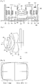
- FIG. 1 is a diagram showing a camera module according to the embodiment.
- FIG. 2 is a diagram illustrating an optical system including a lens assembly, an IR cut-off filter unit, and a sensor unit.
- FIG. 3 is a diagram illustrating an image incident onto the sensor unit through the lens assembly.
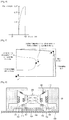
- FIG. 4 is a diagram illustrating distortion in an optical system including a lens assembly, an IR cut-off filter unit, and a sensor unit.
- FIG. 5 is a diagram illustrating movement of an image due to hand-shaking and compensation thereof.
- the camera module includes a lens barrel 100, a lens assembly 200, a first elastic member 310, a second elastic member 320, a first housing 410, a second housing 420, an IR cut-off filter unit 500 and a sensor unit 600, a circuit board 800, and driving units 710, 720, 730, and 740.
- the lens barrel 100 receives the lens assembly 200 therein.
- the lens barrel 100 has a receiving groove for receiving the lens assembly 200.
- the receiving groove may have a shape corresponding to a shape of the lens assembly 200.
- the lens barrel 100 may have a rectangular shape or a cylindrical shape. That is, the outer portion of the lens barrel 100 may have a rectangular shape or a circular shape.
- the lens barrel 100 may be connected with the first housing 410.
- the lens barrel 100 is connected to the first housing 410 through the first elastic member 310. That is, the lens barrel 100 may be movably connected to the first housing 410 by the first elastic member 310.
- the lens barrel 100 includes a light incident groove, which is open upward (toward an object).
- the light incident groove exposes the lens assembly 200.
- An image is incident into the lens assembly 200 through the light incident groove.
- the lens assembly 200 is disposed in the lens barrel 100.
- the lens assembly 200 is disposed in the receiving groove.
- the lens assembly 200 is inserted into the receiving groove.
- the outer portion of the lens assembly 200 may have a circular shape.
- the outer portion of the lens assembly 200 may have a circular shape when viewed from the top.
- the lens assembly 200 may have a rectangular shape when viewed from the top.
- the lens assembly 200 includes a plurality of lenses 210, 220, 230, and 240.
- the lens assembly 200 may include a first lens 210, a second lens 220, a third lens 230 and a fourth lens 240.
- the third lens 230, the second lens 220, and the first lens 210 may be sequentially laminated.
- a first spacer and a second spacer may be interposed among the lenses 210, 220, 230, and 240.
- the lenses 210, 220, 230, and 240 are spaced apart from each other through the first spacer and the second spacer.
- the lens assembly 200 includes four lenses, the embodiment is not limited thereto. That is, the lens assembly 200 may include one to three lenses or at least five lenses.
- the lens assembly 200, the IR cut-off filter unit 500, and the sensor unit 600 constitute the optical system.
- the first lens 210, the second lens 220, the third lens 230, and the fourth lens 240 may be sequentially disposed from the object side to the image side.
- light corresponding to image information of the subject is incident to the sensor unit 600 by passing through the first lens 210, the second lens 220, the third lens 230, the fourth lens 240, and the IR cut-off filter unit 500.
- the first lens 210 may have positive (+) refractive power
- the second lens 220 may have negative (-) refractive power
- the third lens 230 may have the positive (+) refractive power
- the fourth lens 240 may have the negative (-) refractive power.
- the first lens 210, the second lens 220, the third lens 230, and the fourth lens 240 may include glass or plastic.
- the first lens 210 has a convex surface at the object side R1 thereof, and the first lens 210 has a convex, concave, flat surface at the image side R2 thereof. Further, the first lens 210 may have an aspherical or spherical surface at the object side R1 thereof. Preferably, the first lens 210 has double-convex surfaces in the vicinity of an optical axis.
- a curvature of the image side R2 of the first lens 210 may satisfy the following equation 1. 0 ⁇ R ⁇ 0.01
- the curvature of the image side R2 of the first lens 210 may satisfy the following equation 7. 0 ⁇ R ⁇ 0.001
- the curvature of the image side R2 of the first lens 210 may be zero (0). That is, the image side R2 of the first lens 210 may have a very small curvature.
- the image side R2 of the first lens 210 may include the flat surface.
- the image side R2 of the first lens 210 may have the flat surface or a curved surface similar to the flat surface.
- the image side R2 of the first lens 210 is similar to the flat surface so that tolerance of a small optical system according to the embodiment may be reduced.
- the second lens 220 may have a meniscus shape.
- the second lens 220 may have a concave surface at the object side R1 thereof and the second lens 220 may have a concave surface at the image side R4 thereof. That is, the second lens 220 may have double-concave shapes.
- the second lens 220 may have a spherical or aspherical surface at the object side R3 and the image side R4 thereof. It is preferable that the second lens 220 has a meniscus shape where a concave surface is directed to the object side.
- the third lens 230 has a convex surface at the image side thereof in the vicinity of the optical axis and has positive power.
- the third lens 230 may have a concave surface at the object side thereof in the vicinity of the optical axis.
- the third lens 230 may have a concave surface at the object side thereof and have a convex surface at the image side R6 thereof.
- the third lens 230 may have a spherical or aspherical surface at the object side R5 and the image side R6 thereof.
- the focus length of the third lens 230 may satisfy the following equation 2. 0.5 ⁇ f 3 / F ⁇ 1.0
- Equation 2 f3 represents an effective focal distance of the third lens 230, and F represents a whole focus distance of a small optical system according to the embodiment.
- the focus length of the third lens 230 may satisfy the following equation 4. 0.6 ⁇ f 3 / F ⁇ 0.9
- the fourth lens 240 may have a meniscus shape.
- the fourth lens 240 may have a convex surface at an object side R7 thereof and the fourth lens 240 may have a concave surface at an image side R8 thereof.
- the fourth lens 240 may have an aspherical surface at the object side R7 and the image side R8 thereof.
- the fourth lens 240 includes at least one aspheric inflection point.
- the at least one aspheric inflection point may be formed on the object side R7 of the fourth lens 240.
- the at least one aspheric inflection point CP may be formed on the image side R8 of the fourth lens 240.
- the aspheric inflection point of the fourth lens 240 may adjust the maximum radiation angle of a main light incident into the light receiving device 70.
- the focus length of the fourth lens 240 may satisfy the following equation 3. ⁇ 10 ⁇ f 4 / F ⁇ ⁇ 0.5
- Equation 3 f4 represents an effective focal distance of the fourth lens 240, and F represents a whole focus distance of a small optical system according to the embodiment.
- the focus length of the third lens 230 may satisfy the following equation 5. ⁇ 1 ⁇ f 4 / F ⁇ ⁇ 0.5
- the light receiving device 70 serving as an imaging surface R14 is a charge coupled device (CCD) or a complementary metal oxide semiconductor (CMOS), an angle to ensure the quantity of light exists with respect to each pixel. If a different angle is used in the pixel, the quantity of light is not ensured, a shading phenomenon in which an outer portion of the image is darkened.
- CCD charge coupled device
- CMOS complementary metal oxide semiconductor
- the maximum of incident angle of the main ray is adjusted by forming the aspheric inflection point at the image side R8 of the fourth lens 240 facing the image side, thereby preventing the outer portion of the image screen from being darkened.
- the small optical system may satisfy the following Equation 6. 1 ⁇ ttl / F ⁇ 1.3
- Equation 6 tt1 represents a distance between the object side of the first lens 210 and the image side thereof, and F represents the whole effective focus length.
- the optical system of the embodiment may have a negative distortion. That is, as shown in FIGS. 3 and 4 , the optical system may the negative distortion.
- a distortion of an image of the sensor unit 600 may be in the range of -2 % to 0 %.
- the distortion of an image of the sensor unit 600 may be in the range of 0 % to -2 %.
- the distortion of an image of the sensor unit 600 may be in the range of -2 % to -5 %.
- the distortion of an image of the sensor unit 600 may be in the range of -2 % to -5 %.
- the first elastic member 310 is disposed in the first housing 410.
- the first elastic member 310 is fixed to the first housing 410. Further, the first elastic member 310 is fixed to the lens barrel 100.
- the first elastic member 310 movably fixes the lens barrel 100 to the first housing 410.
- the first elastic member 310 may include a spring.
- the first elastic member 310 may include a leaf spring.
- the first housing 410 receives the lens barrel 100.
- the first housing 410 is connected to the lens barrel 100 through the first elastic member 310.
- the first housing 410 may include plastic or metal.
- the first housing 410 may have a rectangular container shape.
- the second housing 420 receives the first housing 410. That is, the first housing 410 is disposed in the second housing 420. The first housing 410 is connected to the second housing 420 by the second elastic member 320.
- the first housing 410 is movably fixed in the second housing 420 by the second elastic member 320.
- the first housing 410 may float in the second housing 420.
- the second housing 420 is fixed to the circuit board 800.
- the second housing 420 may be coupled with the circuit board 800.
- the second housing 420 may include plastic or metal.
- the second elastic member 320 is connected to the first housing 410 and the second housing 420.
- the second elastic member 320 movably fixes the first housing 410 to the second housing 420.
- the second elastic member 320 may include a spring.
- the second elastic member 320 may include a leaf spring.
- the IR cut-off filter unit 500 is disposed in the second housing 420.
- the IR cut-off filter unit 500 is fixed to the circuit board 800 and may be fixed to the second housing 420.
- the IR cut-off filter unit 500 filters an incident IR.
- the IR cut-off filter unit 500 may filter light having an excessively long wavelength introduced into the sensor unit 600.
- the IR cut-off filter unit 500 may be formed by alternately depositing titanium oxide and silicon oxide on optical glass. In order to cut-off the IR, thicknesses of the titanium oxide and the silicon oxide may be suitable adjusted.
- the sensor unit 600 is received in the second housing 420.
- the sensor unit 600 includes a CCD image sensor and a CMOS image sensor.
- the sensor unit 600 further includes the circuit board 800 connected to the image sensor.
- the sensor unit 600 converts an incident image into an electrical signal.
- the sensor unit 600 is fixed to the circuit board 800.
- the sensor unit 600 may be mounted on the circuit board 800.
- the sensor unit 600 is electrically connected to the circuit board 800.
- a photographing region of the sensor unit 600 may have the size of 2.5 mm ⁇ 4.0 mm. Further, a unit cell of the sensor unit 600 may have length and breadth of 2 ⁇ m or less.
- the circuit board 800 may cover a bottom of the second housing 420. The circuit board 800 is coupled with the second housing 420.
- the circuit board 800 may include a printed circuit board (PCB).
- the circuit board 800 may be electrically connected to the sensor unit 600.
- the circuit board 800 may apply a signal for driving the sensor unit 600. Further, the circuit board 800 may receive a signal from the sensor unit 600.
- the sensor unit 600 is mounted on the circuit board 800.
- the sensor unit 600 may be fixed to the circuit board 800. That is, the sensor unit 600 may be fixed to the second housing 420 through the circuit board 800.
- the circuit board 800 may be electrically connected to the driving units 710, 720, 730, and 740. That is, a signal for driving the driving units 710, 720, 730, and 740 may be applied to the driving units 710, 720, 730, and 740 through the circuit board 800.
- the driving units 710, 720, 730, and 740 drive the lens barrel 100 with respect to the first housing 410.
- the driving units 710, 720, 730, and 740 drive the first housing 410 with respect to the second housing 420.
- the driving units 710, 720, 730, and 740 may move the lens barrel 100 and the first housing 410 by a magnetic force.
- the driving units 710, 720, 730, and 740 may include a first driving unit 710, a second driving unit 720, a third driving unit 730, and a fourth driving unit 740.
- the driving units 710, 720, 730, and 740 may move the lens barrel relative to the housing 400 by a magnetic force. In this case, the magnetic force may be applied to a direction inclined with respect to the optical axis OA of the lens assembly 200.
- the first driving unit 710 is attached to the lens barrel 100.
- the first driving unit 710 may be fixed to the lens barrel 100.
- the first driving unit 710 may be disposed at an outer side of the lens barrel 100.
- the first driving unit 710 may include a coil.
- the first driving unit 710 may receive a driving signal through the circuit board 800.
- the first driving unit 710 may generate a magnetic field according to an electrical signal.
- the first driving unit 710 may apply an attractive force or a repulsive force to the second driving unit 720 in a direction inclined with respect to a reference horizontal plane.
- the first driving unit 710 may apply the magnetic force to the second driving unit 720 at an angle of about +20° to about +70° with respect to the reference horizontal plane.
- the first driving unit 710 may apply the magnetic force to the second driving unit 720 at an angle of about +30° to about +50° with respect to the reference horizontal plane R.
- the second driving unit 720 is attached to the first housing 410.
- the second driving unit 720 may be fixed to the first housing 410.
- the second driving unit 720 may be fixed to an inner side of the first housing 410.
- the second driving unit 720 includes a magnetic material.
- the second driving unit 720 may have a plate shape. That is, the second driving unit 720 may be prepared as a plate magnet.
- the first driving unit 710 is close to the second driving unit 720.
- the first driving unit 710 may be spaced apart from the second driving unit 720 by a very small distance.
- the distance between the first driving unit 710 and the second driving unit 720 may be in the range of about 50 ⁇ m to about 1000 ⁇ m.
- the first driving unit 710 may face the second driving unit 720. Accordingly, a magnetic field may be generated between the first driving unit 710 and the second driving unit 720.
- the first driving unit 710 and the second driving unit 720 move the lens barrel 100 relative to the first housing 410.
- the first driving 710 and the second driving unit 720 may move the lens barrel 100 relative to the first housing 410 in an optical-axis direction of the lens assembly 200.
- the third driving unit 730 is attached to the first housing 410.
- the third driving unit 730 may be fixed to the first housing 410.
- the third driving unit 730 may be fixed to an outer side of the first housing 410.
- the third driving unit 730 includes a magnetic material.
- the third driving unit 730 may have a plate shape. That is, the third driving unit 730 may be prepared as a plate magnet.
- the fourth driving unit 740 is attached to the second housing 420. In detail, the fourth driving unit 740 may be fixed to the second housing 420. In more detail, the fourth driving unit 740 may be fixed to an inner side of the second housing 420.
- the fourth driving unit 740 may include a coil.
- the fourth driving unit 740 may receive a driving signal through the circuit board 800.
- the fourth driving unit 740 may generates a magnetic field according to an electrical signal.
- the third driving unit 730 is close to the fourth driving unit 740.
- the third driving unit 730 may be spaced apart from the fourth driving unit 740 by a very small distance.
- the distance between the third driving unit 730 and the fourth driving unit 740 may be in the range of about 50 ⁇ m to about 1000 ⁇ m.
- the third driving unit 730 may face the fourth driving unit 740. Accordingly, a magnetic force may be generated between the third driving unit 730 and the fourth driving unit 740.
- the third driving unit 730 and the fourth driving unit 740 move the first housing 410 relative to the second housing 420.
- the third driving 730 and the fourth driving unit 740 may move the first housing 410 relative to the second housing 420 in a horizontal direction with respect to an optical axis of the lens assembly 200.
- the driving units 710, 720, 730, and 740 may move the lens assembly 200 relative to the sensor unit 600 in the optical axis direction and in a direction horizontal to the optical axis.
- the first housing 410 may be tilted or horizontally moved by the third driving unit 730 and the fourth driving unit 740. Accordingly, a relative horizontal location between the lens assembly 200 and the sensor 600 may be adjusted.
- a focus length between the lens assembly 200 and the sensor unit 600 may be adjusted by the first driving unit 710 and the second driving unit 720.
- the optical system since the optical system has a negative distortion, movement of an image according to shaking in a horizontal direction is minimized, and accordingly, a compensation error may be reduced.
- the driving units 710, 720, 730, and 740 move the lens barrel 100 in a direction opposite to a moving direction of the image.
- the driving units 710, 720, 730, and 740 move the image to the initial position by horizontally moving or tilting the lens barrel 100.
- an error of an image according to movement of the lens barrel 100 may be minimized in an outer peripheral portion of the image.
- the optical system of the camera module according to the embodiment has the negative distortion, so it is possible to prevent the movement distance of the image from being increased due to the shaking as the image is located away from the optical axis.
- the camera module according to the embodiment can minimize image shaking at an outer peripheral portion of the photographing region and maximize a shaking correction effect.
- FIG. 6 is a diagram showing a camera module according to another embodiment. The embodiment will be described by making reference to the above description of the camera module. The description of the previous embodiment with respect to the camera module may be incorporated in the description of the embodiment except for the modifications.
- the first housing 410 may be omitted from the camera module according to the embodiment.
- a second housing 420 may be directly connected to the lens barrel 100 through an elastic member.
- the elastic member may connect the lens barrel 110 to the second housing 420 in a direction inclined with respect to an optical axis of the lens assembly 200.
- the first driving unit 710 is attached to the lens barrel 110.
- the first driving unit 710 may include a magnetic material.
- a fourth driving unit 740 is attached to an inner side of the second housing 420.
- the fourth driving unit 740 may include a coil.
- a fifth driving unit 750 is attached onto the circuit board 800.
- the fifth driving unit 750 may be interposed between the first driving unit 710 and the circuit board 800.
- the fifth driving unit 750 may include a coil.
- fourth driving unit 740 and the fifth driving unit 750 may be electrically to the circuit board 800.
- the lens barrel 100 may be driven in a horizontal direction perpendicular to the optical axis by a magnetic force between the first driving unit 710 and the fourth driving unit 740. Moreover, the lens barrel 100 may be driven in the optical axis direction by a magnetic force between the first driving unit 710 and the fifth driving unit 750.
- the lens barrel 100 may be driven in the horizontal direction by the first driving unit 710 and the fourth driving unit 740. Further, the lens barrel 100 may be driven in the optical axis direction by the first driving unit 710 and the fifth driving unit 750.
- the camera module according to the embodiment may correct shaking and adjust automatic focus by a simple structure.
- FIG. 7 is a diagram showing a camera module according to another embodiment. The embodiment will be described by making reference to the above description of the camera module. The description of the previous embodiment with respect to the camera module may be incorporated in the description of the embodiment except for the modifications.
- a third driving unit 730 is omitted and a fourth driving unit 740 may be close to the second driving unit 720.
- the fourth driving unit 740 may be interposed between the second driving unit 720 and the circuit board 800.
- the first housing 410 may be relatively moved according to an attractive force or a repulsive force between the second driving unit 720 and the fourth driving unit 740.
- the lens barrel 100 may be driven according to the attractive force or the repulsive force between the first driving unit 710 and the second driving unit 720, and the first housing 410 may be driven according to a magnetic force between the second driving unit 720 and the fourth driving unit 740. That is, the first driving unit 710 may share the second driving unit 720 with the fourth driving unit 740
- the camera module according to the embodiment may have reduced number of components and have the simple structure by omitting the third driving unit 730.
Landscapes
- Physics & Mathematics (AREA)
- General Physics & Mathematics (AREA)
- Optics & Photonics (AREA)
- Engineering & Computer Science (AREA)
- Multimedia (AREA)
- Signal Processing (AREA)
- Studio Devices (AREA)
- Lens Barrels (AREA)
- Adjustment Of Camera Lenses (AREA)
- Lenses (AREA)
- Camera Bodies And Camera Details Or Accessories (AREA)
Claims (14)
- Linsenantriebsvorrichtung zum Antreiben einer Linsenanordnung, wobei die Linsenantriebsvorrichtung umfasst:ein Gehäuse, das ein erstes Gehäuse (410) und ein zweites Gehäuse (420) umfasst, wobei das zweite Gehäuse (420) einen Abschnitt umfasst, der unter dem ersten Gehäuse (410) angeordnet ist, wobei das erste Gehäuse (410) einen Seitenabschnitt und einen oberen Abschnitt umfasst, der sich in horizontaler Richtung von einem Ende des Seitenabschnitts erstreckt;einen Zylinder (100), der in dem ersten Gehäuse (410) angeordnet ist und dazu konfiguriert ist, die Linsenanordnung aufzunehmen;ein erstes elastisches Element (310), das den Zylinder (100) und den oberen Abschnitt des ersten Gehäuses (410) derart verbindet, dass sich der Zylinder (100) bezogen auf das erste Gehäuse (410) in einer vertikalen Richtung bewegt;ein zweites elastisches Element (320) zum beweglichen Fixieren des ersten Gehäuses (410) an dem zweiten Gehäuse (420);eine erste Spule (710), die an einer Außenseite des Zylinders (100) befestigt ist,einen Magneten (720), der an einer Innenoberfläche des Seitenabschnitts des ersten Gehäuses (410) angeordnet ist und mit der ersten Spule (710) zusammenwirkt, um den Zylinder (100) und die erste Spule (710) bezüglich des ersten Gehäuses (410) in vertikaler Richtung zu bewegen; undeine zweite Spule (740), die an dem zweiten Gehäuse (420) angeordnet ist und mit dem Magneten (720) zusammenwirkt, um das erste Gehäuse (410) und den Magneten (720) derart zu bewegen, dass sich der Zylinder (100) bezüglich des zweiten Gehäuses (420) in horizontaler Richtung bewegt;wobei der Magnet (720) eine untere Oberfläche, eine obere Oberfläche und Seitenoberflächen umfasst;wobei die Seitenoberflächen des Magneten (720) eine erste Seitenoberfläche, die der ersten Spule (710) zugewandt ist, und eine zweite Seitenoberfläche, die der ersten Seitenoberfläche gegenüberliegt, umfasst, wobei die zweite Seitenoberfläche des Magneten (720) an der Innenoberfläche des Seitenabschnitts des ersten Gehäuses (410) angeordnet ist;dadurch gekennzeichnet, dass die erste Spule (710) der ersten Seitenoberfläche des Magneten (720) in horizontaler Richtung zugewandt ist und die zweite Spule (740) der unteren Oberfläche des Magneten (720) in vertikaler Richtung zugewandt ist, so dass die erste Spule (710) und die zweite Spule (740) mit dem Magneten (720) zusammenwirken; undwobei die zweite Spule (740) zwischen der unteren Oberfläche des Magneten (720) und einer oberen Oberfläche des zweiten Gehäuses (420) in vertikaler Richtung angeordnet ist,wobei in vertikaler Richtung eine Breite der ersten Seitenoberfläche des Magneten größer ist als eine Breite der ersten Spule, die der ersten Seitenoberfläche des Magneten zugewandt ist,wobei in horizontaler Richtung eine Breite zwischen der ersten Seitenoberfläche des Magneten und der zweiten Seitenoberfläche des Magneten kleiner ist als eine Breite der zweiten Spule, die der unteren Oberfläche des Magneten zugewandt ist,wobei die zweite Spule (740) einen Mittelabschnitt, der die untere Oberfläche des Magneten in vertikaler Richtung überlappt, und einen Außenabschnitt umfasst, der sich horizontal von dem Mittelabschnitt in eine dem Zylinder entgegengesetzte Richtung erstreckt, undwobei der Außenabschnitt der zweiten Spule einer Bodenoberfläche des Seitenabschnitts des ersten Gehäuses zugewandt ist.
- Linsenantriebsvorrichtung nach Anspruch 1,
wobei der Außenabschnitt der zweiten Spule zwischen dem Seitenabschnitt des ersten Gehäuses und des zweiten Gehäuses in vertikaler Richtung angeordnet ist. - Linsenantriebsvorrichtung nach Anspruch 1 oder 2, wobei der Magnet (720) die Form einer Platte hat,
wobei die erste Spule (710) an der Außenseite des Zylinders (100) fixiert ist, und
wobei ein Bereich der ersten Spule, der der ersten Seitenoberfläche des Magneten (720) zugewandt ist, dazu konfiguriert ist, zwischen der oberen Oberfläche des Magneten und der unteren Oberfläche des Magneten, in horizontaler Richtung gesehen, positioniert zu werden. - Linsenantriebsvorrichtung nach einem der Ansprüche 1 bis 3, wobei die zweite Spule (740) einen inneren Abschnitt umfasst, der bezüglich des Mittelabschnitts innen angeordnet ist, und
wobei die zweite Spule (740) niedriger als die Bodenoberfläche des Zylinders (100) angeordnet ist. - Linsenantriebsvorrichtung nach einem der Ansprüche 1 bis 4, wobei in einer Ausgangsposition des Zylinders die erste Spule näher an der unteren Oberfläche des Magneten positioniert ist als an der oberen Oberfläche des Magneten.
- Linsenantriebsvorrichtung nach einem der Ansprüche 1 bis 5,
wobei wenigstens ein Abschnitt der zweiten Spule dem ersten Gehäuse zugewandt ist und mit dem ersten Gehäuse in vertikaler Richtung überlappt ist. - Linsenantriebsvorrichtung nach einem der Ansprüche 1 bis 6, wobei die erste Spule (710) und der Magnet (720) dazu konfiguriert sind, eine Fokussierungsfunktion derart durchzuführen, dass sich der Zylinder (100) und die erste Spule (710) bei Betrieb der Autofokusfunktion relativ zum oberen Abschnitt des ersten Gehäuses (410) in vertikaler Richtung bewegen, und
wobei der Magnet (720) und die zweite Spule (740) dazu konfiguriert sind, eine Rüttelkompensationsfunktion derart durchzuführen, dass sich das erste Gehäuse (410) und der Magnet (720) bei Betrieb der Rüttelkompensationsfunktion relativ zu dem zweiten Gehäuse (420) in der horizontalen Richtung bewegen. - Linsenantriebsvorrichtung nach einem der Ansprüche 1 bis 7, wobei das zweite Gehäuse (420) eine Öffnung umfasst, die unter dem Zylinder (100) derart angeordnet ist, dass Licht von einem Gegenstand durch den Zylinder (100) und durch die Öffnung des zweiten Gehäuses (420) hindurchtritt.
- Linsenantriebsvorrichtung nach einem der Ansprüche 1 bis 8, wobei die zweite Seitenfläche des Magneten (720) an der Innenoberfläche des Seitenabschnitts des ersten Gehäuses (410) fixiert ist, und
wobei die Innenoberfläche des Seitenabschnitts des ersten Gehäuses (410) mit der zweiten Seitenoberfläche des Magneten (720) in horizontaler Richtung überlappt ist. - Linsenantriebsvorrichtung nach einem derAnsprüche 1 bis 9, wobei der Magnet (720) und die erste Spule (710) unterhalb des oberen Abschnitts des ersten Gehäuses (410) angeordnet sind.
- Linsenantriebsvorrichtung nach einem der Ansprüche 1 bis 10, wobei die erste Spule (710) von dem Magneten (720) mit einem Abstand in einem Bereich von 50 µm bis 1000 µm in horizontaler Richtung beabstandet ist.
- Linsenantriebsvorrichtung nach einem derAnsprüche 1 bis 11, wobei die zweite Spule (740) von dem Magneten (720) mit einen Abstand in einem Bereich von 50 µm bis 1000 µm in vertikaler Richtung beabstandet ist.
- Kameramodul, umfassend:die Linsenantriebsvorrichtung nach einem der Ansprüche 1 bis 12;die Linsenanordnung (200), die in dem Zylinder der Linsenantriebsvorrichtung angeordnet ist;einen Bildsensor (600), der unter dem zweiten Gehäuse (420) der Linsenantriebsvorrichtung angeordnet ist; undeine Leiterplatte (800), auf der der Bildsensor (600) montiert ist, wobei der Bildsensor (600) elektrisch mit der Leiterplatte (800) verbunden ist,wobei die erste Spule (710) und die zweite Spule (740) der Linsenantriebsvorrichtung jeweils konfiguriert ist, um ein Antriebssignal von der Leiterplatte (800) zu empfangen, undwobei die Leiterplatte (800) unter dem zweiten Gehäuse (420) der Linsenantriebsvorrichtung angeordnet ist.
- Kameramodul nach Anspruch 13, wobei die Linsenanordnung vier Linsen umfasst,
wobei ein Abstand zwischen der zweiten Spule und dem Bildsensor bei Betrieb einer Rüttelkompensationsfunktion konstant bleibt, und
wobei eine Einheitszelle des Bildsensors eine Länge von 2 µm oder weniger oder eine Breite von 2 µm oder weniger aufweist.
Priority Applications (2)
| Application Number | Priority Date | Filing Date | Title |
|---|---|---|---|
| EP20198136.2A EP3790268B1 (de) | 2012-06-29 | 2013-06-28 | Kameramodul |
| EP23190989.6A EP4277292A3 (de) | 2012-06-29 | 2013-06-28 | Kameramodul |
Applications Claiming Priority (4)
| Application Number | Priority Date | Filing Date | Title |
|---|---|---|---|
| KR1020120071201A KR101500034B1 (ko) | 2012-06-29 | 2012-06-29 | 카메라 모듈 |
| EP16183075.7A EP3119076B1 (de) | 2012-06-29 | 2013-06-28 | Kameramodul |
| PCT/KR2013/005777 WO2014003493A1 (en) | 2012-06-29 | 2013-06-28 | Camera module |
| EP13810457.5A EP2868076B1 (de) | 2012-06-29 | 2013-06-28 | Kameramodul |
Related Parent Applications (3)
| Application Number | Title | Priority Date | Filing Date |
|---|---|---|---|
| EP16183075.7A Division EP3119076B1 (de) | 2012-06-29 | 2013-06-28 | Kameramodul |
| EP16183075.7A Division-Into EP3119076B1 (de) | 2012-06-29 | 2013-06-28 | Kameramodul |
| EP13810457.5A Division EP2868076B1 (de) | 2012-06-29 | 2013-06-28 | Kameramodul |
Related Child Applications (3)
| Application Number | Title | Priority Date | Filing Date |
|---|---|---|---|
| EP20198136.2A Division EP3790268B1 (de) | 2012-06-29 | 2013-06-28 | Kameramodul |
| EP20198136.2A Division-Into EP3790268B1 (de) | 2012-06-29 | 2013-06-28 | Kameramodul |
| EP23190989.6A Division EP4277292A3 (de) | 2012-06-29 | 2013-06-28 | Kameramodul |
Publications (2)
| Publication Number | Publication Date |
|---|---|
| EP3496385A1 EP3496385A1 (de) | 2019-06-12 |
| EP3496385B1 true EP3496385B1 (de) | 2020-11-11 |
Family
ID=49783542
Family Applications (5)
| Application Number | Title | Priority Date | Filing Date |
|---|---|---|---|
| EP13810457.5A Active EP2868076B1 (de) | 2012-06-29 | 2013-06-28 | Kameramodul |
| EP23190989.6A Pending EP4277292A3 (de) | 2012-06-29 | 2013-06-28 | Kameramodul |
| EP19150652.6A Active EP3496385B1 (de) | 2012-06-29 | 2013-06-28 | Linsenantriebsvorrichtung |
| EP16183075.7A Active EP3119076B1 (de) | 2012-06-29 | 2013-06-28 | Kameramodul |
| EP20198136.2A Active EP3790268B1 (de) | 2012-06-29 | 2013-06-28 | Kameramodul |
Family Applications Before (2)
| Application Number | Title | Priority Date | Filing Date |
|---|---|---|---|
| EP13810457.5A Active EP2868076B1 (de) | 2012-06-29 | 2013-06-28 | Kameramodul |
| EP23190989.6A Pending EP4277292A3 (de) | 2012-06-29 | 2013-06-28 | Kameramodul |
Family Applications After (2)
| Application Number | Title | Priority Date | Filing Date |
|---|---|---|---|
| EP16183075.7A Active EP3119076B1 (de) | 2012-06-29 | 2013-06-28 | Kameramodul |
| EP20198136.2A Active EP3790268B1 (de) | 2012-06-29 | 2013-06-28 | Kameramodul |
Country Status (6)
| Country | Link |
|---|---|
| US (7) | US9860432B2 (de) |
| EP (5) | EP2868076B1 (de) |
| JP (6) | JP6352254B2 (de) |
| KR (1) | KR101500034B1 (de) |
| CN (4) | CN108196413B (de) |
| WO (1) | WO2014003493A1 (de) |
Families Citing this family (48)
| Publication number | Priority date | Publication date | Assignee | Title |
|---|---|---|---|---|
| US8982464B2 (en) * | 2010-10-22 | 2015-03-17 | Tdk Taiwan Corporation | Tilt-type anti-shake compensation structure for auto-focus module |
| KR101500034B1 (ko) | 2012-06-29 | 2015-03-06 | 엘지이노텍 주식회사 | 카메라 모듈 |
| TWI548926B (zh) * | 2013-05-06 | 2016-09-11 | 台灣東電化股份有限公司 | 具3軸閉路回饋控制模組之電磁驅動鏡頭裝置 |
| CN114679528B (zh) | 2014-01-03 | 2024-04-30 | Lg伊诺特有限公司 | 音圈马达和摄像头模块 |
| WO2015147603A1 (ko) * | 2014-03-27 | 2015-10-01 | 주식회사 디원 | 흔들림 보정 기능을 갖는 카메라모듈 |
| JP2016051078A (ja) | 2014-08-29 | 2016-04-11 | 日本電産コパル株式会社 | レンズ駆動装置 |
| US10502924B2 (en) | 2015-07-10 | 2019-12-10 | Lg Innotek Co., Ltd. | Lens driving device, camera module, and optical device |
| KR102388119B1 (ko) * | 2015-08-18 | 2022-04-20 | 엘지이노텍 주식회사 | 카메라 장치 및 광학기기 |
| CN107040118B (zh) * | 2016-02-04 | 2020-06-05 | 台湾东电化股份有限公司 | 电磁驱动模块及应用该电磁驱动模块的镜头驱动装置 |
| KR102052791B1 (ko) * | 2016-05-18 | 2019-12-06 | 삼성전기주식회사 | 카메라 모듈 |
| CN109154711B (zh) * | 2016-06-30 | 2021-03-09 | Lg 电子株式会社 | 相机模块和及其自动对焦的方法 |
| JP2018018055A (ja) * | 2016-07-13 | 2018-02-01 | オリンパス株式会社 | 像振れ補正装置 |
| TWI650587B (zh) * | 2016-08-04 | 2019-02-11 | 台灣東電化股份有限公司 | 鏡頭驅動裝置 |
| WO2018044083A1 (ko) | 2016-09-02 | 2018-03-08 | 엘지이노텍 주식회사 | 광출력 모듈 및 라이다 |
| KR102817313B1 (ko) * | 2016-09-02 | 2025-06-09 | 엘지이노텍 주식회사 | 광출력 모듈 및 라이다 |
| KR102761114B1 (ko) * | 2016-09-13 | 2025-02-04 | 엘지이노텍 주식회사 | 광출력 모듈 및 라이다 |
| CN107995386B (zh) * | 2016-10-26 | 2021-01-26 | 光宝电子(广州)有限公司 | 相机模块 |
| TWI615651B (zh) * | 2016-12-07 | 2018-02-21 | 台灣東電化股份有限公司 | 自動對焦及光學防手震機構之整合結構 |
| KR102690766B1 (ko) * | 2017-02-22 | 2024-08-01 | 엘지전자 주식회사 | 카메라 모듈 및 그 제어 방법 |
| DE102017003231A1 (de) * | 2017-04-03 | 2018-10-04 | Mühlbauer Gmbh & Co. Kg | Optisches Bauteilerfassungssystem und Verfahren zum Erfassen mindestens eines Bauteils |
| KR102402616B1 (ko) * | 2017-05-26 | 2022-05-27 | 엘지이노텍 주식회사 | 렌즈 구동 장치, 및 이를 포함하는 카메라 모듈 및 광학 기기 |
| KR102435025B1 (ko) | 2017-09-25 | 2022-08-23 | 삼성전자주식회사 | 다른 자기장의 방향을 갖는 복수의 구동부를 포함하는 카메라 모듈 |
| JP6846533B2 (ja) * | 2017-09-27 | 2021-03-24 | 富士フイルム株式会社 | 像ぶれ補正装置及び撮像装置 |
| TWI652540B (zh) | 2018-01-05 | 2019-03-01 | 緯創資通股份有限公司 | X光機、電子裝置及x光機的操作方法 |
| CN209375770U (zh) * | 2018-01-25 | 2019-09-10 | 台湾东电化股份有限公司 | 光学系统 |
| EP3798724B1 (de) | 2018-05-23 | 2023-11-08 | LG Innotek Co., Ltd. | Linsenansteuerungsvorrichtung und kameramodul sowie optische vorrichtung damit |
| CN209446872U (zh) * | 2018-05-30 | 2019-09-27 | 台湾东电化股份有限公司 | 光学元件驱动机构 |
| JP7064819B2 (ja) * | 2019-06-01 | 2022-05-11 | エーエーシー オプティックス ソリューションズ ピーティーイー リミテッド | レンズモジュール |
| WO2021115604A1 (en) * | 2019-12-12 | 2021-06-17 | Huawei Technologies Co., Ltd. | Voice coil actuator with multistep movement |
| CN115053176A (zh) * | 2020-01-30 | 2022-09-13 | 日本电产株式会社 | 带抖动校正功能的光学单元 |
| CN113630528A (zh) * | 2020-05-08 | 2021-11-09 | 南昌欧菲光电技术有限公司 | 防抖组件、摄像模组及电子设备 |
| KR102883045B1 (ko) * | 2020-05-29 | 2025-11-07 | 엘지이노텍 주식회사 | 카메라 엑추에이터 및 이를 포함하는 카메라 장치 |
| TWI731724B (zh) * | 2020-06-20 | 2021-06-21 | 大陽科技股份有限公司 | 攝影鏡頭、鏡頭驅動模組與電子裝置 |
| US11172131B1 (en) | 2020-06-29 | 2021-11-09 | Western Digital Technologies, Inc. | Optical devices for tilt in camera systems |
| US11277566B2 (en) | 2020-06-29 | 2022-03-15 | Western Digital Technologies, Inc. | Optical devices for independent movement control of lenses and image sensors in camera systems |
| US11277565B2 (en) * | 2020-06-29 | 2022-03-15 | Western Digital Technologies, Inc. | Optical devices for independent movement control of lenses and image sensors in camera systems |
| US11212447B1 (en) | 2020-06-29 | 2021-12-28 | Western Digital Technologies, Inc. | Optical devices for tilt in camera systems |
| KR20220040310A (ko) * | 2020-09-23 | 2022-03-30 | 삼성전자주식회사 | 카메라 모듈 및 이를 포함하는 전자 장치 |
| CN113296226B (zh) * | 2021-06-09 | 2024-11-08 | 中山联合光电科技股份有限公司 | 变焦镜头及摄影设备 |
| KR102846697B1 (ko) * | 2021-07-09 | 2025-08-14 | 엘지이노텍 주식회사 | 카메라 모듈 |
| KR20230025991A (ko) * | 2021-08-17 | 2023-02-24 | 엘지이노텍 주식회사 | 센서 구동 장치 및 이를 포함하는 카메라 모듈 |
| TWI787986B (zh) * | 2021-09-01 | 2022-12-21 | 海華科技股份有限公司 | 可攜式電子裝置及其影像擷取模組 |
| CN115061325A (zh) * | 2021-09-08 | 2022-09-16 | 新思考电机有限公司 | 透镜驱动装置、照相机装置以及电子设备 |
| CN116490822B (zh) | 2021-11-17 | 2026-04-10 | 三星电子株式会社 | 相机模块和包括该相机模块的电子装置 |
| CN116437208B (zh) * | 2021-12-31 | 2025-08-22 | 华为技术有限公司 | 一种驱动装置、防抖成像装置和终端 |
| CN115047581A (zh) * | 2022-05-23 | 2022-09-13 | 高瞻创新科技有限公司 | 一种微型防抖云台相机模组 |
| KR102946073B1 (ko) * | 2023-03-23 | 2026-04-01 | 삼성전기주식회사 | 카메라 모듈 |
| WO2025244426A1 (ko) * | 2024-05-22 | 2025-11-27 | 삼성전자 주식회사 | 카메라 모듈 및 이를 포함하는 전자 장치 |
Family Cites Families (65)
| Publication number | Priority date | Publication date | Assignee | Title |
|---|---|---|---|---|
| JPH0980544A (ja) * | 1995-09-11 | 1997-03-28 | Nikon Corp | ブレ補正装置 |
| JPH10186431A (ja) * | 1996-12-26 | 1998-07-14 | Nikon Corp | ブレ補正装置 |
| JP4181663B2 (ja) * | 1998-06-30 | 2008-11-19 | キヤノン株式会社 | 補正光学装置、像振れ補正装置、カメラ及び交換レンズ |
| JP2001034971A (ja) | 1999-07-21 | 2001-02-09 | Alps Electric Co Ltd | 二軸アクチュエータ |
| US20030016597A1 (en) * | 2001-07-18 | 2003-01-23 | Takashi Haruguchi | Actuator apparatus for optical pickup having tilt control |
| US7440201B2 (en) | 2003-04-16 | 2008-10-21 | Nidec Sankyo Corporation | Lens driving device and portable equipment with camera |
| JP3873951B2 (ja) | 2003-08-27 | 2007-01-31 | ミツミ電機株式会社 | カメラモジュール用コネクタ |
| KR100610561B1 (ko) | 2004-07-01 | 2006-08-08 | 주식회사 하이소닉 | 손떨림 방지기능을 갖는 렌즈모듈 및 영상 촬영 장치 |
| JP2005292559A (ja) * | 2004-04-01 | 2005-10-20 | Sony Corp | 撮像レンズ、撮像ユニット及び撮像装置 |
| CN101138236A (zh) * | 2005-01-11 | 2008-03-05 | 松下电器产业株式会社 | 手抖动补偿装置 |
| US8054566B2 (en) * | 2005-03-21 | 2011-11-08 | Bayer Materialscience Ag | Optical lens displacement systems |
| KR100672836B1 (ko) | 2005-06-09 | 2007-01-22 | 주식회사 파워디스플레이 | 카메라 모듈의 조립 구조 |
| KR100742978B1 (ko) | 2005-12-13 | 2007-07-26 | 주식회사 하이소닉 | 영상 촬영기기의 떨림 보정장치 |
| KR100683538B1 (ko) * | 2006-01-24 | 2007-02-15 | (주)실리콘화일 | 음성 코일 모듈 |
| KR100774543B1 (ko) | 2006-04-11 | 2007-11-08 | 주식회사 하이소닉 | 디지털 카메라의 떨림 보정장치 |
| US7596309B2 (en) * | 2006-10-24 | 2009-09-29 | Fu Zhun Precision Industry (Shen Zhen) Co., Ltd. | Auto-focusing camera |
| JP5052144B2 (ja) * | 2007-01-22 | 2012-10-17 | 京セラ株式会社 | 撮像レンズ |
| KR100859037B1 (ko) * | 2007-04-30 | 2008-09-17 | 엘지이노텍 주식회사 | 소형 광학계 |
| US8363324B2 (en) * | 2008-01-10 | 2013-01-29 | Digital Imaging Systems Gmbh | Lens positioning system |
| CN101551500B (zh) * | 2008-04-03 | 2012-02-01 | 富准精密工业(深圳)有限公司 | 相机模组 |
| KR100952620B1 (ko) | 2008-10-15 | 2010-04-15 | 주식회사 하이소닉 | 카메라용 손떨림 보정장치 |
| KR100992193B1 (ko) | 2009-03-20 | 2010-11-05 | 주식회사 하이소닉 | 소형 카메라 장치 |
| KR100918816B1 (ko) | 2008-05-14 | 2009-09-25 | 주식회사 하이소닉 | 손떨림 보정기능이 구비된 영상촬영 장치 |
| KR100965913B1 (ko) | 2008-12-17 | 2010-06-24 | 주식회사 하이소닉 | 손떨림 보정기능이 구비된 영상촬영장치 |
| KR20090131925A (ko) | 2008-06-19 | 2009-12-30 | 엘지이노텍 주식회사 | 카메라모듈 |
| JP2010085494A (ja) | 2008-09-29 | 2010-04-15 | Sony Corp | レンズ駆動装置、カメラモジュール、撮像装置、及びカメラ付き携帯端末装置 |
| KR101009199B1 (ko) * | 2008-10-28 | 2011-01-19 | 삼성전기주식회사 | 이중배럴을 구비한 카메라 모듈 |
| KR100960575B1 (ko) | 2008-10-31 | 2010-06-03 | 주식회사 하이소닉 | 소형 카메라모듈 |
| US8817375B2 (en) * | 2009-01-23 | 2014-08-26 | Kenko Tokina Co., Ltd. | Correction-lens-moving voice coil motor, anti-vibration device, interchangeable lens unit and optical apparatus |
| KR101017341B1 (ko) | 2009-11-06 | 2011-02-28 | 주식회사 하이소닉 | 소형 카메라 장치 |
| KR101043943B1 (ko) | 2009-11-06 | 2011-06-27 | 주식회사 하이소닉 | 소형 카메라 장치 |
| JP5348235B2 (ja) | 2009-08-21 | 2013-11-20 | ミツミ電機株式会社 | レンズホルダ駆動装置、およびそれを搭載したカメラ |
| JP5846346B2 (ja) | 2009-08-21 | 2016-01-20 | ミツミ電機株式会社 | カメラの手振れ補正装置 |
| JP5280326B2 (ja) | 2009-09-18 | 2013-09-04 | 株式会社オプトロジック | 撮像レンズ |
| JP5513834B2 (ja) | 2009-10-13 | 2014-06-04 | 台湾東電化股▲ふん▼有限公司 | レンズ駆動装置 |
| JP5424815B2 (ja) * | 2009-10-22 | 2014-02-26 | オリンパス株式会社 | 撮像光学系及びそれを有する撮像装置 |
| JP5607119B2 (ja) | 2009-11-17 | 2014-10-15 | 台湾東電化股▲ふん▼有限公司 | レンズ駆動装置 |
| JP5079049B2 (ja) | 2009-11-17 | 2012-11-21 | 台湾東電化股▲ふん▼有限公司 | レンズ駆動装置 |
| JP5417127B2 (ja) * | 2009-11-18 | 2014-02-12 | 日本電産サンキョー株式会社 | レンズ駆動装置 |
| US8442392B2 (en) * | 2009-12-22 | 2013-05-14 | Nokia Corporation | Method and apparatus for operating the automatic focus or the optical imaging stabilizing system |
| JP5843760B2 (ja) | 2009-12-23 | 2016-01-13 | ホンコン・アプライド・サイエンス・アンド・テクノロジー・リサーチ・インスティテュート・カンパニー・リミテッドHong Kong Applied Science and Technology Research Institute Co., Ltd. | レンズ制御装置 |
| KR101653588B1 (ko) * | 2009-12-23 | 2016-09-02 | 엘지이노텍 주식회사 | 카메라 모듈 |
| TWI454733B (zh) * | 2010-02-22 | 2014-10-01 | Tdk Taiwan Corp | The anti - hand - shock structure of the lens auto - focus module |
| US8254769B2 (en) * | 2010-03-04 | 2012-08-28 | Tdk Taiwan Corp. | Anti-shake structure for auto-focus modular |
| KR101095108B1 (ko) | 2010-03-23 | 2011-12-16 | 삼성전기주식회사 | 카메라 모듈 |
| JP5079836B2 (ja) | 2010-03-24 | 2012-11-21 | 台灣東電化股▲ふん▼有限公司 | レンズのオートフォーカスモジュールの手ブレ防止構造 |
| JP5538020B2 (ja) * | 2010-03-25 | 2014-07-02 | 日本電産サンキョー株式会社 | 撮影用光学装置 |
| JP2011227428A (ja) | 2010-04-02 | 2011-11-10 | Tdk Corp | レンズ駆動装置 |
| JP5063739B2 (ja) | 2010-05-21 | 2012-10-31 | Tdk株式会社 | レンズ駆動装置 |
| JP2011257448A (ja) | 2010-06-04 | 2011-12-22 | Sony Corp | 撮像レンズ及び撮像装置 |
| KR101069619B1 (ko) | 2010-06-16 | 2011-10-05 | 주식회사 하이소닉 | 소형 손떨림 보정 카메라모듈 |
| JP2012008379A (ja) * | 2010-06-25 | 2012-01-12 | Shicoh Engineering Co Ltd | レンズ駆動装置、オートフォーカスカメラ及びカメラ付きモバイル端末装置 |
| CN102870043B (zh) | 2010-07-29 | 2015-07-08 | 日本电产科宝株式会社 | 倾斜修正单元 |
| JP2012088477A (ja) * | 2010-10-19 | 2012-05-10 | Shicoh Engineering Co Ltd | レンズ駆動装置、オートフォーカスカメラ及びカメラ付きモバイル端末装置 |
| US8982464B2 (en) * | 2010-10-22 | 2015-03-17 | Tdk Taiwan Corporation | Tilt-type anti-shake compensation structure for auto-focus module |
| JP5627991B2 (ja) | 2010-10-27 | 2014-11-19 | シャープ株式会社 | カメラモジュール |
| KR101706267B1 (ko) * | 2010-10-28 | 2017-02-15 | 삼성전자주식회사 | 위치 조정이 가능한 광학 요소를 구비한 광학 장치 |
| KR101148581B1 (ko) * | 2010-11-03 | 2012-05-29 | 삼성전기주식회사 | 손떨림 보정 기능이 구비된 영상촬상 장치 |
| JP5453220B2 (ja) | 2010-11-09 | 2014-03-26 | 台灣東電化股▲ふん▼有限公司 | オートフォーカスモジュールの手ブレ防止傾斜補正構造 |
| TWI440894B (zh) * | 2011-01-14 | 2014-06-11 | Tdk Taiwan Corp | 鏡頭模組之防震裝置 |
| JP5821356B2 (ja) | 2011-07-15 | 2015-11-24 | ミツミ電機株式会社 | レンズ駆動装置 |
| JP5405622B2 (ja) * | 2011-08-12 | 2014-02-05 | シャープ株式会社 | カメラモジュール |
| KR101301314B1 (ko) * | 2011-10-10 | 2013-08-29 | 삼성전기주식회사 | 촬상렌즈 유닛 |
| JP2015143722A (ja) * | 2012-05-16 | 2015-08-06 | パナソニック株式会社 | レンズアクチュエータ |
| KR101500034B1 (ko) | 2012-06-29 | 2015-03-06 | 엘지이노텍 주식회사 | 카메라 모듈 |
-
2012
- 2012-06-29 KR KR1020120071201A patent/KR101500034B1/ko active Active
-
2013
- 2013-06-28 CN CN201810059061.3A patent/CN108196413B/zh active Active
- 2013-06-28 WO PCT/KR2013/005777 patent/WO2014003493A1/en not_active Ceased
- 2013-06-28 EP EP13810457.5A patent/EP2868076B1/de active Active
- 2013-06-28 CN CN202010942465.4A patent/CN112114466B/zh active Active
- 2013-06-28 EP EP23190989.6A patent/EP4277292A3/de active Pending
- 2013-06-28 US US14/411,788 patent/US9860432B2/en active Active
- 2013-06-28 JP JP2015520047A patent/JP6352254B2/ja active Active
- 2013-06-28 CN CN201380033866.6A patent/CN104429055B/zh active Active
- 2013-06-28 CN CN202010941244.5A patent/CN112114465B/zh active Active
- 2013-06-28 EP EP19150652.6A patent/EP3496385B1/de active Active
- 2013-06-28 EP EP16183075.7A patent/EP3119076B1/de active Active
- 2013-06-28 EP EP20198136.2A patent/EP3790268B1/de active Active
-
2014
- 2014-09-10 US US14/482,824 patent/US9071743B2/en active Active
-
2017
- 2017-11-30 US US15/827,814 patent/US10412284B2/en active Active
-
2018
- 2018-06-06 JP JP2018109043A patent/JP6672381B2/ja active Active
-
2019
- 2019-07-26 US US16/523,635 patent/US11029491B2/en active Active
-
2020
- 2020-03-04 JP JP2020036893A patent/JP7229193B2/ja active Active
-
2021
- 2021-04-06 US US17/223,802 patent/US11391917B2/en active Active
-
2022
- 2022-02-16 JP JP2022021879A patent/JP7447165B2/ja active Active
- 2022-06-20 US US17/807,809 patent/US11714265B2/en active Active
-
2023
- 2023-06-14 US US18/334,807 patent/US12523848B2/en active Active
- 2023-11-30 JP JP2023203055A patent/JP7842072B2/ja active Active
-
2025
- 2025-12-24 JP JP2025280670A patent/JP2026053587A/ja active Pending
Non-Patent Citations (1)
| Title |
|---|
| None * |
Also Published As
Similar Documents
| Publication | Publication Date | Title |
|---|---|---|
| US12523848B2 (en) | Camera module | |
| KR101895965B1 (ko) | 카메라 모듈 | |
| KR20250025657A (ko) | 렌즈 구동장치 및 이를 포함하는 정보기술 기기 | |
| KR102072775B1 (ko) | 카메라 모듈 | |
| US20260126619A1 (en) | Camera module |
Legal Events
| Date | Code | Title | Description |
|---|---|---|---|
| PUAI | Public reference made under article 153(3) epc to a published international application that has entered the european phase |
Free format text: ORIGINAL CODE: 0009012 |
|
| STAA | Information on the status of an ep patent application or granted ep patent |
Free format text: STATUS: THE APPLICATION HAS BEEN PUBLISHED |
|
| AC | Divisional application: reference to earlier application |
Ref document number: 3119076 Country of ref document: EP Kind code of ref document: P Ref document number: 2868076 Country of ref document: EP Kind code of ref document: P |
|
| AK | Designated contracting states |
Kind code of ref document: A1 Designated state(s): AL AT BE BG CH CY CZ DE DK EE ES FI FR GB GR HR HU IE IS IT LI LT LU LV MC MK MT NL NO PL PT RO RS SE SI SK SM TR |
|
| STAA | Information on the status of an ep patent application or granted ep patent |
Free format text: STATUS: REQUEST FOR EXAMINATION WAS MADE |
|
| 17P | Request for examination filed |
Effective date: 20191212 |
|
| RBV | Designated contracting states (corrected) |
Designated state(s): AL AT BE BG CH CY CZ DE DK EE ES FI FR GB GR HR HU IE IS IT LI LT LU LV MC MK MT NL NO PL PT RO RS SE SI SK SM TR |
|
| RIC1 | Information provided on ipc code assigned before grant |
Ipc: H04N 5/225 20060101AFI20200319BHEP Ipc: G03B 5/00 20060101ALI20200319BHEP |
|
| GRAP | Despatch of communication of intention to grant a patent |
Free format text: ORIGINAL CODE: EPIDOSNIGR1 |
|
| STAA | Information on the status of an ep patent application or granted ep patent |
Free format text: STATUS: GRANT OF PATENT IS INTENDED |
|
| INTG | Intention to grant announced |
Effective date: 20200525 |
|
| GRAS | Grant fee paid |
Free format text: ORIGINAL CODE: EPIDOSNIGR3 |
|
| GRAA | (expected) grant |
Free format text: ORIGINAL CODE: 0009210 |
|
| STAA | Information on the status of an ep patent application or granted ep patent |
Free format text: STATUS: THE PATENT HAS BEEN GRANTED |
|
| AC | Divisional application: reference to earlier application |
Ref document number: 2868076 Country of ref document: EP Kind code of ref document: P Ref document number: 3119076 Country of ref document: EP Kind code of ref document: P |
|
| AK | Designated contracting states |
Kind code of ref document: B1 Designated state(s): AL AT BE BG CH CY CZ DE DK EE ES FI FR GB GR HR HU IE IS IT LI LT LU LV MC MK MT NL NO PL PT RO RS SE SI SK SM TR |
|
| REG | Reference to a national code |
Ref country code: GB Ref legal event code: FG4D |
|
| REG | Reference to a national code |
Ref country code: CH Ref legal event code: EP |
|
| REG | Reference to a national code |
Ref country code: AT Ref legal event code: REF Ref document number: 1334556 Country of ref document: AT Kind code of ref document: T Effective date: 20201115 |
|
| REG | Reference to a national code |
Ref country code: DE Ref legal event code: R096 Ref document number: 602013074072 Country of ref document: DE |
|
| REG | Reference to a national code |
Ref country code: IE Ref legal event code: FG4D |
|
| REG | Reference to a national code |
Ref country code: NL Ref legal event code: FP |
|
| REG | Reference to a national code |
Ref country code: AT Ref legal event code: MK05 Ref document number: 1334556 Country of ref document: AT Kind code of ref document: T Effective date: 20201111 |
|
| PG25 | Lapsed in a contracting state [announced via postgrant information from national office to epo] |
Ref country code: NO Free format text: LAPSE BECAUSE OF FAILURE TO SUBMIT A TRANSLATION OF THE DESCRIPTION OR TO PAY THE FEE WITHIN THE PRESCRIBED TIME-LIMIT Effective date: 20210211 Ref country code: GR Free format text: LAPSE BECAUSE OF FAILURE TO SUBMIT A TRANSLATION OF THE DESCRIPTION OR TO PAY THE FEE WITHIN THE PRESCRIBED TIME-LIMIT Effective date: 20210212 Ref country code: RS Free format text: LAPSE BECAUSE OF FAILURE TO SUBMIT A TRANSLATION OF THE DESCRIPTION OR TO PAY THE FEE WITHIN THE PRESCRIBED TIME-LIMIT Effective date: 20201111 Ref country code: PT Free format text: LAPSE BECAUSE OF FAILURE TO SUBMIT A TRANSLATION OF THE DESCRIPTION OR TO PAY THE FEE WITHIN THE PRESCRIBED TIME-LIMIT Effective date: 20210311 Ref country code: FI Free format text: LAPSE BECAUSE OF FAILURE TO SUBMIT A TRANSLATION OF THE DESCRIPTION OR TO PAY THE FEE WITHIN THE PRESCRIBED TIME-LIMIT Effective date: 20201111 |
|
| PG25 | Lapsed in a contracting state [announced via postgrant information from national office to epo] |
Ref country code: AT Free format text: LAPSE BECAUSE OF FAILURE TO SUBMIT A TRANSLATION OF THE DESCRIPTION OR TO PAY THE FEE WITHIN THE PRESCRIBED TIME-LIMIT Effective date: 20201111 Ref country code: SE Free format text: LAPSE BECAUSE OF FAILURE TO SUBMIT A TRANSLATION OF THE DESCRIPTION OR TO PAY THE FEE WITHIN THE PRESCRIBED TIME-LIMIT Effective date: 20201111 Ref country code: PL Free format text: LAPSE BECAUSE OF FAILURE TO SUBMIT A TRANSLATION OF THE DESCRIPTION OR TO PAY THE FEE WITHIN THE PRESCRIBED TIME-LIMIT Effective date: 20201111 Ref country code: LV Free format text: LAPSE BECAUSE OF FAILURE TO SUBMIT A TRANSLATION OF THE DESCRIPTION OR TO PAY THE FEE WITHIN THE PRESCRIBED TIME-LIMIT Effective date: 20201111 Ref country code: IS Free format text: LAPSE BECAUSE OF FAILURE TO SUBMIT A TRANSLATION OF THE DESCRIPTION OR TO PAY THE FEE WITHIN THE PRESCRIBED TIME-LIMIT Effective date: 20210311 Ref country code: BG Free format text: LAPSE BECAUSE OF FAILURE TO SUBMIT A TRANSLATION OF THE DESCRIPTION OR TO PAY THE FEE WITHIN THE PRESCRIBED TIME-LIMIT Effective date: 20210211 |
|
| REG | Reference to a national code |
Ref country code: LT Ref legal event code: MG9D |
|
| PG25 | Lapsed in a contracting state [announced via postgrant information from national office to epo] |
Ref country code: HR Free format text: LAPSE BECAUSE OF FAILURE TO SUBMIT A TRANSLATION OF THE DESCRIPTION OR TO PAY THE FEE WITHIN THE PRESCRIBED TIME-LIMIT Effective date: 20201111 |
|
| PG25 | Lapsed in a contracting state [announced via postgrant information from national office to epo] |
Ref country code: LT Free format text: LAPSE BECAUSE OF FAILURE TO SUBMIT A TRANSLATION OF THE DESCRIPTION OR TO PAY THE FEE WITHIN THE PRESCRIBED TIME-LIMIT Effective date: 20201111 Ref country code: RO Free format text: LAPSE BECAUSE OF FAILURE TO SUBMIT A TRANSLATION OF THE DESCRIPTION OR TO PAY THE FEE WITHIN THE PRESCRIBED TIME-LIMIT Effective date: 20201111 Ref country code: SK Free format text: LAPSE BECAUSE OF FAILURE TO SUBMIT A TRANSLATION OF THE DESCRIPTION OR TO PAY THE FEE WITHIN THE PRESCRIBED TIME-LIMIT Effective date: 20201111 Ref country code: SM Free format text: LAPSE BECAUSE OF FAILURE TO SUBMIT A TRANSLATION OF THE DESCRIPTION OR TO PAY THE FEE WITHIN THE PRESCRIBED TIME-LIMIT Effective date: 20201111 Ref country code: CZ Free format text: LAPSE BECAUSE OF FAILURE TO SUBMIT A TRANSLATION OF THE DESCRIPTION OR TO PAY THE FEE WITHIN THE PRESCRIBED TIME-LIMIT Effective date: 20201111 Ref country code: EE Free format text: LAPSE BECAUSE OF FAILURE TO SUBMIT A TRANSLATION OF THE DESCRIPTION OR TO PAY THE FEE WITHIN THE PRESCRIBED TIME-LIMIT Effective date: 20201111 |
|
| REG | Reference to a national code |
Ref country code: DE Ref legal event code: R097 Ref document number: 602013074072 Country of ref document: DE |
|
| PG25 | Lapsed in a contracting state [announced via postgrant information from national office to epo] |
Ref country code: DK Free format text: LAPSE BECAUSE OF FAILURE TO SUBMIT A TRANSLATION OF THE DESCRIPTION OR TO PAY THE FEE WITHIN THE PRESCRIBED TIME-LIMIT Effective date: 20201111 |
|
| PLBE | No opposition filed within time limit |
Free format text: ORIGINAL CODE: 0009261 |
|
| STAA | Information on the status of an ep patent application or granted ep patent |
Free format text: STATUS: NO OPPOSITION FILED WITHIN TIME LIMIT |
|
| 26N | No opposition filed |
Effective date: 20210812 |
|
| PG25 | Lapsed in a contracting state [announced via postgrant information from national office to epo] |
Ref country code: IT Free format text: LAPSE BECAUSE OF FAILURE TO SUBMIT A TRANSLATION OF THE DESCRIPTION OR TO PAY THE FEE WITHIN THE PRESCRIBED TIME-LIMIT Effective date: 20201111 Ref country code: AL Free format text: LAPSE BECAUSE OF FAILURE TO SUBMIT A TRANSLATION OF THE DESCRIPTION OR TO PAY THE FEE WITHIN THE PRESCRIBED TIME-LIMIT Effective date: 20201111 |
|
| PG25 | Lapsed in a contracting state [announced via postgrant information from national office to epo] |
Ref country code: SI Free format text: LAPSE BECAUSE OF FAILURE TO SUBMIT A TRANSLATION OF THE DESCRIPTION OR TO PAY THE FEE WITHIN THE PRESCRIBED TIME-LIMIT Effective date: 20201111 |
|
| PG25 | Lapsed in a contracting state [announced via postgrant information from national office to epo] |
Ref country code: ES Free format text: LAPSE BECAUSE OF FAILURE TO SUBMIT A TRANSLATION OF THE DESCRIPTION OR TO PAY THE FEE WITHIN THE PRESCRIBED TIME-LIMIT Effective date: 20201111 Ref country code: MC Free format text: LAPSE BECAUSE OF FAILURE TO SUBMIT A TRANSLATION OF THE DESCRIPTION OR TO PAY THE FEE WITHIN THE PRESCRIBED TIME-LIMIT Effective date: 20201111 |
|
| REG | Reference to a national code |
Ref country code: CH Ref legal event code: PL |
|
| REG | Reference to a national code |
Ref country code: BE Ref legal event code: MM Effective date: 20210630 |
|
| PG25 | Lapsed in a contracting state [announced via postgrant information from national office to epo] |
Ref country code: LU Free format text: LAPSE BECAUSE OF NON-PAYMENT OF DUE FEES Effective date: 20210628 |
|
| PG25 | Lapsed in a contracting state [announced via postgrant information from national office to epo] |
Ref country code: LI Free format text: LAPSE BECAUSE OF NON-PAYMENT OF DUE FEES Effective date: 20210630 Ref country code: IE Free format text: LAPSE BECAUSE OF NON-PAYMENT OF DUE FEES Effective date: 20210628 Ref country code: CH Free format text: LAPSE BECAUSE OF NON-PAYMENT OF DUE FEES Effective date: 20210630 |
|
| PG25 | Lapsed in a contracting state [announced via postgrant information from national office to epo] |
Ref country code: IS Free format text: LAPSE BECAUSE OF FAILURE TO SUBMIT A TRANSLATION OF THE DESCRIPTION OR TO PAY THE FEE WITHIN THE PRESCRIBED TIME-LIMIT Effective date: 20210311 |
|
| PG25 | Lapsed in a contracting state [announced via postgrant information from national office to epo] |
Ref country code: BE Free format text: LAPSE BECAUSE OF NON-PAYMENT OF DUE FEES Effective date: 20210630 |
|
| REG | Reference to a national code |
Ref country code: DE Ref legal event code: R079 Ref document number: 602013074072 Country of ref document: DE Free format text: PREVIOUS MAIN CLASS: H04N0005225000 Ipc: H04N0023000000 |
|
| PG25 | Lapsed in a contracting state [announced via postgrant information from national office to epo] |
Ref country code: CY Free format text: LAPSE BECAUSE OF FAILURE TO SUBMIT A TRANSLATION OF THE DESCRIPTION OR TO PAY THE FEE WITHIN THE PRESCRIBED TIME-LIMIT Effective date: 20201111 |
|
| PG25 | Lapsed in a contracting state [announced via postgrant information from national office to epo] |
Ref country code: HU Free format text: LAPSE BECAUSE OF FAILURE TO SUBMIT A TRANSLATION OF THE DESCRIPTION OR TO PAY THE FEE WITHIN THE PRESCRIBED TIME-LIMIT; INVALID AB INITIO Effective date: 20130628 |
|
| PG25 | Lapsed in a contracting state [announced via postgrant information from national office to epo] |
Ref country code: MK Free format text: LAPSE BECAUSE OF FAILURE TO SUBMIT A TRANSLATION OF THE DESCRIPTION OR TO PAY THE FEE WITHIN THE PRESCRIBED TIME-LIMIT Effective date: 20201111 |
|
| PG25 | Lapsed in a contracting state [announced via postgrant information from national office to epo] |
Ref country code: MT Free format text: LAPSE BECAUSE OF FAILURE TO SUBMIT A TRANSLATION OF THE DESCRIPTION OR TO PAY THE FEE WITHIN THE PRESCRIBED TIME-LIMIT Effective date: 20201111 |
|
| PGFP | Annual fee paid to national office [announced via postgrant information from national office to epo] |
Ref country code: NL Payment date: 20250520 Year of fee payment: 13 |
|
| PGFP | Annual fee paid to national office [announced via postgrant information from national office to epo] |
Ref country code: DE Payment date: 20250520 Year of fee payment: 13 |
|
| PGFP | Annual fee paid to national office [announced via postgrant information from national office to epo] |
Ref country code: GB Payment date: 20250520 Year of fee payment: 13 |
|
| PGFP | Annual fee paid to national office [announced via postgrant information from national office to epo] |
Ref country code: FR Payment date: 20250521 Year of fee payment: 13 |
|
| PG25 | Lapsed in a contracting state [announced via postgrant information from national office to epo] |
Ref country code: TR Free format text: LAPSE BECAUSE OF FAILURE TO SUBMIT A TRANSLATION OF THE DESCRIPTION OR TO PAY THE FEE WITHIN THE PRESCRIBED TIME-LIMIT Effective date: 20201111 |