EP3502971A1 - Carte à puce de processeur et son procédé de fonctionnement - Google Patents
Carte à puce de processeur et son procédé de fonctionnement Download PDFInfo
- Publication number
- EP3502971A1 EP3502971A1 EP18214309.9A EP18214309A EP3502971A1 EP 3502971 A1 EP3502971 A1 EP 3502971A1 EP 18214309 A EP18214309 A EP 18214309A EP 3502971 A1 EP3502971 A1 EP 3502971A1
- Authority
- EP
- European Patent Office
- Prior art keywords
- application
- execution
- applications
- chip card
- identifier
- Prior art date
- Legal status (The legal status is an assumption and is not a legal conclusion. Google has not performed a legal analysis and makes no representation as to the accuracy of the status listed.)
- Granted
Links
Images


Classifications
-
- G—PHYSICS
- G06—COMPUTING OR CALCULATING; COUNTING
- G06K—GRAPHICAL DATA READING; PRESENTATION OF DATA; RECORD CARRIERS; HANDLING RECORD CARRIERS
- G06K19/00—Record carriers for use with machines and with at least a part designed to carry digital markings
- G06K19/06—Record carriers for use with machines and with at least a part designed to carry digital markings characterised by the kind of the digital marking, e.g. shape, nature, code
- G06K19/067—Record carriers with conductive marks, printed circuits or semiconductor circuit elements, e.g. credit or identity cards also with resonating or responding marks without active components
- G06K19/07—Record carriers with conductive marks, printed circuits or semiconductor circuit elements, e.g. credit or identity cards also with resonating or responding marks without active components with integrated circuit chips
- G06K19/073—Special arrangements for circuits, e.g. for protecting identification code in memory
- G06K19/07309—Means for preventing undesired reading or writing from or onto record carriers
-
- G—PHYSICS
- G06—COMPUTING OR CALCULATING; COUNTING
- G06K—GRAPHICAL DATA READING; PRESENTATION OF DATA; RECORD CARRIERS; HANDLING RECORD CARRIERS
- G06K19/00—Record carriers for use with machines and with at least a part designed to carry digital markings
- G06K19/06—Record carriers for use with machines and with at least a part designed to carry digital markings characterised by the kind of the digital marking, e.g. shape, nature, code
- G06K19/067—Record carriers with conductive marks, printed circuits or semiconductor circuit elements, e.g. credit or identity cards also with resonating or responding marks without active components
- G06K19/07—Record carriers with conductive marks, printed circuits or semiconductor circuit elements, e.g. credit or identity cards also with resonating or responding marks without active components with integrated circuit chips
- G06K19/073—Special arrangements for circuits, e.g. for protecting identification code in memory
- G06K19/07309—Means for preventing undesired reading or writing from or onto record carriers
- G06K19/07345—Means for preventing undesired reading or writing from or onto record carriers by activating or deactivating at least a part of the circuit on the record carrier, e.g. ON/OFF switches
- G06K19/07354—Means for preventing undesired reading or writing from or onto record carriers by activating or deactivating at least a part of the circuit on the record carrier, e.g. ON/OFF switches by biometrically sensitive means, e.g. fingerprint sensitive
Definitions
- the present invention relates to a processor chip card and a method of operating the same.
- an authentication of the user for example by means of PIN and / or fingerprint
- PIN and / or fingerprint for several different applications, with the result that with an input (one and the same PIN or a fingerprint) both a physical / logical access as well as an encryption / signature can be performed.
- chip cards with optical means for visualization of a status control for example.
- a light applied in the surface of the smart card DE 20 2010 006 698 U1
- an optical / acoustic misoperation counter DE 198 39 041 C2
- the finding of the invention is based on giving a user of a chip card during or prior to its authentication feedback on which of the possible applications the authentication should / will be used.
- the user can thus trust in the input of its identifier of the associated terminal / host software, a risk of misuse is at least minimized (unlike in the prior art, where the user would not notice, for example, when placing his finger on a gate (to achieve a physical access) in the background an authentication for signing an e-mail may be used).
- the chip card is provided with a (visual and / or acoustic) signal display, by means of which the user receives a feedback according to the invention about the "use" of his authentication.
- the chip card according to the invention further comprises an authorization manager (Credential Manager), which manages an assignment to a desired application after authentication and ensures correct use.
- the authorization manager can be embodied on the at least one microcontroller of the processor chipcard.
- the processor chip card comprises as the first microcontroller a secure microcontroller (Secure Microcontroller) and as a second microcontroller an intermediate chip or so-called proxy.
- the intermediate chip is in data connection with the secure microcontroller and is for the communication between an external connection, for example a coupling element provided on the processor chip card, which communicates via a contactless interface with an external proximity device (PCD) and the individual Elements on the processor chip card such as input element, signal display, possibly further output element, the applications and the authorization administrator responsible.
- the authorization manager can be configured in this configuration, for example on the secure microcontroller.
- the authorization administrator can be directly connected to the applications in a communication connection, in particular to exchange information about the authentication status.
- Authentication in response to the signal indication may be on the basis of an inherent input of an identifier by the user.
- This identifier is, for example, a user identifier such as a PIN and / or a biometric identifier such as a fingerprint.
- the identifier is checked in the authorization manager and, if the check is positive, the authentication status of the identifier is set to "true".
- the authorization manager then causes the execution of the desired application, for example via the intermediate chip, which sends a corresponding instruction (execution command) to the desired application.
- the configuration according to the invention means that execution of an application not desired or not selected by the user is prevented, or in other words: when a request for a non-selected application is requested, its execution (by the authorization manager) is denied.
- execution of an application not desired or not selected by the user is prevented, or in other words: when a request for a non-selected application is requested, its execution (by the authorization manager) is denied.
- each of the applications present on the chip card can be assigned application-specific pseudo-authentication objects, which apply in each case only to the associated specific application, but have the same reference (for example the user identification). For the user, nothing changes here, for him it remains in the usual input of his identifier as described above.
- the authorization manager is configured in such a way that when an identifier is entered in response to an application reproduced via the signal display, it works internally with the pseudo-identifier assigned to this application, and after entering the identifier by the user and a positive identification check (ie authentication ) sets to "True". Receives the desired application Execution command, it checks with the authorization manager, the status of their associated pseudo-identifier. If this is "True", then the application can be executed. All other pseudo-identifiers are not activated or "False", so that the assigned applications receive a negative response from the authorization manager upon receipt of an execution command and as a result refuse execution (security status unsatisfactory). De-authentication is not mandatory.
- the present description also covers a computer program with program code which is suitable for carrying out a method according to the invention when the computer program runs on a processor chip card. Both the computer program itself and also stored on a computer-readable medium (computer program product) are claimed.
- FIG. 1 shows in a highly schematic block diagram of a processor chip card or smart card SC according to the invention, hereinafter referred to as "chip card".
- the chip card SC is embodied as a physical unit with two processors or microcontrollers integrated in a manner known per se and comprises a secure microcontroller MC (for example customary for cryptographic applications) and additionally a further microcontroller or intermediate chip 10, also called a proxy.
- MC secure microcontroller
- intermediate chip 10 also called a proxy.
- the two microcontrollers MC and 10 are connected by means of a data line not specified, which can be designed for a secure data connection, in particular in the sense of ISO standard 7816, as of 1 November 2016.
- the chip card SC further comprises a coupling element 12 for contactless data transmission with an external terminal or reader 14 (PCD: Proximity Coupling Device), for example.
- PCD Proximity Coupling Device
- the coupling element 12 is in the illustrated embodiment connected to the intermediate chip or proxy 10.
- the chip card SC may further comprise one or more input elements.
- these are designed as a fingerprint sensor first input element 16 and a so-called "PIN pad" trained second input element 18.
- the input elements or - can be connected to the intermediate chip or proxy 10 - as shown.
- the chip card SC comprises at least two applications CA1 and CA2.
- An "application” in the context of this invention means a program for a specific use application of the chip card. These are data, commands, processes, mechanisms, algorithms and program code in the chip card in order to operate them within the framework of a specific system. Such applications may, as already mentioned, be the provision of logical and / or physical access, the decryption and / or the signing of electronic mail or electronic documents, a payment function and the like. act. Applications are also commonly referred to as "applets.”
- a smart card may include more than the two applications described by way of example.
- the aforementioned "GoID" card for example, essentially comprises four different applications, namely the granting of a logical access (for example when logging in to a computer program), the granting of physical access (for example to a company premises or a laboratory), to Sign e-mails and encrypt / decrypt e-mails.
- a logical access for example when logging in to a computer program
- the granting of physical access for example to a company premises or a laboratory
- Sign e-mails for example to a company premises or a laboratory
- Sign e-mails for example to Sign e-mails and encrypt / decrypt e-mails.
- two or more different applications can be implemented in one program.
- Possibility of a program is an application, with the result that two or more uses of a program are to be understood as the at least two applications of the invention.
- the chip card SC comprises a signal display 20.
- This may be an acoustic and / or optical display element such as, for example, an LED or the like. act.
- the smart card SC still includes an additional output element 22 such as a display unit.
- the signal display 20 and the output element 22 are connected to the intermediate chip or proxy 10 in the illustrated embodiment.
- the chip card may comprise a plurality of signal displays, for example a signal display per application, so that each application is assigned its own signal display, such as, for example, a differently colored LED.
- the signal display 20 is configured to output two different signals corresponding to the two applications CA1 and CA2, respectively.
- the chip card SC also includes an authorization manager according to the invention CM (CM: Credential Manager), which is formed in the illustrated embodiment on the secure microcontroller MC.
- CM Credential Manager
- Other embodiments are possible and will be readily apparent to those skilled in the art.
- the authorization manager CM is connected to the two applications CA1, CA2.
- the two applications CA1, CA2 are formed in the illustrated embodiment on the secure microcontroller MC.
- the proxy 10 is at least indirectly connected to the applications CA1, CA2.
- Other Embodiments are possible and will be readily apparent to those skilled in the art.
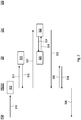
- FIG. 2 shown schematically receives the proxy 10 via the contactless interface RF / 12 of the reader 14 / PCD at S10 a request to perform a security operation according to the first application CA1 (client applet 1).
- the proxy 10 then causes the signal associated with the requested first application CA1 to be displayed via the signal display 20.
- the proxy 10 then waits for an acknowledgment from the user requesting execution of the application CA1 displayed via the signal display 20. This can be done, for example, by entering an identifier (for example on the card), such as a PIN or the like, on the basis of which an authentication of the user can be made, or alternatively by a separate direct confirmation.
- an identifier for example on the card
- the proxy 10 forwards S14 the received PIN for review to the authorization manager CM.
- the authorization manager CM checks the PIN and gives a positive response to the proxy 10 at S18.
- the authentication status of the PIN is set to "TRUE" within the card.
- the displayed application is thus the user authentication initiated in one gear.
- the proxy 10 sends an execution command to the first application CA1 at S20.
- the application CA1 in response to this execution command, generates a request for the authentication status of the PIN at S22 and sends this request to the authorization manager CM at S24.
- the authorization manager CM asks at S26 Authentication status of the PIN and S28 sends the result of the query / verification (Okay / TRUE) to the application CA1, which is thus released (at least implicitly) and then starts the execution.
- the execution result is transmitted from the application CA1 to the proxy 10 at S30.
- the proxy 10 transmits a de-authentication command to the authorization manager CM at S32, which then sets the authentication status of the PIN to "not set” or "FALSE", and at S34 sends the corresponding acknowledgment to the proxy 10 which in turn causes the proxy 10 to send the result of the application execution to the reader / terminal PCD at S36 (for example, if it were a physical access by a gate or a door, the result would be the application CA1 noting that the authenticated user is authorized to access the gate and how to open the door, and the terminal would receive a door open command from the smart card (ie, its proxy).
- FIG. 3 schematically illustrates a corresponding flow for a variant in which so-called application-specific pseudo-authentication objects are provided.
- the authorization manager CM is then configured so that when entering an identifier in response to a reproduced via the signal display application internally with the pseudo identifier assigned to this application works and this after input of the identifier by the user and positive identification verification (ie authentication ) sets to "true").
- the authorization manager CM is configured such that an authentication status is not set in connection with the user PIN, but for the internal pseudo-PINs pPIN1 and pPIN2.
- the proxy 10 receives via the contactless interface RF / 12 from the reader 14 / PCD at S50 a request to perform a security operation according to the first application CA1 (client applet 1). The proxy 10 then causes S52 to display, via the signal display 20, the signal associated with the requested first application CA1.
- the proxy 10 then waits for an acknowledgment from the user requesting execution of the application CA1 displayed via the signal display 20. This is done as already in connection with the embodiment of FIG. 2 written by entering an identifier (eg on the card), such as a PIN or the like, on the basis of which an authentication of the user can be made.
- an identifier eg on the card
- the proxy 10 After receiving the PIN, the proxy 10 forwards the received PIN at S54 to the authorization manager CM for the specific application CA1, so that the authorization manager CM checks the entered user PIN at S56 with the pseudo-PIN pPIN1 assigned to the requested application CA1 , If the user PIN (and associated authentication) is checked positively, the authorization manager CM sets the authentication status of the pseudo-PIN pPIN1 to "TRUE" and sends a positive acknowledgment to the proxy 10 at S58.
- the proxy 10 sends an execution command to the first application CA1 at S60.
- the application CA1 in response to this execution command, generates a request for the authentication status of "its" pseudo-PIN pPIN1 at S62 and sends this request to the authorization manager CM at S64.
- the authorization manager CM queries the authentication status of the pPIN1 at S66 and sends the result of the query (OK / TRUE) to the application CA1 at S68, which is thus released (at least implicitly) and then starts execution.
- the execution result is output directly from the application CA1 via the proxy 10 (to the reading device PCD) at S70.
- the process deviates from the above in connection with the embodiment of FIG. 2 From there, the result is first transmitted internally to the proxy 10, which then causes the de-authentication of the PIN at the authorization administrator CM. Only then is the starting example of the FIG. 2 the result given "outwards".
- the internal pseudo-authentication objects pPIN1 and pPIN2 it is ensured that only the pseudo-authentication object has a positive authentication status assigned to the desired application while the remaining pseudo-authentication object (s) are not set.
- the "precautionary measure" of the preceding de-authentication can thus be dispensed with so that, as described, the application result can be output directly.
- a request for the execution of the second application CA2 is sent directly to the application CA2 by the reading device PCD at S80 (abusive).
- the application CA2 in response, generates a request for the authentication status of its pseudo PIN, pPIN2, and sends this request to the authorization manager CM at S84.
- the authorization manager CM queries the authentication status of the pPIN2 at S86 and sends the result of the query ("FALSE" / unauthenticated) to the application CA2 at S88, which is thus not released and does not start execution. Rather, the application CA2 sends a non-execution message (such as security status not satisfied) to the PCD reader at S90.
- APDU application protocol data unit; software data container in which the data of an application are packaged to be exchanged between the reader / terminal and the chip card).
- APDU application protocol data unit
- a binding to a single APDU for one-time authentication can take place.
- the input on the card could be just an authorization instead of an authentication.
- the user therefore sees what the card is to be used for, but the application does not require explicit authentication, but the user nevertheless recognizes (for example by means of an LED) which transaction is to be carried out and confirms this by means of a type of "confirm" key. Enter key.
- a single usage possibility of an application CA x can be signaled.
- the invention thus prevents misuse of applications on multifunctional smart cards by preventing abusive execution of an application not desired by the user.
- the non-selected application is thus (temporarily) locked.
- the user can be sure that his user authentication will only be used in connection with a certain application and will not be abused for other applications. It is an application-based user authentication via feedback via a signal display in multifunctional smart cards.
Landscapes
- Engineering & Computer Science (AREA)
- Computer Hardware Design (AREA)
- Computer Security & Cryptography (AREA)
- General Engineering & Computer Science (AREA)
- Microelectronics & Electronic Packaging (AREA)
- Physics & Mathematics (AREA)
- General Physics & Mathematics (AREA)
- Theoretical Computer Science (AREA)
- Storage Device Security (AREA)
Applications Claiming Priority (1)
| Application Number | Priority Date | Filing Date | Title |
|---|---|---|---|
| DE102017223509.8A DE102017223509A1 (de) | 2017-12-21 | 2017-12-21 | Prozessorchipkarte und ein Verfahren zu deren Betrieb |
Publications (2)
| Publication Number | Publication Date |
|---|---|
| EP3502971A1 true EP3502971A1 (fr) | 2019-06-26 |
| EP3502971B1 EP3502971B1 (fr) | 2020-11-18 |
Family
ID=64959149
Family Applications (1)
| Application Number | Title | Priority Date | Filing Date |
|---|---|---|---|
| EP18214309.9A Active EP3502971B1 (fr) | 2017-12-21 | 2018-12-20 | Carte à puce de processeur et son procédé de fonctionnement |
Country Status (2)
| Country | Link |
|---|---|
| EP (1) | EP3502971B1 (fr) |
| DE (1) | DE102017223509A1 (fr) |
Citations (5)
| Publication number | Priority date | Publication date | Assignee | Title |
|---|---|---|---|---|
| DE202010006698U1 (de) * | 2009-05-13 | 2010-08-26 | Lorenzen, Karsten | Chipkarte mit optischer Meldefunktion |
| US20150262052A1 (en) * | 2014-03-14 | 2015-09-17 | Ebay Inc. | Omni smart card |
| US9230255B1 (en) * | 2014-08-15 | 2016-01-05 | Mastercard International Incorporated | Payment card having light-emitting diode indicators coordinated with stored payment applications |
| EP3009966A1 (fr) * | 2005-02-17 | 2016-04-20 | Koninklijke Philips N.V. | Carte à puce et son procédé de fonctionnement |
| EP3214583A2 (fr) * | 2016-03-04 | 2017-09-06 | Bundesdruckerei GmbH | Document de sécurité ou de valeur comprenant un capteur de détection d'une interaction d'utilisateur et d'un circuit électronique |
Family Cites Families (2)
| Publication number | Priority date | Publication date | Assignee | Title |
|---|---|---|---|---|
| DE19610070A1 (de) | 1996-03-14 | 1997-09-18 | Siemens Ag | Chipkarte |
| DE19839041C2 (de) | 1998-08-28 | 2003-03-27 | Ibm | Verfahren zum Identifizieren und Darstellen von Zuständen eines Fehlbedienungszählers |
-
2017
- 2017-12-21 DE DE102017223509.8A patent/DE102017223509A1/de not_active Withdrawn
-
2018
- 2018-12-20 EP EP18214309.9A patent/EP3502971B1/fr active Active
Patent Citations (5)
| Publication number | Priority date | Publication date | Assignee | Title |
|---|---|---|---|---|
| EP3009966A1 (fr) * | 2005-02-17 | 2016-04-20 | Koninklijke Philips N.V. | Carte à puce et son procédé de fonctionnement |
| DE202010006698U1 (de) * | 2009-05-13 | 2010-08-26 | Lorenzen, Karsten | Chipkarte mit optischer Meldefunktion |
| US20150262052A1 (en) * | 2014-03-14 | 2015-09-17 | Ebay Inc. | Omni smart card |
| US9230255B1 (en) * | 2014-08-15 | 2016-01-05 | Mastercard International Incorporated | Payment card having light-emitting diode indicators coordinated with stored payment applications |
| EP3214583A2 (fr) * | 2016-03-04 | 2017-09-06 | Bundesdruckerei GmbH | Document de sécurité ou de valeur comprenant un capteur de détection d'une interaction d'utilisateur et d'un circuit électronique |
Also Published As
| Publication number | Publication date |
|---|---|
| EP3502971B1 (fr) | 2020-11-18 |
| DE102017223509A1 (de) | 2019-06-27 |
Similar Documents
| Publication | Publication Date | Title |
|---|---|---|
| EP2454704B1 (fr) | Methode pour lir des attributes de un jeton d'identite | |
| EP3731119B1 (fr) | Procédé mis en uvre par ordinateur destiné au contrôle d'accès | |
| EP3261011B1 (fr) | Procédé de lecture d'attributs à partir d'un jeton d'identification | |
| EP2769330B1 (fr) | Procédé d'appel d'un programme client | |
| EP2415228B1 (fr) | Procede de lecture des attributes d'un token utilisant une connexion radio | |
| EP3699791B1 (fr) | Contrôle d'accès comprenant un appareil radio mobile | |
| EP3748521B1 (fr) | Méthode pour lire les attributs d'un témoin d'identité | |
| EP2602738A2 (fr) | Dispositif de protection des mécanismes de sécurité contre la malveillance | |
| WO2013056783A1 (fr) | Terminal mobile, terminal de transactions et procédé de réalisation d'une transaction à partir d'un terminal de transactions en utilisant un terminal mobile | |
| EP3254432B1 (fr) | Procédé de gestion d'autorisation dans un ensemble comportant plusieurs systèmes informatiques | |
| EP2996299B1 (fr) | Procédé et système d'autorisation d'une action sur un système auto-commandé | |
| EP3319003A1 (fr) | Procédé et système d'authentification d'un appareil de télécommunication mobile sur un système informatique de service et appareil de télécommunication mobile | |
| EP2752785B1 (fr) | Procédé de personnalisation d'un élément sécurisé (Secure Element SE) et système informatique | |
| EP2916252B1 (fr) | Procédé de transaction électronique et système informatique | |
| EP3657750B1 (fr) | Procédé d'authentification des lunettes intelligentes dans un réseau de données | |
| EP3244331B1 (fr) | Procédé de lecture d'attributs à partir d'un jeton d'identification | |
| EP3502971B1 (fr) | Carte à puce de processeur et son procédé de fonctionnement | |
| EP2169579B1 (fr) | Procédé et dispositif d'accès à un document lisible sur machine | |
| EP3298526B1 (fr) | Procédé de lecture d'attributs à partir d'un jeton d'identification | |
| EP2893483B1 (fr) | Procédé de personnalisation d'un élément sécurisé (se) et système informatique | |
| EP3283999B1 (fr) | Système électronique servant à produire un certificat | |
| EP1365363B1 (fr) | Méthode pour effectuer des transactions de données à l'aide d'un dispositif de transaction comportant un composant principal et un composant annexe séparable | |
| EP3361436B1 (fr) | Procédé d'autorisation d'une transaction | |
| EP2840757B1 (fr) | Administration individuelle et centrale des cartes de puce | |
| DE102013022448B3 (de) | Elektronisches Transaktionsverfahren und Computersystem |
Legal Events
| Date | Code | Title | Description |
|---|---|---|---|
| PUAI | Public reference made under article 153(3) epc to a published international application that has entered the european phase |
Free format text: ORIGINAL CODE: 0009012 |
|
| STAA | Information on the status of an ep patent application or granted ep patent |
Free format text: STATUS: THE APPLICATION HAS BEEN PUBLISHED |
|
| AK | Designated contracting states |
Kind code of ref document: A1 Designated state(s): AL AT BE BG CH CY CZ DE DK EE ES FI FR GB GR HR HU IE IS IT LI LT LU LV MC MK MT NL NO PL PT RO RS SE SI SK SM TR |
|
| AX | Request for extension of the european patent |
Extension state: BA ME |
|
| STAA | Information on the status of an ep patent application or granted ep patent |
Free format text: STATUS: REQUEST FOR EXAMINATION WAS MADE |
|
| 17P | Request for examination filed |
Effective date: 20191108 |
|
| RBV | Designated contracting states (corrected) |
Designated state(s): AL AT BE BG CH CY CZ DE DK EE ES FI FR GB GR HR HU IE IS IT LI LT LU LV MC MK MT NL NO PL PT RO RS SE SI SK SM TR |
|
| STAA | Information on the status of an ep patent application or granted ep patent |
Free format text: STATUS: EXAMINATION IS IN PROGRESS |
|
| 17Q | First examination report despatched |
Effective date: 20200615 |
|
| GRAP | Despatch of communication of intention to grant a patent |
Free format text: ORIGINAL CODE: EPIDOSNIGR1 |
|
| STAA | Information on the status of an ep patent application or granted ep patent |
Free format text: STATUS: GRANT OF PATENT IS INTENDED |
|
| INTG | Intention to grant announced |
Effective date: 20200723 |
|
| RIN1 | Information on inventor provided before grant (corrected) |
Inventor name: KRAUS, MICHA Inventor name: BASTIAN, PAUL |
|
| GRAS | Grant fee paid |
Free format text: ORIGINAL CODE: EPIDOSNIGR3 |
|
| GRAA | (expected) grant |
Free format text: ORIGINAL CODE: 0009210 |
|
| STAA | Information on the status of an ep patent application or granted ep patent |
Free format text: STATUS: THE PATENT HAS BEEN GRANTED |
|
| AK | Designated contracting states |
Kind code of ref document: B1 Designated state(s): AL AT BE BG CH CY CZ DE DK EE ES FI FR GB GR HR HU IE IS IT LI LT LU LV MC MK MT NL NO PL PT RO RS SE SI SK SM TR |
|
| REG | Reference to a national code |
Ref country code: GB Ref legal event code: FG4D Free format text: NOT ENGLISH |
|
| REG | Reference to a national code |
Ref country code: CH Ref legal event code: NV Representative=s name: VALIPAT S.A. C/O BOVARD SA NEUCHATEL, CH Ref country code: CH Ref legal event code: EP |
|
| REG | Reference to a national code |
Ref country code: DE Ref legal event code: R096 Ref document number: 502018003044 Country of ref document: DE |
|
| REG | Reference to a national code |
Ref country code: IE Ref legal event code: FG4D Free format text: LANGUAGE OF EP DOCUMENT: GERMAN |
|
| REG | Reference to a national code |
Ref country code: AT Ref legal event code: REF Ref document number: 1336575 Country of ref document: AT Kind code of ref document: T Effective date: 20201215 |
|
| REG | Reference to a national code |
Ref country code: NL Ref legal event code: FP |
|
| PG25 | Lapsed in a contracting state [announced via postgrant information from national office to epo] |
Ref country code: RS Free format text: LAPSE BECAUSE OF FAILURE TO SUBMIT A TRANSLATION OF THE DESCRIPTION OR TO PAY THE FEE WITHIN THE PRESCRIBED TIME-LIMIT Effective date: 20201118 Ref country code: PT Free format text: LAPSE BECAUSE OF FAILURE TO SUBMIT A TRANSLATION OF THE DESCRIPTION OR TO PAY THE FEE WITHIN THE PRESCRIBED TIME-LIMIT Effective date: 20210318 Ref country code: FI Free format text: LAPSE BECAUSE OF FAILURE TO SUBMIT A TRANSLATION OF THE DESCRIPTION OR TO PAY THE FEE WITHIN THE PRESCRIBED TIME-LIMIT Effective date: 20201118 Ref country code: NO Free format text: LAPSE BECAUSE OF FAILURE TO SUBMIT A TRANSLATION OF THE DESCRIPTION OR TO PAY THE FEE WITHIN THE PRESCRIBED TIME-LIMIT Effective date: 20210218 Ref country code: GR Free format text: LAPSE BECAUSE OF FAILURE TO SUBMIT A TRANSLATION OF THE DESCRIPTION OR TO PAY THE FEE WITHIN THE PRESCRIBED TIME-LIMIT Effective date: 20210219 |
|
| PG25 | Lapsed in a contracting state [announced via postgrant information from national office to epo] |
Ref country code: BG Free format text: LAPSE BECAUSE OF FAILURE TO SUBMIT A TRANSLATION OF THE DESCRIPTION OR TO PAY THE FEE WITHIN THE PRESCRIBED TIME-LIMIT Effective date: 20210218 Ref country code: SE Free format text: LAPSE BECAUSE OF FAILURE TO SUBMIT A TRANSLATION OF THE DESCRIPTION OR TO PAY THE FEE WITHIN THE PRESCRIBED TIME-LIMIT Effective date: 20201118 Ref country code: LV Free format text: LAPSE BECAUSE OF FAILURE TO SUBMIT A TRANSLATION OF THE DESCRIPTION OR TO PAY THE FEE WITHIN THE PRESCRIBED TIME-LIMIT Effective date: 20201118 Ref country code: PL Free format text: LAPSE BECAUSE OF FAILURE TO SUBMIT A TRANSLATION OF THE DESCRIPTION OR TO PAY THE FEE WITHIN THE PRESCRIBED TIME-LIMIT Effective date: 20201118 Ref country code: IS Free format text: LAPSE BECAUSE OF FAILURE TO SUBMIT A TRANSLATION OF THE DESCRIPTION OR TO PAY THE FEE WITHIN THE PRESCRIBED TIME-LIMIT Effective date: 20210318 |
|
| REG | Reference to a national code |
Ref country code: LT Ref legal event code: MG9D |
|
| PG25 | Lapsed in a contracting state [announced via postgrant information from national office to epo] |
Ref country code: HR Free format text: LAPSE BECAUSE OF FAILURE TO SUBMIT A TRANSLATION OF THE DESCRIPTION OR TO PAY THE FEE WITHIN THE PRESCRIBED TIME-LIMIT Effective date: 20201118 |
|
| PG25 | Lapsed in a contracting state [announced via postgrant information from national office to epo] |
Ref country code: LT Free format text: LAPSE BECAUSE OF FAILURE TO SUBMIT A TRANSLATION OF THE DESCRIPTION OR TO PAY THE FEE WITHIN THE PRESCRIBED TIME-LIMIT Effective date: 20201118 Ref country code: RO Free format text: LAPSE BECAUSE OF FAILURE TO SUBMIT A TRANSLATION OF THE DESCRIPTION OR TO PAY THE FEE WITHIN THE PRESCRIBED TIME-LIMIT Effective date: 20201118 Ref country code: SM Free format text: LAPSE BECAUSE OF FAILURE TO SUBMIT A TRANSLATION OF THE DESCRIPTION OR TO PAY THE FEE WITHIN THE PRESCRIBED TIME-LIMIT Effective date: 20201118 Ref country code: SK Free format text: LAPSE BECAUSE OF FAILURE TO SUBMIT A TRANSLATION OF THE DESCRIPTION OR TO PAY THE FEE WITHIN THE PRESCRIBED TIME-LIMIT Effective date: 20201118 Ref country code: CZ Free format text: LAPSE BECAUSE OF FAILURE TO SUBMIT A TRANSLATION OF THE DESCRIPTION OR TO PAY THE FEE WITHIN THE PRESCRIBED TIME-LIMIT Effective date: 20201118 Ref country code: EE Free format text: LAPSE BECAUSE OF FAILURE TO SUBMIT A TRANSLATION OF THE DESCRIPTION OR TO PAY THE FEE WITHIN THE PRESCRIBED TIME-LIMIT Effective date: 20201118 |
|
| REG | Reference to a national code |
Ref country code: DE Ref legal event code: R097 Ref document number: 502018003044 Country of ref document: DE |
|
| PG25 | Lapsed in a contracting state [announced via postgrant information from national office to epo] |
Ref country code: MC Free format text: LAPSE BECAUSE OF FAILURE TO SUBMIT A TRANSLATION OF THE DESCRIPTION OR TO PAY THE FEE WITHIN THE PRESCRIBED TIME-LIMIT Effective date: 20201118 Ref country code: DK Free format text: LAPSE BECAUSE OF FAILURE TO SUBMIT A TRANSLATION OF THE DESCRIPTION OR TO PAY THE FEE WITHIN THE PRESCRIBED TIME-LIMIT Effective date: 20201118 |
|
| REG | Reference to a national code |
Ref country code: BE Ref legal event code: MM Effective date: 20201231 |
|
| PLBE | No opposition filed within time limit |
Free format text: ORIGINAL CODE: 0009261 |
|
| STAA | Information on the status of an ep patent application or granted ep patent |
Free format text: STATUS: NO OPPOSITION FILED WITHIN TIME LIMIT |
|
| 26N | No opposition filed |
Effective date: 20210819 |
|
| PG25 | Lapsed in a contracting state [announced via postgrant information from national office to epo] |
Ref country code: AL Free format text: LAPSE BECAUSE OF FAILURE TO SUBMIT A TRANSLATION OF THE DESCRIPTION OR TO PAY THE FEE WITHIN THE PRESCRIBED TIME-LIMIT Effective date: 20201118 Ref country code: IE Free format text: LAPSE BECAUSE OF NON-PAYMENT OF DUE FEES Effective date: 20201220 Ref country code: IT Free format text: LAPSE BECAUSE OF FAILURE TO SUBMIT A TRANSLATION OF THE DESCRIPTION OR TO PAY THE FEE WITHIN THE PRESCRIBED TIME-LIMIT Effective date: 20201118 Ref country code: LU Free format text: LAPSE BECAUSE OF NON-PAYMENT OF DUE FEES Effective date: 20201220 |
|
| PG25 | Lapsed in a contracting state [announced via postgrant information from national office to epo] |
Ref country code: SI Free format text: LAPSE BECAUSE OF FAILURE TO SUBMIT A TRANSLATION OF THE DESCRIPTION OR TO PAY THE FEE WITHIN THE PRESCRIBED TIME-LIMIT Effective date: 20201118 |
|
| PG25 | Lapsed in a contracting state [announced via postgrant information from national office to epo] |
Ref country code: ES Free format text: LAPSE BECAUSE OF FAILURE TO SUBMIT A TRANSLATION OF THE DESCRIPTION OR TO PAY THE FEE WITHIN THE PRESCRIBED TIME-LIMIT Effective date: 20201118 |
|
| PG25 | Lapsed in a contracting state [announced via postgrant information from national office to epo] |
Ref country code: IS Free format text: LAPSE BECAUSE OF FAILURE TO SUBMIT A TRANSLATION OF THE DESCRIPTION OR TO PAY THE FEE WITHIN THE PRESCRIBED TIME-LIMIT Effective date: 20210318 Ref country code: TR Free format text: LAPSE BECAUSE OF FAILURE TO SUBMIT A TRANSLATION OF THE DESCRIPTION OR TO PAY THE FEE WITHIN THE PRESCRIBED TIME-LIMIT Effective date: 20201118 Ref country code: MT Free format text: LAPSE BECAUSE OF FAILURE TO SUBMIT A TRANSLATION OF THE DESCRIPTION OR TO PAY THE FEE WITHIN THE PRESCRIBED TIME-LIMIT Effective date: 20201118 Ref country code: CY Free format text: LAPSE BECAUSE OF FAILURE TO SUBMIT A TRANSLATION OF THE DESCRIPTION OR TO PAY THE FEE WITHIN THE PRESCRIBED TIME-LIMIT Effective date: 20201118 |
|
| PG25 | Lapsed in a contracting state [announced via postgrant information from national office to epo] |
Ref country code: MK Free format text: LAPSE BECAUSE OF FAILURE TO SUBMIT A TRANSLATION OF THE DESCRIPTION OR TO PAY THE FEE WITHIN THE PRESCRIBED TIME-LIMIT Effective date: 20201118 |
|
| PG25 | Lapsed in a contracting state [announced via postgrant information from national office to epo] |
Ref country code: BE Free format text: LAPSE BECAUSE OF NON-PAYMENT OF DUE FEES Effective date: 20201231 |
|
| P01 | Opt-out of the competence of the unified patent court (upc) registered |
Effective date: 20230526 |
|
| REG | Reference to a national code |
Ref country code: CH Ref legal event code: U11 Free format text: ST27 STATUS EVENT CODE: U-0-0-U10-U11 (AS PROVIDED BY THE NATIONAL OFFICE) Effective date: 20260101 |
|
| PGFP | Annual fee paid to national office [announced via postgrant information from national office to epo] |
Ref country code: GB Payment date: 20251218 Year of fee payment: 8 |
|
| PGFP | Annual fee paid to national office [announced via postgrant information from national office to epo] |
Ref country code: AT Payment date: 20251215 Year of fee payment: 8 |
|
| PGFP | Annual fee paid to national office [announced via postgrant information from national office to epo] |
Ref country code: FR Payment date: 20251218 Year of fee payment: 8 Ref country code: NL Payment date: 20251217 Year of fee payment: 8 |
|
| PGFP | Annual fee paid to national office [announced via postgrant information from national office to epo] |
Ref country code: DE Payment date: 20251222 Year of fee payment: 8 |
|
| PGFP | Annual fee paid to national office [announced via postgrant information from national office to epo] |
Ref country code: CH Payment date: 20260101 Year of fee payment: 8 |