EP3504754B1 - Méta-surface accordable à cristaux liquides pour antennes de direction de faisceau - Google Patents
Méta-surface accordable à cristaux liquides pour antennes de direction de faisceau Download PDFInfo
- Publication number
- EP3504754B1 EP3504754B1 EP17852272.8A EP17852272A EP3504754B1 EP 3504754 B1 EP3504754 B1 EP 3504754B1 EP 17852272 A EP17852272 A EP 17852272A EP 3504754 B1 EP3504754 B1 EP 3504754B1
- Authority
- EP
- European Patent Office
- Prior art keywords
- metasurface
- microstrip
- substrate
- array
- microstrip patch
- Prior art date
- Legal status (The legal status is an assumption and is not a legal conclusion. Google has not performed a legal analysis and makes no representation as to the accuracy of the status listed.)
- Active
Links
Images



Classifications
-
- H—ELECTRICITY
- H01—ELECTRIC ELEMENTS
- H01Q—ANTENNAS, i.e. RADIO AERIALS
- H01Q15/00—Devices for reflection, refraction, diffraction or polarisation of waves radiated from an antenna, e.g. quasi-optical devices
- H01Q15/14—Reflecting surfaces; Equivalent structures
- H01Q15/148—Reflecting surfaces; Equivalent structures with means for varying the reflecting properties
-
- H—ELECTRICITY
- H01—ELECTRIC ELEMENTS
- H01Q—ANTENNAS, i.e. RADIO AERIALS
- H01Q1/00—Details of, or arrangements associated with, antennas
- H01Q1/36—Structural form of radiating elements, e.g. cone, spiral, umbrella; Particular materials used therewith
-
- H—ELECTRICITY
- H01—ELECTRIC ELEMENTS
- H01Q—ANTENNAS, i.e. RADIO AERIALS
- H01Q1/00—Details of, or arrangements associated with, antennas
- H01Q1/36—Structural form of radiating elements, e.g. cone, spiral, umbrella; Particular materials used therewith
- H01Q1/364—Structural form of radiating elements, e.g. cone, spiral, umbrella; Particular materials used therewith using a particular conducting material, e.g. superconductor
-
- H—ELECTRICITY
- H01—ELECTRIC ELEMENTS
- H01Q—ANTENNAS, i.e. RADIO AERIALS
- H01Q15/00—Devices for reflection, refraction, diffraction or polarisation of waves radiated from an antenna, e.g. quasi-optical devices
- H01Q15/0006—Devices acting selectively as reflecting surface, as diffracting or as refracting device, e.g. frequency filtering or angular spatial filtering devices
- H01Q15/0013—Devices acting selectively as reflecting surface, as diffracting or as refracting device, e.g. frequency filtering or angular spatial filtering devices said selective devices working as frequency-selective reflecting surfaces, e.g. FSS, dichroic plates, surfaces being partly transmissive and reflective
- H01Q15/002—Devices acting selectively as reflecting surface, as diffracting or as refracting device, e.g. frequency filtering or angular spatial filtering devices said selective devices working as frequency-selective reflecting surfaces, e.g. FSS, dichroic plates, surfaces being partly transmissive and reflective said selective devices being reconfigurable or tunable, e.g. using switches or diodes
-
- H—ELECTRICITY
- H01—ELECTRIC ELEMENTS
- H01Q—ANTENNAS, i.e. RADIO AERIALS
- H01Q15/00—Devices for reflection, refraction, diffraction or polarisation of waves radiated from an antenna, e.g. quasi-optical devices
- H01Q15/0006—Devices acting selectively as reflecting surface, as diffracting or as refracting device, e.g. frequency filtering or angular spatial filtering devices
- H01Q15/0013—Devices acting selectively as reflecting surface, as diffracting or as refracting device, e.g. frequency filtering or angular spatial filtering devices said selective devices working as frequency-selective reflecting surfaces, e.g. FSS, dichroic plates, surfaces being partly transmissive and reflective
- H01Q15/0026—Devices acting selectively as reflecting surface, as diffracting or as refracting device, e.g. frequency filtering or angular spatial filtering devices said selective devices working as frequency-selective reflecting surfaces, e.g. FSS, dichroic plates, surfaces being partly transmissive and reflective said selective devices having a stacked geometry or having multiple layers
-
- H—ELECTRICITY
- H01—ELECTRIC ELEMENTS
- H01Q—ANTENNAS, i.e. RADIO AERIALS
- H01Q15/00—Devices for reflection, refraction, diffraction or polarisation of waves radiated from an antenna, e.g. quasi-optical devices
- H01Q15/0006—Devices acting selectively as reflecting surface, as diffracting or as refracting device, e.g. frequency filtering or angular spatial filtering devices
- H01Q15/0013—Devices acting selectively as reflecting surface, as diffracting or as refracting device, e.g. frequency filtering or angular spatial filtering devices said selective devices working as frequency-selective reflecting surfaces, e.g. FSS, dichroic plates, surfaces being partly transmissive and reflective
- H01Q15/004—Devices acting selectively as reflecting surface, as diffracting or as refracting device, e.g. frequency filtering or angular spatial filtering devices said selective devices working as frequency-selective reflecting surfaces, e.g. FSS, dichroic plates, surfaces being partly transmissive and reflective using superconducting materials or magnetised substrates
-
- H—ELECTRICITY
- H01—ELECTRIC ELEMENTS
- H01Q—ANTENNAS, i.e. RADIO AERIALS
- H01Q3/00—Arrangements for changing or varying the orientation or the shape of the directional pattern of the waves radiated from an antenna or antenna system
- H01Q3/26—Arrangements for changing or varying the orientation or the shape of the directional pattern of the waves radiated from an antenna or antenna system varying the relative phase or relative amplitude of energisation between two or more active radiating elements; varying the distribution of energy across a radiating aperture
- H01Q3/30—Arrangements for changing or varying the orientation or the shape of the directional pattern of the waves radiated from an antenna or antenna system varying the relative phase or relative amplitude of energisation between two or more active radiating elements; varying the distribution of energy across a radiating aperture varying the relative phase between the radiating elements of an array
-
- H—ELECTRICITY
- H01—ELECTRIC ELEMENTS
- H01Q—ANTENNAS, i.e. RADIO AERIALS
- H01Q3/00—Arrangements for changing or varying the orientation or the shape of the directional pattern of the waves radiated from an antenna or antenna system
- H01Q3/44—Arrangements for changing or varying the orientation or the shape of the directional pattern of the waves radiated from an antenna or antenna system varying the electric or magnetic characteristics of reflecting, refracting, or diffracting devices associated with the radiating element
- H01Q3/46—Active lenses or reflecting arrays
Definitions
- the present disclosure relates to antennas.
- the present disclosure relates to a liquid-crystal tunable metasurface for beam steering antennas.
- Signal strength in an antenna system is dependent on a number of factors, such as distance from the receiver to the transmitter, obstacles between the transmitter and receiver, signal fading, multipath reception, line of sight interference, Fresnel zone interference, radio frequency (RF) interference, weather conditions, noise, etc. Any one, or a combination, of these factors may result in poor connections, dropped connections, low data rates, high latency, etc.
- a lobe of a radiation pattern for the transmitter antenna and/or the receiver antenna may be adjusted to direct the lobe between the receiver and the transmitter.
- Adaptive beam formers or beam steering automatically adapts the antenna response (of the transmitter, receiver, or both) to compensate for signal loss.
- interfering and constructing patterns may be used to change the shape and direction of the signal beam from multiple antennas using antenna spacing and the phase of signal emission from each antenna in an antenna array.
- Beam steering may change the directionality of the main lobe by controlling the phase and relative amplitude of the signal at each transmitter.
- a metasurface which is an artificial sheet material having electromagnetic properties that can varied on demand, may control reflection and transmission characteristics of EM wave.
- a metasurface can be a two-dimensional periodical structure that contains electrically small scatterers with periodicity relatively small compared to an operating wavelength.
- a metasurface for purposes of beam steering system is described in " Two-Dimensional Beam Steering Using an Electrically Tunable Impedance Surface” by Sievenpiper et al. (IEEE Trans. On Antennas and Prop., Vol. 51, No. 10, pp 2713-2721, October, 2003 ).
- Sievenpiper discloses a two-dimensioning beam steering using an electrically tunable impedance surface loaded using varactor diodes.
- varactor diode loading becomes impractical for high frequencies with a large surface where over hundreds of diodes are required.
- use of varactor diodes may be undesirable due to its nonlinearity which can induce undesirable noise due to passive intermodulation (PIM).
- PIM passive intermodulation
- Patent US6552696B1 has disclosed a tuneable impedance surface for steering and/or focusing a radio frequency beam.
- the tunable surface comprises a ground plane; a plurality of elements disposed a distance from the ground plane, the distance being less than a wavelength of the radio frequency beam; and a capacitor arrangement for controllably varying the capacitance of adjacent top plates, the capacitor arrangement including a dielectric material which locally changes its dielectric constant in response to an external stimulus.
- Example embodiments are described of an electronically tunable metasurface whose reflective phase can be electronically reconfigured to allow effective antenna beam steering.
- the metasurface includes first and second double sided substrates defining an intermediate region between them containing liquid crystal in a nematic phase.
- the first substrate has a first microstrip patch array formed on a side thereof that faces the second substrate, the first microstrip patch array comprising a two-dimensional array of microstrip patches each being electrically connected to a common potential.
- the second double sided substrate has a second microstrip patch array formed on a side thereof that faces the first substrate, the second microstrip patch array comprising a two-dimensional array of microstrip patches each having a respective conductive terminal.
- the first microstrip patch array and the second microstrip patch array are aligned to form a two dimensional array of cells, each cell comprising a microstrip patch of the first microstrip patch array arranged in spaced apart opposition to a microstrip patch of the second microstrip patch array with a volume of the liquid crystal located therebetween.
- the conductive terminal to the microstrip patch of the microstrip patch second array permitting a control voltage to be applied to the cell to control a dielectric value of the volume of the liquid crystal, thereby permitting a reflection phase of the cell to be selectively tuned.
- the metasurface further includes a gridded wire mesh on the first substrate, each of the microstrip patches of the first microstrip patch array being electrically connected to a respective point of the gridded wire mesh to provide the common potential.
- the gridded wire mesh may be formed on a side of the first substrate that is opposite the side on which the first microstrip patch array is formed, each of the microstrip patches of the first microstrip patch array being electrically connected to the gridded wire mesh by a respective plated through hole that extends through the first substrate.
- the respective conductive terminals that extend through the second substrate may also each be plated through holes.
- a thickness of the first substrate and a thickness of the intermediate region containing the liquid crystal are each less than 1/4 of an intended minimum operating wavelength of the incident wave.
- the method includes providing a metasurface to reflect an incident wave from an antenna, the metasurface comprising a two dimensional array of cells each including a volume of liquid crystal; applying voltages to control terminals associated with a plurality of the cells of the metasurface, the voltage orienting molecules of a liquid crystal within each cell; and adjusting the phase of the incident wave by adjusting a resonant frequency of each cell by varying the orientation of the molecules.
- Providing a metasurface also includes: providing a first printed circuit board (PCB) having an intermediate substrate layer with a first two dimensional array of microstrip patches formed on one side of the substrate layer and a gridded wire mesh formed on an opposite side of the substrate layer, each of the microstrip patches of the first two dimensional array be electrically connected to a respective point on the wire mesh by a conductor extending through the intermediate substrate layer; providing a second PCB having an intermediate substrate layer with a second two dimensional array of microstrip patches formed on one side of the substrate layer, each of the microstrip patches of the second two dimensional array having a respective conductive control terminal that extends through the second substrate; and arranging the first PCB and the second PCB with a layer of nematic state liquid crystal therebetween such that the microstrip patches of the first two dimensional array each align with a respective microstrip patch of the second two dimensional array to form the two dimensional array of cells.
- PCB printed circuit board
- the metasurface 100 is a liquid-crystal-loaded tunable sheet providing a reflective phase that can be electronically reconfigured to allow effective antenna beam steering.
- the metasurface 100 is a high-impedance surface and includes an upper surface or side 102 (shown in FIG. 1 ), a bottom surface or side 104 (shown in FIG. 2 ), and includes an array of addressable cells 106 for reflective beam steering antenna applications.
- the cells 106 are arranged to provide a two-dimensional periodical structure implementing an array of electrically small scatterers.
- the dimensions of the cells 106 are selected such that the periodicity of the cell array is relatively small compared to the operating wavelength of the radio waves that the metasurface 100 is intended to reflect. In some examples, the cells have a periodicity that is less than a quarter of the minimum intended operating wavelength.
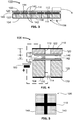
- FIG. 3 illustrates a side sectional view of a row of cells 106 of metasurface 100
- FIG. 4 shows an enlarged side sectional view of one of the cells 106 as indicated by dashed box 4 in FIG. 3
- the metasurface 100 includes an upper multi-layer double-sided printed circuit board (PCB) 120 and a lower multi-layer double sided PCB 122, which respectively define the upper and bottom sides 102, 104.
- a sub-operating wavelength layer of electronically tunable liquid crystal (LC) 146 is located between the upper and lower PCBs 120,122.
- LC electronically tunable liquid crystal
- Upper PCB 120 has a central non-conductive substrate layer (shown in cross-hatch in FIGs. 3 and 4 ).
- a gridded wire mesh 118 forms the top layer of the PCB 120, and a two dimensional array of conductive microstrip patches 140, each of which is surrounded by an insulating slot or gap 148, forms the bottom layer of the PCB 120.
- each microstrip patch 140 is electrically connected by a conductive plated-through hole (PTH) via 112 that extends from the center of the patch 140 through the PCB 120 substrate layer to a respective intersection point of wire mesh 118 such that wire mesh 118 provides a common DC return path for each of the microstrip patches 140.
- PTH conductive plated-through hole
- PTH vias 112 may be provided by forming and plating holes through the PCB 120 substrate layer
- microstrip patches 140 may be formed from etching gaps 148 from a conductive layer on the lower surface of PCB 120
- gridded wire mesh 118 may be similarly formed by etching a conductive layer on the upper layer of PCB 120.
- Lower PCB 122 has a central non-conductive substrate layer (shown in cross-hatch in FIGs. 3 and 4 ).
- a two dimensional array of conductive microstrip patches 142 which are each surrounded by an insulating slot or gap 148 and correspond in shape and periodicity to the upper PCB microstrip patches 140, form the top layer of lower PCB 122, and a conductive ground plane 130 forms the bottom layer of PCB 122.
- Each microstrip patch 142 is electrically connected to a respective conductive plated-through hole (PTH) via 114 that extends from the center of the patch 142 through the PCB 122 substrate layer to the ground plane 130 layer.
- PTH conductive plated-through hole
- the ground plane 130 includes an array of openings on the substrate layer that form a circular gap between the ground plane and the PTH vias 114 such that the ground plane 130 is electrically isolated from each of the PTH vias 114, permitting a unique control voltage to be applied to each PTH via 114.
- PTH vias 114 may be provided by forming and plating holes through the PCB 122 substrate layer
- microstrip patches 142 may be formed from etching gaps 148 from a conductive layer on the upper surface of PCB 120
- ground plane 130 may be similarly formed by etching a conductive layer on the lower layer of PCB 120 to provide insulated openings around each of the PTH vias 114.
- control voltages are provided to the lower microstrip patches 142 through PTH vias 114 that are accessible through the ground plane 130.
- Other embodiments could have different configurations, including a control line layer that could be integrated into substrate 122 to provide conductive control terminals to each of the microstrip patches 142.
- the upper and lower PCBs 120, 122 are located in spaced opposition to each other with an intermediate layer of liquid crystal 146 located between them.
- the upper PCB microstrip patches 140 and the lower PCB microstrip patches 142 align with each other to from an array of cell regions 144, each of which contains a volume of liquid crystal 146, thus providing an array of individually controllable, LC cell regions 144.
- each unit cell 106 includes a volume of tunable liquid crystal 146 that is located in region 144 between an upper conductive microstrip patch 140 and a lower conductive microstrip patch 142.
- Upper conductive microstrip patch 140 is connected by a respective conductive path (PTH via 112) to a common potential, namely wire mesh 118, and lower conductive microstrip patch 142 is connected to a control terminal (PTH via 114) that allows a unique control voltage from an adjustable DC voltage source 160 to be applied to the microstrip patch 142
- the metasurface 100 has a resonant frequency that can depend on the geometry of the cells 106 and dielectric properties of the materials used in the PCBs 120, 122.
- the microstrip patches 140, 142 have rectangular surfaces (for example square) having a maximum normal dimension that is less than 1 ⁇ 4 of the minimum intended operating wavelength, however other microstrip patch configurations could be used.
- the microstrip patches 140, 142 may have dimensions that are less than quarter of a wavelength of the intended operating wavelength of the metasurface 100.
- wire mesh 118 has a periodicity and grid dimensions that correspond to those of microstrip patches 140, with a grid intersection point occurring over a center point of each microstrip patch 140.
- the metasurface 100 illustrated in Figures 1 to 5 provides a structure in which etching can be used to form the components of PCB boards 120, 122.
- liquid crystal 146 is can be placed between the PCB's 120, 122, which can then be secured together.
- the liquid crystal 146 is a nematic liquid crystal that has an intermediate nematic gel-like state between solid crystalline and liquid phase at the intended operating temperature range of the metasurface 100.
- liquid crystal include, for example, GT3-23001 liquid crystal and BL038 liquid crystal from the Merck group.
- Liquid crystal 146 in a nematic state possesses dielectric anisotropy characteristics at microwave frequencies, whose effective dielectric constant may be adjusted by setting different orientations of the molecules of liquid crystal 146 relative to its reference axis.
- liquid crystal 146 comprises rod-like molecules 602 that orient parallel to an applied electric field ⁇ r .
- the liquid crystal 146 may change its dielectric properties due to different orientations of the molecules 602 caused by application of electrostatic field between the microstrip patches 140 and 142 as represented in the three images of FIG. 6 .
- the dielectric constant between the microstrip patches 140 and 142 at each unit cell 106 can be tuned by varying the DC voltage applied to patch 142.he reflection phase at each individual unit cell 106 to be controlled.
- the unit cells 106 can be collectively controlled so that metasurface 100 acts like a distributed spatial phase shifter that interacts with an incident wave and produces a reflected wave with varying phase shift across its aperture.
- An incident beam may be electronically steered to any 2D direction by changing the local electrostatic fields at each unit cell 106 location.
- each unit cell 106 may be tuned individually and electronically by adjusting DC voltage at each cell 106. Because reflection phase is determined by the frequency of the incoming wave with respect to the resonance frequency, the metasurface 100 can be tuned to form a distributed 2D phase shifter. Therefore, an incoming wave may be redirected by adjusting DC voltages of unit cells 106 to give proper phase distribution for the desired direction of reflected wave.
- the metasurface 100 has a relatively high density/small periodicity of cells 106 and can be analyzed as an effective medium with its surface impedance defined by effective lumped-element circuit parameters.
- ⁇ represents an minimum intended operating frequency
- top PCB 120 is relatively thin, having a thickness h1 ⁇ /20 and the liquid crystal 146 in cell region 144 has a thickness of h2 ⁇ /20 (i.e. the gap between the opposed microstrip patches 140 and 142).
- the thicknesses h1 and h2 can be different from each other.
- the bottom PCB 122 has a finite thickness h3 ⁇ ⁇ /4.
- FIGS. 7 and 8 illustrate equivalent circuits of the liquid crystal cell 106, where L and C1 are equivalent lump parameters as a result of the finite thickness of the bottom PCB 122.
- C v is the input capacitance of cell 106.
- the metasurface 100 reflects an incident wave with a phase shift of 180 degrees for frequency below the resonance frequency, and 0 degrees at the resonance frequency, and approaches -180 degrees for frequencies above the resonance frequency. Since the reflection phase may be determined by the frequency of the incoming wave with respect to the resonance frequency of the metasurface 100, the phase shift of the incoming wave can be adjusted for each individual cell 106 by varying the equivalent input capacitance C v of the unit cell 106, which is a function of the geometry of the microstrip patches 120 and 122, and thickness and dielectric constant of the liquid crystal layer 146.
- the effective dielectric constant of a unit cell 106 may be independently tuned by changing electrostatic voltage between microstrip patches 120 and 122 of the unit cell 106.
- This change in effective dielectric constant of a unit cell 106 leads to the change in the input capacitance, C v , of the cell 106.
- C v input capacitance
- a phase differential at various locations of the metasurface 100 may be changed individually.
- the structure of the unit cell 106 is simulated in FIGS. 9 and 10 using a full-wave finite element EM simulator, HFSS.
- FIG. 9 shows the simulated reflection amplitudes
- FIG. 10 shows the phases of the unit cell 106 for various effective dielectric constant values, ⁇ r , of the liquid crystal 146.
- the reflection phase of an incident wave at the surface of the metasurface 100 can be controlled by varying the DC voltages applied to unit cells 106 such that continuous beam steering of an EM wave can be achieved by regulating DC voltage distribution to unit cells 106 across the metasurface 100.
- example embodiments disclose individually addressable cells, other embodiments may have cells that may be addressable by row or column or in a multiplexed manner.
- the metasurface may have any arbitrary orientation.
Landscapes
- Physics & Mathematics (AREA)
- Electromagnetism (AREA)
- Variable-Direction Aerials And Aerial Arrays (AREA)
- Aerials With Secondary Devices (AREA)
- Liquid Crystal (AREA)
Claims (10)
- Méta-surface (100) permettant de réfléchir une onde incidente pour réaliser une orientation de faisceau, la méta-surface (100) comprenant :des premier et second substrats double face définissant entre eux une région intermédiaire contenant un cristal liquide en phase nématique ;le premier substrat comportant un premier réseau de patchs micro-ruban (140) formé sur un côté de celui-ci qui fait face au second substrat, le premier réseau de patchs micro-ruban (140) comprenant un réseau bidimensionnel de patchs micro-ruban connectés chacun électriquement à un potentiel commun ; etle second substrat double face comportant un second réseau de patchs micro-ruban (142) formé sur un côté de celui-ci qui fait face au premier substrat, le second réseau de patchs micro-ruban (142) comprenant un réseau bidimensionnel de patchs micro-ruban comportant chacun une borne conductrice respective ;le premier réseau de patchs micro-ruban (140) et le second réseau de patchs micro-ruban (142) étant alignés pour former un réseau bidimensionnel de cellules (106), chaque cellule (106) comprenant un patch micro-ruban du premier réseau de patchs micro-ruban (140) disposé en opposition espacée par rapport à un patch micro-ruban du second réseau de patchs micro-ruban (142) avec un volume de cristal liquide situé entre eux, la borne conductrice du patch micro-ruban du second réseau de patchs micro-ruban (142) permettant d'appliquer une tension de commande à la cellule (106) pour commander une valeur diélectrique du volume du cristal liquide, permettant ainsi un accord sélectif d'une phase de réflexion de la cellule (106) ;et la méta-surface (100) étant caractérisée en ce qu'elle comprend en outre un maillage métallique quadrillé sur le premier substrat, chacun des patchs micro-ruban du premier réseau de patchs micro-ruban étant connecté électriquement à un point respectif du maillage métallique quadrillé pour fournir le potentiel commun.
- Méta-surface (100) selon la revendication 1 dans laquelle le maillage métallique quadrillé est formé sur un côté du premier substrat qui est opposé au côté sur lequel est formé le premier réseau de patchs micro-ruban, chacun des patchs micro-ruban du premier réseau de patchs micro-ruban étant connecté électriquement au maillage métallique quadrillé par un trou d'interconnexion plaqué respectif qui s'étend à travers le premier substrat.
- Méta-surface (100) selon la revendication 1 dans laquelle les bornes conductrices respectives comprennent des trous d'interconnexion plaqués qui s'étendent à travers le second substrat.
- Méta-surface (100) selon la revendication 1 comprenant un plan de masse formé sur un côté du second substrat qui est opposé au côté sur lequel est formé le second réseau de patchs micro-ruban.
- Méta-surface (100) selon la revendication 1 dans laquelle un espace isolant est formé sur les substrats autour de chacun des patchs micro-ruban.
- Méta-surface (100) selon la revendication 1 dans laquelle les premier et second substrats double face sont formés à partir de cartes de circuit imprimé.
- Méta-surface (100) selon la revendication 1 dans laquelle une épaisseur du premier substrat et une épaisseur de la région intermédiaire contenant le cristal liquide sont chacune inférieure à 1/20 d'une longueur d'onde de fonctionnement minimale prévue de l'onde incidente.
- Méta-surface (100) selon la revendication 1 dans laquelle la périodicité des cellules est inférieure à 1/4 d'une longueur d'onde de fonctionnement minimale prévue de l'onde incidente.
- Procédé d'orientation de faisceau, le procédé comprenant :la fourniture (1102) d'une méta-surface pour refléter une onde incidente provenant d'une antenne, la méta-surface comprenant un réseau bidimensionnel de cellules comprenant chacune un volume de cristal liquide ;l'application (1104) de tensions à des bornes de commande associées à une pluralité des cellules de la méta-surface, la tension ajustant la phase de l'onde incidente en ajustant une fréquence de résonance de chaque cellule en faisant varier l'orientation des molécules du cristal liquide à l'intérieur de chaque cellule ; etdans lequel la fourniture d'une méta-surface comprend :la fourniture d'une première carte de circuit imprimé (PCB) présentant une couche de substrat intermédiaire avec un premier réseau bidimensionnel de patchs micro-ruban formé d'un côté de la couche de substrat et un maillage métallique quadrillé formé sur un côté opposé de la couche de substrat, chacun des patchs micro-ruban du premier réseau bidimensionnel étant connecté électriquement à un point respectif sur le maillage métallique par un conducteur s'étendant à travers la couche de substrat intermédiaire ;la fourniture d'une seconde PCB présentant une couche de substrat intermédiaire avec un second réseau bidimensionnel de patchs micro-ruban formé d'un côté de la couche de substrat, chacun des patchs micro-ruban du second réseau bidimensionnel présentant une borne de commande conductrice respective ;la disposition de la première PCB et de la seconde PCB avec une couche de cristal liquide à l'état nématique entre elles de telle sorte que les patchs micro-ruban du premier réseau bidimensionnel s'alignent chacun avec un patch micro-ruban respectif du second réseau bidimensionnel pour former le réseau bidimensionnel de cellules.
- Procédé selon la revendication 9 comprenant la formation des premier et second réseaux bidimensionnels de patchs micro-ruban et du maillage métallique par gravure de couches conductrices sur les couches de substrat.
Applications Claiming Priority (3)
| Application Number | Priority Date | Filing Date | Title |
|---|---|---|---|
| US201662398141P | 2016-09-22 | 2016-09-22 | |
| US15/630,456 US10720712B2 (en) | 2016-09-22 | 2017-06-22 | Liquid-crystal tunable metasurface for beam steering antennas |
| PCT/CN2017/099870 WO2018054204A1 (fr) | 2016-09-22 | 2017-08-31 | Méta-surface accordable à cristaux liquides pour antennes de direction de faisceau |
Publications (3)
| Publication Number | Publication Date |
|---|---|
| EP3504754A1 EP3504754A1 (fr) | 2019-07-03 |
| EP3504754A4 EP3504754A4 (fr) | 2019-08-14 |
| EP3504754B1 true EP3504754B1 (fr) | 2021-10-20 |
Family
ID=61621344
Family Applications (1)
| Application Number | Title | Priority Date | Filing Date |
|---|---|---|---|
| EP17852272.8A Active EP3504754B1 (fr) | 2016-09-22 | 2017-08-31 | Méta-surface accordable à cristaux liquides pour antennes de direction de faisceau |
Country Status (5)
| Country | Link |
|---|---|
| US (1) | US10720712B2 (fr) |
| EP (1) | EP3504754B1 (fr) |
| JP (1) | JP6692996B2 (fr) |
| CN (1) | CN109792106B (fr) |
| WO (1) | WO2018054204A1 (fr) |
Families Citing this family (88)
| Publication number | Priority date | Publication date | Assignee | Title |
|---|---|---|---|---|
| WO2018123696A1 (fr) * | 2016-12-28 | 2018-07-05 | シャープ株式会社 | Substrat de transistors en couches minces, antenne à balayage comprenant un substrat de transistors en couches minces et procédé de production de substrat de transistors en couches minces |
| US11223142B2 (en) * | 2017-06-15 | 2022-01-11 | Sharp Kabushiki Kaisha | TFT substrate and scanning antenna provided with TFT substrate |
| US11133580B2 (en) * | 2017-06-22 | 2021-09-28 | Innolux Corporation | Antenna device |
| CN108181745B (zh) * | 2018-02-08 | 2020-08-25 | 京东方科技集团股份有限公司 | 一种液晶移相器、移相方法及其制作方法 |
| CN108711679B (zh) * | 2018-04-13 | 2020-05-12 | 南京邮电大学 | 一种可调谐液体平面反射阵列天线 |
| US10581158B2 (en) | 2018-07-19 | 2020-03-03 | Huawei Technologies Co., Ltd. | Electronically beam-steerable, low-sidelobe composite right-left-handed (CRLH) metamaterial array antenna |
| US10950940B2 (en) * | 2018-07-19 | 2021-03-16 | Huawei Technologies Co., Ltd. | Electronically beam-steerable full-duplex phased array antenna |
| CN109167177B (zh) * | 2018-08-01 | 2020-09-29 | 清华大学 | 可调谐全介质人工电磁材料及其应用 |
| US11005186B2 (en) | 2019-03-18 | 2021-05-11 | Lumotive, LLC | Tunable liquid crystal metasurfaces |
| CN109888504A (zh) * | 2019-03-26 | 2019-06-14 | 东南大学 | 一种具有可编程非互易特性的透射式基本单元及超材料 |
| CN110071371B (zh) * | 2019-05-16 | 2024-04-05 | 东南大学 | 一种一比特基于液晶数字式超表面及其谐振控制方法 |
| CN110212308B (zh) * | 2019-06-11 | 2020-12-29 | 南京邮电大学 | 一种基于液态金属的重力场可调谐超宽带吸波器 |
| CA3156566C (fr) * | 2019-10-11 | 2025-05-06 | 10644137 Canada Inc. | Métacondensateurs et convertisseurs électroniques de puissance pour systèmes électroniques de puissance |
| CN111221197B (zh) * | 2019-11-05 | 2022-12-27 | 武汉邮电科学研究院有限公司 | 一种超表面硅基液晶复合空间光调制器 |
| EP4059115A4 (fr) * | 2019-11-12 | 2023-12-13 | Emrod Limited | Système et procédé de transfert d'énergie sans fil à longue portée |
| US11092675B2 (en) * | 2019-11-13 | 2021-08-17 | Lumotive, LLC | Lidar systems based on tunable optical metasurfaces |
| US11531146B2 (en) * | 2019-12-14 | 2022-12-20 | Seagate Technology Llc | Thermal undercut structure for metasurface tuning |
| CN111901014B (zh) * | 2020-01-07 | 2022-05-10 | 中兴通讯股份有限公司 | 一种电磁单元的调控方法、装置、设备和存储介质 |
| CN111244620B (zh) * | 2020-01-15 | 2021-06-29 | 上海交通大学 | 基于液晶高阻表面的波束扫描天线阵 |
| CN111478030B (zh) * | 2020-04-07 | 2023-09-19 | 东南大学 | 一种可重构和差波束形成系统及方法 |
| CN113690633A (zh) * | 2020-05-18 | 2021-11-23 | 北京道古视界科技有限公司 | 一种基于二元全息编码的液晶阵列天线波束合成与控制方法 |
| CN111769359B (zh) * | 2020-05-20 | 2023-09-29 | 东南大学 | 一种基于数字编码液晶THz超表面天线及其波束重构方法 |
| US11658411B2 (en) | 2020-07-09 | 2023-05-23 | Dr. Alan Evans Business and Scientific Consulting, LLC | Electrically-controlled RF, microwave, and millimeter wave devices using tunable material-filled vias |
| US12107332B2 (en) | 2020-07-24 | 2024-10-01 | Tmy Technology Inc. | Electromagnetic wave reflectarray |
| FR3113198B1 (fr) * | 2020-07-30 | 2024-07-26 | Paris Sciences Lettres Quartier Latin | Dispositif a metasurface |
| JP7500323B2 (ja) | 2020-07-30 | 2024-06-17 | 株式会社ジャパンディスプレイ | フェーズドアレイアンテナの駆動方法及び反射板の駆動方法 |
| US11881624B2 (en) * | 2020-09-11 | 2024-01-23 | Nxp Usa, Inc | Wireless communication system and method |
| WO2022094686A1 (fr) * | 2020-11-09 | 2022-05-12 | The Governing Council Of The University Of Toronto | Métasurfaces orientables à faisceau non réciproque |
| CN112490679A (zh) * | 2020-11-13 | 2021-03-12 | 北京大学 | 一种智能全向表面 |
| KR102405623B1 (ko) * | 2020-12-24 | 2022-06-07 | 아주대학교산학협력단 | 안테나 모듈 및 그 제어 방법 |
| KR102835961B1 (ko) * | 2020-12-31 | 2025-07-18 | 충남대학교 산학협력단 | 주파수 가변 액정형 평면 안테나 설계 시스템 |
| EP4281821A4 (fr) * | 2021-01-22 | 2024-12-18 | Neurophos Inc. | Éléments de métamatériaux coaxiaux unique et bicoaxiaux accordables à cristaux liquides |
| CN112952392B (zh) * | 2021-01-26 | 2022-12-20 | 东南大学 | 一种液晶调控太赫兹数字可编程超表面 |
| JP7711168B2 (ja) * | 2021-02-19 | 2025-07-22 | 株式会社ジャパンディスプレイ | 電波反射板 |
| US11990680B2 (en) * | 2021-03-18 | 2024-05-21 | Seoul National University R&Db Foundation | Array antenna system capable of beam steering and impedance control using active radiation layer |
| JP7650701B2 (ja) * | 2021-03-31 | 2025-03-25 | 株式会社ジャパンディスプレイ | 電波反射板 |
| JP7589092B2 (ja) | 2021-03-31 | 2024-11-25 | 株式会社ジャパンディスプレイ | 電波反射板 |
| JP7589093B2 (ja) | 2021-03-31 | 2024-11-25 | 株式会社ジャパンディスプレイ | 電波反射板 |
| CN113131219B (zh) * | 2021-04-06 | 2024-01-23 | 南京邮电大学 | 一种低副瓣的1-bit太赫兹液晶超表面 |
| CN113889767B (zh) * | 2021-04-16 | 2024-08-20 | 哈尔滨工业大学 | 一种窄过渡带宽的液晶可调谐超表面 |
| CN113889769B (zh) * | 2021-04-16 | 2025-05-30 | 哈尔滨工业大学 | 一种具有双极化特性的液晶可调谐频率选择表面 |
| JPWO2022244676A1 (fr) | 2021-05-17 | 2022-11-24 | ||
| WO2022259789A1 (fr) * | 2021-06-09 | 2022-12-15 | 株式会社ジャパンディスプレイ | Plaque de réflexion d'ondes radio et antenne réseau à commande de phase |
| WO2022259790A1 (fr) * | 2021-06-09 | 2022-12-15 | 株式会社ジャパンディスプレイ | Plaque de réflexion d'ondes radio |
| CN113540809A (zh) * | 2021-06-11 | 2021-10-22 | 中国船舶重工集团公司第七二三研究所 | 一种太赫兹阵列及天线前端 |
| CN113905518A (zh) * | 2021-09-10 | 2022-01-07 | 北京华镁钛科技有限公司 | 一种液晶天线面板及其制造工艺 |
| US12032270B2 (en) | 2021-09-15 | 2024-07-09 | Luminar Technologies, Inc. | Tunable dielectric metasurface for beam steering |
| EP4167382B1 (fr) * | 2021-10-12 | 2026-04-01 | TMY Technology Inc. | Réseau réfléchissant d'onde électromagnétique |
| US12431618B2 (en) | 2021-11-12 | 2025-09-30 | Samsung Electronics Co., Ltd. | Wide scanning patch antenna array |
| CN118285023A (zh) * | 2021-11-25 | 2024-07-02 | 株式会社日本显示器 | 电波反射板 |
| WO2023095566A1 (fr) * | 2021-11-25 | 2023-06-01 | 株式会社ジャパンディスプレイ | Réflecteur d'ondes radio |
| CN118339489A (zh) * | 2021-12-03 | 2024-07-12 | 富士胶片株式会社 | 光学部件 |
| US11429008B1 (en) | 2022-03-03 | 2022-08-30 | Lumotive, LLC | Liquid crystal metasurfaces with cross-backplane optical reflectors |
| JPWO2023176472A1 (fr) * | 2022-03-17 | 2023-09-21 | ||
| US11487183B1 (en) | 2022-03-17 | 2022-11-01 | Lumotive, LLC | Tunable optical device configurations and packaging |
| JPWO2023181614A1 (fr) * | 2022-03-25 | 2023-09-28 | ||
| US11487184B1 (en) | 2022-05-11 | 2022-11-01 | Lumotive, LLC | Integrated driver and self-test control circuitry in tunable optical devices |
| EP4523009A4 (fr) * | 2022-05-11 | 2026-03-18 | Lumotive Inc | Dispositifs optiques accordables à composants électroniques intégrés |
| US11493823B1 (en) | 2022-05-11 | 2022-11-08 | Lumotive, LLC | Integrated driver and heat control circuitry in tunable optical devices |
| CN114976534B (zh) * | 2022-05-31 | 2024-05-17 | 合肥工业大学 | 一种太赫兹反射式移相器 |
| CN117199838A (zh) * | 2022-05-31 | 2023-12-08 | 北京京东方传感技术有限公司 | 液晶天线阵列、电子装置 |
| WO2023248584A1 (fr) * | 2022-06-21 | 2023-12-28 | 株式会社ジャパンディスプレイ | Dispositif de réflexion d'ondes radio |
| JP7813196B2 (ja) * | 2022-07-08 | 2026-02-12 | 株式会社ジャパンディスプレイ | 電波反射装置の駆動方法 |
| WO2024034421A1 (fr) * | 2022-08-10 | 2024-02-15 | Agc株式会社 | Dispositif de communication sans fil |
| CN120019545A (zh) | 2022-08-13 | 2025-05-16 | 三星电子株式会社 | 用于通过使用液晶层发送波束成形信号的电子设备及方法 |
| KR20240043418A (ko) * | 2022-09-27 | 2024-04-03 | 삼성전자주식회사 | 액정 기반 투과형 재구성 가능한 지능형 표면(ris) 장치와 이를 위한 ris 단위 셀 구조 |
| JPWO2024071184A1 (fr) * | 2022-09-27 | 2024-04-04 | ||
| CN119731882A (zh) * | 2022-10-21 | 2025-03-28 | 北京小米移动软件有限公司 | 一种超表面单元及超表面 |
| JP2024068778A (ja) | 2022-11-09 | 2024-05-21 | 株式会社ジャパンディスプレイ | 電波反射装置 |
| KR20250090342A (ko) | 2022-12-14 | 2025-06-19 | 가부시키가이샤 재팬 디스프레이 | 전파 반사 장치 |
| WO2024127902A1 (fr) * | 2022-12-14 | 2024-06-20 | 株式会社ジャパンディスプレイ | Dispositif de réflexion d'ondes radio |
| WO2024135254A1 (fr) * | 2022-12-22 | 2024-06-27 | 株式会社ジャパンディスプレイ | Dispositif de réflexion d'ondes radio |
| WO2024157581A1 (fr) * | 2023-01-25 | 2024-08-02 | 株式会社ジャパンディスプレイ | Dispositif de réflexion d'ondes radio |
| CN120642141A (zh) * | 2023-02-24 | 2025-09-12 | 株式会社日本显示器 | 电波反射系统 |
| WO2024176879A1 (fr) * | 2023-02-24 | 2024-08-29 | 株式会社ジャパンディスプレイ | Plaque de réflexion d'ondes radio et dispositif de réflexion d'ondes radio |
| WO2024190102A1 (fr) * | 2023-03-15 | 2024-09-19 | 株式会社ジャパンディスプレイ | Dispositif de réflexion d'ondes radio |
| WO2024202470A1 (fr) * | 2023-03-27 | 2024-10-03 | 株式会社ジャパンディスプレイ | Procédé d'entraînement pour dispositif de réflexion d'ondes radio |
| JPWO2024203461A1 (fr) * | 2023-03-30 | 2024-10-03 | ||
| US12548891B2 (en) * | 2023-04-26 | 2026-02-10 | Kennside, Llc | High frequency (HF) radio communication antenna system with airborne antenna positioning unit |
| WO2024221354A1 (fr) * | 2023-04-27 | 2024-10-31 | 京东方科技集团股份有限公司 | Métasurface, module d'antenne et dispositif électronique |
| CN116666987A (zh) * | 2023-06-29 | 2023-08-29 | 东南大学 | 一种基于物联网的电磁超表面及其控制系统 |
| CN116683191A (zh) * | 2023-06-29 | 2023-09-01 | 成都天马微电子有限公司 | 天线及其制作方法、天线组 |
| CN116864996B (zh) * | 2023-08-30 | 2023-11-21 | 天府兴隆湖实验室 | 超表面阵列结构 |
| WO2025053311A1 (fr) * | 2023-09-08 | 2025-03-13 | 엘지전자 주식회사 | Métasurface réfléchissante à base de cristaux liquides |
| CN121925762A (zh) * | 2023-09-25 | 2026-04-24 | 富士胶片株式会社 | 电波控制元件 |
| WO2025070263A1 (fr) * | 2023-09-26 | 2025-04-03 | 富士フイルム株式会社 | Élément de commande d'ondes radio |
| WO2025138019A1 (fr) * | 2023-12-28 | 2025-07-03 | 京东方科技集团股份有限公司 | Structure de métasurface transmissive, appareil d'antenne et dispositif de communication |
| CN119601976B (zh) * | 2024-12-03 | 2025-10-28 | 南京大学 | 可实现双频点波束调控的可编程太赫兹超表面 |
Family Cites Families (25)
| Publication number | Priority date | Publication date | Assignee | Title |
|---|---|---|---|---|
| US8836569B1 (en) * | 1994-07-11 | 2014-09-16 | Mcdonnell Douglas Corporation | Synthetic aperture radar smearing |
| JP2000341027A (ja) | 1999-05-27 | 2000-12-08 | Nippon Hoso Kyokai <Nhk> | パッチアンテナ装置 |
| US6552696B1 (en) * | 2000-03-29 | 2003-04-22 | Hrl Laboratories, Llc | Electronically tunable reflector |
| US6628242B1 (en) | 2000-08-23 | 2003-09-30 | Innovative Technology Licensing, Llc | High impedence structures for multifrequency antennas and waveguides |
| US7903040B2 (en) | 2004-02-10 | 2011-03-08 | Telefonaktiebolaget L M Ericsson (Publ) | Tunable arrangements |
| US7173565B2 (en) * | 2004-07-30 | 2007-02-06 | Hrl Laboratories, Llc | Tunable frequency selective surface |
| US7236142B2 (en) * | 2004-10-04 | 2007-06-26 | Macdonald, Dettwiler And Associates Corporation | Electromagnetic bandgap device for antenna structures |
| GB0608055D0 (en) * | 2006-04-24 | 2006-05-31 | Univ Cambridge Tech | Liquid crystal devices |
| US7466269B2 (en) | 2006-05-24 | 2008-12-16 | Wavebender, Inc. | Variable dielectric constant-based antenna and array |
| US7586444B2 (en) * | 2006-12-05 | 2009-09-08 | Delphi Technologies, Inc. | High-frequency electromagnetic bandgap device and method for making same |
| US8134521B2 (en) * | 2007-10-31 | 2012-03-13 | Raytheon Company | Electronically tunable microwave reflector |
| US7868829B1 (en) * | 2008-03-21 | 2011-01-11 | Hrl Laboratories, Llc | Reflectarray |
| CA2814635C (fr) * | 2010-10-15 | 2019-11-12 | The Invention Science Fund I, Llc | Antennes a diffusion a la surface a champs de rayonnement ajustables |
| ES2388213B2 (es) * | 2010-12-16 | 2013-01-29 | Universidad Politécnica de Madrid | Antena reflectarray de haz reconfigurable para frecuencias en los rangos de terahercios y de ondas milimétricas. |
| EP2575211B1 (fr) | 2011-09-27 | 2014-11-05 | Technische Universität Darmstadt | Antenne de réseau phasée planaire orientable électroniquement |
| US9235097B2 (en) * | 2012-02-03 | 2016-01-12 | Micron Technology, Inc. | Active alignment of optical fiber to chip using liquid crystals |
| CN102751586B (zh) | 2012-07-10 | 2015-03-11 | 大连理工大学 | 一种基于相变材料的可调谐左手超材料 |
| US8908251B2 (en) | 2013-01-30 | 2014-12-09 | Hrl Laboratories, Llc | Tunable optical metamaterial |
| US9385435B2 (en) * | 2013-03-15 | 2016-07-05 | The Invention Science Fund I, Llc | Surface scattering antenna improvements |
| WO2014176717A1 (fr) * | 2013-04-28 | 2014-11-06 | East China University Of Science And Technology | Cristaux liquides à double fréquence en phase bleue, stabilisés par des polymères |
| US9935375B2 (en) * | 2013-12-10 | 2018-04-03 | Elwha Llc | Surface scattering reflector antenna |
| US9871291B2 (en) * | 2013-12-17 | 2018-01-16 | Elwha Llc | System wirelessly transferring power to a target device over a tested transmission pathway |
| US9935376B2 (en) * | 2013-12-19 | 2018-04-03 | Idac Holdings, Inc. | Antenna reflector system |
| US9553364B2 (en) * | 2015-06-15 | 2017-01-24 | The Boeing Company | Liquid crystal filled antenna assembly, system, and method |
| US10566692B2 (en) * | 2017-01-30 | 2020-02-18 | Verizon Patent And Licensing Inc. | Optically controlled meta-material phased array antenna system |
-
2017
- 2017-06-22 US US15/630,456 patent/US10720712B2/en active Active
- 2017-08-31 WO PCT/CN2017/099870 patent/WO2018054204A1/fr not_active Ceased
- 2017-08-31 CN CN201780058342.0A patent/CN109792106B/zh active Active
- 2017-08-31 JP JP2019536631A patent/JP6692996B2/ja active Active
- 2017-08-31 EP EP17852272.8A patent/EP3504754B1/fr active Active
Also Published As
| Publication number | Publication date |
|---|---|
| CN109792106A (zh) | 2019-05-21 |
| US20180083364A1 (en) | 2018-03-22 |
| JP2019530387A (ja) | 2019-10-17 |
| EP3504754A1 (fr) | 2019-07-03 |
| CN109792106B (zh) | 2020-10-09 |
| WO2018054204A1 (fr) | 2018-03-29 |
| US10720712B2 (en) | 2020-07-21 |
| EP3504754A4 (fr) | 2019-08-14 |
| JP6692996B2 (ja) | 2020-05-13 |
Similar Documents
| Publication | Publication Date | Title |
|---|---|---|
| EP3504754B1 (fr) | Méta-surface accordable à cristaux liquides pour antennes de direction de faisceau | |
| US10211532B2 (en) | Liquid-crystal reconfigurable multi-beam phased array | |
| EP3520173B1 (fr) | Antenne à réflecteur méta-surface reconfigurable à cristaux liquides | |
| EP3656020B1 (fr) | Antenne à constante diélectrique variable ayant une électrode de masse divisée | |
| US10418703B2 (en) | Antenna element placement for a cylindrical feed antenna | |
| CA2814635C (fr) | Antennes a diffusion a la surface a champs de rayonnement ajustables | |
| US9887455B2 (en) | Aperture segmentation of a cylindrical feed antenna | |
| CN109923735B (zh) | 平板天线的定向耦合器馈电 | |
| US10862182B2 (en) | RF phase shifter comprising a differential transmission line having overlapping sections with tunable dielectric material for phase shifting signals | |
| WO2021236846A1 (fr) | Adaptation d'impédance grand angle (waim) monocouche | |
| Foo | Liquid-crystal-tunable metasurface antennas | |
| CN112425003A (zh) | 波束可电子转向低旁瓣复合左右手(crlh)超材料阵列天线 | |
| EP3750212B1 (fr) | Réseau entrelacé d'antennes pouvant fonctionner à de multiples fréquences | |
| GB2520920A (en) | Beam scanning antenna | |
| Foo | Liquid-crystal reconfigurable, lens-enhanced, millimeter-wave phased array |
Legal Events
| Date | Code | Title | Description |
|---|---|---|---|
| STAA | Information on the status of an ep patent application or granted ep patent |
Free format text: STATUS: THE INTERNATIONAL PUBLICATION HAS BEEN MADE |
|
| PUAI | Public reference made under article 153(3) epc to a published international application that has entered the european phase |
Free format text: ORIGINAL CODE: 0009012 |
|
| STAA | Information on the status of an ep patent application or granted ep patent |
Free format text: STATUS: REQUEST FOR EXAMINATION WAS MADE |
|
| 17P | Request for examination filed |
Effective date: 20190329 |
|
| AK | Designated contracting states |
Kind code of ref document: A1 Designated state(s): AL AT BE BG CH CY CZ DE DK EE ES FI FR GB GR HR HU IE IS IT LI LT LU LV MC MK MT NL NO PL PT RO RS SE SI SK SM TR |
|
| AX | Request for extension of the european patent |
Extension state: BA ME |
|
| A4 | Supplementary search report drawn up and despatched |
Effective date: 20190717 |
|
| RIC1 | Information provided on ipc code assigned before grant |
Ipc: H01Q 3/30 20060101ALI20190711BHEP Ipc: H01Q 15/00 20060101ALI20190711BHEP Ipc: H01Q 3/46 20060101AFI20190711BHEP |
|
| DAV | Request for validation of the european patent (deleted) | ||
| DAX | Request for extension of the european patent (deleted) | ||
| REG | Reference to a national code |
Ref country code: DE Ref legal event code: R079 Ref document number: 602017048054 Country of ref document: DE Free format text: PREVIOUS MAIN CLASS: H01Q0003460000 Ipc: H01Q0015000000 |
|
| GRAP | Despatch of communication of intention to grant a patent |
Free format text: ORIGINAL CODE: EPIDOSNIGR1 |
|
| STAA | Information on the status of an ep patent application or granted ep patent |
Free format text: STATUS: GRANT OF PATENT IS INTENDED |
|
| RIC1 | Information provided on ipc code assigned before grant |
Ipc: H01Q 3/44 20060101ALI20210521BHEP Ipc: H01Q 1/36 20060101ALI20210521BHEP Ipc: H01Q 3/30 20060101ALI20210521BHEP Ipc: H01Q 15/14 20060101ALI20210521BHEP Ipc: H01Q 15/00 20060101AFI20210521BHEP |
|
| INTG | Intention to grant announced |
Effective date: 20210628 |
|
| GRAS | Grant fee paid |
Free format text: ORIGINAL CODE: EPIDOSNIGR3 |
|
| GRAA | (expected) grant |
Free format text: ORIGINAL CODE: 0009210 |
|
| STAA | Information on the status of an ep patent application or granted ep patent |
Free format text: STATUS: THE PATENT HAS BEEN GRANTED |
|
| AK | Designated contracting states |
Kind code of ref document: B1 Designated state(s): AL AT BE BG CH CY CZ DE DK EE ES FI FR GB GR HR HU IE IS IT LI LT LU LV MC MK MT NL NO PL PT RO RS SE SI SK SM TR |
|
| REG | Reference to a national code |
Ref country code: GB Ref legal event code: FG4D |
|
| REG | Reference to a national code |
Ref country code: CH Ref legal event code: EP |
|
| REG | Reference to a national code |
Ref country code: IE Ref legal event code: FG4D |
|
| REG | Reference to a national code |
Ref country code: DE Ref legal event code: R096 Ref document number: 602017048054 Country of ref document: DE |
|
| REG | Reference to a national code |
Ref country code: AT Ref legal event code: REF Ref document number: 1440683 Country of ref document: AT Kind code of ref document: T Effective date: 20211115 |
|
| REG | Reference to a national code |
Ref country code: LT Ref legal event code: MG9D |
|
| REG | Reference to a national code |
Ref country code: NL Ref legal event code: MP Effective date: 20211020 |
|
| REG | Reference to a national code |
Ref country code: AT Ref legal event code: MK05 Ref document number: 1440683 Country of ref document: AT Kind code of ref document: T Effective date: 20211020 |
|
| PG25 | Lapsed in a contracting state [announced via postgrant information from national office to epo] |
Ref country code: RS Free format text: LAPSE BECAUSE OF FAILURE TO SUBMIT A TRANSLATION OF THE DESCRIPTION OR TO PAY THE FEE WITHIN THE PRESCRIBED TIME-LIMIT Effective date: 20211020 Ref country code: LT Free format text: LAPSE BECAUSE OF FAILURE TO SUBMIT A TRANSLATION OF THE DESCRIPTION OR TO PAY THE FEE WITHIN THE PRESCRIBED TIME-LIMIT Effective date: 20211020 Ref country code: FI Free format text: LAPSE BECAUSE OF FAILURE TO SUBMIT A TRANSLATION OF THE DESCRIPTION OR TO PAY THE FEE WITHIN THE PRESCRIBED TIME-LIMIT Effective date: 20211020 Ref country code: BG Free format text: LAPSE BECAUSE OF FAILURE TO SUBMIT A TRANSLATION OF THE DESCRIPTION OR TO PAY THE FEE WITHIN THE PRESCRIBED TIME-LIMIT Effective date: 20220120 Ref country code: AT Free format text: LAPSE BECAUSE OF FAILURE TO SUBMIT A TRANSLATION OF THE DESCRIPTION OR TO PAY THE FEE WITHIN THE PRESCRIBED TIME-LIMIT Effective date: 20211020 |
|
| PG25 | Lapsed in a contracting state [announced via postgrant information from national office to epo] |
Ref country code: IS Free format text: LAPSE BECAUSE OF FAILURE TO SUBMIT A TRANSLATION OF THE DESCRIPTION OR TO PAY THE FEE WITHIN THE PRESCRIBED TIME-LIMIT Effective date: 20220220 Ref country code: SE Free format text: LAPSE BECAUSE OF FAILURE TO SUBMIT A TRANSLATION OF THE DESCRIPTION OR TO PAY THE FEE WITHIN THE PRESCRIBED TIME-LIMIT Effective date: 20211020 Ref country code: PT Free format text: LAPSE BECAUSE OF FAILURE TO SUBMIT A TRANSLATION OF THE DESCRIPTION OR TO PAY THE FEE WITHIN THE PRESCRIBED TIME-LIMIT Effective date: 20220221 Ref country code: PL Free format text: LAPSE BECAUSE OF FAILURE TO SUBMIT A TRANSLATION OF THE DESCRIPTION OR TO PAY THE FEE WITHIN THE PRESCRIBED TIME-LIMIT Effective date: 20211020 Ref country code: NO Free format text: LAPSE BECAUSE OF FAILURE TO SUBMIT A TRANSLATION OF THE DESCRIPTION OR TO PAY THE FEE WITHIN THE PRESCRIBED TIME-LIMIT Effective date: 20220120 Ref country code: NL Free format text: LAPSE BECAUSE OF FAILURE TO SUBMIT A TRANSLATION OF THE DESCRIPTION OR TO PAY THE FEE WITHIN THE PRESCRIBED TIME-LIMIT Effective date: 20211020 Ref country code: LV Free format text: LAPSE BECAUSE OF FAILURE TO SUBMIT A TRANSLATION OF THE DESCRIPTION OR TO PAY THE FEE WITHIN THE PRESCRIBED TIME-LIMIT Effective date: 20211020 Ref country code: HR Free format text: LAPSE BECAUSE OF FAILURE TO SUBMIT A TRANSLATION OF THE DESCRIPTION OR TO PAY THE FEE WITHIN THE PRESCRIBED TIME-LIMIT Effective date: 20211020 Ref country code: GR Free format text: LAPSE BECAUSE OF FAILURE TO SUBMIT A TRANSLATION OF THE DESCRIPTION OR TO PAY THE FEE WITHIN THE PRESCRIBED TIME-LIMIT Effective date: 20220121 Ref country code: ES Free format text: LAPSE BECAUSE OF FAILURE TO SUBMIT A TRANSLATION OF THE DESCRIPTION OR TO PAY THE FEE WITHIN THE PRESCRIBED TIME-LIMIT Effective date: 20211020 |
|
| REG | Reference to a national code |
Ref country code: DE Ref legal event code: R097 Ref document number: 602017048054 Country of ref document: DE |
|
| PG25 | Lapsed in a contracting state [announced via postgrant information from national office to epo] |
Ref country code: SM Free format text: LAPSE BECAUSE OF FAILURE TO SUBMIT A TRANSLATION OF THE DESCRIPTION OR TO PAY THE FEE WITHIN THE PRESCRIBED TIME-LIMIT Effective date: 20211020 Ref country code: SK Free format text: LAPSE BECAUSE OF FAILURE TO SUBMIT A TRANSLATION OF THE DESCRIPTION OR TO PAY THE FEE WITHIN THE PRESCRIBED TIME-LIMIT Effective date: 20211020 Ref country code: RO Free format text: LAPSE BECAUSE OF FAILURE TO SUBMIT A TRANSLATION OF THE DESCRIPTION OR TO PAY THE FEE WITHIN THE PRESCRIBED TIME-LIMIT Effective date: 20211020 Ref country code: EE Free format text: LAPSE BECAUSE OF FAILURE TO SUBMIT A TRANSLATION OF THE DESCRIPTION OR TO PAY THE FEE WITHIN THE PRESCRIBED TIME-LIMIT Effective date: 20211020 Ref country code: DK Free format text: LAPSE BECAUSE OF FAILURE TO SUBMIT A TRANSLATION OF THE DESCRIPTION OR TO PAY THE FEE WITHIN THE PRESCRIBED TIME-LIMIT Effective date: 20211020 Ref country code: CZ Free format text: LAPSE BECAUSE OF FAILURE TO SUBMIT A TRANSLATION OF THE DESCRIPTION OR TO PAY THE FEE WITHIN THE PRESCRIBED TIME-LIMIT Effective date: 20211020 |
|
| PLBE | No opposition filed within time limit |
Free format text: ORIGINAL CODE: 0009261 |
|
| STAA | Information on the status of an ep patent application or granted ep patent |
Free format text: STATUS: NO OPPOSITION FILED WITHIN TIME LIMIT |
|
| 26N | No opposition filed |
Effective date: 20220721 |
|
| PG25 | Lapsed in a contracting state [announced via postgrant information from national office to epo] |
Ref country code: AL Free format text: LAPSE BECAUSE OF FAILURE TO SUBMIT A TRANSLATION OF THE DESCRIPTION OR TO PAY THE FEE WITHIN THE PRESCRIBED TIME-LIMIT Effective date: 20211020 |
|
| PG25 | Lapsed in a contracting state [announced via postgrant information from national office to epo] |
Ref country code: SI Free format text: LAPSE BECAUSE OF FAILURE TO SUBMIT A TRANSLATION OF THE DESCRIPTION OR TO PAY THE FEE WITHIN THE PRESCRIBED TIME-LIMIT Effective date: 20211020 |
|
| PG25 | Lapsed in a contracting state [announced via postgrant information from national office to epo] |
Ref country code: MC Free format text: LAPSE BECAUSE OF FAILURE TO SUBMIT A TRANSLATION OF THE DESCRIPTION OR TO PAY THE FEE WITHIN THE PRESCRIBED TIME-LIMIT Effective date: 20211020 |
|
| REG | Reference to a national code |
Ref country code: CH Ref legal event code: PL |
|
| PG25 | Lapsed in a contracting state [announced via postgrant information from national office to epo] |
Ref country code: LU Free format text: LAPSE BECAUSE OF NON-PAYMENT OF DUE FEES Effective date: 20220831 Ref country code: LI Free format text: LAPSE BECAUSE OF NON-PAYMENT OF DUE FEES Effective date: 20220831 Ref country code: CH Free format text: LAPSE BECAUSE OF NON-PAYMENT OF DUE FEES Effective date: 20220831 |
|
| REG | Reference to a national code |
Ref country code: BE Ref legal event code: MM Effective date: 20220831 |
|
| PG25 | Lapsed in a contracting state [announced via postgrant information from national office to epo] |
Ref country code: IT Free format text: LAPSE BECAUSE OF FAILURE TO SUBMIT A TRANSLATION OF THE DESCRIPTION OR TO PAY THE FEE WITHIN THE PRESCRIBED TIME-LIMIT Effective date: 20211020 |
|
| PG25 | Lapsed in a contracting state [announced via postgrant information from national office to epo] |
Ref country code: IE Free format text: LAPSE BECAUSE OF NON-PAYMENT OF DUE FEES Effective date: 20220831 |
|
| PG25 | Lapsed in a contracting state [announced via postgrant information from national office to epo] |
Ref country code: BE Free format text: LAPSE BECAUSE OF NON-PAYMENT OF DUE FEES Effective date: 20220831 |
|
| PG25 | Lapsed in a contracting state [announced via postgrant information from national office to epo] |
Ref country code: HU Free format text: LAPSE BECAUSE OF FAILURE TO SUBMIT A TRANSLATION OF THE DESCRIPTION OR TO PAY THE FEE WITHIN THE PRESCRIBED TIME-LIMIT; INVALID AB INITIO Effective date: 20170831 |
|
| PG25 | Lapsed in a contracting state [announced via postgrant information from national office to epo] |
Ref country code: CY Free format text: LAPSE BECAUSE OF FAILURE TO SUBMIT A TRANSLATION OF THE DESCRIPTION OR TO PAY THE FEE WITHIN THE PRESCRIBED TIME-LIMIT Effective date: 20211020 |
|
| PG25 | Lapsed in a contracting state [announced via postgrant information from national office to epo] |
Ref country code: MK Free format text: LAPSE BECAUSE OF FAILURE TO SUBMIT A TRANSLATION OF THE DESCRIPTION OR TO PAY THE FEE WITHIN THE PRESCRIBED TIME-LIMIT Effective date: 20211020 |
|
| PG25 | Lapsed in a contracting state [announced via postgrant information from national office to epo] |
Ref country code: TR Free format text: LAPSE BECAUSE OF FAILURE TO SUBMIT A TRANSLATION OF THE DESCRIPTION OR TO PAY THE FEE WITHIN THE PRESCRIBED TIME-LIMIT Effective date: 20211020 |
|
| PG25 | Lapsed in a contracting state [announced via postgrant information from national office to epo] |
Ref country code: MT Free format text: LAPSE BECAUSE OF FAILURE TO SUBMIT A TRANSLATION OF THE DESCRIPTION OR TO PAY THE FEE WITHIN THE PRESCRIBED TIME-LIMIT Effective date: 20211020 |
|
| P01 | Opt-out of the competence of the unified patent court (upc) registered |
Free format text: CASE NUMBER: UPC_APP_326771/2023 Effective date: 20230524 |
|
| PGFP | Annual fee paid to national office [announced via postgrant information from national office to epo] |
Ref country code: DE Payment date: 20250702 Year of fee payment: 9 |
|
| PGFP | Annual fee paid to national office [announced via postgrant information from national office to epo] |
Ref country code: GB Payment date: 20250703 Year of fee payment: 9 |
|
| PGFP | Annual fee paid to national office [announced via postgrant information from national office to epo] |
Ref country code: FR Payment date: 20250703 Year of fee payment: 9 |