EP3506004B1 - Anzeigetafel und verfahren zur herstellung davon - Google Patents
Anzeigetafel und verfahren zur herstellung davon Download PDFInfo
- Publication number
- EP3506004B1 EP3506004B1 EP18215627.3A EP18215627A EP3506004B1 EP 3506004 B1 EP3506004 B1 EP 3506004B1 EP 18215627 A EP18215627 A EP 18215627A EP 3506004 B1 EP3506004 B1 EP 3506004B1
- Authority
- EP
- European Patent Office
- Prior art keywords
- display panel
- sealing member
- display
- disposed
- substrate
- Prior art date
- Legal status (The legal status is an assumption and is not a legal conclusion. Google has not performed a legal analysis and makes no representation as to the accuracy of the status listed.)
- Active
Links
Images










Classifications
-
- G—PHYSICS
- G02—OPTICS
- G02F—OPTICAL DEVICES OR ARRANGEMENTS FOR THE CONTROL OF LIGHT BY MODIFICATION OF THE OPTICAL PROPERTIES OF THE MEDIA OF THE ELEMENTS INVOLVED THEREIN; NON-LINEAR OPTICS; FREQUENCY-CHANGING OF LIGHT; OPTICAL LOGIC ELEMENTS; OPTICAL ANALOGUE/DIGITAL CONVERTERS
- G02F1/00—Devices or arrangements for the control of the intensity, colour, phase, polarisation or direction of light arriving from an independent light source, e.g. switching, gating or modulating; Non-linear optics
- G02F1/01—Devices or arrangements for the control of the intensity, colour, phase, polarisation or direction of light arriving from an independent light source, e.g. switching, gating or modulating; Non-linear optics for the control of the intensity, phase, polarisation or colour
- G02F1/13—Devices or arrangements for the control of the intensity, colour, phase, polarisation or direction of light arriving from an independent light source, e.g. switching, gating or modulating; Non-linear optics for the control of the intensity, phase, polarisation or colour based on liquid crystals, e.g. single liquid crystal display cells
- G02F1/133—Constructional arrangements; Operation of liquid crystal cells; Circuit arrangements
- G02F1/1333—Constructional arrangements; Manufacturing methods
- G02F1/1345—Conductors connecting electrodes to cell terminals
- G02F1/13452—Conductors connecting driver circuitry and terminals of panels
-
- G—PHYSICS
- G02—OPTICS
- G02F—OPTICAL DEVICES OR ARRANGEMENTS FOR THE CONTROL OF LIGHT BY MODIFICATION OF THE OPTICAL PROPERTIES OF THE MEDIA OF THE ELEMENTS INVOLVED THEREIN; NON-LINEAR OPTICS; FREQUENCY-CHANGING OF LIGHT; OPTICAL LOGIC ELEMENTS; OPTICAL ANALOGUE/DIGITAL CONVERTERS
- G02F1/00—Devices or arrangements for the control of the intensity, colour, phase, polarisation or direction of light arriving from an independent light source, e.g. switching, gating or modulating; Non-linear optics
- G02F1/01—Devices or arrangements for the control of the intensity, colour, phase, polarisation or direction of light arriving from an independent light source, e.g. switching, gating or modulating; Non-linear optics for the control of the intensity, phase, polarisation or colour
- G02F1/13—Devices or arrangements for the control of the intensity, colour, phase, polarisation or direction of light arriving from an independent light source, e.g. switching, gating or modulating; Non-linear optics for the control of the intensity, phase, polarisation or colour based on liquid crystals, e.g. single liquid crystal display cells
- G02F1/133—Constructional arrangements; Operation of liquid crystal cells; Circuit arrangements
- G02F1/1333—Constructional arrangements; Manufacturing methods
-
- G—PHYSICS
- G02—OPTICS
- G02F—OPTICAL DEVICES OR ARRANGEMENTS FOR THE CONTROL OF LIGHT BY MODIFICATION OF THE OPTICAL PROPERTIES OF THE MEDIA OF THE ELEMENTS INVOLVED THEREIN; NON-LINEAR OPTICS; FREQUENCY-CHANGING OF LIGHT; OPTICAL LOGIC ELEMENTS; OPTICAL ANALOGUE/DIGITAL CONVERTERS
- G02F1/00—Devices or arrangements for the control of the intensity, colour, phase, polarisation or direction of light arriving from an independent light source, e.g. switching, gating or modulating; Non-linear optics
- G02F1/01—Devices or arrangements for the control of the intensity, colour, phase, polarisation or direction of light arriving from an independent light source, e.g. switching, gating or modulating; Non-linear optics for the control of the intensity, phase, polarisation or colour
- G02F1/13—Devices or arrangements for the control of the intensity, colour, phase, polarisation or direction of light arriving from an independent light source, e.g. switching, gating or modulating; Non-linear optics for the control of the intensity, phase, polarisation or colour based on liquid crystals, e.g. single liquid crystal display cells
- G02F1/133—Constructional arrangements; Operation of liquid crystal cells; Circuit arrangements
- G02F1/1333—Constructional arrangements; Manufacturing methods
- G02F1/133351—Manufacturing of individual cells out of a plurality of cells, e.g. by dicing
-
- G—PHYSICS
- G02—OPTICS
- G02F—OPTICAL DEVICES OR ARRANGEMENTS FOR THE CONTROL OF LIGHT BY MODIFICATION OF THE OPTICAL PROPERTIES OF THE MEDIA OF THE ELEMENTS INVOLVED THEREIN; NON-LINEAR OPTICS; FREQUENCY-CHANGING OF LIGHT; OPTICAL LOGIC ELEMENTS; OPTICAL ANALOGUE/DIGITAL CONVERTERS
- G02F1/00—Devices or arrangements for the control of the intensity, colour, phase, polarisation or direction of light arriving from an independent light source, e.g. switching, gating or modulating; Non-linear optics
- G02F1/01—Devices or arrangements for the control of the intensity, colour, phase, polarisation or direction of light arriving from an independent light source, e.g. switching, gating or modulating; Non-linear optics for the control of the intensity, phase, polarisation or colour
- G02F1/13—Devices or arrangements for the control of the intensity, colour, phase, polarisation or direction of light arriving from an independent light source, e.g. switching, gating or modulating; Non-linear optics for the control of the intensity, phase, polarisation or colour based on liquid crystals, e.g. single liquid crystal display cells
- G02F1/133—Constructional arrangements; Operation of liquid crystal cells; Circuit arrangements
- G02F1/1333—Constructional arrangements; Manufacturing methods
- G02F1/1339—Gaskets; Spacers; Sealing of cells
-
- G—PHYSICS
- G02—OPTICS
- G02F—OPTICAL DEVICES OR ARRANGEMENTS FOR THE CONTROL OF LIGHT BY MODIFICATION OF THE OPTICAL PROPERTIES OF THE MEDIA OF THE ELEMENTS INVOLVED THEREIN; NON-LINEAR OPTICS; FREQUENCY-CHANGING OF LIGHT; OPTICAL LOGIC ELEMENTS; OPTICAL ANALOGUE/DIGITAL CONVERTERS
- G02F1/00—Devices or arrangements for the control of the intensity, colour, phase, polarisation or direction of light arriving from an independent light source, e.g. switching, gating or modulating; Non-linear optics
- G02F1/01—Devices or arrangements for the control of the intensity, colour, phase, polarisation or direction of light arriving from an independent light source, e.g. switching, gating or modulating; Non-linear optics for the control of the intensity, phase, polarisation or colour
- G02F1/13—Devices or arrangements for the control of the intensity, colour, phase, polarisation or direction of light arriving from an independent light source, e.g. switching, gating or modulating; Non-linear optics for the control of the intensity, phase, polarisation or colour based on liquid crystals, e.g. single liquid crystal display cells
- G02F1/133—Constructional arrangements; Operation of liquid crystal cells; Circuit arrangements
- G02F1/1333—Constructional arrangements; Manufacturing methods
- G02F1/1343—Electrodes
- G02F1/134309—Electrodes characterised by their geometrical arrangement
-
- G—PHYSICS
- G02—OPTICS
- G02F—OPTICAL DEVICES OR ARRANGEMENTS FOR THE CONTROL OF LIGHT BY MODIFICATION OF THE OPTICAL PROPERTIES OF THE MEDIA OF THE ELEMENTS INVOLVED THEREIN; NON-LINEAR OPTICS; FREQUENCY-CHANGING OF LIGHT; OPTICAL LOGIC ELEMENTS; OPTICAL ANALOGUE/DIGITAL CONVERTERS
- G02F1/00—Devices or arrangements for the control of the intensity, colour, phase, polarisation or direction of light arriving from an independent light source, e.g. switching, gating or modulating; Non-linear optics
- G02F1/01—Devices or arrangements for the control of the intensity, colour, phase, polarisation or direction of light arriving from an independent light source, e.g. switching, gating or modulating; Non-linear optics for the control of the intensity, phase, polarisation or colour
- G02F1/13—Devices or arrangements for the control of the intensity, colour, phase, polarisation or direction of light arriving from an independent light source, e.g. switching, gating or modulating; Non-linear optics for the control of the intensity, phase, polarisation or colour based on liquid crystals, e.g. single liquid crystal display cells
- G02F1/133—Constructional arrangements; Operation of liquid crystal cells; Circuit arrangements
- G02F1/1333—Constructional arrangements; Manufacturing methods
- G02F1/1345—Conductors connecting electrodes to cell terminals
-
- G—PHYSICS
- G02—OPTICS
- G02F—OPTICAL DEVICES OR ARRANGEMENTS FOR THE CONTROL OF LIGHT BY MODIFICATION OF THE OPTICAL PROPERTIES OF THE MEDIA OF THE ELEMENTS INVOLVED THEREIN; NON-LINEAR OPTICS; FREQUENCY-CHANGING OF LIGHT; OPTICAL LOGIC ELEMENTS; OPTICAL ANALOGUE/DIGITAL CONVERTERS
- G02F1/00—Devices or arrangements for the control of the intensity, colour, phase, polarisation or direction of light arriving from an independent light source, e.g. switching, gating or modulating; Non-linear optics
- G02F1/01—Devices or arrangements for the control of the intensity, colour, phase, polarisation or direction of light arriving from an independent light source, e.g. switching, gating or modulating; Non-linear optics for the control of the intensity, phase, polarisation or colour
- G02F1/13—Devices or arrangements for the control of the intensity, colour, phase, polarisation or direction of light arriving from an independent light source, e.g. switching, gating or modulating; Non-linear optics for the control of the intensity, phase, polarisation or colour based on liquid crystals, e.g. single liquid crystal display cells
- G02F1/133—Constructional arrangements; Operation of liquid crystal cells; Circuit arrangements
- G02F1/1333—Constructional arrangements; Manufacturing methods
- G02F1/1345—Conductors connecting electrodes to cell terminals
- G02F1/13458—Terminal pads
-
- G—PHYSICS
- G02—OPTICS
- G02F—OPTICAL DEVICES OR ARRANGEMENTS FOR THE CONTROL OF LIGHT BY MODIFICATION OF THE OPTICAL PROPERTIES OF THE MEDIA OF THE ELEMENTS INVOLVED THEREIN; NON-LINEAR OPTICS; FREQUENCY-CHANGING OF LIGHT; OPTICAL LOGIC ELEMENTS; OPTICAL ANALOGUE/DIGITAL CONVERTERS
- G02F1/00—Devices or arrangements for the control of the intensity, colour, phase, polarisation or direction of light arriving from an independent light source, e.g. switching, gating or modulating; Non-linear optics
- G02F1/01—Devices or arrangements for the control of the intensity, colour, phase, polarisation or direction of light arriving from an independent light source, e.g. switching, gating or modulating; Non-linear optics for the control of the intensity, phase, polarisation or colour
- G02F1/13—Devices or arrangements for the control of the intensity, colour, phase, polarisation or direction of light arriving from an independent light source, e.g. switching, gating or modulating; Non-linear optics for the control of the intensity, phase, polarisation or colour based on liquid crystals, e.g. single liquid crystal display cells
- G02F1/133—Constructional arrangements; Operation of liquid crystal cells; Circuit arrangements
- G02F1/136—Liquid crystal cells structurally associated with a semi-conducting layer or substrate, e.g. cells forming part of an integrated circuit
- G02F1/1362—Active matrix addressed cells
-
- G—PHYSICS
- G02—OPTICS
- G02F—OPTICAL DEVICES OR ARRANGEMENTS FOR THE CONTROL OF LIGHT BY MODIFICATION OF THE OPTICAL PROPERTIES OF THE MEDIA OF THE ELEMENTS INVOLVED THEREIN; NON-LINEAR OPTICS; FREQUENCY-CHANGING OF LIGHT; OPTICAL LOGIC ELEMENTS; OPTICAL ANALOGUE/DIGITAL CONVERTERS
- G02F1/00—Devices or arrangements for the control of the intensity, colour, phase, polarisation or direction of light arriving from an independent light source, e.g. switching, gating or modulating; Non-linear optics
- G02F1/01—Devices or arrangements for the control of the intensity, colour, phase, polarisation or direction of light arriving from an independent light source, e.g. switching, gating or modulating; Non-linear optics for the control of the intensity, phase, polarisation or colour
- G02F1/13—Devices or arrangements for the control of the intensity, colour, phase, polarisation or direction of light arriving from an independent light source, e.g. switching, gating or modulating; Non-linear optics for the control of the intensity, phase, polarisation or colour based on liquid crystals, e.g. single liquid crystal display cells
- G02F1/133—Constructional arrangements; Operation of liquid crystal cells; Circuit arrangements
- G02F1/136—Liquid crystal cells structurally associated with a semi-conducting layer or substrate, e.g. cells forming part of an integrated circuit
- G02F1/1362—Active matrix addressed cells
- G02F1/136286—Wiring, e.g. gate line, drain line
-
- G—PHYSICS
- G02—OPTICS
- G02F—OPTICAL DEVICES OR ARRANGEMENTS FOR THE CONTROL OF LIGHT BY MODIFICATION OF THE OPTICAL PROPERTIES OF THE MEDIA OF THE ELEMENTS INVOLVED THEREIN; NON-LINEAR OPTICS; FREQUENCY-CHANGING OF LIGHT; OPTICAL LOGIC ELEMENTS; OPTICAL ANALOGUE/DIGITAL CONVERTERS
- G02F1/00—Devices or arrangements for the control of the intensity, colour, phase, polarisation or direction of light arriving from an independent light source, e.g. switching, gating or modulating; Non-linear optics
- G02F1/01—Devices or arrangements for the control of the intensity, colour, phase, polarisation or direction of light arriving from an independent light source, e.g. switching, gating or modulating; Non-linear optics for the control of the intensity, phase, polarisation or colour
- G02F1/13—Devices or arrangements for the control of the intensity, colour, phase, polarisation or direction of light arriving from an independent light source, e.g. switching, gating or modulating; Non-linear optics for the control of the intensity, phase, polarisation or colour based on liquid crystals, e.g. single liquid crystal display cells
- G02F1/133—Constructional arrangements; Operation of liquid crystal cells; Circuit arrangements
- G02F1/1333—Constructional arrangements; Manufacturing methods
- G02F1/1343—Electrodes
- G02F1/134309—Electrodes characterised by their geometrical arrangement
- G02F1/134363—Electrodes characterised by their geometrical arrangement for applying an electric field parallel to the substrate, i.e. in-plane switching [IPS]
-
- G—PHYSICS
- G02—OPTICS
- G02F—OPTICAL DEVICES OR ARRANGEMENTS FOR THE CONTROL OF LIGHT BY MODIFICATION OF THE OPTICAL PROPERTIES OF THE MEDIA OF THE ELEMENTS INVOLVED THEREIN; NON-LINEAR OPTICS; FREQUENCY-CHANGING OF LIGHT; OPTICAL LOGIC ELEMENTS; OPTICAL ANALOGUE/DIGITAL CONVERTERS
- G02F1/00—Devices or arrangements for the control of the intensity, colour, phase, polarisation or direction of light arriving from an independent light source, e.g. switching, gating or modulating; Non-linear optics
- G02F1/01—Devices or arrangements for the control of the intensity, colour, phase, polarisation or direction of light arriving from an independent light source, e.g. switching, gating or modulating; Non-linear optics for the control of the intensity, phase, polarisation or colour
- G02F1/13—Devices or arrangements for the control of the intensity, colour, phase, polarisation or direction of light arriving from an independent light source, e.g. switching, gating or modulating; Non-linear optics for the control of the intensity, phase, polarisation or colour based on liquid crystals, e.g. single liquid crystal display cells
- G02F1/133—Constructional arrangements; Operation of liquid crystal cells; Circuit arrangements
- G02F1/136—Liquid crystal cells structurally associated with a semi-conducting layer or substrate, e.g. cells forming part of an integrated circuit
- G02F1/1362—Active matrix addressed cells
- G02F1/136213—Storage capacitors associated with the pixel electrode
-
- G—PHYSICS
- G02—OPTICS
- G02F—OPTICAL DEVICES OR ARRANGEMENTS FOR THE CONTROL OF LIGHT BY MODIFICATION OF THE OPTICAL PROPERTIES OF THE MEDIA OF THE ELEMENTS INVOLVED THEREIN; NON-LINEAR OPTICS; FREQUENCY-CHANGING OF LIGHT; OPTICAL LOGIC ELEMENTS; OPTICAL ANALOGUE/DIGITAL CONVERTERS
- G02F1/00—Devices or arrangements for the control of the intensity, colour, phase, polarisation or direction of light arriving from an independent light source, e.g. switching, gating or modulating; Non-linear optics
- G02F1/01—Devices or arrangements for the control of the intensity, colour, phase, polarisation or direction of light arriving from an independent light source, e.g. switching, gating or modulating; Non-linear optics for the control of the intensity, phase, polarisation or colour
- G02F1/13—Devices or arrangements for the control of the intensity, colour, phase, polarisation or direction of light arriving from an independent light source, e.g. switching, gating or modulating; Non-linear optics for the control of the intensity, phase, polarisation or colour based on liquid crystals, e.g. single liquid crystal display cells
- G02F1/133—Constructional arrangements; Operation of liquid crystal cells; Circuit arrangements
- G02F1/136—Liquid crystal cells structurally associated with a semi-conducting layer or substrate, e.g. cells forming part of an integrated circuit
- G02F1/1362—Active matrix addressed cells
- G02F1/136222—Colour filters incorporated in the active matrix substrate
-
- G—PHYSICS
- G02—OPTICS
- G02F—OPTICAL DEVICES OR ARRANGEMENTS FOR THE CONTROL OF LIGHT BY MODIFICATION OF THE OPTICAL PROPERTIES OF THE MEDIA OF THE ELEMENTS INVOLVED THEREIN; NON-LINEAR OPTICS; FREQUENCY-CHANGING OF LIGHT; OPTICAL LOGIC ELEMENTS; OPTICAL ANALOGUE/DIGITAL CONVERTERS
- G02F1/00—Devices or arrangements for the control of the intensity, colour, phase, polarisation or direction of light arriving from an independent light source, e.g. switching, gating or modulating; Non-linear optics
- G02F1/01—Devices or arrangements for the control of the intensity, colour, phase, polarisation or direction of light arriving from an independent light source, e.g. switching, gating or modulating; Non-linear optics for the control of the intensity, phase, polarisation or colour
- G02F1/13—Devices or arrangements for the control of the intensity, colour, phase, polarisation or direction of light arriving from an independent light source, e.g. switching, gating or modulating; Non-linear optics for the control of the intensity, phase, polarisation or colour based on liquid crystals, e.g. single liquid crystal display cells
- G02F1/133—Constructional arrangements; Operation of liquid crystal cells; Circuit arrangements
- G02F1/136—Liquid crystal cells structurally associated with a semi-conducting layer or substrate, e.g. cells forming part of an integrated circuit
- G02F1/1362—Active matrix addressed cells
- G02F1/136227—Through-hole connection of the pixel electrode to the active element through an insulation layer
-
- G—PHYSICS
- G02—OPTICS
- G02F—OPTICAL DEVICES OR ARRANGEMENTS FOR THE CONTROL OF LIGHT BY MODIFICATION OF THE OPTICAL PROPERTIES OF THE MEDIA OF THE ELEMENTS INVOLVED THEREIN; NON-LINEAR OPTICS; FREQUENCY-CHANGING OF LIGHT; OPTICAL LOGIC ELEMENTS; OPTICAL ANALOGUE/DIGITAL CONVERTERS
- G02F1/00—Devices or arrangements for the control of the intensity, colour, phase, polarisation or direction of light arriving from an independent light source, e.g. switching, gating or modulating; Non-linear optics
- G02F1/01—Devices or arrangements for the control of the intensity, colour, phase, polarisation or direction of light arriving from an independent light source, e.g. switching, gating or modulating; Non-linear optics for the control of the intensity, phase, polarisation or colour
- G02F1/13—Devices or arrangements for the control of the intensity, colour, phase, polarisation or direction of light arriving from an independent light source, e.g. switching, gating or modulating; Non-linear optics for the control of the intensity, phase, polarisation or colour based on liquid crystals, e.g. single liquid crystal display cells
- G02F1/133—Constructional arrangements; Operation of liquid crystal cells; Circuit arrangements
- G02F1/136—Liquid crystal cells structurally associated with a semi-conducting layer or substrate, e.g. cells forming part of an integrated circuit
- G02F1/1362—Active matrix addressed cells
- G02F1/1368—Active matrix addressed cells in which the switching element is a three-electrode device
Definitions
- Embodiments of the invention relate to a display panel and a method of fabricating the same and, more particularly, to a display panel having a strong structure and a method of fabricating the same.
- a display panel may be fabricated, and then, a circuit board may be connected to the display panel.
- a circuit board may be connected to the display panel.
- the circuit board may be bonded to the display panel by using an anisotropic conductive film (ACF).
- ACF anisotropic conductive film
- KR20150072743 discloses a display device comprising a lower substrate including a first wire; an upper substrate pasted with the lower substrate; a seal disposed between the upper substrate and the lower substrate; a driving board for providing a signal to the lower substrate and including a second wire; and a pad part for connecting the first and second wires.
- US2012/153814 A1 and EP2806307A1 disclose display panels with a side connection.
- Embodiments of the invention may provide a display panel capable of improving electrical connection characteristics between a circuit board and a signal line.
- Embodiments of the invention may also provide a method of fabricating a display panel having a strong structure.
- a display panel as set out in claim 1.
- Preferred features of this aspect are set out in claims 2 to 13.
- the non-conductive sealing member may include a first synthetic resin and first inorganic fillers mixed with the first synthetic resin.
- the conductive sealing member may include a second synthetic resin and conductive particles mixed with the second synthetic resin.
- the conductive sealing member may further include second inorganic fillers mixed with the second synthetic resin.
- a diameter of the conductive particles may be less than a diameter of the first inorganic fillers.
- the side surface of the non-conductive sealing member may be substantially aligned with a side surface of the first base substrate.
- a side surface of the end portion of the signal line may be substantially aligned with a side surface of the first base substrate.
- the non-conductive sealing member may be connected to the common electrode.
- the thin film transistor may include a control electrode, an active part, and an input electrode and an output electrode disposed on a layer different from a layer on which the control electrode is disposed.
- the voltage supply line may be disposed on the same layer as the control electrode or the input electrode.
- the display panel may further include an auxiliary electrode overlapping with the end portion of the signal line.
- the signal line may be disposed on the same layer as the control electrode.
- the auxiliary electrode may be disposed on the same layer as the input electrode.
- the auxiliary electrode may be connected to the end portion of the signal line.
- the insulating layer may include a plurality of color filters. One of the color filters may overlap with the pixel electrode.
- the insulating layer may further include a first inorganic layer disposed under the plurality of color filters, and a second inorganic layer disposed on the plurality of color filters.
- Another of the plurality of color filters may overlap with at least one of the non-conductive sealing member or the conductive sealing member.
- a thickness of the end portion of the signal line may be greater than a thickness of the signal line not overlapping with the non-conductive sealing member.
- the end portion of the signal line may be spaced apart from a top surface of the first base substrate.
- Conductive sludge may be disposed between the end portion of the signal line and a portion of the top surface of the first base substrate, from which the end portion of the signal line is spaced apart.
- At least one of the non-conductive sealing member or the conductive sealing member may form a closed perimeter around the display panel when viewed in a plan view.
- Exemplary embodiments are described herein with reference to cross-sectional illustrations and/or plane illustrations that are idealized exemplary illustrations.
- the thicknesses of layers and regions are exaggerated for clarity. Accordingly, variations from the shapes of the illustrations as a result, for example, of manufacturing techniques and/or tolerances, are to be expected.
- exemplary embodiments should not be construed as limited to the shapes of regions illustrated herein but are to include deviations in shapes that result, for example, from manufacturing. For example, an etching region illustrated as a rectangle will, typically, have rounded or curved features.
- the regions illustrated in the figures are schematic in nature and their shapes are not intended to illustrate the actual shape of a region of a device and are not intended to limit the scope of exemplary embodiments.
- FIG. 1 is a perspective view illustrating a display device DD according to an embodiment of the invention.
- FIG. 2 is a plan view illustrating the display device DD according to an embodiment of the invention.
- the display device DD includes a display panel DP, a gate driving unit GDC, a data driving unit DDC, a main circuit board PB, and a signal controller SC. Even though not shown in the drawings, the display device DD may further include a chassis member or a molding member and may further include a backlight unit in accordance with a kind of the display panel DP.
- the display panel DP may be a liquid crystal display panel, a plasma display panel, an electrophoretic display panel, a microelectromechanical system (MEMS) display panel, an electrowetting display panel, or an organic light emitting display panel.
- MEMS microelectromechanical system
- the display panel DP is not limited to any specific kind of display panels in embodiments of the invention.
- the display panel DP may include a first display substrate 100 and a second display substrate 200 facing the first display substrate 100.
- the second display substrate 200 may be spaced apart from the first display substrate 100. Even though not clearly shown in FIG. 1 , a cell gap may be formed between the first display substrate 100 and the second display substrate 200.
- a gray scale display layer for generating an image may be disposed between the first display substrate 100 and the second display substrate 200.
- the gray scale display layer may be a display element layer such as a liquid crystal layer, an organic light emitting layer or an electrophoretic layer in accordance with a kind of the display panel.
- the display panel DP may display an image through a display surface DP-IS.
- the display surface DP-IS is parallel to a plane defined by a first directional axis DR1 and a second directional axis DR2.
- the display surface DP-IS may include a display area DA and a non-display area NDA.
- the non-display area NDA may be defined along a border of the display surface DP-IS and may surround the display area DA.
- a normal direction of the display surface DP-IS (i.e., a thickness direction of the display panel DP) is indicated by a third directional axis DR3.
- a front surface (or a top surface) and a rear surface (or a bottom surface) of each of layers or units are defined by the third directional axis DR3.
- the first to third directional axes DR1, DR2 and DR3 of the present embodiment are illustrated as an example.
- directions indicated by the first to third directional axes DR1, DR2 and DR3 may be relative concepts, and relation thereof may be defined differently from the present embodiment.
- first to third directions are the directions indicated by the first to third directional axes DR1, DR2 and DR3, respectively, and are indicated by the same reference designators as the first to third directional axes DR1, DR2 and DR3.
- the display panel DP having the planar display surface DP-IS is illustrated in the present embodiment.
- the display device DD may include a curved display surface or a three-dimensional (3D) display surface.
- the 3D display surface may include a plurality of display areas indicated by different directions.
- the gate driving unit GDC and the data driving unit DDC may include circuit boards GCB and DCB and driving chips GC and DC, respectively.
- Each of the circuit boards GCB and DCB has a structure in which an insulating layer and a conductive layer are stacked.
- the conductive layer may include a plurality of signal lines.
- the gate driving unit GDC and the data driving unit DDC may be coupled to a side surface of the display panel DP so as to be electrically connected to signal lines of the display panel DP. Since the gate driving unit GDC and the data driving unit DDC are coupled to the side surface of the display panel DP, the non-display area NDA may be reduced.
- one of a plurality of the gate driving units GDC is separated from the side surface of the display panel DP for the purpose of ease and convenience in description and illustration.
- a connection pad CP is disposed on the side surface of the display panel DP, which is connected to the gate driving unit GDC.
- connection pad CP may be provided in plurality to correspond to the circuit board GCB.
- the connection pads CP may be spaced apart from each other in the second direction DR2.
- the connection pad CP is connected to a pad (not shown) of the circuit board GCB.
- connection pad CP may be also distributed on the side surface of the display panel DP, which is connected to the data driving unit DDC.
- the connection pad CP may include metal paste.
- the metal paste includes a mixture of a metal and an insulating material.
- the connection pad CP may include silver paste.
- Pad areas PDA and non-pad areas NPDA may be defined in the side surface or an edge of the display panel DP, to which the gate driving unit GDC and the data driving unit DDC are connected.
- the gate driving unit GDC and the data driving unit DDC may be connected to the pad areas PDA. End portions of signal lines PL-G and PL-D may be disposed in the pad areas PDA.
- the gate driving unit GDC and the data driving unit DDC are coupled to different side surfaces of the display panel DP.
- embodiments of the invention are not limited thereto.
- the gate driving unit GDC and the data driving unit DDC may be coupled to the same side surface of the display panel DP.
- the gate driving unit GDC may be integrated on the display panel DP through an oxide silicon gate driver circuit (OSG) process or an amorphous silicon gate driver circuit (ASG) process, and the data driving unit DDC may be coupled to the side surface of the display panel DP.
- OSG oxide silicon gate driver circuit
- ASG amorphous silicon gate driver circuit
- the main circuit board PB may be connected to the circuit board DCB of the data driving unit DDC.
- the main circuit board PB may be electrically connected to the circuit board DCB of the data driving unit DDC through an anisotropic conductive film (ACF) or solder balls.
- the signal controller SC may be mounted on the main circuit board PB.
- the signal controller SC receives image data and control signals from an external graphic controller (not shown).
- the signal controller SC may provide control signals to the gate driving unit GDC and the data driving unit DDC.
- the display device DD may further include a main circuit board connected to the circuit board GCB of the gate driving unit GDC.
- the driving chip DC of the data driving unit DDC may be mounted on the main circuit board PB.
- FIG. 2 illustrates planar arrangement of signal lines GL1 to GLn, DL1 to DLm, PL-G and PL-D and pixels PX11 to PXnm, which are included in the display panel DP.
- the signal lines GL1 to GLn, DL1 to DLm, PL-G and PL-D may include a plurality of gate lines GL1 to GLn, a plurality of data lines DL1 to DLm, and auxiliary signal lines PL-G and PL-D.
- the gate lines GL1 to GLn extend in the first direction DR1 and are arranged in the second direction DR2, and the data lines DL1 to DLm are insulated from the gate lines GL1 to GLn and intersect the gate lines GL1 o GLn.
- the gate lines GL1 to GLn and the data lines DL1 to DLm overlap with the display area DA.
- the auxiliary signal lines PL-G and PL-D may overlap with the non-display area NDA and may be connected to the gate lines GL1 to GLn and the data lines DL1 to DLm.
- First auxiliary signal lines PL-G connected to the gate lines GL1 to GLn may be disposed on the same layer as the gate lines GLi to GLn.
- the first auxiliary signal line PL-G and the gate line connected to each other may constitute a single unitary body.
- Second auxiliary signal lines PL-D connected to the data lines DL1 to DLm may be disposed on a layer different from a layer on which the data lines DL1 to DLm are disposed.
- Each of the data lines DL1 to DLm may be electrically connected to a corresponding one of the second auxiliary signal lines PL-D through a contact hole CH penetrating at least one insulating layer disposed between the second auxiliary signal lines PL-D and the data lines DL1 to DLm.
- a contact hole CH penetrating at least one insulating layer disposed between the second auxiliary signal lines PL-D and the data lines DL1 to DLm.
- two contact holes CH are illustrated as an example.
- the contact hole CH may be omitted, and the data lines DL1 to DLm and the second auxiliary signal lines PL-D may be disposed on the same layer.
- the gate lines GL1 to GLn and the first auxiliary signal lines PL-G are distinguished from each other.
- the gate line and the first auxiliary signal line connected to each other may be defined as one signal line. In this case, the gate line and the first auxiliary signal line connected to each other may be defined as different portions of the one signal line.
- the signal lines GL1 to GLn, DL1 to DLm, PL-G and PL-D may further include other signal lines.
- a voltage supply line DVL may further be included in the signal lines.
- the voltage supply line DVL may receive a DC voltage.
- the DC voltage may be a ground voltage.
- the voltage supply line DVL may overlap with the non-display area NDA and may be disposed on the same layer as the data lines DL1 to DLm.
- the voltage supply line DVL may have a closed line shape (e.g., a closed loop shape) or an opened loop shape.
- the voltage supply line DVL may include portions disposed on different layers.
- the signal lines may further include signal lines for electrically connecting a plurality of the gate driving units GDC to each other and signal lines for electrically connecting the plurality of gate driving units GDC to the main circuit board PB.
- Each of the pixels PX11 to PXnm is connected to a corresponding one of the plurality of gate lines GL1 to GLn and a corresponding one of the plurality of data lines DL1 to DLm.
- Each of the pixels PX11 to PXnm may include a pixel driving circuit and a display element.
- the pixels PX11 to PXnm arranged in a matrix form are illustrated as an example in FIG. 2 . However, embodiments of the invention are not limited thereto. In another embodiment, the pixels PX11 to PXnm may be arranged in a pentile form.
- FIG. 3 is an equivalent circuit diagram of a pixel PXij according to an embodiment of the invention.
- the pixel PXij connected to an i lh gate line GLi and a j th data line DLj is illustrated as an example in FIG. 3 .
- a liquid crystal display panel will be described as an example of the display panel DP.
- the pixel PXij may include a thin film transistor TR (hereinafter, referred to as 'a transistor'), a liquid crystal capacitor Clc, and a storage capacitor Cst.
- the liquid crystal capacitor Clc may correspond to the display element, and the transistor TR and the storage capacitor Cst may constitute the pixel driving circuit.
- the numbers of the transistor TR and the storage capacitor Cst may be changed depending on an operating mode of the liquid crystal display panel. In another embodiment, the storage capacitor Cst may be omitted.
- the liquid crystal capacitor Clc may store a pixel voltage outputted from the transistor TR.
- Arrangement of liquid crystal directors included in a liquid crystal layer LCL may be changed depending on the amount of charges stored in the liquid crystal capacitor Clc.
- the liquid crystal directors may be controlled by an electric field formed between two electrodes of the liquid crystal capacitor Clc. Light incident to the liquid crystal layer LCL may be transmitted or blocked according to the arrangement of the liquid crystal directors.
- the storage capacitor Cst is connected in parallel to the liquid crystal capacitor Clc.
- the storage capacitor Cst maintains the arrangement of the liquid crystal directors for a certain period.
- FIG. 4 is a perspective view illustrating the display area DA of the display panel DP according to an embodiment of the invention.
- FIGS. 5A to 5C are cross-sectional views illustrating display areas DA of display panels DP according to some embodiments of the invention.
- FIG. 4 illustrates a central portion of the display area DA.
- the display area DA may include pixel areas PXA and a peripheral area NPXA.
- the peripheral area NPXA may surround each of the pixel areas PXA and may correspond to a boundary area between the pixel areas PXA.
- the pixel areas PXA may be arranged in the same form as the pixels PX11 to PXnm (see FIG. 2 ).
- the pixel areas PXA may correspond to areas that substantially display colors.
- the pixel areas PXA may correspond to transmission areas in a transmission-type display panel or may correspond to light emitting areas in a light emitting type display panel.
- the pixel areas PXA may be classified into a plurality of groups on the basis of colors displayed by the pixel areas PXA. In other words, each of the pixel areas PXA may display one of primary colors.
- the primary colors may include a red color, a green color, a blue color, and a white color.
- a cell gap GP is defined between the first display substrate 100 and the second display substrate 200.
- the signal lines GL1 to GLn, DL1 to DLm, PL-G and PL-D described with reference to FIG. 2 may be included in one of the first display substrate 100 and the second display substrate 200.
- the pixels PX11 to PXnm may be included in one of the first display substrate 100 and the second display substrate 200. Alternatively, some components of the pixels PX11 to PXnm may be included in the first display substrate 100, and other components of the pixel PX11 to PXnm may be included in the second display substrate 200.
- the pixels PX11 to PXnm may be disposed between a base substrate of the first display substrate 100 and a base substrate of the second display substrate 200.
- FIGS. 5A to 5C illustrates cross-sectional views corresponding to pixels PXij of liquid crystal display panels of different modes.
- the transistor TR includes a control electrode GE connected to the i th gate line GLi, an active part AL overlapping with the control electrode GE, an input electrode SE connected to the j th data line DLi, and an output electrode DE spaced apart from the input electrode SE.
- the liquid crystal capacitor Clc includes a pixel electrode PE and a common electrode CE.
- the storage capacitor Cst includes the pixel electrode PE and a portion of a storage line STL overlapping with the pixel electrode PE.
- the i th gate line GLi and the storage line STL are disposed on one surface of a first base substrate BS1 of the first display substrate 100.
- the control electrode GE is branched from the i th gate line GLi.
- the i th gate line GLi and the storage line STL may include a metal (e.g., aluminum (Al), silver (Ag), copper (Cu), molybdenum (Mo), chromium (Cr), tantalum (Ta), or titanium (Ti)) or any alloy thereof.
- the i th gate line GLi and the storage line STL may have a multi-layered structure (e.g., a titanium layer and a copper layer).
- the first base substrate BS1 may be a glass substrate or a plastic substrate.
- a first insulating layer 10 may be disposed on the one surface of the first base substrate BS1 and may cover the control electrode GE and the storage line STL.
- the first insulating layer 10 may include at least one of an inorganic material or an organic material.
- the first insulating layer 10 may include a silicon nitride layer, a silicon oxynitride layer, a silicon oxide layer, a titanium oxide layer, or an aluminum oxide layer.
- the first insulating layer 10 may include a multi-layered structure (e.g., a silicon nitride layer and a silicon oxide layer).
- the active part AL overlapping with the control electrode GE is disposed on the first insulating layer 10.
- the active part AL may include a semiconductor layer SCL and an ohmic contact layer OCL.
- the semiconductor layer SCL is disposed on the first insulating layer 10, and the ohmic contact layer OCL is disposed on the semiconductor layer SCL.
- the semiconductor layer SCL may include amorphous silicon or polysilicon. Alternatively, the semiconductor layer SCL may include a metal oxide semiconductor.
- the ohmic contact layer OCL may be doped with dopants. A concentration of the dopants in the ohmic contact layer OCL may be higher than a concentration of dopants in the semiconductor layer SCL.
- the ohmic contact layer OCL may include two portions spaced apart from each other. In an embodiment of the invention, the ohmic contact layer OCL may have a shape of one body.
- the output electrode DE and the input electrode SE are disposed on the active part AL.
- the output electrode DE and the input electrode SE are spaced apart from each other.
- Each of the output electrode DE and the input electrode SE partially overlaps with the control electrode GE.
- a second insulating layer 20 is disposed on the first insulating layer 10 and covers the active part AL, the output electrode DE, and the input electrode SE.
- the second insulating layer 20 may include at least one of an inorganic material or an organic material.
- the second insulating layer 20 may include a silicon nitride layer, a silicon oxynitride layer, a silicon oxide layer, a titanium oxide layer, or an aluminum oxide layer.
- the second insulating layer 20 may include a multi-layered structure (e.g., a silicon nitride layer and a silicon oxide layer).
- the transistor TR having a staggered structure is illustrated as an example in FIGS. 5A to 5C .
- the structure of the transistor TR is not limited thereto in embodiments of the invention.
- the transistor TR may have a planar structure.
- a third insulating layer 30 is disposed on the second insulating layer 20.
- the third insulating layer 30 may be a single-layered organic layer providing a flat surface.
- the third insulating layer 30 may include a plurality of color filters.
- the color filter may completely cover at least pixel area PXA (see FIG. 4 ).
- the color filters of adjacent pixels may partially overlap with each other in the peripheral area NPXA.
- a fourth insulating layer 40 is disposed on the third insulating layer 30.
- the fourth insulating layer 40 may be an inorganic layer covering the color filters.
- the fourth insulating layer 40 may include a silicon nitride layer, a silicon oxynitride layer, a silicon oxide layer, a titanium oxide layer, or an aluminum oxide layer.
- the fourth insulating layer 40 may include a multi-layered structure (e.g., a silicon nitride layer and a silicon oxide layer).
- the pixel electrode PE may be disposed on the fourth insulating layer 40.
- the pixel electrode PE may be connected to the output electrode DE through a contact hole CH10 penetrating the second, third and fourth insulating layers 20, 30 and 40.
- An alignment layer (not shown) covering the pixel electrode PE may be disposed on the fourth insulating layer 40.
- a second base substrate BS2 of the second display substrate 200 may be a glass substrate or a plastic substrate.
- a black matrix layer BM is disposed on a bottom surface of the second base substrate BS2.
- the black matrix layer BM may have a shape corresponding to the peripheral area NPXA (see FIG. 4 ). In other words, openings corresponding to the pixel areas PXA may be defined in the black matrix layer BM.
- At least one insulating layer covering the black matrix layer BM may be disposed on the bottom surface of the second base substrate BS2.
- a fifth insulating layer 50 providing a flat surface is illustrated as an example on the bottom surface of the second base substrate BS2.
- the fifth insulating layer 50 may include an organic material.
- the common electrode CE may be disposed on the bottom surface of the second base substrate BS2.
- a common voltage is applied to the common electrode CE.
- a value of the common voltage is different from that of the pixel voltage.
- the cross section of the pixel PXij in FIG. 5A is illustrated as an example of the invention.
- the first display substrate 100 and the second display substrate 200 may be turned over in the third direction DR3.
- the color filters may be disposed on the second display substrate 200.
- the liquid crystal display panel of a vertical alignment (VA) mode is described as an example with reference to FIG. 5A .
- the display panel DP may be a liquid crystal display panel of an in-plane switching (IPS) mode, a fringe-field switching (FFS) mode, a plane-to-line switching (PLS) mode, a super vertical alignment (SVA) mode, or a surface-stabilized vertical alignment (SS-VA) mode.
- IPS in-plane switching
- FFS fringe-field switching
- PLS plane-to-line switching
- SVA super vertical alignment
- SS-VA surface-stabilized vertical alignment
- the liquid crystal display panel of the in-plane switching (IPS) mode is illustrated in FIG. 5B
- the liquid crystal display panel of the plane-to-line switching (PLS) mode is illustrated in FIG. 5C
- the pixel electrode PE and the common electrode CE may be disposed on the same layer in the liquid crystal display panel of the in-plane switching (IPS) mode.
- Each of the pixel electrode PE and the common electrode CE may include a plurality of branch portions.
- the branch portions of the pixel electrode PE and the branch portions of the common electrode CE may be alternately arranged.
- the common electrode CE may be connected to a signal line (e.g., the storage line STL), which receives the common voltage, through a contact hole CH20.
- a signal line e.g., the storage line STL
- the pixel electrode PE and the common electrode CE may be disposed with a sixth insulating layer 60 interposed therebetween.
- the pixel electrode PE may include a plurality of branch portions or may include a plurality of slits. Positions of the pixel electrode PE and the common electrode CE may be exchanged with each other.
- a spacer CS may be disposed between the first display substrate 100 and the second display substrate 200.
- the spacer CS maintains the cell gap GP.
- the spacer CS may include a photosensitive organic material.
- the spacer CS overlaps with the peripheral area NPXA.
- the spacer CS may overlap with the transistor TR.
- the first to fourth insulating layers 10, 20, 30 and 40 illustrated in FIGS. 5A to 5C may be changed or modified. For example, an insulating layer may be additionally provided, or one or some of the insulating layers 10, 20, 30 and 40 may be omitted.
- FIG. 6A is a plan view illustrating a display panel DP according to an embodiment of the invention.
- FIG. 6B is a perspective view illustrating a pad area PDA according to an embodiment of the invention.
- FIG. 6C is a cross-sectional view illustrating the pad area PDA according to an embodiment of the invention.
- FIG. 6D is a perspective view illustrating a non-pad area NPDA according to an embodiment of the invention.
- FIG. 6E is a cross-sectional view illustrating the non-pad area NPDA according to an embodiment of the invention.
- FIG. 6F is an enlarged cross-sectional view illustrating a first sealing member SS1 according to an embodiment of the invention.
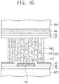
- FIG. 6G is an enlarged cross-sectional view illustrating a second sealing member SS2 according to an embodiment of the invention.
- Planar shapes of the first and second sealing members SS1 and SS2 are illustrated in FIG. 6A .
- At least one of the first sealing member SS1 or the second sealing member SS2 may have a closed line shape (e.g., a closed loop shape) when viewed in a plan view.
- the first sealing member SS1 and the second sealing member SS2 may be spaced apart from each other.
- the first sealing member SS1 may be formed on an outer perimeter of the display panel and the second sealing member SS2 may be formed inside the outer perimeter of the display panel.
- the first sealing member SS1 and the second sealing member SS2 are disposed between the first display substrate 100 and the second display substrate 200 to form the cell gap GP.
- the first and second sealing members SS1 and SS2, each of which has the closed line shape, are illustrated as an example in FIG. 6A .
- the second sealing member SS2 is disposed inside the first sealing member SS1 when viewed in a plan view.
- the second sealing member SS2 may overlap with the voltage supply line DVL illustrated in FIG. 2 .
- the first sealing member SS1 and the second sealing member SS2 are formed in the non-display area NDA.
- the first sealing member SS1 may be disposed along an edge or a perimeter of the display panel DP when viewed in a plan view. In other words, a side surface of the first sealing member SS1 may form a portion of the side surface of the display panel DP.
- the liquid crystal layer LCL (see FIG. 6C ) may be disposed in an inner space of the cell gap GP, which is defined by the second sealing member SS2.
- FIGS. 6B and 6C illustrate one pad area PDA of FIG. 6A in detail.
- an end portion PL-GE of the auxiliary signal line PL-G overlaps with the pad area PDA.
- the end portion PL-GE of the auxiliary signal line PL-G may be a portion of the auxiliary signal line PL-G and may be defined as a portion of the auxiliary signal line PL-G, which overlaps with the first sealing member SS1.
- the end portion PL-GE may be defined as the whole or a part of the portion, overlapping with the first sealing member SS1, of the auxiliary signal line PL-G.
- a side surface PL-GS of the auxiliary signal line PL-G (e.g., a side surface PL-GS of the end portion PL-GE of the auxiliary signal line PL-G) may be substantially aligned with a side surface BSi-S of the first base substrate BS1.
- a side surface SSi-S of the first sealing member SS1 may be substantially aligned with the side surface BSi-S of the first base substrate BS1.
- the side surface BSi-S of the first base substrate BS1 may be substantially aligned with a side surface BS2-S of the second base substrate BS2.
- connection pad CP is disposed on the side surface of the display panel DP.
- the connection pad CP may be coupled to at least the side surface BSi-S of the first base substrate BS1, the side surface SSi-S of the first sealing member SS1 and the side surface BS2-S of the second base substrate BS2.
- a length of the connection pad CP in the third direction DR3 may be adjusted such that the connection pad CP may not be in contact with the side surface BS2-S of the second base substrate BS2.
- connection pad CP is connected to the end portion PL-GE of the auxiliary signal line PL-G.
- the connection pad CP may be provided in plurality, and the connection pads CP may be connected to the side surfaces PL-GS of the end portions PL-GE in one-to-one correspondence.
- the connection pad CP may be electrically connected to a pad GCB-P of the circuit board GCB through an anisotropic conductive film (ACF).
- ACF anisotropic conductive film
- the anisotropic conductive film (ACF) may be replaced with solder paste, and the connection pad CP may be connected directly to the pad GCB-P of the circuit board GCB.
- connection pad CP is disposed on the side surface of the display panel DP
- the circuit board GCB may be connected to the side surface of the display panel DP.
- a connection area of the circuit board GCB and the display panel DP may be defined on the side surface of the display panel DP, and thus an area of the non-display area NDA may be reduced.
- FIGS. 6D and 6E illustrate one non-pad area NPDA of FIG. 6A in detail.
- a signal line e.g., the auxiliary signal line PL-G
- the signal line does not overlap with a portion of the first sealing member SS1, which is disposed in the non-pad area NPDA.
- An end portion of the common electrode CE may overlap with the first sealing member SS1.
- the side surface SSi-S of the first sealing member SS1 may be substantially aligned with the side surface BSi-S of the first base substrate BS1 and the side surface BS2-S of the second base substrate BS2 in each of the non-pad area NPDA and the pad area PDA.
- the first sealing member SS1 may firmly support an edge area of the display panel DP in a plan view.
- the first sealing member SS1 may be a non-conductive sealing member, and the second sealing member SS2 may be a conductive sealing member. As illustrated in FIG. 6F , the first sealing member SS1 may include a first synthetic resin PM1 and first inorganic fillers IP1 mixed with the first synthetic resin PM1. The first inorganic fillers IP1 may improve a hardness of the first sealing member SS1.
- the first synthetic resin PM1 may include an acrylic epoxy-based resin.
- the first inorganic fillers IP1 may include a silica-based inorganic material.
- the first inorganic fillers IP1 may include two different kinds of inorganic fillers.
- the first synthetic resin PM1 may further include other additive(s).
- the additives may include an amine-based hardener and a photo initiator.
- the additives may further include a silane-based additive and an acrylic-based additive.
- the second sealing member SS2 may include a second synthetic resin PM2, second inorganic fillers IP2 mixed with the second synthetic resin PM2, and conductive particles CPS mixed with the second synthetic resin PM2.
- the conductive particles CPS electrically connect the voltage supply line DVL to the common electrode CE.
- the voltage supply line DVL may be disposed on the first insulating layer 10 and may be formed by the same process as the input electrode SE (see FIG. 5A ). Alternatively, the voltage supply line DVL may be disposed on a layer different from the first insulating layer 10.
- the second synthetic resin PM2 may include the same material as the first synthetic resin PM1, and the second inorganic fillers IP2 may include the same material as the first inorganic fillers IP1.
- the conductive particles CPS may include gold particles and/or nickel particles. Diameters (e.g., an average diameter) of the conductive particles CPS may be less than diameters (e.g., an average diameter) of the first inorganic fillers IP1 and diameters (e.g., an average diameter) of the second inorganic fillers IP2.
- a weight % of the second inorganic fillers IP2 with respect to the second sealing member SS2 may be less than a weight % of the first inorganic fillers IP1 with respect to the first sealing member SS1.
- a first mixture and a synthetic resin for the first sealing member SS1 may be mixed with a second mixture including metal particles to form a mixture for the second sealing member SS2.
- the second inorganic fillers IP2 of the second sealing member SS2 may be omitted.
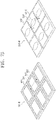
- FIG. 7A is a perspective view illustrating a work display panel DP-W according to an embodiment of the invention.
- FIG. 7B is a perspective view illustrating a first work display substrate 100-W and a second work display substrate 200-W according to an embodiment of the invention.
- FIG. 7C is a cross-sectional view illustrating cell areas CA1 and CA2 of first and second work display substrates 100-W and 200-W according to an embodiment of the invention.
- FIG. 7D is a cross-sectional view illustrating a work display panel DP-W according to an embodiment of the invention.
- FIGS. 7E and 7F are cross-sectional views illustrating a preliminary display panel DP-P according to an embodiment of the invention.
- the same process may be performed on a plurality of cell areas CA defined in the work display panel DP-W to form the display panel DP (see FIGS. 1 to 6G ) in each of the cell areas CA.
- the cell areas CA are divided by a boundary area BA.
- the first work display substrate 100-W and the second work display substrate 200-W are coupled to each other to form the work display panel DP-W.
- the first work display substrate 100-W may include first cell areas CA1 corresponding to the cell areas CA and a first boundary area BA1 corresponding to the boundary area BA.
- the second work display substrate 200-W may include second cell areas CA2 corresponding to the cell areas CA and a second boundary area BA2 corresponding to the boundary area BA.
- the first cell area CA1 may correspond to the first display substrate 100 described with reference to FIGS. 1 to 6G
- the second cell area CA2 may correspond to the second display substrate 200 described with reference to FIGS. 1 to 6G .
- a first sealing member SS1 and a second sealing member SS2 are formed in one of the first cell area CA1 and the second cell area CA2, and a liquid crystal composition LC-C is provided in the other of the first cell area CA1 and the second cell area CA2. At this time, the first sealing member SS1 and the second sealing member SS2 are in an unhardened state.
- the first sealing member SS1 and the second sealing member SS2 may be formed on the first cell area CA1 of the first work display substrate 100-W.
- a height Hi of the first sealing member SS1 may be equal to or greater than a height H2 of the second sealing member SS2.
- a pressure applied to the first sealing member SS1 may be greater than a pressure applied to the second sealing member SS2 when the first work display substrate 100-W is coupled to the second work display substrate 200-W.
- the height Hi of the first sealing member SS1 may be 5% to 20% (in particular, 10% to 20%) greater than the height H2 of the second sealing member SS2.
- the work display panel DP-W may be cut to form preliminary display panels DP-P (see FIG. 7E ).
- a structure extending from structures of the cell areas CA may be disposed in the boundary area BA of the work display panel DP-W.
- the work display panel DP-W may be cut along a cutting line CL illustrated in FIG. 7D by, for example, a scribing process to separate the preliminary display panels DP-P respectively formed in the cell areas CA. Since the first sealing members SS1 of the cell areas CA do not overlap with the cutting line CL, the first sealing members SS1 are not damaged by the cutting process.
- a side surface of the preliminary display panel DP-P of FIG. 7E is in a nonuniform state, as compared with the side surface of the display panel DP of FIG. 6C .
- the side surface of the preliminary display panel DP-P is ground using a grinder GM (a grinding process).
- a side surface of the first display substrate 100, a side surface of the second display substrate 200 and a side surface of the first sealing member SS1 may be substantially aligned with each other by the grinding process, as illustrated in FIG. 7F .
- a cross-sectional shape of the auxiliary signal line PL-G may be changed depending on a grinding method (e.g., a rotational direction of the grinder GM).
- the side surface of the auxiliary signal line PL-G and the side surface of the first base substrate BS1 may be substantially aligned with each other regardless of the grinding method.
- the term “substantial alignment” may include a case in which the side surfaces of the first sealing member SS1, the auxiliary signal line PL-G and the first and second base substrates BS1 and BS2 constitute one surface.
- the term “substantial alignment” may also include variations as a result of manufacturing techniques and/or process tolerances.
- the side surface of the auxiliary signal line PL-G may have a fine curved surface formed by the grinder GM.
- a corner defining the curved side surface of the auxiliary signal line PL-G may be aligned with a corner defining a side surface of an insulating structure.
- the first sealing member SS1 maintains tension between the first display substrate 100 and the second display substrate 200 to prevent the insulating layers 10, 20, 40 and 50 of the first and second display substrates 100 and 200 and/or the auxiliary signal line PL-G from being damaged in the grinding process.
- the first sealing member SS1 supports the first display substrate 100 and the second display substrate 200 to prevent the side surface of the display panel DP from being damaged or deformed by friction of the grinder GM.
- connection pads CP may be formed on the side surface of the display panel DP after the grinding process.
- Metal paste may be printed on the side surface of the display panel DP, and then, a laser patterning process may be performed on the metal paste to form the connection pads CP corresponding to the auxiliary signal lines PL-G, respectively.
- a process of connecting the circuit boards GCB and DCB to the connection pads CP may be performed.
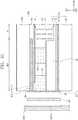
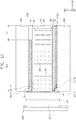
- FIGS. 8 to 15 are cross-sectional views illustrating pad areas PDA according to some embodiments of the invention.
- FIGS. 8 to 15 illustrate cross-sectional views corresponding to FIG. 6C .
- the detailed descriptions to the same components as in the embodiments of FIGS. 1 to 7E will be omitted for the purpose of ease and convenience in description.
- the display panel DP may further include an auxiliary electrode SBE.
- the auxiliary electrode SBE overlaps with the auxiliary signal line PL-G and the first sealing member SS1.
- the auxiliary electrode SBE may be disposed on the first insulating layer 10 and may be formed through the same process as the input electrode SE of FIG. 5A .
- a plurality of the auxiliary electrodes SBE may correspond to the auxiliary signal lines PL-G in one-to-one correspondence or one auxiliary electrode SBE may overlap with a plurality of the auxiliary signal lines PL-G.
- a side surface of the auxiliary electrode SBE may be aligned with the side surface of the first base substrate BS1.
- the connection pad CP may be in contact with the side surface of the auxiliary electrode SBE.
- the auxiliary electrode SBE may be disposed on the auxiliary signal line PL-G to withstand stress applied to the auxiliary signal line PL-G in the grinding process, and thus damage/deformation of the auxiliary signal line PL-G may be prevented.
- the auxiliary electrode SBE may be connected to the end portion PL-GE of the auxiliary signal line PL-G.
- a portion of the first insulating layer 10 may be removed. Removed areas of the first insulating layer 10 may correspond to the auxiliary signal lines PL-G in one-to-one correspondence or one removed area may overlap with a plurality of the auxiliary signal lines PL-G.
- An electrical connection area between the connection pad CP and the auxiliary signal line PL-G may be increased by the auxiliary electrode SBE, and thus a contact resistance between the connection pad CP and the auxiliary signal line PL-G may be reduced.
- the display panel DP may further include a third insulating layer 30 overlapping with the non-display area NDA.
- the third insulating layer 30 may be a color filter 30.
- a color of the color filter 30 may be a red color, a green color, or a blue color.
- the color filter 30 may be formed by the same process as the color filter (e.g., the third insulating layer 30) of the pixel area PXA (see FIG. 5A ).
- the color filter 30 may have a line shape overlapping with the pad areas PDA (see FIG. 6A ) and the non-pad areas NPDA (see FIG. 6A ) when viewed in a plan view. Since the color filter 30 is disposed, heights of the first and second sealing members SS1 and SS2 may be reduced.
- the color filter 30 may overlap with only one of the first and second sealing members SS1 and SS2.
- the height of the one of the first and second sealing members SS1 and SS2 may be reduced.
- a thickness Thi of the end portion PL-GE of the auxiliary signal line PL-G may be greater than a thickness Th2 of an inner portion, not overlapping with the first sealing member SS1, of the auxiliary signal line PL-G. This is because the end portion PL-GE is deformed by the friction of the grinder GM in the grinding process illustrated in FIG. 7E .
- the end portion PL-GE of the auxiliary signal line PL-G may be partially spaced apart from a top surface of the first base substrate BS1. This is because stress is applied to the end portion PL-GE of the auxiliary signal line PL-G by the grinder GM in the grinding process illustrated in FIG. 7E .
- conductive sludge CSG may be disposed between the end portion PL-GE of the auxiliary signal line PL-G and a portion of the top surface of the first base substrate BS1, from which the end portion PL-GE of the auxiliary signal line PL-G is spaced apart.
- the conductive sludge CSG may include a ground material of the auxiliary signal line PL-G and a ground material of the first base substrate BS1.
- the conductive sludge CSG may further include a ground material of the first insulating layer 10.
- connection pad CP may be disposed between the end portion PL-GE of the auxiliary signal line PL-G and the portion of the top surface of the first base substrate BS1, from which the end portion PL-GE of the auxiliary signal line PL-G is spaced apart.
- the conductive paste may be inserted into a space between the end portion PL-GE and the first base substrate BS1 in the process of printing the conductive paste.
- the first sealing member SS1 and the second sealing member SS2 may be in contact with each other.
- a distance between the first and second sealing members SS1 and SS2 is designed to be narrow in the process of forming the first and second sealing members SS1 and SS2 in FIG. 7C
- shapes of the first and second sealing members SS1 and SS2 may be deformed in the process of coupling the first work display substrate 100-W to the second work display substrate 200-W.
- the first and second sealing members SS1 and SS2 may be in contact with each other.
- the common electrode CE may not be disposed between the first sealing member SS1 and an insulating layer (e.g., the fifth insulating layer 50) of the second display substrate 200.
- An edge of the common electrode CE may be disposed inside the first sealing member SS1 in a plan view and may not overlap with the first sealing member SS1.
- FIGS. 16A and 16B are plan views illustrating display panels DP according to some embodiments of the invention.
- FIGS. 16A and 16B illustrate plan views corresponding to FIG. 6A .
- a second sealing member may include a plurality of portions SS2-P spaced apart from each other. At least one of the portions SS2-P may have the same cross-sectional shape as illustrated in FIG. 6G . That is, the second sealing member does not have to form a closed loop but can be formed by portions SS2-P to form a loop around a perimeter of the display panel inside the outer perimeter of the display panel. Meanwhile, the first sealing member SS1 may form a closed perimeter around the display panel.
- a first sealing member may include a plurality of portions SS1-P spaced apart from each other.
- the portions SS1-P may overlap with at least the non-pad areas NPDA. That is, the first sealing member does not have to form a closed loop but can be formed by portions SS1-P to form a loop around the outer perimeter of the display panel. Meanwhile, the second sealing member SS2 may form a closed perimeter around the display panel.
- Embodiments of the invention can provide a display panel comprising: a first display substrate; a second display substrate facing and spaced apart from the first display substrate; a non-conductive sealing member disposed between the first display substrate and the second display substrate; a conductive sealing member disposed between the first display substrate and the second display substrate and disposed inside the non-conductive sealing member when viewed in a plan view; and a connection pad coupled to a side surface of the first display substrate and a side surface of the non-conductive sealing member, wherein the first display substrate comprises: a first base substrate; a thin film transistor disposed over the first base substrate; at least one insulating layer disposed over the first base substrate; a pixel electrode disposed over the first base substrate and connected to the thin film transistor; a signal line disposed on the first base substrate and including an end portion overlapping with the non-conductive sealing member and connected to the connection pad; and a voltage supply line disposed over the first base substrate and connected to the conductive sealing member.
- the conductive sealing member may surround a display area of the display panel, and the non-conductive sealing member may be spaced apart from and surround the conductive sealing member.
- the second display substrate comprises a second base substrate and a common electrode disposed over one surface of the second base substrate.
- the conductive sealing member is electrically connected to the common electrode.
- the display panel may comprise a plurality of signal lines and connection pads, each said signal line being disposed on the first base substrate and including an end portion overlapping with the non-conductive sealing member and connected to a connection pad.
- the signal lines may be, for example, respectively connected to a gate line or a data line of the display panel.
- the signal line may be disposed over a top surface of the first base substrate, wherein the signal line includes: an end portion overlapping with the non-conductive sealing member and connected to the connection pad.
- the display panel may further comprise an auxiliary electrode connected to the end portion of the signal line and the connection pad.
- the second display substrate may comprise: a second base substrate; and a common electrode disposed on a bottom surface of the second base substrate and overlapping with the non-conductive sealing member.
- Embodiments of the invention provide a display panel according to claim 1 and inter alia comprising: a first display substrate; a second display substrate facing and spaced apart from the first display substrate; a non-conductive sealing member disposed between the first display substrate and the second display substrate; and a connection pad coupled to a side surface of the first display substrate and a side surface of the non-conductive sealing member
- the first display substrate comprises: a first base substrate including a side surface substantially aligned with the side surface of the non-conductive sealing member; a signal line disposed over a top surface of the first base substrate, wherein the signal line includes: an end portion overlapping with the non-conductive sealing member and connected to the connection pad; and an auxiliary electrode connected to the end portion of the signal line and the connection pad
- the second display substrate comprises: a second base substrate; and a common electrode disposed on a bottom surface of the second base substrate and overlapping with the non-conductive sealing member.
- Embodiments of the invention provide a method of fabricating a display panel, the method being according to claim 14 and inter alia comprising: providing a first work display substrate including:
- connection pad may is on the side surface of the display panel, and thus the circuit board may be connected to the side surface of the display panel. Since a connection area of the circuit board and the display panel is defined on the side surface of the display panel, an area of the non-display area may be reduced.
- the non-conductive sealing member is disposed outside the conductive sealing member in a plan view, and thus an edge area of the first and second display substrates may be firmly supported by the non-conductive sealing member.
- the non-conductive sealing member may maintain tension between the first and second display substrates to prevent the insulating layers of the first and second display substrates and/or the signal line from being damaged in a fabrication process (e.g., the grinding process).
- a contact area defined on the side surface of the signal line may be secured to reduce a contact resistance between the circuit board and the display panel.
Landscapes
- Physics & Mathematics (AREA)
- Nonlinear Science (AREA)
- Optics & Photonics (AREA)
- Crystallography & Structural Chemistry (AREA)
- Chemical & Material Sciences (AREA)
- General Physics & Mathematics (AREA)
- Mathematical Physics (AREA)
- Engineering & Computer Science (AREA)
- Microelectronics & Electronic Packaging (AREA)
- Devices For Indicating Variable Information By Combining Individual Elements (AREA)
- Manufacturing & Machinery (AREA)
- Geometry (AREA)
- Electroluminescent Light Sources (AREA)
Claims (14)
- Anzeigetafel, umfassend:ein erstes Anzeigesubstrat (100);ein zweites Anzeigesubstrat (200), das dem ersten Anzeigesubstrat (100) zugewandt und von diesem beabstandet ist;wobei das zweite Anzeigesubstrat (200) ein zweites Basissubstrat (BS-2) umfasst;ein nichtleitendes Dichtungselement (SS1), das zwischen dem ersten Anzeigesubstrat (100) und dem zweiten Anzeigesubstrat (200) angeordnet ist; undein Anschlusspad (CP), das mit einer Seitenfläche des ersten Anzeigesubstrats (100) und einer Seitenfläche des nichtleitenden Dichtungselements (SS1) gekoppelt ist,wobei das erste Anzeigesubstrat (100) Folgendes umfasst:ein erstes Basissubstrat (BS-1);einen Dünnfilmtransistor (TR), der über dem ersten Basissubstrat (BS-1) angeordnet ist;mindestens eine Isolationsschicht (10, 20, 40), die über dem ersten Basissubstrat (BS-1) angeordnet ist;eine Pixelelektrode (PE), die über dem ersten Basissubstrat (BS-1) angeordnet und mit dem Dünnfilmtransistor verbunden ist;eine Signalleitung (PL-G), die über dem ersten Basissubstrat (BS-1) angeordnet ist und einen Endabschnitt (PL-GE) aufweist, der mit dem nichtleitenden Dichtungselement (SS1) überlappt und mit dem Anschlusspad (CP) verbunden ist; unddadurch gekennzeichnet, dass die Anzeigetafel ferner Folgendes aufweist:ein leitendes Dichtungselement (SS2), das zwischen dem ersten Anzeigesubstrat (100) unddem zweiten Anzeigesubstrat angeordnet ist und innerhalb des durch das nichtleitende Dichtungselement (SS1) definierten Bereichs in einer Draufsicht bei Betrachtung in einer Richtung senkrecht zu den Anzeigesubstraten angeordnet ist;
eine Spannungsversorgungsleitung (DVL), die über dem ersten Basissubstrat (BS-1) angeordnet und mit dem leitenden Dichtungselement (SS2) verbunden ist, wobei das zweite Anzeigesubstrat (200) Folgendes umfasst:
eine gemeinsame Elektrode (CE), die über einer Oberfläche des zweiten Basissubstrats angeordnet ist,wobei das leitende Dichtungselement (SS2) die gemeinsame Elektrode (CE) und die Spannungsversorgungsleitung (DVL) elektrisch verbindet. - Anzeigetafel nach Anspruch 1, wobei das nichtleitende Dichtungselement (SS1) Folgendes umfasst:ein erstes Kunstharz; underste anorganische Füllstoffe, die mit dem ersten Kunstharz gemischt sind.
- Anzeigetafel nach Anspruch 2, wobei das leitende Dichtungselement (SS2) Folgendes umfasst:ein zweites Kunstharz; undleitende Partikel, die mit dem zweiten Kunstharz gemischt sind;wobei das leitende Dichtungselement (SS2) optional ferner zweite anorganische Füllstoffe umfasst, die mit dem zweiten Kunstharz gemischt sind;wobei ein Durchmesser der leitenden Partikel optional kleiner als ein Durchmesser der ersten anorganischen Füllstoffe ist.
- Anzeigetafel nach einem der Ansprüche 1 bis 3, wobei die Seitenfläche des nichtleitenden Dichtungselements (SS1) im Wesentlichen mit einer Seitenfläche des ersten Basissubstrats (BS-1) ausgerichtet ist.
- Anzeigetafel nach einem der Ansprüche 1 bis 4, wobei eine Seitenfläche des Endabschnitts der Signalleitung im Wesentlichen mit einer Seitenfläche des ersten Basissubstrats (BS-1) ausgerichtet ist.
- Anzeigetafel nach einem der Ansprüche 1 bis 5, wobei das nichtleitende Dichtungselement (SS1) mit der gemeinsamen Elektrode verbunden ist.
- Anzeigetafel nach einem der Ansprüche 1 bis 6, wobei der Dünnfilmtransistor eine Steuerelektrode, einen aktiven Teil sowie eine Eingangselektrode und eine Ausgangselektrode, die auf einer Schicht angeordnet sind, die sich von einer Schicht unterscheidet, auf der die Steuerelektrode angeordnet ist, umfasst, und
wobei die Spannungsversorgungsleitung auf der gleichen Schicht wie die Steuerelektrode oder die Eingangselektrode angeordnet ist. - Anzeigetafel nach Anspruch 7, ferner umfassend:eine Hilfselektrode, die mit dem Endabschnitt (PL-GE) der Signalleitung (PL-G) überlappt,
und wobei die Signalleitung (PL-G) auf der gleichen Schicht wie die Steuerelektrode angeordnet ist,wobei die Hilfselektrode optional auf derselben Schicht wie die Eingangselektrode angeordnet ist;wobei die Hilfselektrode optional mit dem Endabschnitt der Signalleitung (PL-G) verbunden ist. - Anzeigetafel nach einem der Ansprüche 1 bis 8, wobei die Isolationsschicht eine Mehrzahl von Farbfiltern umfasst, und
wobei einer aus der Mehrzahl von Farbfiltern mit der Pixelelektrode (PE) überlappt,
wobei die Isolationsschicht optional ferner eine erste anorganische Schicht, die unter der Mehrzahl von Farbfiltern angeordnet ist, und eine zweite anorganische Schicht, die auf der Mehrzahl von Farbfiltern angeordnet ist, umfasst. - Anzeigetafel nach Anspruch 9, wobei ein anderer aus der Mehrzahl von Farbfiltern mit mindestens einem der nichtleitenden Dichtungselemente (SS1) oder dem leitenden Dichtungselement (SS2) überlappt.
- Anzeigetafel nach einem der Ansprüche 1 bis 10, wobei eine Dicke des Endabschnitts (PL-GE) der Signalleitung (PL-G) größer ist als eine Dicke der Signalleitung (PL-G), die nicht mit dem nichtleitenden Dichtungselement (SS1) überlappt.
- Anzeigetafel nach einem der Ansprüche 1 bis 11, wobei der Endabschnitt (PL-GE) der Signalleitung (PL-G) von einer oberen Fläche des ersten Basissubstrats (BS-1) beabstandet ist;
wobei leitender Schlamm optional zwischen dem Endabschnitt (PL-GE) der Signalleitung (PL-G) und einem Abschnitt der oberen Oberfläche des ersten Basissubstrats (BS-1) angeordnet ist, von dem der Endabschnitt (PL-GE) der Signalleitung (PL-G) beabstandet ist, angeordnet ist. - Anzeigetafel nach einem der Ansprüche 1 bis 12, wobei mindestens eines der nichtleitenden Dichtungselemente (SS1) oder das leitende Dichtungselement (SS2) in einer Draufsicht einen geschlossenen Umfang um die Anzeigetafel bildet.
- Verfahren zur Herstellung der Anzeigetafel nach einem der Ansprüche 1 bis 13, wobei das Verfahren Folgendes umfasst:Bereitstellen eines Anzeigesubstrats für ein erstes Werkstück, das Folgendes umfasst: erste Zellbereiche; und einen ersten Grenzbereich, der die ersten Zellbereiche unterteilt;Bereitstellen eines Anzeigesubstrats für ein zweites Werkstück, das Folgendes umfasst: zweite Zellbereiche, die den ersten Zellbereichen entsprechen; und einen zweiten Grenzbereich, der dem ersten Grenzbereich entspricht;Ausbilden eines nichtleitenden Dichtungselements mit einer ersten Höhe und ein leitendes Dichtungselement mit einer zweiten Höhe, die geringer ist als die erste Höhe, in jedem der ersten Zellbereiche, wobei das leitende Dichtungselement in Draufsicht gesehen innerhalb des nichtleitenden Dichtungselements angeordnet ist;Bereitstellen eines Flüssigkristallmaterials für jeden der zweiten Zellbereiche; Koppeln des Anzeigesubstrats für ein erstes Werkstück und des Anzeigesubstrats für ein zweites Werkstück zum Bilden einer Werkstückanzeigetafel;Schneiden der Werkstückanzeigetafel entlang des ersten Grenzbereichs, um eine vorläufige Anzeigetafel von der Werkstückanzeigetafel zu trennen;Schleifen einer Seitenfläche der vorläufigen Anzeigetafel; und Ausbilden eines Anschlusspads auf der Seitenfläche der vorläufigen Anzeigetafel.
Applications Claiming Priority (1)
| Application Number | Priority Date | Filing Date | Title |
|---|---|---|---|
| KR1020180000385A KR20190083027A (ko) | 2018-01-02 | 2018-01-02 | 표시패널 및 그 제조방법 |
Publications (3)
| Publication Number | Publication Date |
|---|---|
| EP3506004A2 EP3506004A2 (de) | 2019-07-03 |
| EP3506004A3 EP3506004A3 (de) | 2019-08-14 |
| EP3506004B1 true EP3506004B1 (de) | 2020-09-16 |
Family
ID=64901890
Family Applications (1)
| Application Number | Title | Priority Date | Filing Date |
|---|---|---|---|
| EP18215627.3A Active EP3506004B1 (de) | 2018-01-02 | 2018-12-21 | Anzeigetafel und verfahren zur herstellung davon |
Country Status (4)
| Country | Link |
|---|---|
| US (2) | US10634955B2 (de) |
| EP (1) | EP3506004B1 (de) |
| KR (1) | KR20190083027A (de) |
| CN (1) | CN109991784A (de) |
Families Citing this family (16)
| Publication number | Priority date | Publication date | Assignee | Title |
|---|---|---|---|---|
| KR20190083027A (ko) * | 2018-01-02 | 2019-07-11 | 삼성디스플레이 주식회사 | 표시패널 및 그 제조방법 |
| KR102839408B1 (ko) | 2019-01-17 | 2025-07-28 | 삼성디스플레이 주식회사 | 표시 장치 및 이의 제조 방법 |
| JP6835122B2 (ja) * | 2019-03-20 | 2021-02-24 | セイコーエプソン株式会社 | 電気光学装置および電子機器 |
| KR102939374B1 (ko) * | 2019-06-28 | 2026-03-17 | 삼성디스플레이 주식회사 | 표시 장치 및 그 제조 방법 |
| KR102741459B1 (ko) * | 2019-08-07 | 2024-12-12 | 삼성디스플레이 주식회사 | 표시모듈, 표시모듈 검사장치, 및 표시모듈 검사방법 |
| KR20210024345A (ko) * | 2019-08-22 | 2021-03-05 | 삼성디스플레이 주식회사 | 표시 장치 |
| KR20210027666A (ko) * | 2019-08-30 | 2021-03-11 | 삼성디스플레이 주식회사 | 표시 장치 및 그 제조 방법 |
| KR102794821B1 (ko) * | 2019-09-02 | 2025-04-11 | 삼성디스플레이 주식회사 | 표시 장치의 제조 방법, 및 표시 장치의 제조 장치 |
| KR102807945B1 (ko) * | 2019-09-02 | 2025-05-15 | 삼성디스플레이 주식회사 | 표시 장치 |
| KR102903685B1 (ko) * | 2019-09-04 | 2025-12-24 | 삼성디스플레이 주식회사 | 표시 장치 |
| KR20210037035A (ko) * | 2019-09-26 | 2021-04-06 | 삼성디스플레이 주식회사 | 표시기판, 이를 포함하는 표시장치 및 표시기판의 제조방법 |
| CN110989234A (zh) * | 2019-12-23 | 2020-04-10 | 惠州市华星光电技术有限公司 | 显示面板及其制备方法、显示装置 |
| JP7522650B2 (ja) * | 2020-12-18 | 2024-07-25 | 上海天馬微電子有限公司 | 曲面液晶パネル及び曲面液晶パネルの製造方法 |
| US11515271B2 (en) | 2021-01-27 | 2022-11-29 | Innolux Corporation | Electronic device including wire on side surface of substrate and manufacturing method thereof |
| CN113589596B (zh) * | 2021-07-16 | 2023-01-10 | 惠州华星光电显示有限公司 | 显示面板及其制备方法 |
| KR20230139825A (ko) * | 2022-03-22 | 2023-10-06 | 삼성디스플레이 주식회사 | 회로기판 및 이를 포함하는 표시 장치 |
Family Cites Families (29)
| Publication number | Priority date | Publication date | Assignee | Title |
|---|---|---|---|---|
| EP3716257B1 (de) * | 2001-09-07 | 2021-01-20 | Joled Inc. | El-anzeigetafel, verfahren zur ansteuerung davon und el-anzeigevorrichtung |
| JP2004212955A (ja) * | 2002-12-16 | 2004-07-29 | Sharp Corp | 液晶表示装置 |
| US7385651B2 (en) * | 2002-12-26 | 2008-06-10 | Lg Display Co., Ltd. | Array substrate for liquid crystal display device and method of manufacturing the same |
| TWI221942B (en) | 2003-08-21 | 2004-10-11 | Toppoly Optoelectronics Corp | Liquid crystal display device |
| TW200710471A (en) * | 2005-07-20 | 2007-03-16 | Samsung Electronics Co Ltd | Array substrate for display device |
| JP5306784B2 (ja) * | 2008-11-18 | 2013-10-02 | 株式会社ジャパンディスプレイ | 表示装置 |
| KR101804554B1 (ko) * | 2010-11-01 | 2017-12-05 | 삼성디스플레이 주식회사 | 표시 장치 및 유기 발광 표시 장치 |
| KR101839954B1 (ko) * | 2010-12-17 | 2018-03-20 | 삼성디스플레이 주식회사 | 표시 장치 및 유기 발광 표시 장치 |
| JP5756693B2 (ja) * | 2011-07-06 | 2015-07-29 | 積水化学工業株式会社 | 液晶滴下工法用シール剤、上下導通材料、及び、液晶表示素子 |
| KR101484022B1 (ko) * | 2012-05-31 | 2015-01-19 | 엘지디스플레이 주식회사 | 액정표시장치용 어레이 기판 및 이의 제조 방법 |
| US9625764B2 (en) * | 2012-08-28 | 2017-04-18 | Semiconductor Energy Laboratory Co., Ltd. | Display device and electronic device |
| KR101982095B1 (ko) | 2012-10-17 | 2019-05-24 | 엘지디스플레이 주식회사 | 씰 패턴을 구비한 액정표시장치 |
| US8994042B2 (en) * | 2013-05-20 | 2015-03-31 | Lg Electronics Inc. | Display panel and display device |
| KR102230752B1 (ko) * | 2013-12-20 | 2021-03-19 | 엘지디스플레이 주식회사 | 표시장치 및 표시장치의 제조방법 |
| KR102185756B1 (ko) * | 2014-03-31 | 2020-12-03 | 삼성디스플레이 주식회사 | 표시 기판 및 이를 포함하는 액정 표시 장치 |
| KR20250028505A (ko) * | 2014-09-12 | 2025-02-28 | 가부시키가이샤 한도오따이 에네루기 켄큐쇼 | 표시 장치 |
| US10310341B2 (en) | 2015-06-29 | 2019-06-04 | Lg Display Co., Ltd. | Display device and method of manufacturing the same |
| KR102584326B1 (ko) * | 2015-06-29 | 2023-10-04 | 엘지디스플레이 주식회사 | 디스플레이 장치 및 그 제조 방법 |
| KR102417804B1 (ko) * | 2015-07-01 | 2022-07-06 | 엘지디스플레이 주식회사 | 디스플레이 장치 |
| KR102387880B1 (ko) * | 2015-07-03 | 2022-04-18 | 엘지디스플레이 주식회사 | 디스플레이 장치 |
| JP6560556B2 (ja) * | 2015-07-16 | 2019-08-14 | 株式会社ジャパンディスプレイ | 表示装置 |
| KR102378891B1 (ko) * | 2015-09-18 | 2022-03-24 | 엘지디스플레이 주식회사 | 디스플레이 패널 및 이를 포함하는 디스플레이 장치 |
| CN105655349B (zh) * | 2016-01-05 | 2019-08-20 | 京东方科技集团股份有限公司 | 阵列基板及其制作方法、显示面板、显示装置 |
| KR102535145B1 (ko) * | 2016-06-13 | 2023-05-22 | 삼성디스플레이 주식회사 | 표시 장치 |
| KR102413716B1 (ko) | 2017-09-25 | 2022-06-28 | 삼성디스플레이 주식회사 | 표시패널 |
| KR20190083027A (ko) * | 2018-01-02 | 2019-07-11 | 삼성디스플레이 주식회사 | 표시패널 및 그 제조방법 |
| JP6946220B2 (ja) * | 2018-03-26 | 2021-10-06 | 株式会社ジャパンディスプレイ | 表示装置 |
| KR102617812B1 (ko) * | 2018-05-10 | 2023-12-27 | 삼성디스플레이 주식회사 | 유기발광 표시 장치 |
| US20200166792A1 (en) * | 2018-11-26 | 2020-05-28 | HKC Corporation Limited | Array substrate, manufacturing method of the array substrate, and display device |
-
2018
- 2018-01-02 KR KR1020180000385A patent/KR20190083027A/ko not_active Ceased
- 2018-12-21 EP EP18215627.3A patent/EP3506004B1/de active Active
- 2018-12-25 CN CN201811588050.0A patent/CN109991784A/zh active Pending
- 2018-12-31 US US16/236,648 patent/US10634955B2/en active Active
-
2020
- 2020-03-11 US US16/816,144 patent/US11143917B2/en active Active
Non-Patent Citations (1)
| Title |
|---|
| None * |
Also Published As
| Publication number | Publication date |
|---|---|
| US10634955B2 (en) | 2020-04-28 |
| US11143917B2 (en) | 2021-10-12 |
| US20190204638A1 (en) | 2019-07-04 |
| EP3506004A2 (de) | 2019-07-03 |
| EP3506004A3 (de) | 2019-08-14 |
| US20200209660A1 (en) | 2020-07-02 |
| CN109991784A (zh) | 2019-07-09 |
| KR20190083027A (ko) | 2019-07-11 |
Similar Documents
| Publication | Publication Date | Title |
|---|---|---|
| EP3506004B1 (de) | Anzeigetafel und verfahren zur herstellung davon | |
| US11686981B2 (en) | Display panel | |
| US11448928B2 (en) | Display panel and method of manufacturing the same | |
| CN110874982B (zh) | 显示设备 | |
| US11747686B2 (en) | Display device and manufacturing method thereof | |
| US12127453B2 (en) | Display device having reduced non-display area | |
| JP2018049193A (ja) | 表示装置 | |
| US11573468B2 (en) | Display substrate including a multi-layer structure of an organic layer and an inorganic layer, display device having the same, and method of manufacturing the display substrate | |
| KR102927492B1 (ko) | 표시장치 |
Legal Events
| Date | Code | Title | Description |
|---|---|---|---|
| PUAI | Public reference made under article 153(3) epc to a published international application that has entered the european phase |
Free format text: ORIGINAL CODE: 0009012 |
|
| STAA | Information on the status of an ep patent application or granted ep patent |
Free format text: STATUS: THE APPLICATION HAS BEEN PUBLISHED |
|
| AK | Designated contracting states |
Kind code of ref document: A2 Designated state(s): AL AT BE BG CH CY CZ DE DK EE ES FI FR GB GR HR HU IE IS IT LI LT LU LV MC MK MT NL NO PL PT RO RS SE SI SK SM TR |
|
| AX | Request for extension of the european patent |
Extension state: BA ME |
|
| PUAL | Search report despatched |
Free format text: ORIGINAL CODE: 0009013 |
|
| AK | Designated contracting states |
Kind code of ref document: A3 Designated state(s): AL AT BE BG CH CY CZ DE DK EE ES FI FR GB GR HR HU IE IS IT LI LT LU LV MC MK MT NL NO PL PT RO RS SE SI SK SM TR |
|
| AX | Request for extension of the european patent |
Extension state: BA ME |
|
| RIC1 | Information provided on ipc code assigned before grant |
Ipc: G02F 1/1345 20060101ALI20190710BHEP Ipc: G02F 1/1339 20060101AFI20190710BHEP |
|
| STAA | Information on the status of an ep patent application or granted ep patent |
Free format text: STATUS: REQUEST FOR EXAMINATION WAS MADE |
|
| 17P | Request for examination filed |
Effective date: 20200213 |
|
| RBV | Designated contracting states (corrected) |
Designated state(s): AL AT BE BG CH CY CZ DE DK EE ES FI FR GB GR HR HU IE IS IT LI LT LU LV MC MK MT NL NO PL PT RO RS SE SI SK SM TR |
|
| GRAP | Despatch of communication of intention to grant a patent |
Free format text: ORIGINAL CODE: EPIDOSNIGR1 |
|
| STAA | Information on the status of an ep patent application or granted ep patent |
Free format text: STATUS: GRANT OF PATENT IS INTENDED |
|
| INTG | Intention to grant announced |
Effective date: 20200403 |
|
| RIN1 | Information on inventor provided before grant (corrected) |
Inventor name: PARK, SAERON Inventor name: SONG, SEUNGKI |
|
| GRAS | Grant fee paid |
Free format text: ORIGINAL CODE: EPIDOSNIGR3 |
|
| GRAA | (expected) grant |
Free format text: ORIGINAL CODE: 0009210 |
|
| STAA | Information on the status of an ep patent application or granted ep patent |
Free format text: STATUS: THE PATENT HAS BEEN GRANTED |
|
| AK | Designated contracting states |
Kind code of ref document: B1 Designated state(s): AL AT BE BG CH CY CZ DE DK EE ES FI FR GB GR HR HU IE IS IT LI LT LU LV MC MK MT NL NO PL PT RO RS SE SI SK SM TR |
|
| REG | Reference to a national code |
Ref country code: GB Ref legal event code: FG4D |
|
| REG | Reference to a national code |
Ref country code: CH Ref legal event code: EP |
|
| REG | Reference to a national code |
Ref country code: DE Ref legal event code: R096 Ref document number: 602018007895 Country of ref document: DE |
|
| REG | Reference to a national code |
Ref country code: IE Ref legal event code: FG4D |
|
| REG | Reference to a national code |
Ref country code: AT Ref legal event code: REF Ref document number: 1314686 Country of ref document: AT Kind code of ref document: T Effective date: 20201015 |
|
| PG25 | Lapsed in a contracting state [announced via postgrant information from national office to epo] |
Ref country code: FI Free format text: LAPSE BECAUSE OF FAILURE TO SUBMIT A TRANSLATION OF THE DESCRIPTION OR TO PAY THE FEE WITHIN THE PRESCRIBED TIME-LIMIT Effective date: 20200916 Ref country code: GR Free format text: LAPSE BECAUSE OF FAILURE TO SUBMIT A TRANSLATION OF THE DESCRIPTION OR TO PAY THE FEE WITHIN THE PRESCRIBED TIME-LIMIT Effective date: 20201217 Ref country code: NO Free format text: LAPSE BECAUSE OF FAILURE TO SUBMIT A TRANSLATION OF THE DESCRIPTION OR TO PAY THE FEE WITHIN THE PRESCRIBED TIME-LIMIT Effective date: 20201216 Ref country code: SE Free format text: LAPSE BECAUSE OF FAILURE TO SUBMIT A TRANSLATION OF THE DESCRIPTION OR TO PAY THE FEE WITHIN THE PRESCRIBED TIME-LIMIT Effective date: 20200916 Ref country code: HR Free format text: LAPSE BECAUSE OF FAILURE TO SUBMIT A TRANSLATION OF THE DESCRIPTION OR TO PAY THE FEE WITHIN THE PRESCRIBED TIME-LIMIT Effective date: 20200916 Ref country code: BG Free format text: LAPSE BECAUSE OF FAILURE TO SUBMIT A TRANSLATION OF THE DESCRIPTION OR TO PAY THE FEE WITHIN THE PRESCRIBED TIME-LIMIT Effective date: 20201216 |
|
| REG | Reference to a national code |
Ref country code: AT Ref legal event code: MK05 Ref document number: 1314686 Country of ref document: AT Kind code of ref document: T Effective date: 20200916 |
|
| REG | Reference to a national code |
Ref country code: NL Ref legal event code: MP Effective date: 20200916 |
|
| PG25 | Lapsed in a contracting state [announced via postgrant information from national office to epo] |
Ref country code: LV Free format text: LAPSE BECAUSE OF FAILURE TO SUBMIT A TRANSLATION OF THE DESCRIPTION OR TO PAY THE FEE WITHIN THE PRESCRIBED TIME-LIMIT Effective date: 20200916 Ref country code: RS Free format text: LAPSE BECAUSE OF FAILURE TO SUBMIT A TRANSLATION OF THE DESCRIPTION OR TO PAY THE FEE WITHIN THE PRESCRIBED TIME-LIMIT Effective date: 20200916 |
|
| REG | Reference to a national code |
Ref country code: LT Ref legal event code: MG4D |
|
| PG25 | Lapsed in a contracting state [announced via postgrant information from national office to epo] |
Ref country code: SM Free format text: LAPSE BECAUSE OF FAILURE TO SUBMIT A TRANSLATION OF THE DESCRIPTION OR TO PAY THE FEE WITHIN THE PRESCRIBED TIME-LIMIT Effective date: 20200916 Ref country code: LT Free format text: LAPSE BECAUSE OF FAILURE TO SUBMIT A TRANSLATION OF THE DESCRIPTION OR TO PAY THE FEE WITHIN THE PRESCRIBED TIME-LIMIT Effective date: 20200916 Ref country code: EE Free format text: LAPSE BECAUSE OF FAILURE TO SUBMIT A TRANSLATION OF THE DESCRIPTION OR TO PAY THE FEE WITHIN THE PRESCRIBED TIME-LIMIT Effective date: 20200916 Ref country code: RO Free format text: LAPSE BECAUSE OF FAILURE TO SUBMIT A TRANSLATION OF THE DESCRIPTION OR TO PAY THE FEE WITHIN THE PRESCRIBED TIME-LIMIT Effective date: 20200916 Ref country code: PT Free format text: LAPSE BECAUSE OF FAILURE TO SUBMIT A TRANSLATION OF THE DESCRIPTION OR TO PAY THE FEE WITHIN THE PRESCRIBED TIME-LIMIT Effective date: 20210118 Ref country code: CZ Free format text: LAPSE BECAUSE OF FAILURE TO SUBMIT A TRANSLATION OF THE DESCRIPTION OR TO PAY THE FEE WITHIN THE PRESCRIBED TIME-LIMIT Effective date: 20200916 |
|
| PG25 | Lapsed in a contracting state [announced via postgrant information from national office to epo] |
Ref country code: AT Free format text: LAPSE BECAUSE OF FAILURE TO SUBMIT A TRANSLATION OF THE DESCRIPTION OR TO PAY THE FEE WITHIN THE PRESCRIBED TIME-LIMIT Effective date: 20200916 Ref country code: AL Free format text: LAPSE BECAUSE OF FAILURE TO SUBMIT A TRANSLATION OF THE DESCRIPTION OR TO PAY THE FEE WITHIN THE PRESCRIBED TIME-LIMIT Effective date: 20200916 Ref country code: ES Free format text: LAPSE BECAUSE OF FAILURE TO SUBMIT A TRANSLATION OF THE DESCRIPTION OR TO PAY THE FEE WITHIN THE PRESCRIBED TIME-LIMIT Effective date: 20200916 Ref country code: IS Free format text: LAPSE BECAUSE OF FAILURE TO SUBMIT A TRANSLATION OF THE DESCRIPTION OR TO PAY THE FEE WITHIN THE PRESCRIBED TIME-LIMIT Effective date: 20210116 Ref country code: PL Free format text: LAPSE BECAUSE OF FAILURE TO SUBMIT A TRANSLATION OF THE DESCRIPTION OR TO PAY THE FEE WITHIN THE PRESCRIBED TIME-LIMIT Effective date: 20200916 |
|
| REG | Reference to a national code |
Ref country code: DE Ref legal event code: R097 Ref document number: 602018007895 Country of ref document: DE |
|
| PG25 | Lapsed in a contracting state [announced via postgrant information from national office to epo] |
Ref country code: SK Free format text: LAPSE BECAUSE OF FAILURE TO SUBMIT A TRANSLATION OF THE DESCRIPTION OR TO PAY THE FEE WITHIN THE PRESCRIBED TIME-LIMIT Effective date: 20200916 |
|
| PLBE | No opposition filed within time limit |
Free format text: ORIGINAL CODE: 0009261 |
|
| STAA | Information on the status of an ep patent application or granted ep patent |
Free format text: STATUS: NO OPPOSITION FILED WITHIN TIME LIMIT |
|
| 26N | No opposition filed |
Effective date: 20210617 |
|
| PG25 | Lapsed in a contracting state [announced via postgrant information from national office to epo] |
Ref country code: SI Free format text: LAPSE BECAUSE OF FAILURE TO SUBMIT A TRANSLATION OF THE DESCRIPTION OR TO PAY THE FEE WITHIN THE PRESCRIBED TIME-LIMIT Effective date: 20200916 Ref country code: DK Free format text: LAPSE BECAUSE OF FAILURE TO SUBMIT A TRANSLATION OF THE DESCRIPTION OR TO PAY THE FEE WITHIN THE PRESCRIBED TIME-LIMIT Effective date: 20200916 Ref country code: MC Free format text: LAPSE BECAUSE OF FAILURE TO SUBMIT A TRANSLATION OF THE DESCRIPTION OR TO PAY THE FEE WITHIN THE PRESCRIBED TIME-LIMIT Effective date: 20200916 |
|
| REG | Reference to a national code |
Ref country code: BE Ref legal event code: MM Effective date: 20201231 |
|
| PG25 | Lapsed in a contracting state [announced via postgrant information from national office to epo] |
Ref country code: IE Free format text: LAPSE BECAUSE OF NON-PAYMENT OF DUE FEES Effective date: 20201221 Ref country code: LU Free format text: LAPSE BECAUSE OF NON-PAYMENT OF DUE FEES Effective date: 20201221 Ref country code: IT Free format text: LAPSE BECAUSE OF FAILURE TO SUBMIT A TRANSLATION OF THE DESCRIPTION OR TO PAY THE FEE WITHIN THE PRESCRIBED TIME-LIMIT Effective date: 20200916 |
|
| PG25 | Lapsed in a contracting state [announced via postgrant information from national office to epo] |
Ref country code: TR Free format text: LAPSE BECAUSE OF FAILURE TO SUBMIT A TRANSLATION OF THE DESCRIPTION OR TO PAY THE FEE WITHIN THE PRESCRIBED TIME-LIMIT Effective date: 20200916 Ref country code: MT Free format text: LAPSE BECAUSE OF FAILURE TO SUBMIT A TRANSLATION OF THE DESCRIPTION OR TO PAY THE FEE WITHIN THE PRESCRIBED TIME-LIMIT Effective date: 20200916 Ref country code: CY Free format text: LAPSE BECAUSE OF FAILURE TO SUBMIT A TRANSLATION OF THE DESCRIPTION OR TO PAY THE FEE WITHIN THE PRESCRIBED TIME-LIMIT Effective date: 20200916 |
|
| PG25 | Lapsed in a contracting state [announced via postgrant information from national office to epo] |
Ref country code: MK Free format text: LAPSE BECAUSE OF FAILURE TO SUBMIT A TRANSLATION OF THE DESCRIPTION OR TO PAY THE FEE WITHIN THE PRESCRIBED TIME-LIMIT Effective date: 20200916 |
|
| PG25 | Lapsed in a contracting state [announced via postgrant information from national office to epo] |
Ref country code: BE Free format text: LAPSE BECAUSE OF NON-PAYMENT OF DUE FEES Effective date: 20201231 |
|
| REG | Reference to a national code |
Ref country code: CH Ref legal event code: PL |
|
| PG25 | Lapsed in a contracting state [announced via postgrant information from national office to epo] |
Ref country code: LI Free format text: LAPSE BECAUSE OF NON-PAYMENT OF DUE FEES Effective date: 20211231 Ref country code: CH Free format text: LAPSE BECAUSE OF NON-PAYMENT OF DUE FEES Effective date: 20211231 |
|
| P01 | Opt-out of the competence of the unified patent court (upc) registered |
Effective date: 20230516 |
|
| PG25 | Lapsed in a contracting state [announced via postgrant information from national office to epo] |
Ref country code: NL Free format text: LAPSE BECAUSE OF NON-PAYMENT OF DUE FEES Effective date: 20200923 |
|
| PGFP | Annual fee paid to national office [announced via postgrant information from national office to epo] |
Ref country code: DE Payment date: 20251120 Year of fee payment: 8 |
|
| PGFP | Annual fee paid to national office [announced via postgrant information from national office to epo] |
Ref country code: GB Payment date: 20251120 Year of fee payment: 8 |
|
| PGFP | Annual fee paid to national office [announced via postgrant information from national office to epo] |
Ref country code: FR Payment date: 20251125 Year of fee payment: 8 |