JP7522650B2 - 曲面液晶パネル及び曲面液晶パネルの製造方法 - Google Patents
曲面液晶パネル及び曲面液晶パネルの製造方法 Download PDFInfo
- Publication number
- JP7522650B2 JP7522650B2 JP2020209796A JP2020209796A JP7522650B2 JP 7522650 B2 JP7522650 B2 JP 7522650B2 JP 2020209796 A JP2020209796 A JP 2020209796A JP 2020209796 A JP2020209796 A JP 2020209796A JP 7522650 B2 JP7522650 B2 JP 7522650B2
- Authority
- JP
- Japan
- Prior art keywords
- substrate
- seal portion
- liquid crystal
- curved
- crystal panel
- Prior art date
- Legal status (The legal status is an assumption and is not a legal conclusion. Google has not performed a legal analysis and makes no representation as to the accuracy of the status listed.)
- Active
Links
Images




Classifications
-
- G—PHYSICS
- G02—OPTICS
- G02F—OPTICAL DEVICES OR ARRANGEMENTS FOR THE CONTROL OF LIGHT BY MODIFICATION OF THE OPTICAL PROPERTIES OF THE MEDIA OF THE ELEMENTS INVOLVED THEREIN; NON-LINEAR OPTICS; FREQUENCY-CHANGING OF LIGHT; OPTICAL LOGIC ELEMENTS; OPTICAL ANALOGUE/DIGITAL CONVERTERS
- G02F1/00—Devices or arrangements for the control of the intensity, colour, phase, polarisation or direction of light arriving from an independent light source, e.g. switching, gating or modulating; Non-linear optics
- G02F1/01—Devices or arrangements for the control of the intensity, colour, phase, polarisation or direction of light arriving from an independent light source, e.g. switching, gating or modulating; Non-linear optics for the control of the intensity, phase, polarisation or colour
- G02F1/13—Devices or arrangements for the control of the intensity, colour, phase, polarisation or direction of light arriving from an independent light source, e.g. switching, gating or modulating; Non-linear optics for the control of the intensity, phase, polarisation or colour based on liquid crystals, e.g. single liquid crystal display cells
- G02F1/133—Constructional arrangements; Operation of liquid crystal cells; Circuit arrangements
- G02F1/1333—Constructional arrangements; Manufacturing methods
- G02F1/133305—Flexible substrates, e.g. plastics, organic film
-
- G—PHYSICS
- G02—OPTICS
- G02F—OPTICAL DEVICES OR ARRANGEMENTS FOR THE CONTROL OF LIGHT BY MODIFICATION OF THE OPTICAL PROPERTIES OF THE MEDIA OF THE ELEMENTS INVOLVED THEREIN; NON-LINEAR OPTICS; FREQUENCY-CHANGING OF LIGHT; OPTICAL LOGIC ELEMENTS; OPTICAL ANALOGUE/DIGITAL CONVERTERS
- G02F1/00—Devices or arrangements for the control of the intensity, colour, phase, polarisation or direction of light arriving from an independent light source, e.g. switching, gating or modulating; Non-linear optics
- G02F1/01—Devices or arrangements for the control of the intensity, colour, phase, polarisation or direction of light arriving from an independent light source, e.g. switching, gating or modulating; Non-linear optics for the control of the intensity, phase, polarisation or colour
- G02F1/13—Devices or arrangements for the control of the intensity, colour, phase, polarisation or direction of light arriving from an independent light source, e.g. switching, gating or modulating; Non-linear optics for the control of the intensity, phase, polarisation or colour based on liquid crystals, e.g. single liquid crystal display cells
- G02F1/133—Constructional arrangements; Operation of liquid crystal cells; Circuit arrangements
- G02F1/1333—Constructional arrangements; Manufacturing methods
- G02F1/133308—Support structures for LCD panels, e.g. frames or bezels
-
- G—PHYSICS
- G02—OPTICS
- G02F—OPTICAL DEVICES OR ARRANGEMENTS FOR THE CONTROL OF LIGHT BY MODIFICATION OF THE OPTICAL PROPERTIES OF THE MEDIA OF THE ELEMENTS INVOLVED THEREIN; NON-LINEAR OPTICS; FREQUENCY-CHANGING OF LIGHT; OPTICAL LOGIC ELEMENTS; OPTICAL ANALOGUE/DIGITAL CONVERTERS
- G02F1/00—Devices or arrangements for the control of the intensity, colour, phase, polarisation or direction of light arriving from an independent light source, e.g. switching, gating or modulating; Non-linear optics
- G02F1/01—Devices or arrangements for the control of the intensity, colour, phase, polarisation or direction of light arriving from an independent light source, e.g. switching, gating or modulating; Non-linear optics for the control of the intensity, phase, polarisation or colour
- G02F1/13—Devices or arrangements for the control of the intensity, colour, phase, polarisation or direction of light arriving from an independent light source, e.g. switching, gating or modulating; Non-linear optics for the control of the intensity, phase, polarisation or colour based on liquid crystals, e.g. single liquid crystal display cells
- G02F1/133—Constructional arrangements; Operation of liquid crystal cells; Circuit arrangements
- G02F1/1333—Constructional arrangements; Manufacturing methods
- G02F1/1339—Gaskets; Spacers; Sealing of cells
Landscapes
- Physics & Mathematics (AREA)
- Nonlinear Science (AREA)
- Mathematical Physics (AREA)
- Chemical & Material Sciences (AREA)
- Crystallography & Structural Chemistry (AREA)
- General Physics & Mathematics (AREA)
- Optics & Photonics (AREA)
- Liquid Crystal (AREA)
Description
第1方向に湾曲した第1基板と、
前記第1方向に湾曲し、前記第1基板に対向する第2基板と、
前記第1基板と前記第2基板に挟持された液晶と、
前記第1基板と前記第2基板とを貼り合わせ、前記液晶を封入する第1シール部と、
前記第1シール部の外周を囲む第2シール部と、を備え、
前記第2シール部の前記第1基板と前記第2基板とを貼り合わせる力は、前記第1シール部の前記第1基板と前記第2基板とを貼り合わせる力よりも、弱い。
第1基板と第2基板のうちの一方に液晶を封入する第1シール部を形成する工程と、
前記第1シール部を形成された前記第1基板と前記第2基板のうちの一方に、前記第1シール部の外周を囲む第2シール部を形成する工程と、
前記第1シール部と前記第2シール部とを形成された前記第1基板と前記第2基板のうちの一方と、前記第1基板と前記第2基板のうちの他方とを重ね合わせる工程と、
前記第2シール部を硬化させ、前記第1基板と前記第2基板とを貼り合わせる工程と、
貼り合わされた前記第1基板と前記第2基板とを第1方向に湾曲させる工程と、
前記第1基板と前記第2基板が湾曲した状態で、硬化した前記第2シール部の前記第1基板と前記第2基板とを貼り合わせる力を弱める工程と、
前記第1基板と前記第2基板が湾曲した状態で、前記第1シール部を硬化させる工程と、を含み、
前記第2シール部の弱められた前記第1基板と前記第2基板とを貼り合わせる力は、硬化した前記第1シール部の前記第1基板と前記第2基板とを貼り合わせる力よりも、弱い。
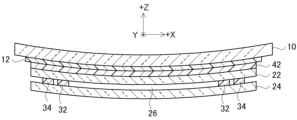
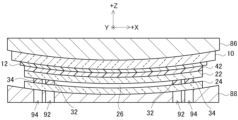
図1~図7を参照して、本実施形態に係る曲面液晶パネル100を説明する。曲面液晶パネル100は、図1、図2に示すように、曲面カバー10と液晶パネル20とを備える。曲面カバー10は、液晶パネル20を湾曲させて支持する。曲面カバー10と液晶パネル20は、接着層12により接着されている。液晶パネル20は、図示しない表示制御部と駆動回路からの信号により、文字、カラー画像等を表示する。本明細書では、理解を容易にするため、図1における曲面液晶パネル100の右方向(紙面の右方向)を+X方向、上方向(紙面の上方向)を+Y方向、+X方向と+Y方向に垂直な方向(紙面の手前方向)を+Z方向として説明する。
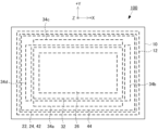
第1基板22と第2基板24は、第1シール部32と第2シール部34により、所定の間隔(セルギャップ)に貼り合わされている。
実施形態1では、第2シール部34は枠形状を有している。第2シール部34の形状は任意である。第2シール部34は、第1基板22と第2基板24が湾曲するまでの間、第1基板22と第2基板24が貼り合わせられている状態を維持すればよい。
実施形態1と実施形態2では、曲面液晶パネル100は第1シール部32と第2シール部34とを有している。曲面液晶パネル100は他のシール部を有してもよい。
以上、実施形態を説明したが、本開示は、要旨を逸脱しない範囲で種々の変更が可能である。
Claims (8)
- 第1方向に湾曲した第1基板と、
前記第1方向に湾曲し、前記第1基板に対向する第2基板と、
前記第1基板と前記第2基板に挟持された液晶と、
前記第1基板と前記第2基板とを貼り合わせ、前記液晶を封入する第1シール部と、
前記第1シール部の外周を囲む第2シール部と、を備え、
前記第2シール部の前記第1基板と前記第2基板とを貼り合わせる力は、前記第1シール部の前記第1基板と前記第2基板とを貼り合わせる力よりも、弱い、
曲面液晶パネル。 - 前記第2シール部は、複数に分割されている、
請求項1に記載の曲面液晶パネル。 - 前記第2シール部は、解体性接着剤又は解体性粘着剤から形成されている、
請求項1又は2に記載の曲面液晶パネル。 - 前記第1シール部は、前記第1基板と前記第2基板が前記第1方向に湾曲した状態で、硬化する、
請求項1から3のいずれか1項に記載の曲面液晶パネル。 - 平面視した場合に、前記第1基板又は前記第2基板の湾曲の稜線の上、かつ前記第2シール部の外側に配置され、前記第1基板と前記第2基板とを貼り合わせる第3シール部を備える、
請求項1から4のいずれか1項に記載の曲面液晶パネル。 - 第1基板と第2基板のうちの一方に液晶を封入する第1シール部を形成する工程と、
前記第1シール部を形成された前記第1基板と前記第2基板のうちの一方に、前記第1シール部の外周を囲む第2シール部を形成する工程と、
前記第1シール部と前記第2シール部とを形成された前記第1基板と前記第2基板のうちの一方と、前記第1基板と前記第2基板のうちの他方とを重ね合わせる工程と、
前記第2シール部を硬化させ、前記第1基板と前記第2基板とを貼り合わせる工程と、
貼り合わされた前記第1基板と前記第2基板とを第1方向に湾曲させる工程と、
前記第1基板と前記第2基板が湾曲した状態で、硬化した前記第2シール部の前記第1基板と前記第2基板とを貼り合わせる力を弱める工程と、
前記第1基板と前記第2基板が湾曲した状態で、前記第1シール部を硬化させる工程と、を含み、
前記第2シール部の弱められた前記第1基板と前記第2基板とを貼り合わせる力は、硬化した前記第1シール部の前記第1基板と前記第2基板とを貼り合わせる力よりも、弱い、
曲面液晶パネルの製造方法。 - 前記第1シール部を形成する工程と前記重ね合わせる工程との間に、前記第1シール部に囲まれた領域に前記液晶を滴下する工程を含む、
請求項6に記載の曲面液晶パネルの製造方法。 - 前記貼り合わせる工程と前記湾曲させる工程との間に、前記第1シール部に囲まれた領域に前記液晶を注入し、封止する工程を含む、
請求項6に記載の曲面液晶パネルの製造方法。
Priority Applications (3)
| Application Number | Priority Date | Filing Date | Title |
|---|---|---|---|
| JP2020209796A JP7522650B2 (ja) | 2020-12-18 | 2020-12-18 | 曲面液晶パネル及び曲面液晶パネルの製造方法 |
| US17/549,197 US11733566B2 (en) | 2020-12-18 | 2021-12-13 | Curved liquid crystal panel and manufacturing method for curved liquid crystal panel |
| CN202111514862.2A CN114647118B (zh) | 2020-12-18 | 2021-12-13 | 弯曲液晶面板和用于弯曲液晶面板的制造方法 |
Applications Claiming Priority (1)
| Application Number | Priority Date | Filing Date | Title |
|---|---|---|---|
| JP2020209796A JP7522650B2 (ja) | 2020-12-18 | 2020-12-18 | 曲面液晶パネル及び曲面液晶パネルの製造方法 |
Publications (2)
| Publication Number | Publication Date |
|---|---|
| JP2022096694A JP2022096694A (ja) | 2022-06-30 |
| JP7522650B2 true JP7522650B2 (ja) | 2024-07-25 |
Family
ID=81991915
Family Applications (1)
| Application Number | Title | Priority Date | Filing Date |
|---|---|---|---|
| JP2020209796A Active JP7522650B2 (ja) | 2020-12-18 | 2020-12-18 | 曲面液晶パネル及び曲面液晶パネルの製造方法 |
Country Status (3)
| Country | Link |
|---|---|
| US (1) | US11733566B2 (ja) |
| JP (1) | JP7522650B2 (ja) |
| CN (1) | CN114647118B (ja) |
Families Citing this family (1)
| Publication number | Priority date | Publication date | Assignee | Title |
|---|---|---|---|---|
| CN116088229B (zh) * | 2023-01-30 | 2025-02-07 | 华映科技(集团)股份有限公司 | 一种采用厚度不同的框胶的曲面液晶显示面板 |
Citations (1)
| Publication number | Priority date | Publication date | Assignee | Title |
|---|---|---|---|---|
| US20190107750A1 (en) | 2016-12-23 | 2019-04-11 | HKC Corporation Limited | Curved display panel and curved display apparatus |
Family Cites Families (11)
| Publication number | Priority date | Publication date | Assignee | Title |
|---|---|---|---|---|
| JP5239152B2 (ja) * | 2006-02-02 | 2013-07-17 | セイコーエプソン株式会社 | 電気光学装置の製造方法、及び電子機器 |
| JP2008175914A (ja) * | 2007-01-16 | 2008-07-31 | Sharp Corp | 曲面液晶セルの製造方法及び曲面液晶パネルの製造方法 |
| JP5092965B2 (ja) * | 2008-07-23 | 2012-12-05 | 三菱電機株式会社 | 湾曲型液晶パネル及びその液晶パネルの製造方法 |
| TWI521286B (zh) * | 2013-12-20 | 2016-02-11 | 友達光電股份有限公司 | 薄化顯示面板及其製造方法 |
| CN104865723B (zh) * | 2015-05-07 | 2017-09-19 | 武汉华星光电技术有限公司 | 一种曲面液晶显示面板的制程方法 |
| JP2017090528A (ja) * | 2015-11-04 | 2017-05-25 | 株式会社ジャパンディスプレイ | 表示装置 |
| JP2017181821A (ja) | 2016-03-30 | 2017-10-05 | パナソニック液晶ディスプレイ株式会社 | 曲面ディスプレイを備えた車載デバイス |
| CN106125359B (zh) * | 2016-06-29 | 2019-04-02 | 京东方科技集团股份有限公司 | 一种曲面显示面板的制作方法、曲面显示面板及显示装置 |
| KR20190083027A (ko) * | 2018-01-02 | 2019-07-11 | 삼성디스플레이 주식회사 | 표시패널 및 그 제조방법 |
| KR102795420B1 (ko) * | 2020-02-25 | 2025-04-14 | 삼성디스플레이 주식회사 | 표시 장치 및 표시 장치의 제조 방법 |
| CN111951680B (zh) * | 2020-08-20 | 2022-09-30 | 京东方科技集团股份有限公司 | 一种胶膜、柔性显示面板、制作方法以及胶膜去除方法 |
-
2020
- 2020-12-18 JP JP2020209796A patent/JP7522650B2/ja active Active
-
2021
- 2021-12-13 US US17/549,197 patent/US11733566B2/en active Active
- 2021-12-13 CN CN202111514862.2A patent/CN114647118B/zh active Active
Patent Citations (1)
| Publication number | Priority date | Publication date | Assignee | Title |
|---|---|---|---|---|
| US20190107750A1 (en) | 2016-12-23 | 2019-04-11 | HKC Corporation Limited | Curved display panel and curved display apparatus |
Also Published As
| Publication number | Publication date |
|---|---|
| CN114647118A (zh) | 2022-06-21 |
| US20220197068A1 (en) | 2022-06-23 |
| US11733566B2 (en) | 2023-08-22 |
| JP2022096694A (ja) | 2022-06-30 |
| CN114647118B (zh) | 2025-11-28 |
Similar Documents
| Publication | Publication Date | Title |
|---|---|---|
| JP4494446B2 (ja) | 表示装置 | |
| CN101118353B (zh) | 液晶显示装置 | |
| US20140226111A1 (en) | Method for manufacturing curved-surface display | |
| JP5926050B2 (ja) | 液晶表示装置 | |
| JP2009048214A (ja) | 表示装置の製造方法、及び、貼り合わせ方法 | |
| WO2011062009A1 (ja) | 液晶パネルおよび液晶表示装置 | |
| WO2012042787A1 (ja) | 液晶モジュール及び電子機器 | |
| WO2010058502A1 (ja) | 液晶表示装置及びその製造方法 | |
| JP2013073175A (ja) | 液晶表示装置 | |
| JP4335632B2 (ja) | 液晶表示装置の製造方法 | |
| KR101700265B1 (ko) | 액정패널의 제조방법 | |
| JP7522650B2 (ja) | 曲面液晶パネル及び曲面液晶パネルの製造方法 | |
| JP4227625B2 (ja) | 表示装置 | |
| JP2017181821A (ja) | 曲面ディスプレイを備えた車載デバイス | |
| JP2005141199A (ja) | 液晶ディスプレイセルとその製造方法 | |
| CN103376585A (zh) | 液晶显示装置的制造方法 | |
| JP4414061B2 (ja) | 液晶表示装置およびその製造方法 | |
| JP2014071438A (ja) | 液晶表示装置 | |
| JP5309840B2 (ja) | 保護板一体型液晶表示パネルの製造方法 | |
| CN211123549U (zh) | 液晶显示装置 | |
| KR20080076042A (ko) | 액정 표시 장치의 제조 방법 | |
| JP2007264102A (ja) | 液晶表示パネルおよびその製造方法 | |
| JP2023097636A (ja) | 液晶表示パネル、液晶表示装置及び液晶表示装置の製造方法 | |
| JP2007010706A (ja) | 液晶装置及びその製造方法 | |
| JP2012008492A (ja) | 液晶素子の製造方法 |
Legal Events
| Date | Code | Title | Description |
|---|---|---|---|
| A621 | Written request for application examination |
Free format text: JAPANESE INTERMEDIATE CODE: A621 Effective date: 20231026 |
|
| A977 | Report on retrieval |
Free format text: JAPANESE INTERMEDIATE CODE: A971007 Effective date: 20240531 |
|
| TRDD | Decision of grant or rejection written | ||
| A01 | Written decision to grant a patent or to grant a registration (utility model) |
Free format text: JAPANESE INTERMEDIATE CODE: A01 Effective date: 20240618 |
|
| A61 | First payment of annual fees (during grant procedure) |
Free format text: JAPANESE INTERMEDIATE CODE: A61 Effective date: 20240712 |
|
| R150 | Certificate of patent or registration of utility model |
Ref document number: 7522650 Country of ref document: JP Free format text: JAPANESE INTERMEDIATE CODE: R150 |