EP3512002B1 - Connecteur de cellule destiné à la connexion électrique des bornes de cellule d'un dispositif accumulateur d'énergie - Google Patents
Connecteur de cellule destiné à la connexion électrique des bornes de cellule d'un dispositif accumulateur d'énergie Download PDFInfo
- Publication number
- EP3512002B1 EP3512002B1 EP18213915.4A EP18213915A EP3512002B1 EP 3512002 B1 EP3512002 B1 EP 3512002B1 EP 18213915 A EP18213915 A EP 18213915A EP 3512002 B1 EP3512002 B1 EP 3512002B1
- Authority
- EP
- European Patent Office
- Prior art keywords
- cell connector
- compensating element
- cell
- elements
- conductor track
- Prior art date
- Legal status (The legal status is an assumption and is not a legal conclusion. Google has not performed a legal analysis and makes no representation as to the accuracy of the status listed.)
- Active
Links
Images

Classifications
-
- H—ELECTRICITY
- H01—ELECTRIC ELEMENTS
- H01M—PROCESSES OR MEANS, e.g. BATTERIES, FOR THE DIRECT CONVERSION OF CHEMICAL ENERGY INTO ELECTRICAL ENERGY
- H01M50/00—Constructional details or processes of manufacture of the non-active parts of electrochemical cells other than fuel cells, e.g. hybrid cells
- H01M50/50—Current conducting connections for cells or batteries
- H01M50/502—Interconnectors for connecting terminals of adjacent batteries; Interconnectors for connecting cells outside a battery casing
- H01M50/503—Interconnectors for connecting terminals of adjacent batteries; Interconnectors for connecting cells outside a battery casing characterised by the shape of the interconnectors
-
- H—ELECTRICITY
- H01—ELECTRIC ELEMENTS
- H01M—PROCESSES OR MEANS, e.g. BATTERIES, FOR THE DIRECT CONVERSION OF CHEMICAL ENERGY INTO ELECTRICAL ENERGY
- H01M50/00—Constructional details or processes of manufacture of the non-active parts of electrochemical cells other than fuel cells, e.g. hybrid cells
- H01M50/50—Current conducting connections for cells or batteries
- H01M50/502—Interconnectors for connecting terminals of adjacent batteries; Interconnectors for connecting cells outside a battery casing
- H01M50/521—Interconnectors for connecting terminals of adjacent batteries; Interconnectors for connecting cells outside a battery casing characterised by the material
- H01M50/522—Inorganic material
-
- Y—GENERAL TAGGING OF NEW TECHNOLOGICAL DEVELOPMENTS; GENERAL TAGGING OF CROSS-SECTIONAL TECHNOLOGIES SPANNING OVER SEVERAL SECTIONS OF THE IPC; TECHNICAL SUBJECTS COVERED BY FORMER USPC CROSS-REFERENCE ART COLLECTIONS [XRACs] AND DIGESTS
- Y02—TECHNOLOGIES OR APPLICATIONS FOR MITIGATION OR ADAPTATION AGAINST CLIMATE CHANGE
- Y02E—REDUCTION OF GREENHOUSE GAS [GHG] EMISSIONS, RELATED TO ENERGY GENERATION, TRANSMISSION OR DISTRIBUTION
- Y02E60/00—Enabling technologies; Technologies with a potential or indirect contribution to GHG emissions mitigation
- Y02E60/10—Energy storage using batteries
Definitions
- the invention relates to a cell connector for the electrical connection of cell terminals of an energy storage device, having contacting elements for connection to at least one cell terminal and a compensating element electrically connecting two contacting elements with at least one resilient conductor path.
- Cell connectors are from the WO 2009/080148 A2 known in the form of a solid high-current bridging bar perforated at both ends between adjacent opposite cell poles of individual electrochemical cells to be connected in series to the battery pack.
- Compensating sleeves are inserted into the holes of each cell connector, the outer diameter of which is smaller and the axial length of which is greater than the respective hole.
- the freely protruding poles of the cells engage in these sleeves.
- Each of the compensating sleeves is shifted within its hole according to the tolerances of the pole positions caused by production.
- the individually positioned compensating sleeves are then welded to their cell poles on the one hand and to the cell connector on the other.
- the compensating area consists of several metallic layers separated by foils, which, due to a curvature upwards, enable elastic length compensation and thus a movement of the poles towards one another.
- More cell connector with a certain flexibility in the connection area between the contact areas of the cell terminals are from DE 10 2011 075 835 A1 , the DE 10 2009 058 723 A1 , the DE 10 2015 201 792 A1 and the DE 10 2010 019 708 A1 known.
- the invention is based on the consideration that increasingly flat cell connectors are advantageous due to ever tighter construction specifications. At the same time, however, these must compensate for both position and assembly tolerances and a changing distance between the individual cell terminals when charging and discharging the energy storage device. Due to the position of the conductor path completely in one plane with the two contacting elements, a very flat cell connector can be achieved, which enables the entire energy storage device to be constructed in a compact manner.
- the resilient conductor track can compensate for position and assembly tolerances as well as movements of the cell terminals relative to one another without excessive forces acting on the cell terminals.
- the two contacting elements of the cell connector can have a flat metal sheet, consist of the flat metal sheet on their upper side or in their entirety. On their underside, the contacting elements can have one or more fastening elements, with which the cell connector is fastened to the respective cell terminal during assembly of the energy storage device.
- the fastening elements can protrude downwards out of the plane defined by the two contacting elements.
- the course of the conductor track completely in the plane of the two contacting elements can be understood such that the two contacting elements are planar elements with a predetermined thickness, in particular a constant thickness over a contacting region, the thickness being understood perpendicularly to this plane.
- the plane can now range of this thickness are expediently parallel to an upper side of the contacting elements.
- the conductor track lies entirely in this plane of the two contacting elements.
- the conductor track can protrude upwards and/or downwards beyond the contacting elements, but it is important that they have their full length from one to the other contacting element in the plane, so the plane runs through this full length of the conductor track.
- the cell connector can be particularly compact if the thickness of the conductor track lies entirely within the thickness of the two contacting elements.
- the conductor track has a material cross section that is smaller than the material cross section of the contacting elements.
- the cross-section of the material is expediently to be seen transversely to the direction of current flow during regular operation of the cell connector.
- the conductor track can have a plurality of conductor elements which are expediently arranged parallel to one another in the direction of current flow.
- the compensating element can have a plurality of metal layers stacked on top of one another, for example a plurality of metal sheets one on top of the other. These are expediently placed one on top of the other in an electrically contacting manner over their entire length and can be connected to one another in a material-locking manner, for example by welding to one another.
- the area in which the plane formed by the contacting elements can lie can extend over all such layers.
- the installation height of the energy storage device can be kept low by the two-dimensional construction of conductor tracks with the two contacting elements. However, there may be space available in the width direction. Such a space can be used effectively if the conductor track projects beyond the width of the contacting elements in the width direction. The current-carrying capacity and/or the elasticity of the conductor track or its resilience can be increased as a result.
- Length direction, width direction and thickness are appropriately to be understood as a three-dimensional and orthogonal direction system, the length direction being the direction from one contacting element to the other or from one cell terminal to the other cell terminal connected to it, the width direction also in the Level of the two contacting elements runs and the thickness direction is perpendicular to the first two directions.
- a compact cell connector that is efficient in terms of current-carrying capacity can be achieved if the two contacting elements and the compensating element are designed as a flat metal sheet. All three elements expediently form a common metal sheet, that is to say they are made together in one piece.
- the sheet metal can be of uniform thickness over its entire length over the two contacting elements and the compensating element both in the length direction and in the width direction. It is also possible that the sheet metal is thicker in the area of the compensating element than in the area of the two contacting elements.
- a simple production of the cell connector can be achieved if the two contacting elements and the compensating element are together a stamped part.
- the conduction path can be produced in a simple manner. It is also possible to cut the contacting elements and the compensating element by means of a water jet or laser or the like, with the stamped part and part cut in a different way being referred to as a cut part in the generic term.
- the conductor path is designed to be resilient, in particular due to its narrowing compared to the contacting elements, so that it compensates for changes in the position of the two cell terminals relative to one another.
- the line path in the compensating element has a change in direction of at least 90°. At least a part of the conductor track runs through it at an angle, in particular perpendicular to the length direction, so that an advantageous spring effect is achieved.
- the spring effect can be further increased if the line path in the compensating element has at least two opposite changes in direction of at least 70°.
- the line path forms a U shape in the compensating element. This can be in the plane with the two contacting elements and transverse to an imaginary line connecting the two cell terminals or the two Contacting elements connected to each other. This connecting line can be in the longitudinal direction.
- a further improvement in the spring effect can be achieved if the line path forms a meandering shape in the compensating element.
- a meander shape can be understood as a line that winds back and forth with two opposite turns of at least 150° each, in particular at least 240° each, and a turning point lying between the turns.
- the conductor track opens into the two contacting elements in the opposite direction.
- the openings of the conductor path into the two contacting elements run antiparallel to one another.
- the conductor path has an odd number of kinks, with three kinks, in particular only one kink, being advantageous.
- kinks do not have to be sharp, but can—regardless of their number—also be in a rounded form, in particular to avoid peaks in the current density in the area of too narrow radii.
- the thickness of the compensating element is greater than a thickness of the two contacting elements.
- a particularly flat structure of the cell connector is realized according to the invention in that the two contacting elements and the compensating element together form a stepped band.
- the step band has at least two thicknesses, a first thickness in the area of the contacting elements and a second, larger thickness in the area of the compensating element. The greater thickness in the area of the compensating element can thus be achieved without a joining process for two sheets or strips placed one on top of the other, so that there is a uniform electrical resistance without interference areas caused by joining.
- a step strip can be designed with a high current-carrying capacity and yet also relatively flat in the area of greater thickness, so that the cell connector can be designed to be flat overall.
- a step strip can be a strip or sheet metal that has two thicknesses in one piece, with the two thickness regions being separated from one another by a step.
- the step direction is expediently in the width direction.
- a greater thickness of the compensating element can be achieved by means of a second metal strip level, which rests on an expediently continuous first metal strip level and is joined to it.
- the compensating element has a greater thickness than the two contacting elements.
- the contacting elements can also have the thickness of the compensating element in a transition area.
- the transition area is smaller than half of a contacting element.
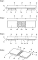
- FIG 1 shows a cell connector 2a for connecting two cell terminals 4 of an energy storage device, which is shown in FIG 1 are only indicated schematically.
- the cell connector 2a comprises two contacting elements 6a, to each of which a fastening element 8 is materially attached, for example by welding.
- the fastening elements 8 are each connected to their cell terminal 4, expediently also in a materially bonded manner.
- a contacting element 6a forms a contacting unit with its fastening element 8 .
- the two Contacting elements 6a are connected to one another via a compensating element 10a.
- the cell connector 2a is in FIG 2 shown in a plan view.
- FIG 2 shows the cell connector 2a with the two contacting elements 6a and the compensating element 10a.
- the compensating element 10a contains a line path 12a with two line elements 14a, which mechanically and electrically connect the two contacting elements 6a to one another.
- the two contacting elements 6a and the compensating element 10a are made from a continuous, flat metal strip or sheet metal.
- the compensating element 10a contains a line path 12a with one or more line elements 14a. These can be cut out of the strip or sheet metal by stamping or another cutting process. Due to the geometry of the line elements 14a, the line path 12a is resilient, so that it allows compensation between the contacting elements 6a in three translatory and three rotary directions of movement. Manufacturing tolerances of the energy storage device and operational or transport-related movements of the cell terminals 4 relative to each other can be resiliently compensated for in this way without the contacting elements 6a or the cell connector 2a being mechanically loaded in an impermissible manner.
- the conductor track 12a or the compensating element 10a runs completely in the plane of the contacting elements 6a.
- two levels 16 are indicated by dot-dash lines, which lie in the top of the contacting elements 6a and the bottom of the contacting elements 6a.
- the compensating element 10a or its conductor track 12a with all of its material lies completely between these two planes 16.
- the conductor track 12a also runs completely in one plane with the two contacting elements 6a if any plane that lies between the two in FIG 1 Levels 16 shown is located, runs through the entire conductor track 12a, wherein the conductor track 12a can protrude above or below the contacting elements 6a or their levels 16.
- the cell connector 2a is off FIG 1 divided into three areas 18, 20.
- the contacting elements 6a are each in their contacting area 18 and the compensating element 10a is in a compensating area 20.
- the border between the areas 18, 20 is formed by the line at which the contacting elements 6a tapers in the longitudinal direction 22 towards the conductor track 12a, so that the current-carrying material cross-section in the longitudinal direction 22 is thereby compared to the material cross-section of the contacting element 6a scaled down.
- the exemplary embodiment shown is designed like the previous one, with the difference that the contacting elements 6b and the compensating element 10b are formed by a metal step band.
- the descriptions of the embodiment 3 and the following exemplary embodiments are essentially limited to the differences from the respective preceding exemplary embodiment, to which reference is made with regard to features and functions that remain the same.
- all features of a previous exemplary embodiment are generally adopted in the respective following exemplary embodiment without being described again, unless features are described as differences from the previous exemplary embodiment.
- the step band is thicker in the area of the compensating element 10b than in the majority of the area of the two contacting elements 6b.
- the contacting area 18 extends to the tapering of the material or the line elements 14b of the line track 12b, with these looking exactly like this together with the contacting elements 6b in the plan view in FIG 2 shown, apart from the additional steps 24 visible from above.
- the thickness of the step band is greater in part of the contacting area 18, ie in part of the contacting element 6b, than in the remaining part of the contacting area 18 or contacting element 6b.
- the flatter part of the contacting elements 6b is larger than the thicker part of the area 18 or contacting element 6b. Due to the greater thickness of the compensating element 10b, the current-carrying material cross section in the region of the conductor track 12b can be different than in the exemplary embodiment FIG 1 be increased so that the current-carrying capacity is increased.
- the cell connector 2c is very similar in its geometry to that in the exemplary embodiment FIG 2 executed.
- FIG 4 shows the cell connector 2c in perspective, so that the length direction 22 from one contacting element 6c to the other as well as the width direction 26 and the thickness direction 28 are clearly visible.
- the compensating element 10c is designed with a line path 12c with two meandering line elements 14c, which, however, are arranged completely next to one another and not as in the exemplary embodiment FIG 2 partially intertwined.
- the line elements 14a, 14c are designed with three kinks in one direction and three kinks in the opposite direction, each at 90°. Rounding does not change the designation of a kink. There are therefore three changes of direction of 90° in the same direction and three changes of direction of 90° in opposite directions in each case.
- the Figures 5 to 8 show four conduction path principles or geometries 12d-12g that can be used according to the invention.
- the contacting elements 6d are connected to one another by straight, kink-free and bend-free line elements 14d. These allow a movement of the contacting elements 6d in four dimensions relative to one another, in two translational directions and two rotational directions. A compensation in the longitudinal direction 22 is not possible.
- the spring action of the compensating element 10e between the two contacting elements 6e is given in all six dimensions.
- the line elements 14e have two kinks, each at 90° in opposite directions 5 are rigid, allows.
- FIG 7 An even more elastic spring effect in the longitudinal direction 22 is achieved by the exemplary embodiment FIG 7 achieved, in which the line elements 14f of the line path 12f each have four kinks of 90° each.
- the spring action in the longitudinal direction 22 is further improved by the line elements 14g of the line track 12g having a simple meandering shape, which has two kinks of 90° each in one direction and then two kinks of 90° each in the other direction. Due to the change in direction, there is a turning point of the line elements 14g between the two kinks in each case.
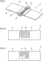
- the exemplary embodiment 9 resembles that of in its thickness profile 3 , However, instead of the stepped strip, a second sheet metal plane or a second flat sheet metal or strip element 32 connects the two contacting elements 6h to one another.
- the predominant part of the contacting elements 6h is thus formed by a single metal band 30, the compensating element 10h with its line path 12h with its four line elements 14h being formed by the two metal bands 30, 32.
- the two metal bands 30, 32 lie flat on top of one another and are joined together in a materially bonded manner, for example by welding.
- the four line elements 14h each form a U-shape that lies in the plane with the two contacting elements 6h and transverse to an imaginary connecting line that connects the two cell terminals 4 to one another, the U-shapes are therefore in the width direction 26.
- Two line elements 14h each engage in the same direction with both U-legs in one another. In order to achieve a high spring effect, the line elements 14h also protrude in the width direction 26 beyond the contacting elements 6h.
- the Figures 10 and 11 12 show two exemplary embodiments with line paths 12i, 12j with line elements 14i, 14j that have an odd number of kinks in the exemplary embodiment 10 there are each a single kink and in the embodiment 11 there are three kinks each.
- a relatively large number of line elements 14i, 14j can be integrated in a small space, so that a high current-carrying capacity can be achieved.
- the spring effect of the compensating elements 10i, 10j is - precisely in the exemplary embodiment 10 - limited by the low number of buckling.
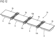
- FIG. 12 shows an embodiment in which more than two contacting elements 6k are separated from one another by a plurality of compensating elements 10k.
- the geometry of the compensating elements 10k is the same as in the exemplary embodiment 9 - Aside from only a single existing metal band, but can also be made in any other geometry, as explained in the previous embodiments.
- a compensating element 10k is located between two adjacent contacting elements 6k, so that the contacting elements 6k are resiliently mounted largely independently of one another.
- the number of contacting elements 6k and the compensating elements 10k located between them is essentially arbitrary.
Landscapes
- Chemical & Material Sciences (AREA)
- Chemical Kinetics & Catalysis (AREA)
- Electrochemistry (AREA)
- General Chemical & Material Sciences (AREA)
- Inorganic Chemistry (AREA)
- Battery Mounting, Suspending (AREA)
- Connection Of Batteries Or Terminals (AREA)
Claims (11)
- Connecteur de cellule (2a-k) destiné à la connexion électrique de bornes de cellule (4) d'un dispositif accumulateur d'énergie, présentant des éléments de mise en contact (6a-k) destinés à la connexion à respectivement au moins une borne de cellule (4), et un élément de compensation (10a-k) connectant électriquement deux éléments de mise en contact (6a-k) l'un à l'autre et doté d'au moins une piste conductive élastique (12a-k), la piste conductive (12a-k) s'étendant entièrement dans un plan comprenant les deux éléments de mise en contact (6a-k),
caractérisé en ce que les deux éléments de mise en contact (6b) et l'élément de compensation (10b) forment ensemble une bande étagée ayant une première épaisseur dans la zone des deux éléments de mise en contact (6b) et une deuxième épaisseur, plus grande, dans la zone de l'élément de compensation (10b). - Connecteur de cellule selon la revendication 1, caractérisé en ce que la piste conductive (12a-k) présente une section transversale de matériau qui est inférieure à la section transversale de matériau des éléments de mise en contact (6a-k).
- Connecteur de cellule selon la revendication 1 ou 2, caractérisé en ce que la piste conductive (12h) fait saillie dans la direction de la largeur (26) au-delà de la largeur des éléments de mise en contact (6h).
- Connecteur de cellule selon l'une quelconque des revendications précédentes, caractérisé en ce que les deux éléments de mise en contact (6a, 6b-g, 6k) et l'élément de compensation (10a, 10b-g, 10k) sont réalisés sous la forme d'une tôle métallique plane.
- Connecteur de cellule selon l'une quelconque des revendications précédentes, caractérisé en ce que les deux éléments de mise en contact (6a-g, 6i-k) et l'élément de compensation (10a-g, 10i-k) sont ensemble une pièce découpée.
- Connecteur de cellule selon l'une quelconque des revendications précédentes, caractérisé en ce que la piste conductive (12a-c, 12e-k) dans l'élément de compensation (10a-c, 10e-k) présente un changement de direction d'au moins 90°.
- Connecteur de cellule selon l'une quelconque des revendications précédentes, caractérisé en ce que la piste conductive (12a-c, 12f-h, 12j-k) dans l'élément de compensation (10a-c, 10f-h, 10j-k) présente au moins deux changements de direction opposés d'au moins 70°.
- Connecteur de cellule selon l'une quelconque des revendications précédentes, caractérisé en ce que la piste conductive (12a-b, 12f, 12h, 12j-k) dans l'élément de compensation (10a-b, 10f, 10h, 10j-k) constitue une forme de U qui se situe dans le plan comprenant les deux éléments de mise en contact (6a-b, 6f, 6h, 6j-k) et transversalement à une ligne de liaison imaginaire qui relie les deux bornes de cellule (8) .
- Connecteur de cellule selon l'une quelconque des revendications précédentes, caractérisé en ce que la piste conductive (12a-c, 12g) dans l'élément de compensation (10a-c, 10g) constitue une forme de méandre.
- Connecteur de cellule selon l'une quelconque des revendications précédentes, caractérisé en ce que la piste conductive (12e-f) présente un nombre impair de coudes.
- Connecteur de cellule selon l'une quelconque des revendications précédentes, caractérisé en ce que l'élément de compensation (10h) présente au moins deux plans de bande métallique (30, 32) de sorte que l'élément de compensation (10h) présente une plus grande épaisseur que les deux éléments de mise en contact (6h).
Applications Claiming Priority (1)
| Application Number | Priority Date | Filing Date | Title |
|---|---|---|---|
| DE102018000258.7A DE102018000258A1 (de) | 2018-01-13 | 2018-01-13 | Zellverbinder zur elektrischen Verbindung von Zellterminals einer Energiespeichereinrichtung |
Publications (2)
| Publication Number | Publication Date |
|---|---|
| EP3512002A1 EP3512002A1 (fr) | 2019-07-17 |
| EP3512002B1 true EP3512002B1 (fr) | 2022-01-19 |
Family
ID=64746088
Family Applications (1)
| Application Number | Title | Priority Date | Filing Date |
|---|---|---|---|
| EP18213915.4A Active EP3512002B1 (fr) | 2018-01-13 | 2018-12-19 | Connecteur de cellule destiné à la connexion électrique des bornes de cellule d'un dispositif accumulateur d'énergie |
Country Status (2)
| Country | Link |
|---|---|
| EP (1) | EP3512002B1 (fr) |
| DE (1) | DE102018000258A1 (fr) |
Cited By (1)
| Publication number | Priority date | Publication date | Assignee | Title |
|---|---|---|---|---|
| WO2025215350A1 (fr) * | 2024-04-08 | 2025-10-16 | Danecca Group Limited | Barre omnibus et module de batterie la comprenant |
Families Citing this family (4)
| Publication number | Priority date | Publication date | Assignee | Title |
|---|---|---|---|---|
| DE102021112321A1 (de) | 2021-05-11 | 2022-11-17 | Yazaki Systems Technologies Gmbh | Zellverbinder für einen elektrischen Energiespeicher und elektrischer Energiespeicher mit dem Zellverbinder |
| JP7393394B2 (ja) * | 2021-08-06 | 2023-12-06 | 矢崎総業株式会社 | バスバ |
| EP4489209A1 (fr) * | 2023-07-04 | 2025-01-08 | Valmet Automotive Oyj | Barre omnibus et procédé |
| DE102024106216A1 (de) * | 2024-03-04 | 2025-09-04 | Lisa Dräxlmaier GmbH | Leitungsanordnung sowie Fahrzeug mit einer solchen Leitungsanordnung |
Citations (1)
| Publication number | Priority date | Publication date | Assignee | Title |
|---|---|---|---|---|
| DE102009058723B4 (de) * | 2009-12-17 | 2011-12-01 | Amphenol-Tuchel Electronics Gmbh | Flexibler Zellverbinder |
Family Cites Families (8)
| Publication number | Priority date | Publication date | Assignee | Title |
|---|---|---|---|---|
| US5578392A (en) * | 1995-02-17 | 1996-11-26 | Japan Storage Battery Co., Ltd. | Cylindrical cell, a cell pack, and a cell holder |
| JP2002246005A (ja) * | 2001-02-21 | 2002-08-30 | Toshiba Battery Co Ltd | 電池接続構造体 |
| DE102007063177A1 (de) | 2007-12-20 | 2009-06-25 | Daimler Ag | Zellverbinder, Verfahren zum Verbinden zweier Pole von Zellen von Batterien und Batterie mit Zellverbinder |
| DE102009024513A1 (de) * | 2009-06-08 | 2010-12-09 | Auto-Kabel Managementgesellschaft Mbh | Batteriezellenverbinder |
| DE102010019708A1 (de) * | 2010-05-07 | 2011-11-10 | Bayerische Motoren Werke Aktiengesellschaft | Speicherzellenverbinder und Speichermodul |
| DE102011075835A1 (de) * | 2011-05-13 | 2012-11-15 | Elringklinger Ag | Zellverbinder |
| DE102011080977A1 (de) | 2011-08-16 | 2013-02-21 | Sb Limotive Company Ltd. | Zellverbinder, Batteriezellenmodul, Batterie, Verfahren zur Herstellung eines Zellverbinders und Kraftfahrzeug |
| DE102015201792A1 (de) * | 2015-02-03 | 2016-08-04 | Robert Bosch Gmbh | Zellverbinder zur elektrisch leitenden Verbindung von Batteriezellen sowie Batteriesystem |
-
2018
- 2018-01-13 DE DE102018000258.7A patent/DE102018000258A1/de not_active Withdrawn
- 2018-12-19 EP EP18213915.4A patent/EP3512002B1/fr active Active
Patent Citations (1)
| Publication number | Priority date | Publication date | Assignee | Title |
|---|---|---|---|---|
| DE102009058723B4 (de) * | 2009-12-17 | 2011-12-01 | Amphenol-Tuchel Electronics Gmbh | Flexibler Zellverbinder |
Cited By (1)
| Publication number | Priority date | Publication date | Assignee | Title |
|---|---|---|---|---|
| WO2025215350A1 (fr) * | 2024-04-08 | 2025-10-16 | Danecca Group Limited | Barre omnibus et module de batterie la comprenant |
Also Published As
| Publication number | Publication date |
|---|---|
| DE102018000258A1 (de) | 2019-07-18 |
| EP3512002A1 (fr) | 2019-07-17 |
Similar Documents
| Publication | Publication Date | Title |
|---|---|---|
| EP3512002B1 (fr) | Connecteur de cellule destiné à la connexion électrique des bornes de cellule d'un dispositif accumulateur d'énergie | |
| EP1730818B1 (fr) | Connecteur electrique de type douille pour applications a courant eleve | |
| DE102007036646B4 (de) | Sicherungseinsatzeinheit | |
| DE69524702T2 (de) | Elektrischer Verbindungskasten | |
| EP3200261B1 (fr) | Système de mise en contact pour des éléments d'accumulateur d'énergie et accumulateur d'énergie | |
| DE102010054070B4 (de) | Thermoelektrische Vorrichtung und thermoelektrisches Modul | |
| DE102015206248B4 (de) | Batteriezellentrenner | |
| DE102018214363A1 (de) | Stromschiene, stromschienenmodul und batteriepack | |
| EP3224907B1 (fr) | Connecteur pour films de circuit imprimé flexibles | |
| DE102009030645B4 (de) | Brückerelement und Set aus zumindest einem Klemmelement und Brückerelement | |
| EP3482460B1 (fr) | Contact électrique à grande puissance | |
| DE102017220778A1 (de) | Kontaktelement | |
| DE3014118C2 (de) | Kontaktorgan | |
| WO2018130359A1 (fr) | Batterie, plaque de support et élément de plaque de support à éléments d'encliquetage | |
| EP0254770B1 (fr) | Dispositif de contact électrique | |
| EP2649684B1 (fr) | Connecteur haute puissance | |
| DE10117061A1 (de) | Elektrischer Verbinder | |
| EP4070406B1 (fr) | Barre omnibus pour une batterie | |
| DE102012223082A1 (de) | Kontaktelement und Verfahren zur Herstellung eines Kontaktelements | |
| DE102022112414A1 (de) | Flexibler Modulverbinder für eine Batterie und Batterie für ein Kraftfahrzeug | |
| EP1575076B1 (fr) | Porte-fusible pour des fusibles plats | |
| AT528006B1 (de) | Vorrichtung zum elektrischen Kontaktieren von Batteriezellen | |
| AT524120B1 (de) | Vorrichtung zum parallelen Kontaktieren mehrerer Batteriezellen mit einem Kontaktband | |
| DE102012217108B4 (de) | Verbindungselement zum elektrischen Verbinden von zwei Batteriezellen oder Batteriemodulen und Verfahren zum Herstellen eines solchen Verbindungselementes | |
| DE102006045433B3 (de) | Kernaufbau eines rechteckigen sekundären Lithium-Akkus |
Legal Events
| Date | Code | Title | Description |
|---|---|---|---|
| PUAI | Public reference made under article 153(3) epc to a published international application that has entered the european phase |
Free format text: ORIGINAL CODE: 0009012 |
|
| STAA | Information on the status of an ep patent application or granted ep patent |
Free format text: STATUS: THE APPLICATION HAS BEEN PUBLISHED |
|
| AK | Designated contracting states |
Kind code of ref document: A1 Designated state(s): AL AT BE BG CH CY CZ DE DK EE ES FI FR GB GR HR HU IE IS IT LI LT LU LV MC MK MT NL NO PL PT RO RS SE SI SK SM TR |
|
| AX | Request for extension of the european patent |
Extension state: BA ME |
|
| STAA | Information on the status of an ep patent application or granted ep patent |
Free format text: STATUS: REQUEST FOR EXAMINATION WAS MADE |
|
| 17P | Request for examination filed |
Effective date: 20200113 |
|
| RBV | Designated contracting states (corrected) |
Designated state(s): AL AT BE BG CH CY CZ DE DK EE ES FI FR GB GR HR HU IE IS IT LI LT LU LV MC MK MT NL NO PL PT RO RS SE SI SK SM TR |
|
| REG | Reference to a national code |
Ref country code: DE Ref legal event code: R079 Ref document number: 502018008569 Country of ref document: DE Free format text: PREVIOUS MAIN CLASS: H01M0002200000 Ipc: H01M0050502000 |
|
| RIC1 | Information provided on ipc code assigned before grant |
Ipc: H01M 50/502 20210101AFI20210621BHEP |
|
| GRAP | Despatch of communication of intention to grant a patent |
Free format text: ORIGINAL CODE: EPIDOSNIGR1 |
|
| STAA | Information on the status of an ep patent application or granted ep patent |
Free format text: STATUS: GRANT OF PATENT IS INTENDED |
|
| INTG | Intention to grant announced |
Effective date: 20210806 |
|
| GRAS | Grant fee paid |
Free format text: ORIGINAL CODE: EPIDOSNIGR3 |
|
| GRAA | (expected) grant |
Free format text: ORIGINAL CODE: 0009210 |
|
| STAA | Information on the status of an ep patent application or granted ep patent |
Free format text: STATUS: THE PATENT HAS BEEN GRANTED |
|
| AK | Designated contracting states |
Kind code of ref document: B1 Designated state(s): AL AT BE BG CH CY CZ DE DK EE ES FI FR GB GR HR HU IE IS IT LI LT LU LV MC MK MT NL NO PL PT RO RS SE SI SK SM TR |
|
| REG | Reference to a national code |
Ref country code: GB Ref legal event code: FG4D Free format text: NOT ENGLISH |
|
| REG | Reference to a national code |
Ref country code: CH Ref legal event code: EP |
|
| REG | Reference to a national code |
Ref country code: DE Ref legal event code: R096 Ref document number: 502018008569 Country of ref document: DE |
|
| REG | Reference to a national code |
Ref country code: AT Ref legal event code: REF Ref document number: 1464313 Country of ref document: AT Kind code of ref document: T Effective date: 20220215 |
|
| REG | Reference to a national code |
Ref country code: IE Ref legal event code: FG4D Free format text: LANGUAGE OF EP DOCUMENT: GERMAN |
|
| REG | Reference to a national code |
Ref country code: LT Ref legal event code: MG9D |
|
| REG | Reference to a national code |
Ref country code: NL Ref legal event code: MP Effective date: 20220119 |
|
| PG25 | Lapsed in a contracting state [announced via postgrant information from national office to epo] |
Ref country code: NL Free format text: LAPSE BECAUSE OF FAILURE TO SUBMIT A TRANSLATION OF THE DESCRIPTION OR TO PAY THE FEE WITHIN THE PRESCRIBED TIME-LIMIT Effective date: 20220119 |
|
| PG25 | Lapsed in a contracting state [announced via postgrant information from national office to epo] |
Ref country code: SE Free format text: LAPSE BECAUSE OF FAILURE TO SUBMIT A TRANSLATION OF THE DESCRIPTION OR TO PAY THE FEE WITHIN THE PRESCRIBED TIME-LIMIT Effective date: 20220119 Ref country code: RS Free format text: LAPSE BECAUSE OF FAILURE TO SUBMIT A TRANSLATION OF THE DESCRIPTION OR TO PAY THE FEE WITHIN THE PRESCRIBED TIME-LIMIT Effective date: 20220119 Ref country code: PT Free format text: LAPSE BECAUSE OF FAILURE TO SUBMIT A TRANSLATION OF THE DESCRIPTION OR TO PAY THE FEE WITHIN THE PRESCRIBED TIME-LIMIT Effective date: 20220519 Ref country code: NO Free format text: LAPSE BECAUSE OF FAILURE TO SUBMIT A TRANSLATION OF THE DESCRIPTION OR TO PAY THE FEE WITHIN THE PRESCRIBED TIME-LIMIT Effective date: 20220419 Ref country code: LT Free format text: LAPSE BECAUSE OF FAILURE TO SUBMIT A TRANSLATION OF THE DESCRIPTION OR TO PAY THE FEE WITHIN THE PRESCRIBED TIME-LIMIT Effective date: 20220119 Ref country code: HR Free format text: LAPSE BECAUSE OF FAILURE TO SUBMIT A TRANSLATION OF THE DESCRIPTION OR TO PAY THE FEE WITHIN THE PRESCRIBED TIME-LIMIT Effective date: 20220119 Ref country code: ES Free format text: LAPSE BECAUSE OF FAILURE TO SUBMIT A TRANSLATION OF THE DESCRIPTION OR TO PAY THE FEE WITHIN THE PRESCRIBED TIME-LIMIT Effective date: 20220119 Ref country code: BG Free format text: LAPSE BECAUSE OF FAILURE TO SUBMIT A TRANSLATION OF THE DESCRIPTION OR TO PAY THE FEE WITHIN THE PRESCRIBED TIME-LIMIT Effective date: 20220419 |
|
| PG25 | Lapsed in a contracting state [announced via postgrant information from national office to epo] |
Ref country code: PL Free format text: LAPSE BECAUSE OF FAILURE TO SUBMIT A TRANSLATION OF THE DESCRIPTION OR TO PAY THE FEE WITHIN THE PRESCRIBED TIME-LIMIT Effective date: 20220119 Ref country code: LV Free format text: LAPSE BECAUSE OF FAILURE TO SUBMIT A TRANSLATION OF THE DESCRIPTION OR TO PAY THE FEE WITHIN THE PRESCRIBED TIME-LIMIT Effective date: 20220119 Ref country code: GR Free format text: LAPSE BECAUSE OF FAILURE TO SUBMIT A TRANSLATION OF THE DESCRIPTION OR TO PAY THE FEE WITHIN THE PRESCRIBED TIME-LIMIT Effective date: 20220420 Ref country code: FI Free format text: LAPSE BECAUSE OF FAILURE TO SUBMIT A TRANSLATION OF THE DESCRIPTION OR TO PAY THE FEE WITHIN THE PRESCRIBED TIME-LIMIT Effective date: 20220119 |
|
| PG25 | Lapsed in a contracting state [announced via postgrant information from national office to epo] |
Ref country code: IS Free format text: LAPSE BECAUSE OF FAILURE TO SUBMIT A TRANSLATION OF THE DESCRIPTION OR TO PAY THE FEE WITHIN THE PRESCRIBED TIME-LIMIT Effective date: 20220519 |
|
| REG | Reference to a national code |
Ref country code: DE Ref legal event code: R097 Ref document number: 502018008569 Country of ref document: DE |
|
| PG25 | Lapsed in a contracting state [announced via postgrant information from national office to epo] |
Ref country code: SM Free format text: LAPSE BECAUSE OF FAILURE TO SUBMIT A TRANSLATION OF THE DESCRIPTION OR TO PAY THE FEE WITHIN THE PRESCRIBED TIME-LIMIT Effective date: 20220119 Ref country code: SK Free format text: LAPSE BECAUSE OF FAILURE TO SUBMIT A TRANSLATION OF THE DESCRIPTION OR TO PAY THE FEE WITHIN THE PRESCRIBED TIME-LIMIT Effective date: 20220119 Ref country code: RO Free format text: LAPSE BECAUSE OF FAILURE TO SUBMIT A TRANSLATION OF THE DESCRIPTION OR TO PAY THE FEE WITHIN THE PRESCRIBED TIME-LIMIT Effective date: 20220119 Ref country code: EE Free format text: LAPSE BECAUSE OF FAILURE TO SUBMIT A TRANSLATION OF THE DESCRIPTION OR TO PAY THE FEE WITHIN THE PRESCRIBED TIME-LIMIT Effective date: 20220119 Ref country code: DK Free format text: LAPSE BECAUSE OF FAILURE TO SUBMIT A TRANSLATION OF THE DESCRIPTION OR TO PAY THE FEE WITHIN THE PRESCRIBED TIME-LIMIT Effective date: 20220119 Ref country code: CZ Free format text: LAPSE BECAUSE OF FAILURE TO SUBMIT A TRANSLATION OF THE DESCRIPTION OR TO PAY THE FEE WITHIN THE PRESCRIBED TIME-LIMIT Effective date: 20220119 |
|
| PLBE | No opposition filed within time limit |
Free format text: ORIGINAL CODE: 0009261 |
|
| STAA | Information on the status of an ep patent application or granted ep patent |
Free format text: STATUS: NO OPPOSITION FILED WITHIN TIME LIMIT |
|
| PG25 | Lapsed in a contracting state [announced via postgrant information from national office to epo] |
Ref country code: AL Free format text: LAPSE BECAUSE OF FAILURE TO SUBMIT A TRANSLATION OF THE DESCRIPTION OR TO PAY THE FEE WITHIN THE PRESCRIBED TIME-LIMIT Effective date: 20220119 |
|
| 26N | No opposition filed |
Effective date: 20221020 |
|
| PG25 | Lapsed in a contracting state [announced via postgrant information from national office to epo] |
Ref country code: SI Free format text: LAPSE BECAUSE OF FAILURE TO SUBMIT A TRANSLATION OF THE DESCRIPTION OR TO PAY THE FEE WITHIN THE PRESCRIBED TIME-LIMIT Effective date: 20220119 |
|
| P01 | Opt-out of the competence of the unified patent court (upc) registered |
Effective date: 20230526 |
|
| PG25 | Lapsed in a contracting state [announced via postgrant information from national office to epo] |
Ref country code: IT Free format text: LAPSE BECAUSE OF FAILURE TO SUBMIT A TRANSLATION OF THE DESCRIPTION OR TO PAY THE FEE WITHIN THE PRESCRIBED TIME-LIMIT Effective date: 20220119 |
|
| REG | Reference to a national code |
Ref country code: CH Ref legal event code: PL |
|
| REG | Reference to a national code |
Ref country code: BE Ref legal event code: MM Effective date: 20221231 |
|
| PG25 | Lapsed in a contracting state [announced via postgrant information from national office to epo] |
Ref country code: LU Free format text: LAPSE BECAUSE OF NON-PAYMENT OF DUE FEES Effective date: 20221219 |
|
| PG25 | Lapsed in a contracting state [announced via postgrant information from national office to epo] |
Ref country code: LI Free format text: LAPSE BECAUSE OF NON-PAYMENT OF DUE FEES Effective date: 20221231 Ref country code: IE Free format text: LAPSE BECAUSE OF NON-PAYMENT OF DUE FEES Effective date: 20221219 Ref country code: CH Free format text: LAPSE BECAUSE OF NON-PAYMENT OF DUE FEES Effective date: 20221231 |
|
| PG25 | Lapsed in a contracting state [announced via postgrant information from national office to epo] |
Ref country code: BE Free format text: LAPSE BECAUSE OF NON-PAYMENT OF DUE FEES Effective date: 20221231 |
|
| REG | Reference to a national code |
Ref country code: GB Ref legal event code: 732E Free format text: REGISTERED BETWEEN 20231228 AND 20240103 |
|
| REG | Reference to a national code |
Ref country code: DE Ref legal event code: R081 Ref document number: 502018008569 Country of ref document: DE Owner name: DIEHL ADVANCED MOBILITY GMBH, DE Free format text: FORMER OWNER: DIEHL METAL APPLICATIONS GMBH, 90552 ROETHENBACH, DE |
|
| PG25 | Lapsed in a contracting state [announced via postgrant information from national office to epo] |
Ref country code: HU Free format text: LAPSE BECAUSE OF FAILURE TO SUBMIT A TRANSLATION OF THE DESCRIPTION OR TO PAY THE FEE WITHIN THE PRESCRIBED TIME-LIMIT; INVALID AB INITIO Effective date: 20181219 |
|
| PG25 | Lapsed in a contracting state [announced via postgrant information from national office to epo] |
Ref country code: CY Free format text: LAPSE BECAUSE OF FAILURE TO SUBMIT A TRANSLATION OF THE DESCRIPTION OR TO PAY THE FEE WITHIN THE PRESCRIBED TIME-LIMIT Effective date: 20220119 |
|
| PG25 | Lapsed in a contracting state [announced via postgrant information from national office to epo] |
Ref country code: MK Free format text: LAPSE BECAUSE OF FAILURE TO SUBMIT A TRANSLATION OF THE DESCRIPTION OR TO PAY THE FEE WITHIN THE PRESCRIBED TIME-LIMIT Effective date: 20220119 |
|
| PG25 | Lapsed in a contracting state [announced via postgrant information from national office to epo] |
Ref country code: MC Free format text: LAPSE BECAUSE OF FAILURE TO SUBMIT A TRANSLATION OF THE DESCRIPTION OR TO PAY THE FEE WITHIN THE PRESCRIBED TIME-LIMIT Effective date: 20220119 |
|
| PG25 | Lapsed in a contracting state [announced via postgrant information from national office to epo] |
Ref country code: TR Free format text: LAPSE BECAUSE OF FAILURE TO SUBMIT A TRANSLATION OF THE DESCRIPTION OR TO PAY THE FEE WITHIN THE PRESCRIBED TIME-LIMIT Effective date: 20220119 Ref country code: MC Free format text: LAPSE BECAUSE OF FAILURE TO SUBMIT A TRANSLATION OF THE DESCRIPTION OR TO PAY THE FEE WITHIN THE PRESCRIBED TIME-LIMIT Effective date: 20220119 |
|
| PG25 | Lapsed in a contracting state [announced via postgrant information from national office to epo] |
Ref country code: MT Free format text: LAPSE BECAUSE OF FAILURE TO SUBMIT A TRANSLATION OF THE DESCRIPTION OR TO PAY THE FEE WITHIN THE PRESCRIBED TIME-LIMIT Effective date: 20220119 |
|
| REG | Reference to a national code |
Ref country code: AT Ref legal event code: MM01 Ref document number: 1464313 Country of ref document: AT Kind code of ref document: T Effective date: 20231219 |
|
| PG25 | Lapsed in a contracting state [announced via postgrant information from national office to epo] |
Ref country code: AT Free format text: LAPSE BECAUSE OF NON-PAYMENT OF DUE FEES Effective date: 20231219 |
|
| PGFP | Annual fee paid to national office [announced via postgrant information from national office to epo] |
Ref country code: GB Payment date: 20251219 Year of fee payment: 8 |
|
| PGFP | Annual fee paid to national office [announced via postgrant information from national office to epo] |
Ref country code: FR Payment date: 20251229 Year of fee payment: 8 |
|
| PGFP | Annual fee paid to national office [announced via postgrant information from national office to epo] |
Ref country code: DE Payment date: 20260205 Year of fee payment: 8 |
|
| PGFP | Annual fee paid to national office [announced via postgrant information from national office to epo] |
Ref country code: AT Payment date: 20260410 Year of fee payment: 5 |