EP3514833A1 - Dispositif semi-conducteur et procédé - Google Patents
Dispositif semi-conducteur et procédé Download PDFInfo
- Publication number
- EP3514833A1 EP3514833A1 EP18152779.7A EP18152779A EP3514833A1 EP 3514833 A1 EP3514833 A1 EP 3514833A1 EP 18152779 A EP18152779 A EP 18152779A EP 3514833 A1 EP3514833 A1 EP 3514833A1
- Authority
- EP
- European Patent Office
- Prior art keywords
- source
- semiconductor structure
- drain
- drain contact
- forming
- Prior art date
- Legal status (The legal status is an assumption and is not a legal conclusion. Google has not performed a legal analysis and makes no representation as to the accuracy of the status listed.)
- Granted
Links
Images






Classifications
-
- H—ELECTRICITY
- H10—SEMICONDUCTOR DEVICES; ELECTRIC SOLID-STATE DEVICES NOT OTHERWISE PROVIDED FOR
- H10D—INORGANIC ELECTRIC SEMICONDUCTOR DEVICES
- H10D30/00—Field-effect transistors [FET]
- H10D30/60—Insulated-gate field-effect transistors [IGFET]
- H10D30/62—Fin field-effect transistors [FinFET]
- H10D30/6219—Fin field-effect transistors [FinFET] characterised by the source or drain electrodes
-
- H—ELECTRICITY
- H10—SEMICONDUCTOR DEVICES; ELECTRIC SOLID-STATE DEVICES NOT OTHERWISE PROVIDED FOR
- H10D—INORGANIC ELECTRIC SEMICONDUCTOR DEVICES
- H10D30/00—Field-effect transistors [FET]
- H10D30/01—Manufacture or treatment
- H10D30/021—Manufacture or treatment of FETs having insulated gates [IGFET]
- H10D30/024—Manufacture or treatment of FETs having insulated gates [IGFET] of fin field-effect transistors [FinFET]
-
- H—ELECTRICITY
- H10—SEMICONDUCTOR DEVICES; ELECTRIC SOLID-STATE DEVICES NOT OTHERWISE PROVIDED FOR
- H10D—INORGANIC ELECTRIC SEMICONDUCTOR DEVICES
- H10D30/00—Field-effect transistors [FET]
- H10D30/60—Insulated-gate field-effect transistors [IGFET]
- H10D30/62—Fin field-effect transistors [FinFET]
- H10D30/6211—Fin field-effect transistors [FinFET] having fin-shaped semiconductor bodies integral with the bulk semiconductor substrates
-
- H—ELECTRICITY
- H10—SEMICONDUCTOR DEVICES; ELECTRIC SOLID-STATE DEVICES NOT OTHERWISE PROVIDED FOR
- H10D—INORGANIC ELECTRIC SEMICONDUCTOR DEVICES
- H10D62/00—Semiconductor bodies, or regions thereof, of devices having potential barriers
- H10D62/10—Shapes, relative sizes or dispositions of the regions of the semiconductor bodies; Shapes of the semiconductor bodies
- H10D62/13—Semiconductor regions connected to electrodes carrying current to be rectified, amplified or switched, e.g. source or drain regions
- H10D62/149—Source or drain regions of field-effect devices
- H10D62/151—Source or drain regions of field-effect devices of IGFETs
-
- H—ELECTRICITY
- H10—SEMICONDUCTOR DEVICES; ELECTRIC SOLID-STATE DEVICES NOT OTHERWISE PROVIDED FOR
- H10D—INORGANIC ELECTRIC SEMICONDUCTOR DEVICES
- H10D64/00—Electrodes of devices having potential barriers
- H10D64/01—Manufacture or treatment
- H10D64/017—Manufacture or treatment using dummy gates in processes wherein at least parts of the final gates are self-aligned to the dummy gates, i.e. replacement gate processes
-
- H—ELECTRICITY
- H10—SEMICONDUCTOR DEVICES; ELECTRIC SOLID-STATE DEVICES NOT OTHERWISE PROVIDED FOR
- H10D—INORGANIC ELECTRIC SEMICONDUCTOR DEVICES
- H10D84/00—Integrated devices formed in or on semiconductor substrates that comprise only semiconducting layers, e.g. on Si wafers or on GaAs-on-Si wafers
- H10D84/01—Manufacture or treatment
- H10D84/0123—Integrating together multiple components covered by H10D12/00 or H10D30/00, e.g. integrating multiple IGBTs
- H10D84/0126—Integrating together multiple components covered by H10D12/00 or H10D30/00, e.g. integrating multiple IGBTs the components including insulated gates, e.g. IGFETs
- H10D84/0149—Manufacturing their interconnections or electrodes, e.g. source or drain electrodes
-
- H—ELECTRICITY
- H10—SEMICONDUCTOR DEVICES; ELECTRIC SOLID-STATE DEVICES NOT OTHERWISE PROVIDED FOR
- H10D—INORGANIC ELECTRIC SEMICONDUCTOR DEVICES
- H10D84/00—Integrated devices formed in or on semiconductor substrates that comprise only semiconducting layers, e.g. on Si wafers or on GaAs-on-Si wafers
- H10D84/01—Manufacture or treatment
- H10D84/0123—Integrating together multiple components covered by H10D12/00 or H10D30/00, e.g. integrating multiple IGBTs
- H10D84/0126—Integrating together multiple components covered by H10D12/00 or H10D30/00, e.g. integrating multiple IGBTs the components including insulated gates, e.g. IGFETs
- H10D84/0158—Integrating together multiple components covered by H10D12/00 or H10D30/00, e.g. integrating multiple IGBTs the components including insulated gates, e.g. IGFETs the components including FinFETs
-
- H—ELECTRICITY
- H10—SEMICONDUCTOR DEVICES; ELECTRIC SOLID-STATE DEVICES NOT OTHERWISE PROVIDED FOR
- H10D—INORGANIC ELECTRIC SEMICONDUCTOR DEVICES
- H10D84/00—Integrated devices formed in or on semiconductor substrates that comprise only semiconducting layers, e.g. on Si wafers or on GaAs-on-Si wafers
- H10D84/01—Manufacture or treatment
- H10D84/02—Manufacture or treatment characterised by using material-based technologies
- H10D84/03—Manufacture or treatment characterised by using material-based technologies using Group IV technology, e.g. silicon technology or silicon-carbide [SiC] technology
- H10D84/038—Manufacture or treatment characterised by using material-based technologies using Group IV technology, e.g. silicon technology or silicon-carbide [SiC] technology using silicon technology, e.g. SiGe
-
- H—ELECTRICITY
- H10—SEMICONDUCTOR DEVICES; ELECTRIC SOLID-STATE DEVICES NOT OTHERWISE PROVIDED FOR
- H10D—INORGANIC ELECTRIC SEMICONDUCTOR DEVICES
- H10D84/00—Integrated devices formed in or on semiconductor substrates that comprise only semiconducting layers, e.g. on Si wafers or on GaAs-on-Si wafers
- H10D84/80—Integrated devices formed in or on semiconductor substrates that comprise only semiconducting layers, e.g. on Si wafers or on GaAs-on-Si wafers characterised by the integration of at least one component covered by groups H10D12/00 or H10D30/00, e.g. integration of IGFETs
- H10D84/82—Integrated devices formed in or on semiconductor substrates that comprise only semiconducting layers, e.g. on Si wafers or on GaAs-on-Si wafers characterised by the integration of at least one component covered by groups H10D12/00 or H10D30/00, e.g. integration of IGFETs of only field-effect components
- H10D84/83—Integrated devices formed in or on semiconductor substrates that comprise only semiconducting layers, e.g. on Si wafers or on GaAs-on-Si wafers characterised by the integration of at least one component covered by groups H10D12/00 or H10D30/00, e.g. integration of IGFETs of only field-effect components of only insulated-gate FETs [IGFET]
- H10D84/834—Integrated devices formed in or on semiconductor substrates that comprise only semiconducting layers, e.g. on Si wafers or on GaAs-on-Si wafers characterised by the integration of at least one component covered by groups H10D12/00 or H10D30/00, e.g. integration of IGFETs of only field-effect components of only insulated-gate FETs [IGFET] comprising FinFETs
-
- H—ELECTRICITY
- H10—SEMICONDUCTOR DEVICES; ELECTRIC SOLID-STATE DEVICES NOT OTHERWISE PROVIDED FOR
- H10P—GENERIC PROCESSES OR APPARATUS FOR THE MANUFACTURE OR TREATMENT OF DEVICES COVERED BY CLASS H10
- H10P50/00—Etching of wafers, substrates or parts of devices
- H10P50/20—Dry etching; Plasma etching; Reactive-ion etching
- H10P50/28—Dry etching; Plasma etching; Reactive-ion etching of insulating materials
- H10P50/282—Dry etching; Plasma etching; Reactive-ion etching of insulating materials of inorganic materials
- H10P50/283—Dry etching; Plasma etching; Reactive-ion etching of insulating materials of inorganic materials by chemical means
-
- H—ELECTRICITY
- H10—SEMICONDUCTOR DEVICES; ELECTRIC SOLID-STATE DEVICES NOT OTHERWISE PROVIDED FOR
- H10W—GENERIC PACKAGES, INTERCONNECTIONS, CONNECTORS OR OTHER CONSTRUCTIONAL DETAILS OF DEVICES COVERED BY CLASS H10
- H10W20/00—Interconnections in chips, wafers or substrates
- H10W20/01—Manufacture or treatment
- H10W20/031—Manufacture or treatment of conductive parts of the interconnections
- H10W20/056—Manufacture or treatment of conductive parts of the interconnections by filling conductive material into holes, grooves or trenches
-
- H—ELECTRICITY
- H10—SEMICONDUCTOR DEVICES; ELECTRIC SOLID-STATE DEVICES NOT OTHERWISE PROVIDED FOR
- H10W—GENERIC PACKAGES, INTERCONNECTIONS, CONNECTORS OR OTHER CONSTRUCTIONAL DETAILS OF DEVICES COVERED BY CLASS H10
- H10W20/00—Interconnections in chips, wafers or substrates
- H10W20/01—Manufacture or treatment
- H10W20/031—Manufacture or treatment of conductive parts of the interconnections
- H10W20/069—Manufacture or treatment of conductive parts of the interconnections by forming self-aligned vias or self-aligned contact plugs
-
- H—ELECTRICITY
- H10—SEMICONDUCTOR DEVICES; ELECTRIC SOLID-STATE DEVICES NOT OTHERWISE PROVIDED FOR
- H10W—GENERIC PACKAGES, INTERCONNECTIONS, CONNECTORS OR OTHER CONSTRUCTIONAL DETAILS OF DEVICES COVERED BY CLASS H10
- H10W20/00—Interconnections in chips, wafers or substrates
- H10W20/01—Manufacture or treatment
- H10W20/031—Manufacture or treatment of conductive parts of the interconnections
- H10W20/0698—Local interconnections
-
- H—ELECTRICITY
- H10—SEMICONDUCTOR DEVICES; ELECTRIC SOLID-STATE DEVICES NOT OTHERWISE PROVIDED FOR
- H10W—GENERIC PACKAGES, INTERCONNECTIONS, CONNECTORS OR OTHER CONSTRUCTIONAL DETAILS OF DEVICES COVERED BY CLASS H10
- H10W20/00—Interconnections in chips, wafers or substrates
- H10W20/01—Manufacture or treatment
- H10W20/071—Manufacture or treatment of dielectric parts thereof
- H10W20/081—Manufacture or treatment of dielectric parts thereof by forming openings in the dielectric parts
-
- H—ELECTRICITY
- H10—SEMICONDUCTOR DEVICES; ELECTRIC SOLID-STATE DEVICES NOT OTHERWISE PROVIDED FOR
- H10W—GENERIC PACKAGES, INTERCONNECTIONS, CONNECTORS OR OTHER CONSTRUCTIONAL DETAILS OF DEVICES COVERED BY CLASS H10
- H10W20/00—Interconnections in chips, wafers or substrates
- H10W20/40—Interconnections external to wafers or substrates, e.g. back-end-of-line [BEOL] metallisations or vias connecting to gate electrodes
- H10W20/41—Interconnections external to wafers or substrates, e.g. back-end-of-line [BEOL] metallisations or vias connecting to gate electrodes characterised by their conductive parts
- H10W20/42—Vias, e.g. via plugs
-
- H—ELECTRICITY
- H10—SEMICONDUCTOR DEVICES; ELECTRIC SOLID-STATE DEVICES NOT OTHERWISE PROVIDED FOR
- H10D—INORGANIC ELECTRIC SEMICONDUCTOR DEVICES
- H10D30/00—Field-effect transistors [FET]
- H10D30/60—Insulated-gate field-effect transistors [IGFET]
- H10D30/62—Fin field-effect transistors [FinFET]
-
- H—ELECTRICITY
- H10—SEMICONDUCTOR DEVICES; ELECTRIC SOLID-STATE DEVICES NOT OTHERWISE PROVIDED FOR
- H10D—INORGANIC ELECTRIC SEMICONDUCTOR DEVICES
- H10D30/00—Field-effect transistors [FET]
- H10D30/60—Insulated-gate field-effect transistors [IGFET]
- H10D30/791—Arrangements for exerting mechanical stress on the crystal lattice of the channel regions
- H10D30/797—Arrangements for exerting mechanical stress on the crystal lattice of the channel regions being in source or drain regions, e.g. SiGe source or drain
-
- H—ELECTRICITY
- H10—SEMICONDUCTOR DEVICES; ELECTRIC SOLID-STATE DEVICES NOT OTHERWISE PROVIDED FOR
- H10D—INORGANIC ELECTRIC SEMICONDUCTOR DEVICES
- H10D64/00—Electrodes of devices having potential barriers
- H10D64/01—Manufacture or treatment
- H10D64/021—Manufacture or treatment using multiple gate spacer layers, e.g. bilayered sidewall spacers
-
- H—ELECTRICITY
- H10—SEMICONDUCTOR DEVICES; ELECTRIC SOLID-STATE DEVICES NOT OTHERWISE PROVIDED FOR
- H10D—INORGANIC ELECTRIC SEMICONDUCTOR DEVICES
- H10D84/00—Integrated devices formed in or on semiconductor substrates that comprise only semiconducting layers, e.g. on Si wafers or on GaAs-on-Si wafers
- H10D84/01—Manufacture or treatment
- H10D84/0123—Integrating together multiple components covered by H10D12/00 or H10D30/00, e.g. integrating multiple IGBTs
- H10D84/0126—Integrating together multiple components covered by H10D12/00 or H10D30/00, e.g. integrating multiple IGBTs the components including insulated gates, e.g. IGFETs
- H10D84/0135—Manufacturing their gate conductors
-
- H—ELECTRICITY
- H10—SEMICONDUCTOR DEVICES; ELECTRIC SOLID-STATE DEVICES NOT OTHERWISE PROVIDED FOR
- H10W—GENERIC PACKAGES, INTERCONNECTIONS, CONNECTORS OR OTHER CONSTRUCTIONAL DETAILS OF DEVICES COVERED BY CLASS H10
- H10W20/00—Interconnections in chips, wafers or substrates
- H10W20/01—Manufacture or treatment
- H10W20/071—Manufacture or treatment of dielectric parts thereof
- H10W20/074—Manufacture or treatment of dielectric parts thereof of dielectric parts comprising thin functional dielectric layers, e.g. dielectric etch-stop, barrier, capping or liner layers
- H10W20/077—Manufacture or treatment of dielectric parts thereof of dielectric parts comprising thin functional dielectric layers, e.g. dielectric etch-stop, barrier, capping or liner layers on sidewalls or on top surfaces of conductors
-
- H—ELECTRICITY
- H10—SEMICONDUCTOR DEVICES; ELECTRIC SOLID-STATE DEVICES NOT OTHERWISE PROVIDED FOR
- H10W—GENERIC PACKAGES, INTERCONNECTIONS, CONNECTORS OR OTHER CONSTRUCTIONAL DETAILS OF DEVICES COVERED BY CLASS H10
- H10W20/00—Interconnections in chips, wafers or substrates
- H10W20/01—Manufacture or treatment
- H10W20/071—Manufacture or treatment of dielectric parts thereof
- H10W20/081—Manufacture or treatment of dielectric parts thereof by forming openings in the dielectric parts
- H10W20/084—Manufacture or treatment of dielectric parts thereof by forming openings in the dielectric parts for dual-damascene structures
- H10W20/087—Manufacture or treatment of dielectric parts thereof by forming openings in the dielectric parts for dual-damascene structures involving multiple stacked pre-patterned masks
Definitions
- the present inventive concept relates in one aspect to a semiconductor device.
- the present inventive concept relates in another aspect to a method in the field of semiconductor device processing.
- a functional cell may include a group of semiconductor devices, such as transistors. Intra-cell cell connections/routing between devices of the functional cell may be provided by one or more interconnect levels, each including conductive lines/routing tracks and vias. The functional cell may thereby be designed to provide certain functionality, logic functions, storage functions or the like.
- the designer may design circuits by selecting functional cells from a library of standardized functional cells, i.e. standard cells, and interconnect them by further interconnect levels, to design a circuit with desired functions.
- An objective of the present inventive concept is to provide a method enabling a design flexibility with respect to connecting a source/drain contact and an interconnection level.
- a further objective is to reduce the risk of shorts between the source/drain contact and other conductive structures in vicinity of the source/drain contact. Further and alternative objectives may be understood from the following.
- the inventive method enables forming of a set of (first) source/drain contacts on a first semiconductor structure, the set including a first source/drain contact providing a via landing portion horizontally offset from the first semiconductor structure such that the first source/drain contact may be contacted by the first via at a horizontal position between the first and second semiconductor structure.
- the protruding portion is formed in the shallow portion, the protruding portion will be formed at a level above the first region of the second semiconductor structure. Hence, even at tight pitches, a margin may be provided between the protruding portion and the second semiconductor structure.
- the horizontal offset of the first via enables contacting with a horizontal line or routing track extending parallel to the first semiconductor structure and the second semiconductor structure at a position between the semiconductor structures.
- the horizontal line need not be aligned with the first semiconductor structure.
- Each of the first and second elongated semiconductor structures may advantageously be formed as a respective semiconductor fin, i.e. a fin-shaped semiconductor structure extending in the first horizontal direction along the substrate and protruding above the substrate.
- the term "level” may refer to a level or height above the substrate, as viewed in a direction normal to the substrate (i.e. normal to a main surface of the substrate). It should further be understood that when two different levels are related to each other, the two levels are considered with respect to a common point of reference on the substrate.
- the term “vertical” denotes an orientation which is normal to (a main surface of) the substrate.
- the term “horizontal” denotes an orientation which is parallel to (a main surface of) the substrate, or transverse to the vertical orientation. Accordingly, relative terms such as “above”, “upper”, “top” and “below”, “lower”, “bottom” refer to relative positions along a vertical axis.
- source/drain contact openings is hereby meant openings in the insulating layer which extends vertically through the insulating layer to a depth such that the regions on the below structure are exposed, i.e. may be accessed, through the openings, at least following removal of first spacer layer portions which, according to some embodiments, may cover the regions of the below structure.
- the deep portion may be formed to extend vertically through the insulating layer such that a level of a bottom surface of the deep portion is located at or below a level of the first region of the first semiconductor structure. This enables a relatively large fin-source/drain contact area to be achieved. Other options for the depth of the deep portion do however exist as set out below.
- the method may further comprise:
- a source/drain contact (i.e. the second contact of the second set of contacts) may be formed on the second semiconductor structure to provide a via landing portion horizontally offset from the second semiconductor structure.
- the protruding portion As the protruding portion is formed in the shallow portion, the protruding portion of the second contact will be formed at a level above the second region of the first semiconductor structure. Hence, even at tight pitches, a margin may be provided between the protruding portion and the second semiconductor structure.
- the second source/drain contact may be connected to a horizontal line not being aligned with the second semiconductor structure.
- the deep portion of the second source/drain contact opening may be formed to extend vertically through the insulating layer such that a level of a bottom surface of the deep portion is located at or below a level of the second region of the second semiconductor structure. This enables a relatively large fin-source/drain contact area to be achieved. Other options for the depth of the deep portion do however exist as set out below.
- a set of gate structures including at least one gate structure may extend across the first semiconductor structure and the second semiconductor structure, wherein said set of gate structures are embedded by the insulating layer and wherein each of said regions of the first semiconductor structure may be a respective region formed adjacent to at least one gate structure of said set of gate structures. Further, if the afore-mentioned second set of contact openings is formed, each of said regions of the second semiconductor structure may be a respective region formed adjacent to at least one gate structure of said set of gate structures.
- the set of gate structures and the first set of regions may be covered by a first (advantageously insulating) spacer layer, wherein the first set of source/drain contact openings exposes portions of the first spacer layer covering the first set of regions.
- the first spacer layer may act as a protective layer for the first/second set of regions until it is time to form the first set of source/drain contacts in the first set of source/drain contact openings.
- the method may comprise removing the portions of the first spacer layer prior to forming the first set of source/drain contacts.
- the deep portion of the first source/drain contact opening may be formed to extend vertically through the insulating layer such that a level of a bottom surface of the deep portion is located at or below a level of a top surface of the first spacer layer portion on the first region of the first semiconductor structure.
- the second set of source/drain contact openings exposes portions of the first spacer layer covering the second set of regions.
- the method may comprise removing the portions of the first spacer layer prior to forming the second set of source/drain contacts.
- the deep portion of the afore-mentioned second source/drain contact opening of the second set of source/drain contact openings may be formed to extend vertically through the insulating layer such that a level of a bottom surface of the deep portion is located at or below a level of a top surface of the first spacer layer portion on the second region of the second semiconductor structure.
- Forming the first source/drain contact opening of the first set of source/drain contact openings may comprise:
- the first source/drain contact opening above the first semiconductor structure may be formed with a step-shaped bottom surface using two etching steps, wherein the fill material in the deep portion counteracts a further deepening of the deep portion during the etching of the shallow portion.
- forming the first source/drain contact opening of the first set of source/drain contact openings may comprise:
- Forming the second source/drain contact opening of the second set of source/drain contact openings may comprise:
- the second source/drain contact opening above the second semiconductor structure may be formed with a step-shaped bottom surface using two etching steps, wherein the fill material in the deep portion counteracts a further deepening of the deep portion during the etching of the shallow portion.
- forming the second source/drain contact opening of the second set of source/drain contact openings may comprise:
- the method may further comprise, forming, in the insulating layer, a second set of source/drain contact openings above a second set of regions of the upper portion of the second semiconductor structure; and subsequent to forming the second set of source/drain contact openings, forming a contact spacer layer on sidewalls of the second set of source/drain contact openings; and subsequent to forming the contact spacer layer, forming a second set of source/drain contacts in the second set of source/drain contact openings.
- the spacer allows ensuring of an at least minimum electrical insulation (given by the thickness of the contact spacer layer) between the second set of source drain/contacts and the first set of source/drain contacts.
- insulation may be provided between the via landing portion of the first source/drain contact of the first set of source/drain contacts and the source/drain contact formed in the first source/drain contact opening of the second set of source/drain contact openings.
- the via landing portion of the first source/drain contact may be formed to protrude in the second horizontal direction to such an extent that, subsequent to the forming of the second set of source/drain contact openings, an end portion of the via landing portion of the first source/drain contact forms a sidewall in said first source/drain contact opening of the second set of source/drain contact openings, and wherein the contact spacer layer is formed on said end portion.
- a set of gate structures including at least one gate structure may extend across the first semiconductor structure and the second semiconductor structure, wherein said set of gate structures are embedded by the insulating layer and wherein each of said regions of the first semiconductor structure and each of said regions of the second semiconductor structure is a region formed adjacent to at least one gate structure of said set of gate structures.
- the first set of regions and the second set of regions may be regions of the respective first/second semiconductor structure which are exposed by the gate structures (not ruling out that the regions, although not being covered by the gate structures still may be covered by first spacer layer portions which, according to some embodiments, may cover the regions of the below structure). This allows in turn the first set of regions and the second set of regions to be formed self-aligned with respect to the gate structures.
- Said first region of the first set of regions and said first region of the second set of regions may be formed on a first side of the at least one gate structures.
- Said second region of the first semiconductor structure and said second region of the second semiconductor structure may be formed on a second side of the at least one gate structures, opposite said first side.
- the set of gate structures and the second set of regions of the second semiconductor structure may be covered by a first spacer layer, wherein the second set of source/drain contact openings exposes portions of the first spacer layer covering the second set of regions and portions of the first spacer layer covering sidewalls of the set of gate structures, wherein the method may further comprise:
- the first spacer layer may act as a protective layer for the second set of regions until it is time to form the second set of source/drain contacts in the second set of source/drain contact openings.
- the spacer allows ensuring of an at least minimum electrical insulation (given by the thickness of the contact spacer layer) between the second set of source drain/contacts and the first set of source/drain contacts.
- insulation may be provided between the via landing portion of the first source/drain contact on the first set of source/drain contacts and the source/drain contact formed in the first source/drain contact opening of the second set of source/drain contact openings.
- the set of gate structures may form a set of sacrificial gate structures, and the method may further comprise replacing the set of sacrificial gate structures with a set of replacement gate structures subsequent to forming the second set of source/drain contacts and prior to forming the interconnection level.
- the method may further comprise: subsequent to forming said first set of source/drain contact openings and prior to forming said first set of source/drain contacts, forming a first set of source/drain regions in said first set of regions of the first semiconductor structure. If gate structures extend across the structures, as described above, the source/drain regions may be formed in a self-aligned manner with respect to the gate structures.
- the method may comprise:
- the method may further comprise: subsequent to forming said second set of source/drain contact openings and prior to forming said second set of source/drain contacts, forming a second set of source/drain regions in said second set of regions of the second semiconductor structure. If gate structures extend across the structures, as described above, the source/drain regions may be formed in a self-aligned manner with respect to the gate structures.
- the method may comprise:
- the forming of the first set of source/drain contacts may comprise depositing a contact material in the first set of source/drain openings, and the method may further comprise forming a capping layer on the first set of source/drain contacts.
- the capping layer may hence act as a protective layer for the first set of source/drain contacts during subsequent processing steps.
- the forming of the second set of source/drain contacts may comprise depositing a contact material in the second set of source/drain openings, and the method may further comprise forming a capping layer on the second set of source/drain contacts.
- the capping layer may hence act as a protective layer for the first set of source/drain contacts during subsequent processing steps.
- the first semiconductor structure and the second semiconductor structure form part of a functional cell, wherein the interconnection level is formed to include a middle routing track extending in the first horizontal direction and arranged at a horizontal position halfway between the first and second semiconductor structures, the middle routing track abutting the first via.
- the first source/drain contact of the first set of source/drain contacts may hence be connected to a routing track disposed as a mid track with respect to the functional cell.
- the middle routing track may abut also the second via.
- a cross-coupling of the first source/drain contact on the first semiconductor structure to the second source/drain contact on the second semiconductor structure may be provided through a single interconnection level (i.e. an interconnection level including the middle routing track and first and second vias). This enables an area-efficient intra-cell routing.
- a semiconductor device comprising:
- the device further comprises:
- the first semiconductor structure and the second semiconductor structure form part of a functional cell, wherein the interconnection level is formed to include a middle routing track extending in the first horizontal direction and arranged at a horizontal position halfway between the first and second semiconductor structures, and wherein the middle routing track abuts the first via.
- the middle routing track may abut also the second via.
- a method for forming a semiconductor device will now be described with reference to the figures.
- the method may also be referred to as a method for source/drain contact formation.
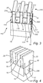
- Figure 1 shows, in perspective, a section of a substrate 10.
- the substrate 10 may extend laterally or horizontally beyond the illustrated section.
- the illustrated planes of section extending through the substrate 10 is common to all subsequent figures, unless stated otherwise. It is noted that the relative dimensions of the shown structures, for instance the relative thickness of layers, is merely schematic and may, for the purpose of illustrational clarity, differ from a physical structure.
- the indicated directions X, Y and Z refer to a first horizontal direction, a second horizontal direction and a vertical direction, respectively.
- the illustrated section of the substrate 10 may correspond to a section in which a functional cell is to be formed, such as a logic cell or a standard cell of a selected type. It will be appreciated that neighboring sections of the substrate 10 outside of the shown region may present a similarly structure and be processed in a corresponding manner as the illustrated section, in order to provide a plurality of similarly configured functional cells in parallel.
- the substrate 10 may be a conventional semiconductor substrate such as a silicon (Si) substrate, a germanium (Ge) substrate, a silicon germanium (SiGe) substrate, a silicon on insulator (SOI) substrate, a germanium on insulator (GeOI) substrate, or a SiGe on insulator (SiGeOI) substrate to name a few examples.
- a silicon (Si) substrate such as silicon (Si) substrate, a germanium (Ge) substrate, a silicon germanium (SiGe) substrate, a silicon on insulator (SOI) substrate, a germanium on insulator (GeOI) substrate, or a SiGe on insulator (SiGeOI) substrate to name a few examples.
- a first elongated semiconductor structure 100 and a second elongated semiconductor structure 200 extend in parallel to each other in a first horizontal direction X along the substrate 10 and protrude vertically above the substrate 10.
- the first semiconductor structure 100 and the second semiconductor structure 200 each have the shape of a respective semiconductor fin.
- the first semiconductor structure 100 and the second semiconductor structure 200 may therefore in the following be referred to as the first fin 100 and the second fin 200, respectively.
- Each fin 100, 200 may as shown have a top surface and two opposing sidewalls that protrude from the substrate 10.
- the fins 100, 200 may be formed by etching trenches in the substrate 10 or in a further semiconductor layer deposited on the substrate 10.
- the trenches may be formed using conventional patterning techniques such as single-patterning techniques, or multiple-patterning techniques, e.g. self-aligned double patterning (SADP) or quadruple patterning (SAQP).
- SADP self-aligned double patterning
- SAQP quadruple patterning
- a fin spacing may be on the order of a few tens of nm, such as about 10-50 nm.
- the first and second fins 100, 200 protrude above an insulating layer 12.
- the insulating layer 12 may e.g. be arranged in trenches on opposite sides of the respective fins 100, 200, and e.g. form a trench isolation or shallow trench isolation, STI.
- the first and the second fins 100, 200 may as shown have a same height above the substrate 10 and/or the insulating layer 12.
- a set of gate structures 14, 16, 18 has been formed to extend across the first fin 100 and the second fin 200.
- the gate structures 14, 16, 18 extend in a second horizontal direction Y. Regions of an upper portion of the first fin 100 (e.g. regions of the top surface of the first fin 100) disposed adjacent to and/or in between the gate structures 14, 16, 18 define a first set of regions 110 of the first fin 100. Regions of an upper portion of the second fin 200 (e.g. regions of the top surface of the second fin 200) disposed adjacent to and/or in between the gate structures 14, 16, 18 define a second set of regions 210 of the second fin 200.
- the first set of regions 110 include first regions 112, 114, 116, 118.
- the second set of regions 210 include second regions 212, 214, 216, 218. Each region may 112, 114, 116, 118 may form a source/drain region on the first fin 100. Each region may 212, 214, 216, 218 may form a source/drain region on the second fin 200. Although figure 2 shows three gate structures this is only an example and fewer gate structures (such as one or two) or more gate structures (such as four or five etc.) may be formed to extend across the first and second fins 100, 200.
- the gate structures 14, 16, 18 may be conductive gate structures (i.e. gate electrodes). Alternatively the gate structures 14, 16, 18 may be sacrificial gate structures intended to be replaced by final gate electrodes at a later stage. In any case the gate structures 14, 16, 18 may be formed by depositing a layer of gate material to cover the first and second fins 100, 200 and patterning the gate material layer to form the gate structures 14, 16, 18 as shown. In case the gate structures 14, 16, 18 are final gate electrodes, a gate dielectric may be present between the gate structures 14, 16, 18 and the fins 100, 200. Examples of conductive gate materials which may be used, include typical metals such as TiN, TaN, TiTaN, Al, TiAl, TiC, TiALC, or suitable combinations or stacks thereof. The metals may be deposited for instance by atomic layer deposition (ALD) or chemical vapor deposition (CVD). An example of a sacrificial gate material is polysilicon.
- ALD atomic layer deposition
- CVD chemical vapor deposition
- a respective gate cap 15 e.g. a hard mask material such as a nitride-based material for instance Si 3 N 4
- a respective gate cap 15 may remain on the gate structures 14, 16, 18 following the gate structure formation (e.g. gate mask 15 on the gate structure 14).
- a number of transistor devices may be formed along the first fin 100, the number depending on the number of gate structures 14, 16, 18.
- a number of transistor devices may be formed along the second fin 100.
- the regions 110 of the first fin 100 may form source/drain regions of the one or more transistor(s) along the first fin 100.
- the regions 210 of the first fin 200 may form source/drain regions of the one or more transistor(s) along the first fin 200.
- the region 124 and the region 126 may form a respective source/drain region of a first transistor along the first fin 100.
- the gate structure 16 may (possibly following a replacement metal gate process) form a gate of the first transistor.
- the region 224 and the region 226 may form a respective source/drain region of a second transistor along the second fin 200.
- the gate structure 16 may (possibly following a replacement metal gate process) form a gate of the second transistor.
- the first spacer layer 20 may, as it forms a sidewall spacer on the gate structures 14, 16, 18, also be referred to as a gate spacer layer 20.
- the first spacer layer 20 may as shown also cover the insulating layer 12.
- the first spacer layer 20 may be an oxide layer, for instance a silicon oxide carbide layer-based layer such as SiOC, SiBCN, SiOCN or SiOBCN.
- the first spacer layer 20 may also be formed by high-k dielectrics such as HfO 2 , ZrO 2 , AL 2 O 3 , to name a few.
- the first spacer layer 20 may be deposited by ALD.
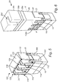
- an insulating layer 22 has been formed to embed the first and second fins 100, 200 and the gate structures 14, 16, 18.
- the insulating layer 22 may be formed by a dielectric material different from the first spacer layer 20.
- the insulating layer 22 may for instance be formed of a low-k dielectric material such as silicon oxide (SiO 2 ).
- the insulating layer 22 may be deposited by CVD.
- the insulating layer 22 may be deposited with a thickness to completely cover the gate structures 14, 16, 18.
- a planarization step may thereafter be performed, for instance by chemical mechanical polishing (CMP), to obtain a planarized insulating layer 22 exposing the gate caps 15.
- CMP chemical mechanical polishing
- a first set of source/drain contact openings 120 has been formed in the insulating layer 22.
- Each opening 122, 124, 126, 128 of the first set of source/drain contact openings 120 is formed above a respective region of the first set of regions 110.
- the opening 122 is formed above the region 112.
- the opening 124 is formed above the region 114.
- the opening 126 is formed above the region 116.
- the opening 128 is formed above the region 118.
- a first contact etch mask 24 is formed on the insulating layer 22.
- the etch mask 24 may be formed by a hard mask material, for instance a nitride-based material.
- An opening is formed in the first contact etch mask 24, e.g. by patterning the etch mask 24. The opening is formed to extend along the first fin 100, above each region 112, 114, 116, 118 of the first set of regions 110.
- the first set of source/drain contact openings 120 may thereafter be formed by etching the insulating layer 22 through the opening in the first contact etch mask 24.
- the etching may be a dry etch such as a reaction ion etch (RIE) or an ion beam etch (IBE).
- RIE reaction ion etch
- IBE ion beam etch
- the first set of source/drain contact openings 120 includes an opening 124, which in the following may be referred to as the first opening 124.
- the first opening 124 is formed above the region 114, which in the following may be referred to as the first region 114 (of the first fin 100).
- the first opening 124 has not yet been provided with its final form.
- the portion of the first opening 124 which has been formed may be referred to as the deep portion 124a of the first opening 124.
- a fill material layer 26 has been deposited to cover the first contact etch mask 24 and fill the deep portion 124a.
- the fill material layer 26 may for instance be a carbon-based material such as amorphous carbon (a-C) wherein the fill material layer 26 may be formed by spin-on deposition.
- the fill material layer 26 may however also be some other material which may fill the deep portion 124a, can be removed selectively to the insulating layer 22, and can be provided with a planar top surface.
- a second contact etch mask 28 has been formed on the fill material layer 26.
- the second contact etch mask 28 may be any type of single or composite etch mask being able to act as an etch mask during etching of the fill material layer 26, the first contact etch mask 24 and the insulating layer 22.
- the second etch mask 28 may as one example be a lithographic layer stack including a number of layers such as a silicon oxide nitride (SiON) layer 28a, a bottom antireflection coating (BARC) layer 28b and a resist layer 28c.
- An opening 28d has been formed in the resist layer 28c.
- the opening 28d is formed above a region of the insulating layer 22 adjacent to the deep portion 124a.
- the opening 28d may as shown extend also above the (filled) deep portion 124a.
- the opening 28d has been transferred into the lower layers of the second etch mask 28, e.g. layers 28b and 28a, to expose the fill material layer 26.
- the opening 28d has subsequently, in an etching process including a sequence of etching steps, been transferred into the fill material layer 26 and through a portion of the first contact etch mask 24 adjacent to the deep portion 124a to form an enlarged opening in the first contact etch mask 24, as shown in figure 7a .
- the insulating layer 22 has subsequently been etched through the enlarged opening in the first contact etch mask 24, selectively to the fill material layer 26 to form a shallow portion 124b.
- the deep portion 124a and the shallow portion 124b together define the completed first opening 124.
- the fill material layer 26 has subsequently been removed from the deep portion 124a, selectively to the etch mask 24 material and the insulating layer 22.
- Figure 7b shows in perspective a cross-sectional view taken along the line AA' indicated in figure 7a .
- the deep portion 124a is formed directly above the first region 114 of the first fin 100 and extends vertically through the insulating layer 22.
- a level V1 of a bottom surface 124ab of the deep portion 124a (formed by a remaining thickness portion of the insulating layer 22 under the deep portion 124a) is located below a level V2b of the first region 114.
- the level V2b may correspond to the level of the top surface of the fin 100.
- the region 114 of the fin 100 thus protrudes above the bottom surface 124ab.
- it is also possible to form the deep portion 124a such that the levels V1 and V2b coincide.
- the deep portion 124a such that the level V1 is located at or below a level V2a of the top surface of the first spacer layer portion 20 on the first region 114. This may still allow the first region 114 to be accessed by removing the top first spacer layer portion 20 at a later stage of the process.
- the shallow portion 124b is formed adjacent to the deep portion 124a and extends vertically through the insulating layer 22 such that a level V3 of a bottom surface 124bb of the shallow portion 124b (formed by a remaining thickness portion of the insulating layer 22 under the shallow portion 124b) is located above a level V4 of the region 214 of the second fin 200, which is directly opposite to the first region 114.
- the region 214 may in the following be referred to as the first region 214 (of the second fin 200).
- the level V4 corresponds to the level of the top surface of the fin 200.
- the deep portion 124a may be formed such that the level V1 of the bottom surface 124a is located above a level V9 (illustrated in figure 19c ) of the top semiconductor top portions.
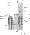
- Figure 7c shows in a plan view a part of the cross-section in figure 7a .
- the shallow portion 124b protrudes from the deep portion 124a in the second horizontal direction Y, towards the first region 214 of the second fin 200.
- the shallow portion 124b protrudes to, and optionally as shown slightly past, a horizontal position disposed halfway between the first fin 100 and the second fin 200.
- the openings 122, 126, 128 may each present corresponding bottom surfaces formed at a level at or below a level of the respective region 112, 116, 118 of the fin 100, or at or below a level of the top surface of the first spacer layer portion 20 on the respective region 112, 116, 118. More specifically, the openings 122, 126, 128 and the deep portion 124a may all be formed to present bottom surfaces located at a same level, e.g. level V1.
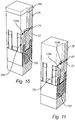
- Figures 8-11 show in greater detail a process sequence which may be performed to form the first contact opening including the deep portion 124a and the shallow portion 124b.
- Figure 8 shows in perspective a cross-sectional view taken along the line AA' through the structure at the stage reached in figure 6 .
- the fill material layer 26 has been etched through the opening 28d in the second contact etch mask 28 such that a portion 24a of the first contact etch mask 24 has been exposed.
- the etch mask 28 may as shown in figure 9 be partially consumed during the etching.
- the portion 24a is located above a region of the insulating layer 22 adjacent to the deep portion 124a.
- the portion 24a is the portion of the first contact etch mask 24 which covers the region of the insulating layer 22 in which the shallow portion 124b will be formed.
- the etching through the fill material layer 26 has been stopped while a portion 26a of the fill material layer 26 still remains in the deep portion 124a.
- the particular level of the top surface of the portion 26a merely is one example and that other levels are possible. At least, the portion 26a may however cover the bottom surface 124ab of the deep portion 124a.
- the portion 24a of the first contact etch mask 24 has been removed to expose the portion of the insulating layer 22 underneath.
- An enlarged opening has hence been formed in the first contact etch mask 24.
- the portion 24a may be removed by a short wet or dry etch step.
- the shallow portion 124b has been formed by etching the insulating layer 22 through the enlarged opening, selectively to the fill material layer portion 26a.
- a silicon oxide insulating layer 22 may be etched selectively from an a-C fill material layer portion 26a using a dry etch.
- the portion 26a is removed from the deep portion 124a by etching the portion 26a selectively to the insulating layer 22, thereby arriving at the structure shown in figures 7a-c . Also in this step, a dry etch may be employed.
- the first set of regions 110 have been exposed.
- the portions of the first spacer layer 20 covering the first set of regions 110, which portions are exposed in the first set of source/drain contact openings 120 have been removed.
- the portions may be removed by an anisotropic vertical etch, such as RIE.
- RIE anisotropic vertical etch
- Semiconductor top portions 113, 115, 117, 119 may then been grown in the first set of regions 110 to form doped source/drain regions 112, 114, 116, 118.
- the semiconductor material forming the top portions may be grown by selective epitaxy, for instance selective Si epitaxy or selective SiGe epitaxy.
- the grown semiconductor material may be doped with an n-type or p-type dopant, in accordance with the desired type of charge carriers for the transistor devices to be formed along the first fin 100.
- the semiconductor material may be doped by introducing appropriate impurities in the reaction chamber during the growth process.
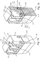
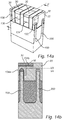
- a first set of source/drain contacts 130 has been formed in the first set of source/drain contact openings 120.
- a respective source/drain contact 132, 134, 136, 138 is formed in a respective one of the source/drain contact openings 122, 124, 126, 128.
- the top surfaces of the first set of contacts 130 are flush with the top surface of the insulating layer 22.
- Each of the first set of source/drain contacts 130 extends vertically through the insulating layer 22 into direct (physical and electrical) contact with a respective source/drain region 112, 114, 116, 118.
- the first set of source/drain contacts 130 includes the source/drain contact 134, which in the following may be referred to as the first source/drain contact 134 (of the first set of source/drain contacts 130).
- the first source/drain contact 134 is formed in the first source/drain contact opening 124.
- the first source/drain contact 134 includes a vertically extending contact portion 134a which is arranged in the deep portion 124a of the first source/drain contact opening 124.
- the contact portion 134a extends into direct (physical and electrical) contact with the (first) source/drain region 114.
- the first source/drain contact 134 includes a via landing portion 134b which is arranged in the shallow portion 124b of the first source/drain contact opening 124.
- the via landing portion 134b protrudes from the vertically extending contact portion 134a, in the second horizontal direction Y, towards the second fin 200. This may be seen also in figures 14a, 14b , where figure 14b shows in a plan view a cross-section taken along the line AA' indicated in figure 14a .
- the protruding via landing portion 134b extends at the level V3, above the level V4.
- the first set of source/drain contacts 130 have further been recessed, for instance by a suitable etch process allowing etching a metal source/drain contact material selectively to the insulating layer 22.
- the recesses have been filled with a capping layer 30.
- the capping layer may for instance be formed by depositing a SiC layer. Planarization has thereafter been performed to obtain separate capping layer portions, or contact caps 30, on each one of the first set of source/drain contacts 130.
- the first set of source/drain contacts 130 may be formed by depositing a conductive layer of one or more conductive materials in the first set of source/drain contact openings 120.
- a layer of metal such as Ti, TiN, WN, or an alloy of two or more thereof, may be deposited by ALD, CVD or physical vapor deposition (PVD).
- PVD physical vapor deposition
- a further layer of for instance W, Co, Ni, Ru or an alloy of two or more thereof, may be deposited on top of the first deposited conductive layer.
- the (single or composite) conductive layer may be deposited to completely fill the first set of source/drain contact openings 120 and cover upper surfaces of the insulating layer 22. Overburden conductive layer portions (i.e.
- conductive layer portions outside of the first set of source/drain contact openings 120 may thereafter be removed by CMP and/or etch back to expose the insulating layer 22, as shown in figure 13 . It is also possible to deposit the conductive layer to only partially fill the first set of source/drain contact openings 120 and thereafter planarize the structure to obtain a similar structure as in figure 13 with the top surfaces of the first set of contacts 130 flush with the top surface of the insulating layer 22.
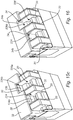
- FIG 15a a second set of source/drain contact openings 220 has been formed in the insulating layer 22.
- Figure 15b shows a cross section taken along the line BB' indicated in figure 15a .
- Each opening 222, 224, 226, 228 of the second set of source/drain contact openings 220 is formed above a respective region of the second set of regions 210.
- the opening 222 is formed above the region 212.
- the opening 224 is formed above the region 214, i.e. the region denoted "first region 214" above.
- the opening 226 is formed above the region 216.
- the opening 228 is formed above the region 218.
- the opening 226 of the second set of source/drain contact openings 220 may in the following be referred to as the second source/drain contact opening 226 (of the second set 220).
- the region 216 of the second set of regions 210 may correspondingly in the following be referred to as the second region 210 (of the second fin 200).
- the second source/drain contact opening 226 of the second set 220 is formed in a manner corresponding to the first source/drain contact opening 124 of the first set 120. More specifically, the second opening 226 includes a deep portion 226a and a shallow portion 226b.
- the deep portion 226a is formed directly above the second region 216 and extends vertically through the insulating layer 22 such that a level V5 of a bottom surface 226ab of the deep portion 226a (formed by a remaining thickness portion of the insulating layer 22 under the deep portion 226a) is located at or below a level V6b of the second region 216.
- the level V6b may correspond to the level of the top surface of the fin 200.
- the region 216 of the fin 200 thus protrudes above the bottom surface 226ab.
- the deep portion 226a such that the level V5 is located at or below a level V6a of the top surface of the first spacer layer portion 20 on the second region 216. This may still allow the second region 216 to be accessed by removing the top first spacer layer portion 20 at a later stage of the process.
- the shallow portion 226b is formed adjacent to the deep portion 226a and extends vertically through the insulating layer 22 such that a level V7 of a bottom surface 226bb of the shallow portion 226b (formed by a remaining thickness portion of the insulating layer 22 under the shallow portion 226b) is located above a level V8 of the directly opposite second region 116 of the first fin 100.
- the level V8 may as shown correspond to the level of the top of the semiconductor top portions. Otherwise the level V8 may correspond to the level of the top surface of the first fin 100.
- the shallow portion 226b protrudes from the deep portion 226a, in a third horizontal direction (opposite the second horizontal direction Y) towards the second region 116 of the first fin 100.
- the shallow portion 226b protrudes to, and optionally as shown slightly past, a horizontal position disposed halfway between the second fin 200 and the first fin 100.
- the openings 222, 224, 228 may each present corresponding bottom surfaces formed at a level at or below a level of the respective region 212, 214, 218 of the fin 200, or at or below a level of the top surface of the first spacer layer portion 20 on the respective region 212, 214, 218. More specifically, the openings 222, 224, 228 and the deep portion 226a may all be formed to present bottom surfaces located at a same level, e.g. level V5. The level V5 may coincide (at least approximately) with the level V1.
- the second set of source/drain contact openings 220 including the second source/drain contact opening 226 may be formed in a manner corresponding to the process steps described in connection with the forming of the first set of source/drain contact openings 120 and the first source/drain contact opening 124a, 124b. That is by forming an opening in a third contact etch mask 32, the opening extending along the second fin 200, above each region 212, 214, 216, 218 of the second set of regions 210, and thereafter etching of the insulating layer 22 through the opening.
- the shallow portion 226b may be formed adjacent to the deep portion 226a in a manner corresponding to the forming of the shallow portion 124b adjacent to the deep portion 124a.
- a fill material layer (corresponding to fill material layer 26) may be deposited to fill the deep portion 226a and cover the third contact etch mask 32.
- a fourth contact etch mask (corresponding to the second contact etch mask 28) formed on the fill material layer, a portion of the third contact etch mask 32 being formed above a region of the insulating layer 22 in which the shallow portion 226b is to be formed, may be removed by etching to form an enlarged opening in the third contact etch mask 32.
- the shallow portion 226b may thereafter be formed by etching the insulating layer 22 through the enlarged opening, selectively to the fill material layer portion.
- fill material in the deep portion 226a may be removed by etching the fill material selectively to the insulating layer 22.
- Figure 15c shows a slightly rotated view compared to figure 15a .
- the forming of the first source/drain contact opening 224 may result in an end portion of the protruding via landing portion 134b of the first source/drain contact 134 being exposed.
- the forming of the first source/drain contact opening 226, especially the shallow portion 226b thereof may result in the source/drain contact 136 of the first set of source/drain contacts 130 being exposed in the shallow portion 226b.
- a remaining thickness of the insulating layer 22 between the respective contacts and the contact openings 224 or 226 may still be too thin to ensure sufficient electrical insulation between the contacts 134, 136 and the source/drain contacts which are to be formed in the second set of source/drain contact openings 220.
- an insulating contact spacer layer 34 (or interchangeable a second spacer layer 34) may as shown in figure 16 be formed on the sidewalls of the second set of source/drain contact openings 220 prior to forming the second set of source/drain contacts 230 in the second set of source/drain contact openings 220.
- the portion 34b of the contact spacer layer 34 may provide (increased) insulation between the via landing portion 134b and the source/drain contact opening 224.
- the portion 34a of the contact spacer layer 34 may provide (increased) insulation between the source/drain contact 136 and the shallow portion 226b.
- the contact spacer layer 34 may be formed by depositing a conformal contact spacer layer covering exposed surfaces of the structure, for instance by ALD. An anisotropic vertical etch of the contact spacer layer may be performed to remove portions formed on horizontal surfaces such that the contact spacer layer 34 remains on the sidewalls in the second set of source/drain contact openings 220.
- the second set of regions 210 have been exposed.
- the portions of the first spacer layer 20 covering the second set of regions 210, which portions are exposed in the first set of source/drain contact openings 120 have been removed.
- portions of the contact spacer layer 34 covering the second set of regions 210 may also be removed if present.
- the portions may be removed by an anisotropic vertical etch, such as a RIE.
- semiconductor top portions 213, 215, 217, 219 may then be grown in the second set of regions 210, to form doped source/drain regions 212, 214, 216, 218.
- the portions may be formed in a similar manner as those formed in the first set of regions 110.
- a second set of source/drain contacts 230 has been formed in the second set of source/drain contact openings 220.
- the second set of contacts 230 may be formed in a manner corresponding to the first set of contacts 130 by depositing a conductive material in the second set of source/drain contact openings 220.
- a respective source/drain contact 232, 234, 236, 238 is formed in a respective one of the source/drain contact openings 222, 224, 226, 228.
- the top surfaces of the second set of contacts 130 are flush with the top surface of the insulating layer 22.
- Each of the second set of source/drain contacts 230 extends vertically through the insulating layer 22 into direct (physical and electrical) contact with a respective source/drain region 212, 214, 216, 218.
- the second set of source/drain contacts 230 includes the source/drain contact 236, which in the following may be referred to as the second source/drain contact 236 (of the second set of source/drain contacts 230).
- the second source/drain contact 236 is formed in the second source/drain contact opening 226.
- the second source/drain contact 236 includes a vertically extending contact portion 236a which is arranged in the deep portion 226a of the second source/drain contact opening 226.
- the contact portion 236a extends into direct (physical and electrical) contact with the (second) source/drain region 217.
- the second source/drain contact 236 includes a via landing portion 236b which is arranged in the shallow portion 226b of the second source/drain contact opening 226.
- the via landing portion 236b protrudes from the vertically extending contact portion 236a, in a horizontal direction towards the first fin 100.
- FIG. 19b shows a cross-section taken along the line BB' indicated in figure 19a .
- the portion 34b of the contact spacer layer 34 provides insulation between the source/drain contact 136 and the via landing portion 236b.
- Figure 19c shows a cross-section taken along the line AA' indicated in figure 19a .
- the portion 34b of the contact spacer layer 34 provides insulation between the source/drain contact 234 and the via landing portion 134b.
- the first region 114 of the first fin 100 and the second region 216 of the second fin 200 are regions formed on opposite sides of a same gate structure 16.
- the first region 114 and the second region 216 may also be separated by more than one gate structure.
- a contact corresponding to the contact 134 and including a vertically extending contact portion and a via landing portion may instead (or additionally) be formed above the region 112.
- a contact corresponding to the contact 236 and including a vertically extending contact portion and a via landing portion may instead (or additionally) be formed for instance above the region 218.
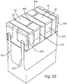
- Figures 20-22 show a variation of a process flow for forming a contact spacer layer in the second set of source/drain contact openings 220.
- the portions of the first spacer layer 20 formed on sidewalls of the gate structures 14, 16, 18 inside the second set of source/drain contact openings 220 are removed (see figure 20 ) prior to forming an insulating contact spacer layer 40 (interchangeably a second spacer layer 40) on the sidewalls of the source/drain contact openings 220 (see figure 21 ).
- the portions of the first spacer layer 20 may be removed by an isotropic etch. Any conventional wet etching chemistry allowing etching of the material forming the first spacer layer 20 may be used.
- the etching of the first spacer layer 20 may also result in removal of portions of the first spacer layer 20 formed on the fin 200, including the portions covering the second set of regions 210. As indicated in figure 21 , the etching of the first spacer layer 20 may result in a slight recess of the insulating layer 22.
- the contact spacer layer 40 may be formed in a corresponding manner as the contact spacer layer 34 and provides a corresponding function as the contact spacer layer 34. It could be made of a typical ALD dielectric, for instance SiO 2 , SiOC, SiOCN, SiBCN, SiON or SiN. However, as the first spacer layer 20 is removed from the sidewalls of the gate structures 14, 16, 18 prior to deposition of the contact spacer layer 40, a volume of the second set of contact openings may be reduced to a smaller extent than in the scenario in figure 16 .
- the portion 40b of the contact spacer layer 40 may provide (increased) insulation between the via landing portion 134b and the source/drain contact opening 224.
- the portion 40a of the contact spacer layer 40 may provide (increased) insulation between the source/drain contact 136 and the shallow portion 226b.
- the second set of source/drain contacts 230 has been formed in the second set of source/drain contact openings 220, following forming of the top portions 213, 215, 217, 219.
- a capping layer 42 has been formed on the second set of source/drain contacts 230 in a corresponding manner as the capping layer 30 disclosed above.
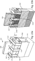
- an interconnection level 300 has been formed above the device level including the fins 100, 200, the gate structures 14, 16, 18 and the contacts 130, 230.
- Figure 23b shows a cross section along the line CC' indicated in figure 23a .
- the interconnection level 300 may be formed above either the structure shown in figure 19 or the structure shown in figure 22 .
- An interlayer dielectric embedding the interconnection level 300 has been omitted from the figure to allow a view of the structure.
- the interconnection level 300 includes a horizontal line or routing track 330 formed at a horizontal position halfway between the first and second fin 100, 200.
- a first vertical via 310 is formed to extend directly between the horizontal line 330 and the via landing portion 134b.
- a second vertical via 320 is formed to extend directly between the horizontal line 330 and the via landing portion 236b. Hence, a cross-coupling of the first source/drain contact 124 on the first fin 100 and the second source/drain contact 236 on the second fin 200 has been formed.
- the interconnection level 300 may be formed using conventional damascene style processing, such as a dual damascene process.
- a replacement metal gate process may be performed in a manner which per se is known in the art, to replace the set of sacrificial gate structures with a set of replacement gate structures 14, 16, 18.
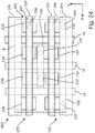
- Figure 24 is a schematic top-down view of a functional cell 400 including the first fin 100 and the second fin 200 with the respective sets of source/drain contacts 130, 230 formed thereon.
- the dashed line B indicates a cell boundary between the cell 400 and neighboring cells.
- the interconnection level 300 may, in addition to the routing track 330 forming a middle track of the cell 400, include routing tracks running parallel to the routing track 330.
- the interconnection level 300 may for instance include a routing track 332 formed at a horizontal position directly above the first fin 100.
- the interconnection level 300 may alternatively or additionally include a routing track 334 formed at a horizontal position directly above the second fin 200. These "off-center" routing tracks 332 and/or 334 may be tapped (i.e.
- routing tracks 332 and/or 334 may also be tapped to selected ones of the gate structures 14, 16, 18 in a corresponding manner.
- the interconnection level 300 may include a pair of edge routing tracks 331, 335 overlapping the cell boundary B on mutually opposite sides of the cell 400. By this arrangement, the edge routing tracks may be shared between neighboring cells.
- the edge routing tracks 331, 335 may for instance form power tracks for the cell 400 such as a VSS track and VDD track, respectively.
- the edge routing tracks 331, 335 may be tapped to selected ones of the source/drain contacts 130, 230. For instance, as shown, contacts 132, 138 and 238 may present a lateral extension such that the routing tracks 331, 335 extend directly above. The contacts 132, 138 and 238 may thus be connected to the routing tracks 331, 335 by a respective vertical via of the interconnection level 300, exemplified by via 338.
- the tracks 331, 332, 330, 334, 335 may be regularly spaced along the direction Y.
- the cell 400 has only three tracks available for internal routing. As may be understood, the exact configuration of the intra-cell routing, and connection points for the power rails will depend on the intended function of the functional cell 400.
- further interconnection levels may be formed above the interconnection level 300 and include routing tracks for instance for providing inter-cell routing, providing drive and gate voltages etc.
- first and second fin 100, 200 it should be noted that other configurations are possible for the first and second semiconductor structures 100, 200.
- each of the first and the second semiconductor structure 100, 200 may present, along at least a part of its length, a shape in the form of a set of horizontally extending nanowires or nanosheets arranged above each other and being suspended above the substrate 10.
- the suspended portions of the first and the second semiconductor structure 100, 200 may be tethered to non-suspended semiconductor portions below a first set of regions 110 and a second set of regions 210, which regions are discussed below.
- Such nanowire or nanosheet structures may be formed by etching away thickness portions of semiconductor fins, using techniques which per se are known.
- the nanowire and nanosheet portions may form transistor channel portions which allow the gate structures to wrap-around the channels.
Landscapes
- Insulated Gate Type Field-Effect Transistor (AREA)
- Semiconductor Memories (AREA)
- Metal-Oxide And Bipolar Metal-Oxide Semiconductor Integrated Circuits (AREA)
- Electrodes Of Semiconductors (AREA)
- Internal Circuitry In Semiconductor Integrated Circuit Devices (AREA)
Priority Applications (2)
| Application Number | Priority Date | Filing Date | Title |
|---|---|---|---|
| EP18152779.7A EP3514833B1 (fr) | 2018-01-22 | 2018-01-22 | Dispositif semi-conducteur et procédé |
| US16/253,321 US10833161B2 (en) | 2018-01-22 | 2019-01-22 | Semiconductor device and method |
Applications Claiming Priority (1)
| Application Number | Priority Date | Filing Date | Title |
|---|---|---|---|
| EP18152779.7A EP3514833B1 (fr) | 2018-01-22 | 2018-01-22 | Dispositif semi-conducteur et procédé |
Publications (2)
| Publication Number | Publication Date |
|---|---|
| EP3514833A1 true EP3514833A1 (fr) | 2019-07-24 |
| EP3514833B1 EP3514833B1 (fr) | 2022-05-11 |
Family
ID=61027465
Family Applications (1)
| Application Number | Title | Priority Date | Filing Date |
|---|---|---|---|
| EP18152779.7A Active EP3514833B1 (fr) | 2018-01-22 | 2018-01-22 | Dispositif semi-conducteur et procédé |
Country Status (2)
| Country | Link |
|---|---|
| US (1) | US10833161B2 (fr) |
| EP (1) | EP3514833B1 (fr) |
Cited By (1)
| Publication number | Priority date | Publication date | Assignee | Title |
|---|---|---|---|---|
| US20190229196A1 (en) * | 2018-01-22 | 2019-07-25 | Imec Vzw | Semiconductor Device and Method |
Families Citing this family (3)
| Publication number | Priority date | Publication date | Assignee | Title |
|---|---|---|---|---|
| KR20230026747A (ko) * | 2021-08-18 | 2023-02-27 | 삼성전자주식회사 | 반도체 장치 |
| EP4199052B1 (fr) * | 2021-12-17 | 2024-08-21 | IMEC vzw | Schéma de métallisation pour un circuit intégré |
| US20240213324A1 (en) * | 2022-12-22 | 2024-06-27 | Intel Corporation | Elongated contact for source or drain region |
Citations (2)
| Publication number | Priority date | Publication date | Assignee | Title |
|---|---|---|---|---|
| US20160056083A1 (en) * | 2014-08-25 | 2016-02-25 | Samsung Electronics Co., Ltd. | Method of manufacturing semiconductor devices |
| US20170229454A1 (en) * | 2016-02-10 | 2017-08-10 | Taiwan Semiconductor Manufacturing Co., Ltd. | Semiconductor device and a method for fabricating the same |
Family Cites Families (59)
| Publication number | Priority date | Publication date | Assignee | Title |
|---|---|---|---|---|
| KR102310122B1 (ko) | 2014-06-10 | 2021-10-08 | 삼성전자주식회사 | 논리 셀 및 이를 포함하는 집적회로 소자와 논리 셀의 제조 방법 및 집적회로 소자의 제조 방법 |
| US9589955B2 (en) * | 2014-10-01 | 2017-03-07 | Samsung Electronics Co., Ltd. | System on chip |
| CN105575885B (zh) * | 2014-10-14 | 2021-07-06 | 联华电子股份有限公司 | 半导体元件及其制作方法 |
| US9281379B1 (en) * | 2014-11-19 | 2016-03-08 | International Business Machines Corporation | Gate-all-around fin device |
| KR102340329B1 (ko) * | 2015-03-25 | 2021-12-21 | 삼성전자주식회사 | 반도체 소자 |
| KR102293185B1 (ko) * | 2015-04-21 | 2021-08-24 | 삼성전자주식회사 | 콘택 플러그들을 갖는 반도체 소자 및 그 형성 방법 |
| KR102366976B1 (ko) * | 2015-05-04 | 2022-02-24 | 삼성전자주식회사 | 콘택 플러그를 갖는 반도체 소자 및 그 형성 방법 |
| US9859210B2 (en) | 2015-06-19 | 2018-01-02 | Qualcomm Incorporated | Integrated circuits having reduced dimensions between components |
| US9923078B2 (en) * | 2015-10-30 | 2018-03-20 | International Business Machines Corporation | Trench silicide contacts with high selectivity process |
| US10497701B2 (en) * | 2015-12-16 | 2019-12-03 | Taiwan Semiconductor Manufacturing Co., Ltd. | Semiconductor device and manufacturing method thereof |
| US11088030B2 (en) * | 2015-12-30 | 2021-08-10 | Taiwan Semiconductor Manufacturing Co., Ltd. | Semiconductor device and a method for fabricating the same |
| US10466731B2 (en) * | 2016-01-27 | 2019-11-05 | Taiwan Semiconductor Manufacturing Co., Ltd. | Two-transistor bandgap reference circuit and FinFET device suited for same |
| US9947657B2 (en) * | 2016-01-29 | 2018-04-17 | Taiwan Semiconductor Manufacturing Co., Ltd. | Semiconductor device and a method for fabricating the same |
| US9741812B1 (en) * | 2016-02-24 | 2017-08-22 | International Business Machines Corporation | Dual metal interconnect structure |
| US9754822B1 (en) * | 2016-03-02 | 2017-09-05 | Taiwan Semiconductor Manufacturing Company, Ltd. | Interconnect structure and method |
| US9716158B1 (en) * | 2016-03-21 | 2017-07-25 | International Business Machines Corporation | Air gap spacer between contact and gate region |
| KR102481477B1 (ko) * | 2016-04-22 | 2022-12-26 | 삼성전자 주식회사 | 집적회로 소자 |
| KR102514620B1 (ko) * | 2016-04-28 | 2023-03-29 | 삼성전자주식회사 | 반도체 소자 및 이의 제조 방법 |
| US9893062B2 (en) * | 2016-04-28 | 2018-02-13 | Taiwan Semiconductor Manufacturing Co., Ltd. | Semiconductor device and a method for fabricating the same |
| US10276662B2 (en) * | 2016-05-31 | 2019-04-30 | Taiwan Semiconductor Manufacturing Co., Ltd. | Method of forming contact trench |
| US10115723B2 (en) * | 2016-06-03 | 2018-10-30 | Qualcomm Incorporated | Complementary metal oxide semiconductor (CMOS) devices employing plasma-doped source/drain structures and related methods |
| KR102524806B1 (ko) * | 2016-08-11 | 2023-04-25 | 삼성전자주식회사 | 콘택 구조체를 포함하는 반도체 소자 |
| US9741615B1 (en) * | 2016-08-22 | 2017-08-22 | Globalfoundries Inc. | Contacts for a fin-type field-effect transistor |
| US9929091B2 (en) * | 2016-08-25 | 2018-03-27 | International Business Machines Corporation | Vertical fuse structures |
| US10096604B2 (en) * | 2016-09-08 | 2018-10-09 | Globalfoundries Inc. | Selective SAC capping on fin field effect transistor structures and related methods |
| KR102575420B1 (ko) * | 2016-10-05 | 2023-09-06 | 삼성전자주식회사 | 반도체 장치 및 그 제조 방법 |
| US9837539B1 (en) * | 2016-11-29 | 2017-12-05 | Taiwan Semiconductor Manufacturing Company, Ltd. | FinFET device and method of forming |
| US10008497B2 (en) * | 2016-11-29 | 2018-06-26 | Taiwan Semiconductor Manufacturing Co., Ltd. | Method of manufacturing a semiconductor device and a semiconductor device |
| US9929157B1 (en) * | 2016-12-22 | 2018-03-27 | Globalfoundries Inc. | Tall single-fin fin-type field effect transistor structures and methods |
| KR102285271B1 (ko) * | 2017-04-03 | 2021-08-03 | 삼성전자주식회사 | 반도체 장치 |
| US10153198B2 (en) * | 2017-04-07 | 2018-12-11 | Taiwan Semiconductor Manufacturing Company, Ltd. | Low-resistance contact plugs and method forming same |
| US10453935B2 (en) * | 2017-04-20 | 2019-10-22 | International Business Machines Corporation | Thermally stable salicide formation for salicide first contacts |
| US9922882B1 (en) * | 2017-05-16 | 2018-03-20 | United Microelectronics Corp. | Manufacturing method of semiconductor structure |
| US10522392B2 (en) * | 2017-05-31 | 2019-12-31 | Taiwan Semiconductor Manufacturing Co., Ltd. | Semiconductor device and method of fabricating the same |
| US9911736B1 (en) * | 2017-06-14 | 2018-03-06 | Globalfoundries Inc. | Method of forming field effect transistors with replacement metal gates and contacts and resulting structure |
| KR102403031B1 (ko) * | 2017-10-19 | 2022-05-27 | 삼성전자주식회사 | 반도체 장치 |
| US10651284B2 (en) * | 2017-10-24 | 2020-05-12 | Globalfoundries Inc. | Methods of forming gate contact structures and cross-coupled contact structures for transistor devices |
| US10236215B1 (en) * | 2017-10-24 | 2019-03-19 | Globalfoundries Inc. | Methods of forming gate contact structures and cross-coupled contact structures for transistor devices |
| EP3514833B1 (fr) * | 2018-01-22 | 2022-05-11 | GLOBALFOUNDRIES U.S. Inc. | Dispositif semi-conducteur et procédé |
| US11031286B2 (en) * | 2018-03-01 | 2021-06-08 | Taiwan Semiconductor Manufacturing Co., Ltd. | Conductive feature formation and structure |
| KR102435522B1 (ko) * | 2018-03-27 | 2022-08-23 | 삼성전자주식회사 | 집적회로 장치 및 그 제조 방법 |
| US11227829B2 (en) * | 2018-03-29 | 2022-01-18 | Intel Corporation | Device terminal interconnect structures |
| KR102460847B1 (ko) * | 2018-05-25 | 2022-10-28 | 삼성전자주식회사 | 반도체 장치 및 그 제조 방법 |
| US11410928B2 (en) * | 2018-06-07 | 2022-08-09 | Intel Corporation | Device layer interconnects |
| US10770388B2 (en) * | 2018-06-15 | 2020-09-08 | International Business Machines Corporation | Transistor with recessed cross couple for gate contact over active region integration |
| US11244898B2 (en) * | 2018-06-29 | 2022-02-08 | Taiwan Semiconductor Manufacturing Co., Ltd | Integrated circuit interconnect structures with air gaps |
| US10658237B2 (en) * | 2018-07-31 | 2020-05-19 | Taiwan Semiconductor Manufacturing Co., Ltd. | Semiconductor devices |
| CN110875237B (zh) * | 2018-08-29 | 2021-12-14 | 中芯国际集成电路制造(上海)有限公司 | 半导体器件及其形成方法 |
| US11107810B2 (en) * | 2018-09-17 | 2021-08-31 | Taiwan Semiconductor Manufacturing Co., Ltd. | Fin field effect transistor (FinFET) device structure and method for forming the same |
| US11133254B2 (en) * | 2018-09-28 | 2021-09-28 | Taiwan Semiconductor Manufacturing Company, Ltd. | Hybrid power rail structure |
| US10672665B2 (en) * | 2018-09-28 | 2020-06-02 | Taiwan Semiconductor Manufacturing Co., Ltd. | Fin field effect transistor device structure and method for forming the same |
| US10741451B2 (en) * | 2018-10-03 | 2020-08-11 | Globalfoundries Inc. | FinFET having insulating layers between gate and source/drain contacts |
| US10804398B2 (en) * | 2018-10-15 | 2020-10-13 | Globalfoundries Inc. | Method of forming wrap-around-contact and the resulting device |
| US10818659B2 (en) * | 2018-10-16 | 2020-10-27 | Globalfoundries Inc. | FinFET having upper spacers adjacent gate and source/drain contacts |
| US10665590B2 (en) * | 2018-10-16 | 2020-05-26 | Globalfoundries Inc. | Wrap-around contact surrounding epitaxial regions of integrated circuit structures and method of forming same |
| US11063041B2 (en) * | 2018-10-31 | 2021-07-13 | Taiwan Semiconductor Manufacturing Co., Ltd. | Integrated circuit device including a power supply line and method of forming the same |
| US10867842B2 (en) * | 2018-10-31 | 2020-12-15 | Taiwan Semiconductor Manufacturing Company, Ltd. | Method for shrinking openings in forming integrated circuits |
| US10957604B2 (en) * | 2018-10-31 | 2021-03-23 | Taiwan Semiconductor Manufacturing Company, Ltd. | Semiconductor device and method |
| US10998238B2 (en) * | 2018-10-31 | 2021-05-04 | Taiwan Semiconductor Manufacturing Co., Ltd. | Integrated circuits with buried interconnect conductors |
-
2018
- 2018-01-22 EP EP18152779.7A patent/EP3514833B1/fr active Active
-
2019
- 2019-01-22 US US16/253,321 patent/US10833161B2/en active Active
Patent Citations (2)
| Publication number | Priority date | Publication date | Assignee | Title |
|---|---|---|---|---|
| US20160056083A1 (en) * | 2014-08-25 | 2016-02-25 | Samsung Electronics Co., Ltd. | Method of manufacturing semiconductor devices |
| US20170229454A1 (en) * | 2016-02-10 | 2017-08-10 | Taiwan Semiconductor Manufacturing Co., Ltd. | Semiconductor device and a method for fabricating the same |
Cited By (2)
| Publication number | Priority date | Publication date | Assignee | Title |
|---|---|---|---|---|
| US20190229196A1 (en) * | 2018-01-22 | 2019-07-25 | Imec Vzw | Semiconductor Device and Method |
| US10833161B2 (en) * | 2018-01-22 | 2020-11-10 | Imec Vzw | Semiconductor device and method |
Also Published As
| Publication number | Publication date |
|---|---|
| US10833161B2 (en) | 2020-11-10 |
| EP3514833B1 (fr) | 2022-05-11 |
| US20190229196A1 (en) | 2019-07-25 |
Similar Documents
| Publication | Publication Date | Title |
|---|---|---|
| CN109427775B (zh) | 集成电路及其形成方法 | |
| KR102575420B1 (ko) | 반도체 장치 및 그 제조 방법 | |
| US11557655B2 (en) | Device and method of forming with three-dimensional memory and three-dimensional logic | |
| CN112530861B (zh) | 制造半导体器件的方法 | |
| TW202109673A (zh) | 半導體裝置的形成方法 | |
| US20220238524A1 (en) | Complementary metal-oxide-semiconductor device and method of manufacturing the same | |
| US8932936B2 (en) | Method of forming a FinFET device | |
| US10833161B2 (en) | Semiconductor device and method | |
| US11646318B2 (en) | Connections from buried interconnects to device terminals in multiple stacked devices structures | |
| TW201839816A (zh) | 半導體裝置的形成方法 | |
| US20190348330A1 (en) | Structure and Formation Method of Semiconductor Device Structure | |
| US20240203994A1 (en) | Integrated Circuit Device and a Method for Forming the Same | |
| US20240274676A1 (en) | Semiconductor device including backside contact structure having low ohmic contact resistance | |
| TW202310405A (zh) | 半導體裝置結構 | |
| CN109300897B (zh) | 半导体装置及其制造方法 | |
| US11295977B2 (en) | Standard cell device and method of forming an interconnect structure for a standard cell device | |
| CN112420613B (zh) | 半导体器件及其形成方法 | |
| US20240204082A1 (en) | Method for Forming a Semiconductor Device | |
| US9929098B2 (en) | Copper via with barrier layer and cap layer | |
| EP4199113A1 (fr) | Procédé de formation d'une structure de dispositif à semiconducteur | |
| CN109244139B (zh) | 半导体装置及其制造方法 | |
| US20240204081A1 (en) | Method for forming a semiconductor device | |
| EP4379784B1 (fr) | Procédé de formation d'un dispositif à semi-conducteur comprenant un rail d'alimentation enterré | |
| US20260114036A1 (en) | Complementary field-effect transistor devices with self-aligned local interconnect and methods of forming | |
| US20250301704A1 (en) | Semiconductor device including gate-cut structure formed at early step of manufacturing process |
Legal Events
| Date | Code | Title | Description |
|---|---|---|---|
| PUAI | Public reference made under article 153(3) epc to a published international application that has entered the european phase |
Free format text: ORIGINAL CODE: 0009012 |
|
| STAA | Information on the status of an ep patent application or granted ep patent |
Free format text: STATUS: THE APPLICATION HAS BEEN PUBLISHED |
|
| AK | Designated contracting states |
Kind code of ref document: A1 Designated state(s): AL AT BE BG CH CY CZ DE DK EE ES FI FR GB GR HR HU IE IS IT LI LT LU LV MC MK MT NL NO PL PT RO RS SE SI SK SM TR |
|
| AX | Request for extension of the european patent |
Extension state: BA ME |
|
| STAA | Information on the status of an ep patent application or granted ep patent |
Free format text: STATUS: REQUEST FOR EXAMINATION WAS MADE |
|
| 17P | Request for examination filed |
Effective date: 20200123 |
|
| RBV | Designated contracting states (corrected) |
Designated state(s): AL AT BE BG CH CY CZ DE DK EE ES FI FR GB GR HR HU IE IS IT LI LT LU LV MC MK MT NL NO PL PT RO RS SE SI SK SM TR |
|
| RAP1 | Party data changed (applicant data changed or rights of an application transferred) |
Owner name: IMEC VZW Owner name: GLOBALFOUNDRIES U.S. INC. |
|
| GRAP | Despatch of communication of intention to grant a patent |
Free format text: ORIGINAL CODE: EPIDOSNIGR1 |
|
| STAA | Information on the status of an ep patent application or granted ep patent |
Free format text: STATUS: GRANT OF PATENT IS INTENDED |
|
| RIC1 | Information provided on ipc code assigned before grant |
Ipc: H01L 27/088 20060101ALI20211111BHEP Ipc: H01L 21/8234 20060101ALI20211111BHEP Ipc: H01L 29/78 20060101ALI20211111BHEP Ipc: H01L 29/417 20060101AFI20211111BHEP |
|
| INTG | Intention to grant announced |
Effective date: 20211213 |
|
| GRAS | Grant fee paid |
Free format text: ORIGINAL CODE: EPIDOSNIGR3 |
|
| GRAA | (expected) grant |
Free format text: ORIGINAL CODE: 0009210 |
|
| STAA | Information on the status of an ep patent application or granted ep patent |
Free format text: STATUS: THE PATENT HAS BEEN GRANTED |
|
| AK | Designated contracting states |
Kind code of ref document: B1 Designated state(s): AL AT BE BG CH CY CZ DE DK EE ES FI FR GB GR HR HU IE IS IT LI LT LU LV MC MK MT NL NO PL PT RO RS SE SI SK SM TR |
|
| REG | Reference to a national code |
Ref country code: GB Ref legal event code: FG4D |
|
| REG | Reference to a national code |
Ref country code: CH Ref legal event code: EP |
|
| REG | Reference to a national code |
Ref country code: AT Ref legal event code: REF Ref document number: 1492203 Country of ref document: AT Kind code of ref document: T Effective date: 20220515 |
|
| REG | Reference to a national code |
Ref country code: DE Ref legal event code: R096 Ref document number: 602018035237 Country of ref document: DE |
|
| REG | Reference to a national code |
Ref country code: IE Ref legal event code: FG4D |
|
| REG | Reference to a national code |
Ref country code: LT Ref legal event code: MG9D |
|
| REG | Reference to a national code |
Ref country code: NL Ref legal event code: MP Effective date: 20220511 |
|
| REG | Reference to a national code |
Ref country code: AT Ref legal event code: MK05 Ref document number: 1492203 Country of ref document: AT Kind code of ref document: T Effective date: 20220511 |
|
| PG25 | Lapsed in a contracting state [announced via postgrant information from national office to epo] |
Ref country code: SE Free format text: LAPSE BECAUSE OF FAILURE TO SUBMIT A TRANSLATION OF THE DESCRIPTION OR TO PAY THE FEE WITHIN THE PRESCRIBED TIME-LIMIT Effective date: 20220511 Ref country code: PT Free format text: LAPSE BECAUSE OF FAILURE TO SUBMIT A TRANSLATION OF THE DESCRIPTION OR TO PAY THE FEE WITHIN THE PRESCRIBED TIME-LIMIT Effective date: 20220912 Ref country code: NO Free format text: LAPSE BECAUSE OF FAILURE TO SUBMIT A TRANSLATION OF THE DESCRIPTION OR TO PAY THE FEE WITHIN THE PRESCRIBED TIME-LIMIT Effective date: 20220811 Ref country code: NL Free format text: LAPSE BECAUSE OF FAILURE TO SUBMIT A TRANSLATION OF THE DESCRIPTION OR TO PAY THE FEE WITHIN THE PRESCRIBED TIME-LIMIT Effective date: 20220511 Ref country code: LT Free format text: LAPSE BECAUSE OF FAILURE TO SUBMIT A TRANSLATION OF THE DESCRIPTION OR TO PAY THE FEE WITHIN THE PRESCRIBED TIME-LIMIT Effective date: 20220511 Ref country code: HR Free format text: LAPSE BECAUSE OF FAILURE TO SUBMIT A TRANSLATION OF THE DESCRIPTION OR TO PAY THE FEE WITHIN THE PRESCRIBED TIME-LIMIT Effective date: 20220511 Ref country code: GR Free format text: LAPSE BECAUSE OF FAILURE TO SUBMIT A TRANSLATION OF THE DESCRIPTION OR TO PAY THE FEE WITHIN THE PRESCRIBED TIME-LIMIT Effective date: 20220812 Ref country code: FI Free format text: LAPSE BECAUSE OF FAILURE TO SUBMIT A TRANSLATION OF THE DESCRIPTION OR TO PAY THE FEE WITHIN THE PRESCRIBED TIME-LIMIT Effective date: 20220511 Ref country code: ES Free format text: LAPSE BECAUSE OF FAILURE TO SUBMIT A TRANSLATION OF THE DESCRIPTION OR TO PAY THE FEE WITHIN THE PRESCRIBED TIME-LIMIT Effective date: 20220511 Ref country code: BG Free format text: LAPSE BECAUSE OF FAILURE TO SUBMIT A TRANSLATION OF THE DESCRIPTION OR TO PAY THE FEE WITHIN THE PRESCRIBED TIME-LIMIT Effective date: 20220811 Ref country code: AT Free format text: LAPSE BECAUSE OF FAILURE TO SUBMIT A TRANSLATION OF THE DESCRIPTION OR TO PAY THE FEE WITHIN THE PRESCRIBED TIME-LIMIT Effective date: 20220511 |
|
| PG25 | Lapsed in a contracting state [announced via postgrant information from national office to epo] |
Ref country code: RS Free format text: LAPSE BECAUSE OF FAILURE TO SUBMIT A TRANSLATION OF THE DESCRIPTION OR TO PAY THE FEE WITHIN THE PRESCRIBED TIME-LIMIT Effective date: 20220511 Ref country code: PL Free format text: LAPSE BECAUSE OF FAILURE TO SUBMIT A TRANSLATION OF THE DESCRIPTION OR TO PAY THE FEE WITHIN THE PRESCRIBED TIME-LIMIT Effective date: 20220511 Ref country code: LV Free format text: LAPSE BECAUSE OF FAILURE TO SUBMIT A TRANSLATION OF THE DESCRIPTION OR TO PAY THE FEE WITHIN THE PRESCRIBED TIME-LIMIT Effective date: 20220511 Ref country code: IS Free format text: LAPSE BECAUSE OF FAILURE TO SUBMIT A TRANSLATION OF THE DESCRIPTION OR TO PAY THE FEE WITHIN THE PRESCRIBED TIME-LIMIT Effective date: 20220911 |
|
| PG25 | Lapsed in a contracting state [announced via postgrant information from national office to epo] |
Ref country code: SM Free format text: LAPSE BECAUSE OF FAILURE TO SUBMIT A TRANSLATION OF THE DESCRIPTION OR TO PAY THE FEE WITHIN THE PRESCRIBED TIME-LIMIT Effective date: 20220511 Ref country code: SK Free format text: LAPSE BECAUSE OF FAILURE TO SUBMIT A TRANSLATION OF THE DESCRIPTION OR TO PAY THE FEE WITHIN THE PRESCRIBED TIME-LIMIT Effective date: 20220511 Ref country code: RO Free format text: LAPSE BECAUSE OF FAILURE TO SUBMIT A TRANSLATION OF THE DESCRIPTION OR TO PAY THE FEE WITHIN THE PRESCRIBED TIME-LIMIT Effective date: 20220511 Ref country code: EE Free format text: LAPSE BECAUSE OF FAILURE TO SUBMIT A TRANSLATION OF THE DESCRIPTION OR TO PAY THE FEE WITHIN THE PRESCRIBED TIME-LIMIT Effective date: 20220511 Ref country code: DK Free format text: LAPSE BECAUSE OF FAILURE TO SUBMIT A TRANSLATION OF THE DESCRIPTION OR TO PAY THE FEE WITHIN THE PRESCRIBED TIME-LIMIT Effective date: 20220511 Ref country code: CZ Free format text: LAPSE BECAUSE OF FAILURE TO SUBMIT A TRANSLATION OF THE DESCRIPTION OR TO PAY THE FEE WITHIN THE PRESCRIBED TIME-LIMIT Effective date: 20220511 |
|
| REG | Reference to a national code |
Ref country code: DE Ref legal event code: R097 Ref document number: 602018035237 Country of ref document: DE |
|
| PLBE | No opposition filed within time limit |
Free format text: ORIGINAL CODE: 0009261 |
|
| STAA | Information on the status of an ep patent application or granted ep patent |
Free format text: STATUS: NO OPPOSITION FILED WITHIN TIME LIMIT |
|
| PG25 | Lapsed in a contracting state [announced via postgrant information from national office to epo] |
Ref country code: AL Free format text: LAPSE BECAUSE OF FAILURE TO SUBMIT A TRANSLATION OF THE DESCRIPTION OR TO PAY THE FEE WITHIN THE PRESCRIBED TIME-LIMIT Effective date: 20220511 |
|
| 26N | No opposition filed |
Effective date: 20230214 |
|
| PG25 | Lapsed in a contracting state [announced via postgrant information from national office to epo] |
Ref country code: SI Free format text: LAPSE BECAUSE OF FAILURE TO SUBMIT A TRANSLATION OF THE DESCRIPTION OR TO PAY THE FEE WITHIN THE PRESCRIBED TIME-LIMIT Effective date: 20220511 |
|
| P01 | Opt-out of the competence of the unified patent court (upc) registered |
Effective date: 20230513 |
|
| REG | Reference to a national code |
Ref country code: CH Ref legal event code: PL |
|
| GBPC | Gb: european patent ceased through non-payment of renewal fee |
Effective date: 20230122 |
|
| PG25 | Lapsed in a contracting state [announced via postgrant information from national office to epo] |
Ref country code: LU Free format text: LAPSE BECAUSE OF NON-PAYMENT OF DUE FEES Effective date: 20230122 |
|
| REG | Reference to a national code |
Ref country code: BE Ref legal event code: MM Effective date: 20230131 |
|
| PG25 | Lapsed in a contracting state [announced via postgrant information from national office to epo] |
Ref country code: LI Free format text: LAPSE BECAUSE OF NON-PAYMENT OF DUE FEES Effective date: 20230131 Ref country code: GB Free format text: LAPSE BECAUSE OF NON-PAYMENT OF DUE FEES Effective date: 20230122 Ref country code: CH Free format text: LAPSE BECAUSE OF NON-PAYMENT OF DUE FEES Effective date: 20230131 |
|
| PG25 | Lapsed in a contracting state [announced via postgrant information from national office to epo] |
Ref country code: FR Free format text: LAPSE BECAUSE OF NON-PAYMENT OF DUE FEES Effective date: 20230131 Ref country code: BE Free format text: LAPSE BECAUSE OF NON-PAYMENT OF DUE FEES Effective date: 20230131 |
|
| PG25 | Lapsed in a contracting state [announced via postgrant information from national office to epo] |
Ref country code: IT Free format text: LAPSE BECAUSE OF FAILURE TO SUBMIT A TRANSLATION OF THE DESCRIPTION OR TO PAY THE FEE WITHIN THE PRESCRIBED TIME-LIMIT Effective date: 20220511 Ref country code: IE Free format text: LAPSE BECAUSE OF NON-PAYMENT OF DUE FEES Effective date: 20230122 |
|
| PG25 | Lapsed in a contracting state [announced via postgrant information from national office to epo] |
Ref country code: MC Free format text: LAPSE BECAUSE OF FAILURE TO SUBMIT A TRANSLATION OF THE DESCRIPTION OR TO PAY THE FEE WITHIN THE PRESCRIBED TIME-LIMIT Effective date: 20220511 |
|
| PG25 | Lapsed in a contracting state [announced via postgrant information from national office to epo] |
Ref country code: MC Free format text: LAPSE BECAUSE OF FAILURE TO SUBMIT A TRANSLATION OF THE DESCRIPTION OR TO PAY THE FEE WITHIN THE PRESCRIBED TIME-LIMIT Effective date: 20220511 |
|
| PG25 | Lapsed in a contracting state [announced via postgrant information from national office to epo] |
Ref country code: BG Free format text: LAPSE BECAUSE OF FAILURE TO SUBMIT A TRANSLATION OF THE DESCRIPTION OR TO PAY THE FEE WITHIN THE PRESCRIBED TIME-LIMIT Effective date: 20220511 |
|
| REG | Reference to a national code |
Ref country code: DE Ref legal event code: R079 Ref document number: 602018035237 Country of ref document: DE Free format text: PREVIOUS MAIN CLASS: H01L0029417000 Ipc: H10D0064230000 |
|
| PG25 | Lapsed in a contracting state [announced via postgrant information from national office to epo] |
Ref country code: BG Free format text: LAPSE BECAUSE OF FAILURE TO SUBMIT A TRANSLATION OF THE DESCRIPTION OR TO PAY THE FEE WITHIN THE PRESCRIBED TIME-LIMIT Effective date: 20220511 |
|
| PG25 | Lapsed in a contracting state [announced via postgrant information from national office to epo] |
Ref country code: CY Free format text: LAPSE BECAUSE OF FAILURE TO SUBMIT A TRANSLATION OF THE DESCRIPTION OR TO PAY THE FEE WITHIN THE PRESCRIBED TIME-LIMIT; INVALID AB INITIO Effective date: 20180122 |
|
| PG25 | Lapsed in a contracting state [announced via postgrant information from national office to epo] |
Ref country code: HU Free format text: LAPSE BECAUSE OF FAILURE TO SUBMIT A TRANSLATION OF THE DESCRIPTION OR TO PAY THE FEE WITHIN THE PRESCRIBED TIME-LIMIT; INVALID AB INITIO Effective date: 20180122 |
|
| PG25 | Lapsed in a contracting state [announced via postgrant information from national office to epo] |
Ref country code: TR Free format text: LAPSE BECAUSE OF FAILURE TO SUBMIT A TRANSLATION OF THE DESCRIPTION OR TO PAY THE FEE WITHIN THE PRESCRIBED TIME-LIMIT Effective date: 20220511 |
|
| PGFP | Annual fee paid to national office [announced via postgrant information from national office to epo] |
Ref country code: DE Payment date: 20251217 Year of fee payment: 9 |