EP3514845B1 - Indenocarbazolverbindung und organisches elektrolumineszentes element - Google Patents
Indenocarbazolverbindung und organisches elektrolumineszentes element Download PDFInfo
- Publication number
- EP3514845B1 EP3514845B1 EP17861864.1A EP17861864A EP3514845B1 EP 3514845 B1 EP3514845 B1 EP 3514845B1 EP 17861864 A EP17861864 A EP 17861864A EP 3514845 B1 EP3514845 B1 EP 3514845B1
- Authority
- EP
- European Patent Office
- Prior art keywords
- group
- compound
- indenocarbazole
- carbon atoms
- layer
- Prior art date
- Legal status (The legal status is an assumption and is not a legal conclusion. Google has not performed a legal analysis and makes no representation as to the accuracy of the status listed.)
- Active
Links
Images



Classifications
-
- H—ELECTRICITY
- H10—SEMICONDUCTOR DEVICES; ELECTRIC SOLID-STATE DEVICES NOT OTHERWISE PROVIDED FOR
- H10K—ORGANIC ELECTRIC SOLID-STATE DEVICES
- H10K85/00—Organic materials used in the body or electrodes of devices covered by this subclass
- H10K85/60—Organic compounds having low molecular weight
- H10K85/649—Aromatic compounds comprising a hetero atom
- H10K85/657—Polycyclic condensed heteroaromatic hydrocarbons
- H10K85/6574—Polycyclic condensed heteroaromatic hydrocarbons comprising only oxygen in the heteroaromatic polycondensed ring system, e.g. cumarine dyes
-
- C—CHEMISTRY; METALLURGY
- C07—ORGANIC CHEMISTRY
- C07D—HETEROCYCLIC COMPOUNDS
- C07D209/00—Heterocyclic compounds containing five-membered rings, condensed with other rings, with one nitrogen atom as the only ring hetero atom
- C07D209/56—Ring systems containing three or more rings
- C07D209/80—[b, c]- or [b, d]-condensed
- C07D209/94—[b, c]- or [b, d]-condensed containing carbocyclic rings other than six-membered
-
- C—CHEMISTRY; METALLURGY
- C07—ORGANIC CHEMISTRY
- C07D—HETEROCYCLIC COMPOUNDS
- C07D405/00—Heterocyclic compounds containing both one or more hetero rings having oxygen atoms as the only ring hetero atoms, and one or more rings having nitrogen as the only ring hetero atom
- C07D405/14—Heterocyclic compounds containing both one or more hetero rings having oxygen atoms as the only ring hetero atoms, and one or more rings having nitrogen as the only ring hetero atom containing three or more hetero rings
-
- C—CHEMISTRY; METALLURGY
- C09—DYES; PAINTS; POLISHES; NATURAL RESINS; ADHESIVES; COMPOSITIONS NOT OTHERWISE PROVIDED FOR; APPLICATIONS OF MATERIALS NOT OTHERWISE PROVIDED FOR
- C09K—MATERIALS FOR MISCELLANEOUS APPLICATIONS, NOT PROVIDED FOR ELSEWHERE
- C09K11/00—Luminescent materials, e.g. electroluminescent or chemiluminescent
- C09K11/06—Luminescent materials, e.g. electroluminescent or chemiluminescent containing organic luminescent materials
-
- H—ELECTRICITY
- H10—SEMICONDUCTOR DEVICES; ELECTRIC SOLID-STATE DEVICES NOT OTHERWISE PROVIDED FOR
- H10K—ORGANIC ELECTRIC SOLID-STATE DEVICES
- H10K50/00—Organic light-emitting devices
- H10K50/10—OLEDs or polymer light-emitting diodes [PLED]
- H10K50/18—Carrier blocking layers
- H10K50/181—Electron blocking layers
-
- H—ELECTRICITY
- H10—SEMICONDUCTOR DEVICES; ELECTRIC SOLID-STATE DEVICES NOT OTHERWISE PROVIDED FOR
- H10K—ORGANIC ELECTRIC SOLID-STATE DEVICES
- H10K50/00—Organic light-emitting devices
- H10K50/80—Constructional details
- H10K50/85—Arrangements for extracting light from the devices
-
- H—ELECTRICITY
- H10—SEMICONDUCTOR DEVICES; ELECTRIC SOLID-STATE DEVICES NOT OTHERWISE PROVIDED FOR
- H10K—ORGANIC ELECTRIC SOLID-STATE DEVICES
- H10K85/00—Organic materials used in the body or electrodes of devices covered by this subclass
- H10K85/60—Organic compounds having low molecular weight
- H10K85/649—Aromatic compounds comprising a hetero atom
- H10K85/657—Polycyclic condensed heteroaromatic hydrocarbons
- H10K85/6572—Polycyclic condensed heteroaromatic hydrocarbons comprising only nitrogen in the heteroaromatic polycondensed ring system, e.g. phenanthroline or carbazole
-
- C—CHEMISTRY; METALLURGY
- C07—ORGANIC CHEMISTRY
- C07D—HETEROCYCLIC COMPOUNDS
- C07D209/00—Heterocyclic compounds containing five-membered rings, condensed with other rings, with one nitrogen atom as the only ring hetero atom
- C07D209/56—Ring systems containing three or more rings
- C07D209/80—[b, c]- or [b, d]-condensed
- C07D209/82—Carbazoles; Hydrogenated carbazoles
- C07D209/86—Carbazoles; Hydrogenated carbazoles with only hydrogen atoms, hydrocarbon or substituted hydrocarbon radicals, directly attached to carbon atoms of the ring system
-
- C—CHEMISTRY; METALLURGY
- C09—DYES; PAINTS; POLISHES; NATURAL RESINS; ADHESIVES; COMPOSITIONS NOT OTHERWISE PROVIDED FOR; APPLICATIONS OF MATERIALS NOT OTHERWISE PROVIDED FOR
- C09K—MATERIALS FOR MISCELLANEOUS APPLICATIONS, NOT PROVIDED FOR ELSEWHERE
- C09K2211/00—Chemical nature of organic luminescent or tenebrescent compounds
- C09K2211/10—Non-macromolecular compounds
- C09K2211/1018—Heterocyclic compounds
- C09K2211/1025—Heterocyclic compounds characterised by ligands
-
- H—ELECTRICITY
- H10—SEMICONDUCTOR DEVICES; ELECTRIC SOLID-STATE DEVICES NOT OTHERWISE PROVIDED FOR
- H10K—ORGANIC ELECTRIC SOLID-STATE DEVICES
- H10K2101/00—Properties of the organic materials covered by group H10K85/00
- H10K2101/10—Triplet emission
-
- H—ELECTRICITY
- H10—SEMICONDUCTOR DEVICES; ELECTRIC SOLID-STATE DEVICES NOT OTHERWISE PROVIDED FOR
- H10K—ORGANIC ELECTRIC SOLID-STATE DEVICES
- H10K2101/00—Properties of the organic materials covered by group H10K85/00
- H10K2101/20—Delayed fluorescence emission
-
- H—ELECTRICITY
- H10—SEMICONDUCTOR DEVICES; ELECTRIC SOLID-STATE DEVICES NOT OTHERWISE PROVIDED FOR
- H10K—ORGANIC ELECTRIC SOLID-STATE DEVICES
- H10K50/00—Organic light-emitting devices
- H10K50/10—OLEDs or polymer light-emitting diodes [PLED]
- H10K50/11—OLEDs or polymer light-emitting diodes [PLED] characterised by the electroluminescent [EL] layers
-
- H—ELECTRICITY
- H10—SEMICONDUCTOR DEVICES; ELECTRIC SOLID-STATE DEVICES NOT OTHERWISE PROVIDED FOR
- H10K—ORGANIC ELECTRIC SOLID-STATE DEVICES
- H10K50/00—Organic light-emitting devices
- H10K50/10—OLEDs or polymer light-emitting diodes [PLED]
- H10K50/14—Carrier transporting layers
- H10K50/15—Hole transporting layers
-
- H—ELECTRICITY
- H10—SEMICONDUCTOR DEVICES; ELECTRIC SOLID-STATE DEVICES NOT OTHERWISE PROVIDED FOR
- H10K—ORGANIC ELECTRIC SOLID-STATE DEVICES
- H10K50/00—Organic light-emitting devices
- H10K50/10—OLEDs or polymer light-emitting diodes [PLED]
- H10K50/17—Carrier injection layers
-
- H—ELECTRICITY
- H10—SEMICONDUCTOR DEVICES; ELECTRIC SOLID-STATE DEVICES NOT OTHERWISE PROVIDED FOR
- H10K—ORGANIC ELECTRIC SOLID-STATE DEVICES
- H10K50/00—Organic light-emitting devices
- H10K50/10—OLEDs or polymer light-emitting diodes [PLED]
- H10K50/18—Carrier blocking layers
-
- H—ELECTRICITY
- H10—SEMICONDUCTOR DEVICES; ELECTRIC SOLID-STATE DEVICES NOT OTHERWISE PROVIDED FOR
- H10K—ORGANIC ELECTRIC SOLID-STATE DEVICES
- H10K71/00—Manufacture or treatment specially adapted for the organic devices covered by this subclass
- H10K71/10—Deposition of organic active material
- H10K71/12—Deposition of organic active material using liquid deposition, e.g. spin coating
-
- H—ELECTRICITY
- H10—SEMICONDUCTOR DEVICES; ELECTRIC SOLID-STATE DEVICES NOT OTHERWISE PROVIDED FOR
- H10K—ORGANIC ELECTRIC SOLID-STATE DEVICES
- H10K71/00—Manufacture or treatment specially adapted for the organic devices covered by this subclass
- H10K71/10—Deposition of organic active material
- H10K71/12—Deposition of organic active material using liquid deposition, e.g. spin coating
- H10K71/13—Deposition of organic active material using liquid deposition, e.g. spin coating using printing techniques, e.g. ink-jet printing or screen printing
- H10K71/135—Deposition of organic active material using liquid deposition, e.g. spin coating using printing techniques, e.g. ink-jet printing or screen printing using ink-jet printing
Definitions
- the present invention relates to the use of a compound suitable for an organic electroluminescence device (hereinafter, referred to as "organic EL device”) that is suitable for various display apparatuses and the organic EL device and more particularly to a specific indenocarbazole compound and an organic EL device using the compound.
- organic EL device an organic electroluminescence device
- An organic EL device is a self-light-emitting device, is brighter than a liquid crystal device, is excellent in visibility, and is capable of clearly displaying. For that reason, active studies have been made.
- a carrier is injected into a light-emitting material from both positive and negative electrodes, to thereby generating the light-emitting material in an excited state and emitting light.
- excitons excited to an excited singlet state are 25% of the excitons generated and the excitons excited to an excited triplet state are the rest, i.e., 75% of excitons generated. Accordingly, it appears that an energy utilization efficiency is higher when phosphorescence that emits light from the excited triplet state is used.
- a delayed fluorescent material showing delayed fluorescence.
- a certain fluorescent material emits fluorescence, after energy transition to the excited triplet state occurs by an intersystem crossing or the like, by triplet - triplet annihilation or by absorption of thermal energy through an inverse intersystem crossing to the excited singlet state.
- the latter i.e., a thermally activated delayed fluorescent material is believed to be particularly useful.
- the excitons in the excited singlet state emit normal fluorescence (immediate fluorescence).
- the excitons in the excited triplet state absorb heat generated from a device and emit delayed fluorescence through the inverse intersystem crossing to the excited singlet state.
- the delayed fluorescence is emitted from the excited singlet state, has the same wavelength as the immediate fluorescence, is generated through the inverse intersystem crossing from the excited triplet state to the excited singlet state, and has thus a longer light emission lifetime than the immediate fluorescence or the phosphorescence. Therefore, it is observed as fluorescence delayed slower than the immediate fluorescence or the phosphorescence.
- a high light-emitting efficiency can be provided by improving a probability of recombining holes and electrons by improving hole injecting properties into the light-emitting layer, improving electron blocking properties that block electrons injected from a cathode at an anode side of the light-emitting layer; and further by confining the excitons generated in the light-emitting layer.
- a hole transporting material having hole transporting properties that is used for forming a hole injecting layer, a hole transporting layer, an electron blocking layer, or the light-emitting layer plays an important role.
- the hole transporting material is required to have a great hole mobility, high hole injecting properties, great electron blocking properties, high triplet energy, and high durability to electrons.
- heat resistance and amorphousness of the material are important with respect to a device lifetime.
- the material having low heat resistance is thermally decomposed by heat generated at the time of driving the device even at a low temperature and is deteriorated. Further, in the material having low amorphousness, a thin film thereof is crystallized even in a short time, and the device is undesirably deteriorated. Accordingly, the materials used is required to have properties of high heat resistance and good amorphousness.
- NPD N,N'-diphenyl-N,N'-di ( ⁇ -naphthyl)benzidine
- Patent Literature 1 and Patent Literature 2 various aromatic amine derivatives have been known (Patent Literature 1 and Patent Literature 2).
- the NPD shows good hole transporting properties, but a low glass transition point (Tg) of as low as 96°C that is a heat-resistant indicator. Under a high temperature condition, device properties are lowered due to crystallization.
- Tg glass transition point
- some of aromatic amine derivatives described in Patent Literature 1 and Patent Literature 2 have excellent hole mobility of greater than 10- 3 cm 2 /Vs or more but have insufficient electron blocking properties.
- Patent Literature 3 As the compound having improved properties such as the heat resistance, the hole injecting properties, the hole transporting properties, and the electron blocking properties, an aromatic tertiary amine compound A represented by the following formula has been proposed (Patent Literature 3).
- Patent Literature 3 does not describe nor suggest the use of the delayed fluorescent material as the light-emitting material in the organic EL device using the compound.
- Patent Document 4 As a compound having electron transporting properties and hole transporting properties, an indenocarbazole derivative represented by the following formula (Y) has been proposed (Patent Document 4).
- the organic EL device in order to improve the device properties of the organic EL device, it is desirable to provide a material being excellent in the hole transporting properties, the hole injecting properties, the electron blocking properties, stability of a thin film state, and the like that can be used as the hole transporting material in the organic EL device.
- An object of the present invention is to use an indenocarbazole compound having (1) excellent hole transporting properties, (2) excellent electron blocking properties, (3) a stable thin film state, and excellent heat resistance as a material having hole transporting properties for formation of an organic EL device, in particular, to use said indenocarbazole compound for a constituent material of an electron blocking layer in a case where a delayed fluorescent material is used as the dopant material in a light-emitting layer.
- Another object of the present invention is to provide an organic EL device having a high light-emitting efficiency and high brightness.
- an indenocarbazole derivative having a specific structure according to claim 1 has the hole transporting properties, is excellent in the thin film stability and durability, and has high energy level in the lowest triplet state (T 1 ). Accordingly, the present inventors have designed and synthesized various indenocarbazole compounds and have intensively evaluated physical properties. As a result, it has discovered that an indenocarbazole compound has the excellent hole transporting properties, the excellent electron blocking properties, a stable thin film state, and excellent heat resistance.
- the present inventors have produced various organic EL devices by using the indenocarbazole compound and have intensively evaluated properties of the devices. As a result, the present invention has been accomplished.
- the present invention provides the use of an indenocarbazole compound with the features of claim 1, the indenocarbazole compound being represented by the following general formula (1).
- a preferred embodiment of the use of an indenocarbazole compound according to the present invention is as follows.
- an alkyl group having 1 to 8 carbon atoms, a cycloalkyl group having 5 to 10 carbon atoms, an alkenyl group having 2 to 6 carbon atoms, an alkyloxy group having 1 to 6 carbon atoms, a cycloalkyloxy group having 5 to 10 carbon atoms, an aromatic hydrocarbon group, an aromatic heterocyclic group, and aryloxy group represented by R 1 to R 12 may have a substituent, or may be unsubstituted.
- an aromatic hydrocarbon group or an aromatic heterocyclic group included in the disubstituted amino group as the substituent represented by R 1 to R 12 may have further a substituent, or may be unsubstituted.
- An aliphatic hydrocarbon group such as an alkyl group, an alkenyl group, and an alkyloxy group, unless otherwise specified, may be linear or branched.
- An aromatic hydrocarbon group and an aromatic heterocyclic group may have, unless otherwise specified, a single ring structure or a polycyclic structure, or further a condensed polycyclic structure.
- the organic electroluminescence device having a pair of electrodes and at least one organic layer sandwiched therebetween is characterized by the features of claim 4.
- the indenocarbazole compound according to the present invention has a high energy level of the lowest triplet state (T 1 ) and a wide band gap between the HOMO-LUMO. Therefore, it has hole transporting properties, and has one or more of the following properties.
- the thin-film state is stable and it is excellent in heat resistance. Because of such properties, the indenocarbazole compound according to the present invention is suitable as a material of the organic EL device. It is also possible to use as a material of an organic photoluminescence device.
- organic EL device according to the present invention using the indenocarbazole compound has the following properties:
- the indenocarbazole compound of claim 1 may be used as the material of the hole injecting layer or the hole transporting layer of the organic EL device.
- the organic EL device having the hole injecting layer or the hole transporting layer formed by using the indenocarbazole compound it is possible to confine the generated excitons in the emitting layer, increase a probability of recombining the holes and the electrons, and to obtain the high light-emitting efficiency. Also, the driving voltage is low and the durability is excellent.
- the indenocarbazole compound according to the present invention is used as a constituent material of the electron blocking layer of the organic EL device. This is because the indenocarbazole compound has the excellent electron blocking properties, the excellent hole transporting properties, and the stability of the thin film state is high.
- the organic EL device having the electron blocking layer produced by using the indenocarbazole compound according to the present invention has high light emission efficiency, a low driving voltage, excellent current resistance, high maximum light-emitting brightness.
- the indenocarbazole compound of claim 1 may be used as a material of the light-emitting layer of the organic EL device.
- the indenocarbazole compound has the excellent hole transporting properties and the wide band gap. Accordingly, by using the indenocarbazole compound as a host material of the light-emitting layer, causing to support a fluorescent light-emitting substance, a phosphorescence-emitting substance or a delayed fluorescent material which is called as a dopant, and forming the light-emitting layer, the organic EL device having the low driving voltage and the improved light-emitting efficiency is achievable.
- the organic EL device having improved various properties can be provided. Furthermore, by using the delayed fluorescence material in the light-emitting layer of the organic EL device according to the present invention as the dopant material, it is possible to avoid the use of the light-emitting material containing a rare metal such as iridium and platinum. In other words, expensive and scarce rare metals are not used and the indenocarbazole compound and the delayed fluorescence material are used in combination, the organic EL device according to the present invention advantageous in terms of resources and costs in addition to the above effects is achievable.
- the indenocarbazole compound according to the present invention is represented by the following general formula (1).
- the indenocarbazole compound represented by the general formula (1) includes an embodiment represented by the following general formula (1-1). This embodiment is the general formula (1) wherein binding positions of X, R 2 to R 9 , and R 12 are specified.
- R 1 represents a phenyl group, a diphenyl group, or a dibenzofuranyl group
- R 2 to R 12 may be the same or different and each represent a hydrogen atom; a deuterium atom; a fluorine atom; a chlorine atom; a cyano group; a nitro group; an alkyl group having 1 to 8 carbon atoms; a cycloalkyl group having 5 to 10 carbon atoms; an alkenyl group having 2 to 6 carbon atoms; an alkyloxy group having 1 to 6 carbon atoms; a cycloalkyloxy group having 5 to 10 carbon atoms; an aromatic hydrocarbon group; an aromatic heterocyclic group; an aryloxy group; or a disubstituted amino group substituted by a group selected from an aromatic hydrocarbon group or an aromatic heterocyclic group.
- R 1 to R 12 may be independently present and not to form a ring, but may bond each other via a single bond, a substituted or unsubstituted methylene group, an oxygen atom or a sulfur atom to form a ring. Note that in a case where R 1 to R 12 each is a disubstituted amino group, an aromatic hydrocarbon group or an aromatic heterocyclic group in the disubstituted amino group contributes to a ring formation.
- alkyl group having 1 to 8 carbon atoms examples include a methyl group, an ethyl group, an n-propyl group, an isopropyl group, an n-butyl group, an isobutyl group, a tert-butyl group, an n-pentyl group, an isopentyl group, a neopentyl group, an n-hexyl group, an n-octyl group; a cyclopentyl group, a cyclohexyl group, a 1-adamantyl group, a 2-adamantyl group, etc.; a vinyl group, an allyl group, a isopropenyl group, a 2-butenyl group; etc.
- alkyl group having 1 to 8 carbon atom examples include a methyl group, an ethyl group, an n-propyl group, an isopropyl group, an n-butyl group,
- the alkyl group having 1 to 8 carbon atoms, the cycloalkyl group having 5 to 10 carbon atoms or the alkenyl group having 2 to 6 carbon atoms represented by R 2 to R 12 may be unsubstituted however it is also suitable to have a substituent.
- substituents include the following groups in addition to a deuterium atom, a cyano group, and a nitro group:
- alkyloxy group having 1 to 6 carbon atoms or the cycloalkyloxy group having 5 to 10 carbon atoms represented by R 2 to R 12 include a methyloxy group, an ethyloxy group, an n-propyloxy group, an isopropyloxy group, an n-butyloxy group, a tert-butyloxy group, an n-pentyloxy group, an n-hexyloxy group, a cyclopentyloxy group, a cyclohexyloxy group, a cycloheptyloxy group, a cyclooctyloxy group, a 1-adamantyloxy group, a 2-adamantyloxy group.
- the alkyloxy group having 1 to 6 carbon atoms or the cycloalkyloxy group having 5 to 10 carbon atoms represented by R 2 to R 12 may be unsubstituted however it may also have a substituent.
- substituents include the same as those described with respect to the alkyl group having 1 to 8 carbon atoms, the cycloalkyl group having 5 to 10 carbon atoms, or the alkenyl group having 2 to 6 carbon atoms represented by R 2 to R 12 .
- the modes that can be taken are also the same.
- aromatic hydrocarbon group or the aromatic heterocyclic group represented by R 2 to R 12 include a phenyl group, a biphenylyl group, a terphenylyl group, a naphthyl group, an anthracenyl group, a phenanthrenyl group, a fluorenyl group, an indenyl group, a pyrenyl group, a perylenyl group, a fluoranthenyl group, a triphenylenyl group, a pyridyl group, a pyrimidinyl group, a triazinyl group, a furyl group, a pyrrolyl group, a thienyl group, a quinolyl group, an isoquinolyl group, a benzofuranyl group, a benzothienyl group, an indolyl group, a carbazolyl group, an indenocarbazolyl group, a benzoxazolyl
- the aromatic hydrocarbon group or the aromatic heterocyclic group represented by R 2 to R 12 may be unsubstituted or may have a substituent.
- substituents include the following groups in addition to a deuterium atom, a cyano group, and a nitro group:
- substituents may be unsubstituted, however may also be substituted with the above-described exemplified substituents. Further, these substituents may be independently present and not form a ring however may also bond each other via a single bond, a substituted or unsubstituted methylene group, an oxygen atom or a sulfur atom to form a ring.
- substituent is the disubstituted amino group, an alkyl group, an aromatic hydrocarbon group, an aralkyl group, an aromatic heterocyclic group or an alkenyl group constituting the disubstituted amino group contributes to a ring formation.
- aryloxy group represented by R 2 to R 12 include a phenyloxy group, biphenylyloxy group, a terphenyloxy group, a naphthyloxy group, an anthracenyloxy group, a phenanthrenyloxy group, a fluorenyloxy group, an indenyloxy group, a triphenylenyloxy group, a pyrenyloxy group, and a perylenyloxy group.
- the aromatic hydrocarbon group or the aromatic heterocyclic group represented by R 2 to R 12 may be unsubstituted however may also have a substituent.
- substituents include the same as those described with respect to the aromatic hydrocarbon group or the aromatic heterocyclic group represented by R 2 to R 12 .
- the embodiments that can be taken are also the same.
- Examples of the aromatic hydrocarbon group or the aromatic heterocyclic group of the substituent included in the disubstituted amino group represented by R 2 to R 12 include the same as those described with respect to the aromatic hydrocarbon group or the aromatic heterocyclic group represented by R 1 to R 12 .
- the aromatic hydrocarbon group or the aromatic heterocyclic group of the substituent included in the disubstituted amino group represented by R 2 to R 12 may be unsubstituted or may further have a substituent.
- substituent group include the same as those described with respect to the substituent that the aromatic hydrocarbon group or the aromatic heterocyclic group represented by R 2 to R 12 may have.
- the embodiments that can be taken are also the same.
- X represents an an unsubstituted carbazolyl group or an unsubstituted dibenzofuranyl group, and when X is an unsubstituted carbazolyl group, the nitrogen atom of the unsubstituted carbazolyl group is bonded to the indenocarbazole skeleton.
- the aromatic hydrocarbon group or the aromatic heterocyclic group of the substituent included in the disubstituted amino group represented by R 2 to R 12 may be unsubstituted or may further have a substituent.
- substituents include the same as those described with respect to the aromatic hydrocarbon group or the aromatic heterocyclic group represented by R 2 to R 12 .
- the embodiments that can be taken are also the same.
- the indenocarbazole compound is preferably the indenocarbazole compound represented by the general formula (1-1) .
- R 1 is a phenyl group, a biphenylyl group or a dibenzofuranyl group.
- the group represented by R 1 is preferably unsubstituted.
- R 2 to R 9 , and R 12 each is preferably a hydrogen atom or a deuterium atom, more preferably a hydrogen atom.
- R 10 and R 11 each is preferably an alkyl group or an aromatic hydrocarbon group having 1 to 8 carbon atoms, more preferably a methyl group, an octyl group or a phenyl group, particularly preferably a methyl group.
- X is an unsubstituted dibenzofuranyl group or an unsubstituted carbazolyl group, and when X is an unsubstituted carbazolyl group, the nitrogen atom of the unsubstituted carbazolyl group is bonded to the indenocarbazole skeleton. From the viewpoint of the device lifetime, an unsubstituted carbazolyl group is preferable. From the view point of the brightness, a light emission efficiency, and the power efficiency, an unsubstituted dibenzofuranyl group is preferable.
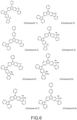
- indenocarbazole compound according to the present invention are compounds 2, 3, 7, 8, 24, 25 and 27 shown in Figs. 6 to 10 .
- the indenocarbazole compound is not limited to these compounds.
- D represents a deuterium atom.
- the indenocarbazole compound according to the present invention can be produced by known methods.
- the indenocarbazole compound can be synthesized by performing a condensation reaction such as the Buffubarudo-Hartwig reaction between indenocarbazole that is substituted with halogen such as bromine and amines such as a nitrogen-containing heterocyclic compound in the presence of a base.
- the indenocarbazole compound can be purified by column chromatograph purification, adsorption purification with silica gel, activated carbon, activated clay or the like, recrystallization or crystallization with a solvent, or the like. Also, the indenocarbazole compound may be purified by a sublimation purification method.
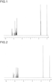
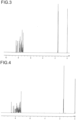
- the compound can be identified by an NMR analysis. As physical properties, a glass transition point (Tg), a work function, and the like can be measured.
- the glass transition point (Tg) is an index of the stability of the thin film state.
- the glass transition point (Tg) can be measured by a high sensitive differential scanning calorimeter (manufactured by Bruker AXS, DSC3100S) can be measured by using powder.
- the work function is an index of the hole transporting properties.
- the work function can be determined by preparing a thin film having a thickness of 100 nm on an ITO substrate and by using an ionization potential measuring apparatus (manufactured by Sumitomo Heavy Industries, Ltd., model PYS-202).
- the indenocarbazole compound according to the present invention has the hole transporting properties and shows the work function of 5.5 eV or more that is shown by a conventionally known hole transporting material such as NPD, TPD, and the like.
- the above-described indenocarbazole compound according to the present invention is used as a constituent material of the organic EL device.
- the indenocarbazole compound according to the present invention is used for a constituent material of an electron blocking layer.
- the organic EL device according to the present invention can take various embodiments of layer structures. For example, it is possible to take an embodiment in which only the light-emitting layer and the electron blocking layer are provided between the pair of electrodes. Alternatively, it is possible to take an embodiment in which the light-emitting layer, the electron blocking layer and other layer (hole injecting layer, hole transporting layer) are provided between the pair of electrodes.
- the electron blocking layer may be provided between the light-emitting layer and the hole transporting layer.
- a hole blocking layer may be provided between the light-emitting layer and the electron transporting layer.
- An exciton blocking layer may be provided on the light-emitting layer at an anode side or a cathode side.
- Fig. 5 shows a layer structure employed in the examples described below.
- a layer structure is shown by forming a transparent anode 2, a hole injecting layer 3, a hole transporting layer 4, an electron blocking layer 5, a light-emitting layer 6, a hole blocking layer 7, an electron transporting layer 8, an electron injecting layer 9, and a cathode 10 on a glass substrate 1 in this order.
- the anode 2 may be constituted per se by a known electrode material and an electrode material having a large work function such as ITO and gold is used, for example.
- the indenocarbazole compound according to claim 1 may be used for the hole injecting layer 3. Otherwise, known materials may be used for the hole injecting layer 3, or may be used by mixing or simultaneously with the indenocarbazole compound according to the present invention.
- Examples of the known materials include a porphyrin compound represented by copper phthalocyanine; a naphthalene diamine derivative; a starburst-type triphenylamine derivative; a triphenylamine trimer or tetramer having a structure that triphenylamines are single-bonded or linked by a divalent group containing no hetero atom; an acceptor-type heterocyclic compound such as hexacyano azatriphenylene; and a coating-type polymer material.
- a material to which tris-bromophenyl amine hexa chloro antimony, a radialene derivative ( WO 2014/009310 ), or the like is P-doped, a polymer compound having a partial structure including a structure of a benzidine derivative such as TPD, or the like can be used as well as the materials commonly used for the hole injecting layer.
- the hole injecting layer 3 can be provided by forming a thin film by any known method such as a vapor deposition method, a spin coating method, or an inkjet method by using these materials.
- the respective layers described below can be similarly provided by forming a thin film by any known method such as a vapor deposition method, a spin coating method, or an inkjet method.
- the indenocarbazole compound according to claim 1 may be also used for the hole transporting layer 4. Otherwise, known materials may be used for the hole transport layer 4, or may be used by mixing or simultaneously with the indenocarbazole compound according to the present invention.
- the hole transporting layer 4 may be formed by using the above-described materials alone, or may be formed by mixing with other materials.
- the hole transporting layer 4 may have a structure on which layers formed alone are laminated, layers formed by mixing are laminated, or a layer formed alone and a layer formed by mixing are laminated.
- Other organic layers in addition to the hole transporting layer may also have a similar structure.
- the hole injecting layer that also functions as the hole transporting layer can be formed by using the coating-type polymer materials such as poly(3,4-ethylenedioxythiophene) (PEDOT)/poly (styrene sulfonate) (PSS).
- PEDOT poly(3,4-ethylenedioxythiophene)
- PSS poly (styrene sulfonate)
- a material to which tris-bromophenyl amine hexa chloro antimony, a radialene derivative ( WO 2014/009310 ), or the like is P-doped, a polymer compound having a partial structure including a structure of a benzidine derivative such as TPD, or the like can be used as well as the materials commonly used for the hole transporting layer.
- the indenocarbazole compound according to claim 1 is used for the electron blocking layer 5.
- known compounds having an electron blocking effect may be used exemplified below, for example.
- Carbazole derivatives such as
- the indenocarbazole compound according to claim 1 may be also used for the light-emitting layer 6.
- known light-emitting materials may be used.
- the known light-emitting materials include a delayed fluorescent material including PIC-TRZ (see Non-Patent Literature 1), CC2TA (see Non-Patent Literature 2), PXZ-TRZ (see Non-Patent Literature 3), a carbazolyl dicyanobenzene (CDCB) derivative such 4CzIPN (see non-Patent Literature 4); various metal complexes such as a quinolinol derivative including tris(8-hydroxyquinoline)aluminum (Alq 3 ); a benzonitrile derivative; an anthracene derivative; a bis styryl benzene derivative; a pyrene derivative; an oxazole derivative; a polyparaphenylene vinylene derivative; and the like can be used.
- the organic EL device includes the light-emitting layer formed by using a heat activated delayed fluorescent material as a dopant material of the light-emitting layer, such that the organic EL device emits delayed fluorescence when current flows.
- the emitting layer 6 is preferably formed of the host material and the dopant material.
- a benzonitrile derivative mCP, mCBP, a thiazole derivative, a benzimidazole derivative, a polydialkylfluorene derivative, and the like can be used.
- the delayed fluorescent material including a benzonitrile derivative and a CDCB derivative such as PIC-TRZ, CC2TA, PXZ-TRZ, and 4CzIPN; quinacridone, coumarin, rubrene, anthracene, perylene and derivatives thereof; a benzopyran derivative; a rhodamine derivative; an aminostyryl derivative; and the like can be used.
- a benzonitrile derivative and a CDCB derivative such as PIC-TRZ, CC2TA, PXZ-TRZ, and 4CzIPN
- quinacridone coumarin, rubrene, anthracene, perylene and derivatives thereof
- a benzopyran derivative a rhodamine derivative
- an aminostyryl derivative and the like
- a phosphorescence-emitting substance as the light-emitting material.
- the phosphorescence-emitting substance include a metal complex of iridium or platinum. Specific examples include a green phosphorescence-emitting substance such as Ir(ppy) 3 ; a blue phosphorescence-emitting substance such as FIrpic and FIr6; and a red phosphorescence-emitting substance such as Btp 2 Ir(acac) and Ir(piq) 3 .
- the host material in this case, it is possible to use the indenocarbazole compound according to the present invention or a heterocyclic compound having an indole ring.
- Doping to the host material of the phosphorescence-emitting substance is preferably performed by co-vapor deposition in the range of 1 to 30% by weight with respect to the entire light-emitting layer in order to avoid concentration quenching.
- the light-emitting layer is formed using the heat activated delayed fluorescent material.
- any known compound having a hole blocking action can be used for the hole blocking layer 7.
- the known compound having a hole blocking action include a phenanthroline derivative such as bathocuproine (BCP); a metal complex of a quinolinol derivative such as aluminum (III)bis(2-methyl-8-quinolinato)-4-phenylphenolate (BAlq); a dibenzothiophene derivative such as 2,8-bis(diphenylphosphoryl)dibenzo[b, d]thiophene (PPT); a benzonitrile derivative; various rare earth complexes; an oxazole derivative; a triazole derivative; a triazine derivative; and the like. These materials may also serve as a material of the electron transporting layer.
- any known electron transporting material can be used for the electron transporting layer 8.
- the known electron transporting material include various metal complexes including a metal complex of a quinolinol derivative such as Alq 3 and BAlq; a triazole derivative; a benzonitrile derivative; a triazine derivative; an oxadiazole derivative; a pyridine derivative; a pyrimidine derivative; a thiadiazole derivative; a benzotriazole derivative; a carbodiimide derivative; a quinoxaline derivative; a pyridoindole derivative; a phenanthroline derivative; a silole derivative; a compound having an anthracene ring structure; a benzimidazole derivatives such as TPBI; and the like.
- a material to which metal such as cesium or a triarylphosphine oxide derivative ( WO 2014/195482 ) is N-doped can be used.
- an electron injecting layer 9 may be provided on the electron transporting layer 8.
- an alkali metal salt such as cesium fluoride and lithium fluoride; an alkaline earth metal salt such as magnesium fluoride; a metal oxide such as aluminum oxide; and the like can be used. It is possible to omit the electron injecting layer 9 by preferably selecting the electron transporting layer and the cathode.
- a material to which metal such as cesium or a triarylphosphine oxide derivative ( WO 2014/195482 ) is N-doped can be used.
- an electrode material having a low work function such as aluminum and an electrode material having a lower work function such as a magnesium-silver alloy, a magnesium-indium alloy, and an aluminum magnesium alloy are used.
- the high sensitivity differential scanning calorimeter (manufactured by Bruker AXS, DSC3100S) was used to determine the glass transition point of the compound obtained in each example.
- each of the indenocarbazole compounds according to the present invention had the glass transition temperature of 100°C or more and had a stable thin film state.
- a deposited film having a thickness of 100 nm was formed on an ITO substrate and was measured for the work function using the ionization potential measuring apparatus (manufactured by Sumitomo Heavy Industries, Ltd., PYS-202 type).
- each of the indenocarbazole compounds according to the present invention showed a preferable energy level and had good hole transportability as compared to the work function 5.5 eV of general hole transporting material such as NPD and TPD.
- the hole injecting layer 3 As shown in Fig. 5 , on the glass substrate 1 on which an ITO electrode was formed in advance as the transparent anode 2, the hole injecting layer 3, the hole transporting layer 4, the electron blocking layer 5, the light-emitting layer 6, the hole blocking layer 7, the electron transporting layer 8, the electron injecting layer 9, and the cathode (aluminum electrode) 10 were vapor-deposited in this order to produce an organic EL device that emits the delayed fluorescence.
- the glass substrate 1 on which ITO having a thickness of 150 nm was formed was washed with an organic solvent, the surface was cleaned by UV ozone treatment. After that, the glass substrate including the ITO electrode was mounted in a vacuum deposition apparatus, of which pressure was reduced to 0.001 Pa or less.
- a compound HIM-1 having the following formula was vapor-deposited so as to cover the transparent anode 2 to form the hole injecting layer 3 having a thickness of 10 nm.
- HTM-1 represented by the following structural formula was vapor-deposited to form the hole transporting layer 4 having a film thickness of 25 nm.
- the compound 1 of Example 1 was vapor-deposited to form the electron blocking layer 5 having a thickness of 5 nm.
- EMD-1 is a heat activated delayed fluorescent material.
- ETM-1 represented by the following structural formula was vapor-deposited to form the hole blocking layer 7 having a thickness of 10 nm.
- ETM-2 represented by the following structural formula was vapor-deposited to form the electron transporting layer 8 having a thickness of 40 nm.
- lithium fluoride was vapor-deposited to form the electron injecting layer 9 having a thickness of 1 nm.
- the organic EL devices produced in Device Examples 1 to 4 and Comparative Device Example 1 were measured for properties in the atmosphere at room temperature.
- Table 1 shows measurement results of light-emitting properties when a direct voltage is applied to each of the organic EL devices produced.
- the device lifetimes were measured by using organic EL devices produced in Device Examples 1 to 4 and Comparative Device Example 1. Specifically, when each device was driven with a constant current at light-emitting brightness (initial brightness) of 1000 cd/m 2 at the start of emitting light, the time to decay the light-emitting brightness to 950 cd/m 2 (corresponding to 95% of the initial brightness taking as 100%: 95% decay) was measured. Table 1 shows the results.
- Comparative Device Example 1 While the light-emitting efficiency of Comparative Device Example 1 was 46.6 cd/A, the light-emitting efficiencies of Device Examples 2 to 4 were high, i.e., 51.0 to 53.8 cd/A.
- Comparative Device Example 1 While the power efficiency of Comparative Device Example 1 was 27.0 lm/W, the power efficiencies of Device Examples 2 to 4 were similar thereto or more, i.e., 27.0 to 29.6 lm/W.
- Comparative Device Example 1 The device lifetime (95% decay) of Comparative Device Example 1 was 151 hours, which is the same with the device lifetime of Device Example 2.
- the organic EL device using the indenocarbazole compound according to claim 1 for the electron blocking layer and the heat activated delayed fluorescent material as the dopant material of the light-emitting layer had a high light-emitting efficiency and high brightness as compared with the known organic EL device using the HTM-A, and that a high power efficiency and a similar lifetime can be achieved depending on the structure of the indenocarbazole compound.
- Device Examples 2 and 3 having the electron blocking layers 5 formed by using the indenocarbazole compounds having the same structure other than R 1 in the formula (1) were compared.
- Device Example 2 using the compound 2 had the lifetime much longer than Device Example 3 using the compound 3, since the compound 2 had R 1 that was the phenyl group and the compound 3 had R 1 that was the biphenyl group.
- Device Examples 2 to 3 using the compounds 2 to 3 having X and R 1 not being the oxygen-containing aromatic heterocyclic group had the lifetime longer than Device Example 4 using the compound 24 having X and R 1 being the oxygen-containing aromatic heterocyclic groups.
- Device Example 4 had the brightness, the light-emitting efficiency, and the power efficiency better than Device Examples 2-3.
- the indenocarbazole compound according to the present invention has the hole transporting properties and is excellent in the electron blocking properties, and a thin film state is stable.
- the indenocarbazole compound according to the present invention is the excellent compound for the electron blocking layer of an organic EL device.
- the organic EL device according to the present invention produced using the compound has a high light-emitting efficiency and high brightness. Accordingly, the organic EL device according to the present invention can be applied to household electric appliances and lighting applications.
Landscapes
- Chemical & Material Sciences (AREA)
- Physics & Mathematics (AREA)
- Organic Chemistry (AREA)
- Optics & Photonics (AREA)
- Engineering & Computer Science (AREA)
- Materials Engineering (AREA)
- Spectroscopy & Molecular Physics (AREA)
- Electroluminescent Light Sources (AREA)
- Indole Compounds (AREA)
Claims (4)
- Verwendung einer Indenocarbazolverbindung mit Lochtransporteigenschaften als Bestandteil einer Elektronensperrschicht (5) einer organischen Elektrolumineszenzvorrichtung, die ein wärmeaktiviertes, verzögert fluoreszierendes Material als Dotierungsmaterial einer lichtemittierenden Schicht (6) enthält, wobei die Indenocarbazolverbindung durch die folgende allgemeine Formel (1) dargestellt wird
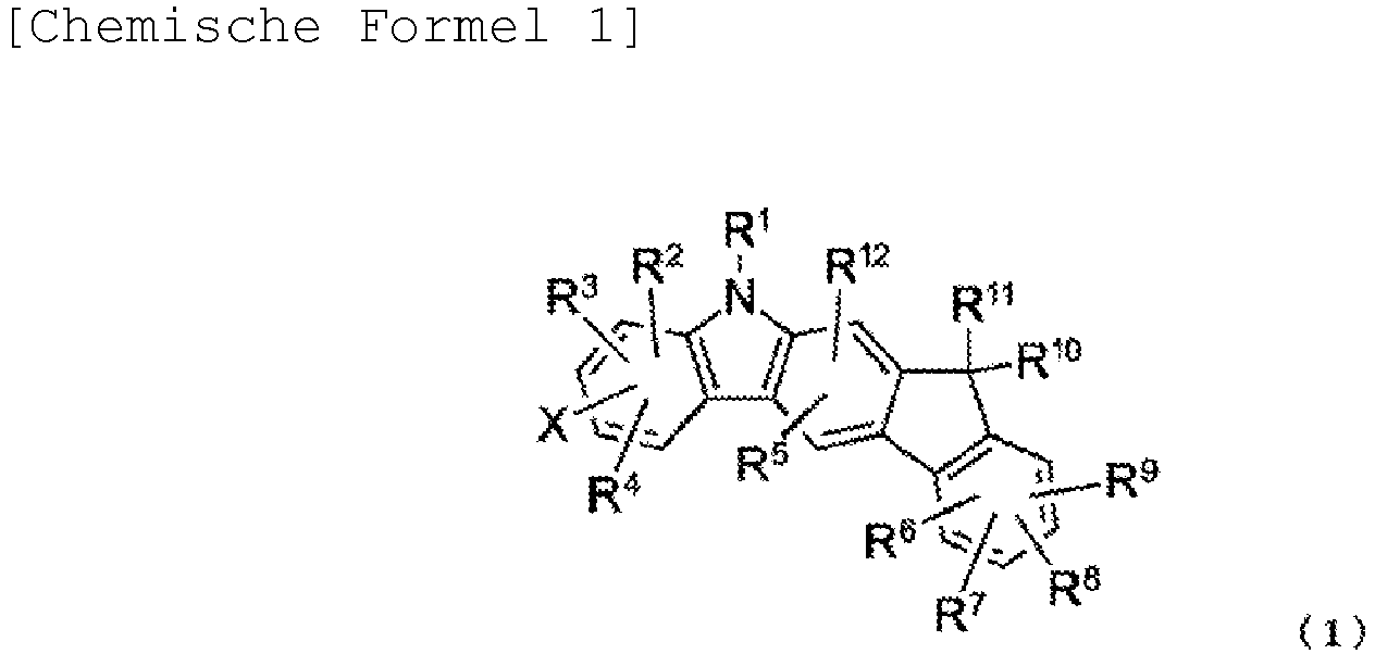 R1 eine Phenylgruppe, eine Diphenylgruppe oder eine Dibenzofuranylgruppe darstellt, R2 bis R12 gleich oder verschieden sein können und jeweils ein Wasserstoffatom; ein Deuteriumatom; ein Fluoratom; ein Chloratom; eine Cyanogruppe; eine Nitrogruppe; eine Alkylgruppe mit 1 bis 8 Kohlenstoffatomen; eine Cycloalkylgruppe mit 5 bis 10 Kohlenstoffatomen; eine Alkenylgruppe mit 2 bis 6 Kohlenstoffatomen; eine Alkyloxygruppe mit 1 bis 6 Kohlenstoffatomen eine Cycloalkyloxygruppe mit 5 bis 10 Kohlenstoffatomen; eine aromatische Kohlenwasserstoffgruppe; eine aromatische heterocyclische Gruppe; eine Aryloxygruppe; oder eine disubstituierte Aminogruppe, die mit einer aromatischen Kohlenwasserstoffgruppe oder einer aromatischen heterocyclischen Gruppe substituiert ist, wobei R1 bis R12 über eine Einfachbindung, eine substituierte oder unsubstituierte Methylengruppe, ein Sauerstoffatom oder ein Schwefelatom zu einem Ring verbunden sein können,X eine unsubstituierte Carbazolylgruppe oder eine unsubstituierte Dibenzofuranylgruppe darstellt, und wenn X eine unsubstituierte Carbazolylgruppe ist, das Stickstoffatom der unsubstituierten Carbazolylgruppe an das Indenocarbazolgerüst gebunden ist.
 - Verwendung nach Anspruch 1, wobei die Indenocarbazolverbindung durch die folgende allgemeine Formel (1-1) dargestellt wird

R1 bis R12 und X die in der allgemeinen Formel (1) beschriebene Bedeutung haben. - Verwendung nach Anspruch 1, wobei
die durch R2 bis R12 dargestellte Alkylgruppe mit 1 bis 8 Kohlenstoffatomen eine Alkylgruppe mit 1 bis 6 Kohlenstoffatomen ist. - Organische Elektrolumineszenzvorrichtung mit einem Paar von Elektroden (2, 10) und mindestens einer dazwischen angeordneten organischen Schicht, wobei die mindestens eine organische Schicht eine Elektronensperrschicht (5) umfasst, dieeine Indenocarbazolverbindung gemäß der allgemeinen Formel (1) von Anspruch 1 als Ausgangsmaterial hat; undeine lichtemittierende Schicht (6), die ein wärmeaktiviertes, verzögert fluoreszierendes Material als Dotierungsmaterial enthält.
Applications Claiming Priority (2)
| Application Number | Priority Date | Filing Date | Title |
|---|---|---|---|
| JP2016205109 | 2016-10-19 | ||
| PCT/JP2017/037746 WO2018074529A1 (ja) | 2016-10-19 | 2017-10-18 | インデノカルバゾール化合物および有機エレクトロルミネッセンス素子 |
Publications (3)
| Publication Number | Publication Date |
|---|---|
| EP3514845A1 EP3514845A1 (de) | 2019-07-24 |
| EP3514845A4 EP3514845A4 (de) | 2020-05-06 |
| EP3514845B1 true EP3514845B1 (de) | 2024-09-11 |
Family
ID=62018515
Family Applications (1)
| Application Number | Title | Priority Date | Filing Date |
|---|---|---|---|
| EP17861864.1A Active EP3514845B1 (de) | 2016-10-19 | 2017-10-18 | Indenocarbazolverbindung und organisches elektrolumineszentes element |
Country Status (7)
| Country | Link |
|---|---|
| US (1) | US11925114B2 (de) |
| EP (1) | EP3514845B1 (de) |
| JP (2) | JPWO2018074529A1 (de) |
| KR (1) | KR102491407B1 (de) |
| CN (1) | CN109844978B (de) |
| TW (1) | TWI741047B (de) |
| WO (1) | WO2018074529A1 (de) |
Families Citing this family (5)
| Publication number | Priority date | Publication date | Assignee | Title |
|---|---|---|---|---|
| EP3480192B1 (de) * | 2017-11-06 | 2020-12-23 | Novaled GmbH | Triazin verbindung und organische halbleitende schicht damit |
| KR20240022512A (ko) * | 2021-06-15 | 2024-02-20 | 가부시키가이샤 큐럭스 | 유기 발광 소자 및 그 제조 방법 |
| KR102884128B1 (ko) * | 2021-08-13 | 2025-11-13 | 국립한국교통대학교산학협력단 | 유기전계발광소자용 인데노카바졸계 고분자 화합물 및 이를 포함하는 유기전계발광소자 |
| CN113968811B (zh) * | 2021-11-16 | 2023-06-23 | 阜阳欣奕华材料科技有限公司 | 茚并咔唑类有机化合物及其应用 |
| WO2025205616A1 (ja) * | 2024-03-25 | 2025-10-02 | 保土谷化学工業株式会社 | 有機エレクトロルミネッセンス素子 |
Family Cites Families (29)
| Publication number | Priority date | Publication date | Assignee | Title |
|---|---|---|---|---|
| JP2004241374A (ja) | 2003-01-17 | 2004-08-26 | Sogo Pharmaceutical Co Ltd | 有機エレクトロルミネッセンス素子 |
| JP2006024830A (ja) | 2004-07-09 | 2006-01-26 | Sogo Pharmaceutical Co Ltd | 有機エレクトロルミネッセンス素子 |
| DE102009023155A1 (de) * | 2009-05-29 | 2010-12-02 | Merck Patent Gmbh | Materialien für organische Elektrolumineszenzvorrichtungen |
| JP5124785B2 (ja) * | 2009-12-07 | 2013-01-23 | 新日鉄住金化学株式会社 | 有機発光材料及び有機発光素子 |
| EP2599773B1 (de) | 2010-07-30 | 2017-03-29 | Hodogaya Chemical Co., Ltd. | Verbindung mit einer indencarbazol-ringstruktur und einem organischem elektrolumineszenzelement |
| CN103228647B (zh) * | 2010-11-24 | 2017-02-15 | 默克专利有限公司 | 用于有机电致发光器件的材料 |
| KR101947201B1 (ko) | 2011-02-28 | 2019-02-12 | 호도가야 가가쿠 고교 가부시키가이샤 | 유기 일렉트로루미네선스 소자 |
| EP2695213B1 (de) | 2011-04-05 | 2019-11-13 | Merck Patent GmbH | Organische elektrolumineszenzvorrichtung |
| KR102088637B1 (ko) * | 2011-07-29 | 2020-03-13 | 메르크 파텐트 게엠베하 | 전자 소자용 화합물 |
| KR101903216B1 (ko) | 2011-10-20 | 2018-10-01 | 메르크 파텐트 게엠베하 | 유기 전계발광 소자용 재료 |
| KR20130053846A (ko) | 2011-11-16 | 2013-05-24 | 롬엔드하스전자재료코리아유한회사 | 신규한 유기 발광 화합물 및 이를 채용하고 있는 유기 전계 발광 소자 |
| KR20130084093A (ko) * | 2012-01-16 | 2013-07-24 | 롬엔드하스전자재료코리아유한회사 | 신규한 유기 발광 화합물 및 이를 채용하고 있는 유기 전계 발광 소자 |
| KR20130118059A (ko) | 2012-04-19 | 2013-10-29 | 롬엔드하스전자재료코리아유한회사 | 신규한 유기 전계 발광 화합물 및 이를 사용하는 유기 전계 발광 소자 |
| EP2684932B8 (de) | 2012-07-09 | 2016-12-21 | Hodogaya Chemical Co., Ltd. | Diarylamino matrix material dotiert mit einer mesomeren radialenverbindung |
| JP6407883B2 (ja) * | 2012-12-14 | 2018-10-17 | メルク パテント ゲーエムベーハー | 電子素子のための材料 |
| WO2014112360A1 (ja) * | 2013-01-17 | 2014-07-24 | 保土谷化学工業株式会社 | インデノアクリダン環構造を有する化合物および有機エレクトロルミネッセンス素子 |
| CN105103328B (zh) | 2013-04-08 | 2018-06-05 | 默克专利有限公司 | 具有延迟荧光的有机发光器件 |
| JP6567498B2 (ja) * | 2013-04-08 | 2019-08-28 | メルク パテント ゲーエムベーハー | 熱活性化遅延蛍光材料をもつ有機エレクトロルミネッセント素子 |
| EP2811000B1 (de) | 2013-06-06 | 2017-12-13 | Novaled GmbH | Organische elektronische Vorrichtung |
| WO2014204464A1 (en) | 2013-06-20 | 2014-12-24 | Universal Display Corporation | Phosphorescent organic light emitting devices having a hole-transporting host in the emissive region |
| CN105636959B (zh) * | 2013-10-08 | 2019-10-18 | 默克专利有限公司 | 用于电子器件的材料 |
| EP3130015A1 (de) | 2014-04-11 | 2017-02-15 | Merck Patent GmbH | Materialien für organische elektrolumineszenzvorrichtungen |
| KR101790550B1 (ko) * | 2014-08-13 | 2017-10-26 | (주)피엔에이치테크 | 유기발광 화합물 및 이를 포함하는 유기전계발광소자 |
| US20180006237A1 (en) | 2015-01-30 | 2018-01-04 | Merck Patent Gmbh | Materials for electronic devices |
| WO2016186321A1 (en) | 2015-05-19 | 2016-11-24 | Rohm And Haas Electronic Materials Korea Ltd. | Phosphorous host material and organic electroluminescent device comprising the same |
| KR20160136211A (ko) * | 2015-05-19 | 2016-11-29 | 롬엔드하스전자재료코리아유한회사 | 인광 호스트 재료 및 이를 포함하는 유기 전계 발광 소자 |
| KR102740106B1 (ko) | 2016-03-03 | 2024-12-09 | 메르크 파텐트 게엠베하 | 유기 전계 발광 장치용 재료 |
| CN106467524B (zh) | 2016-07-29 | 2019-04-19 | 江苏三月光电科技有限公司 | 一种有机芳香化合物及其在有机电致发光器件上的应用 |
| CN106467484B (zh) | 2016-08-24 | 2020-04-03 | 中节能万润股份有限公司 | 一种以9-芴酮为核心的化合物及其在oled器件上的应用 |
-
2017
- 2017-10-18 WO PCT/JP2017/037746 patent/WO2018074529A1/ja not_active Ceased
- 2017-10-18 CN CN201780064324.3A patent/CN109844978B/zh active Active
- 2017-10-18 JP JP2018546390A patent/JPWO2018074529A1/ja active Pending
- 2017-10-18 US US16/342,410 patent/US11925114B2/en active Active
- 2017-10-18 EP EP17861864.1A patent/EP3514845B1/de active Active
- 2017-10-18 KR KR1020197013756A patent/KR102491407B1/ko active Active
- 2017-10-19 TW TW106135838A patent/TWI741047B/zh active
-
2021
- 2021-08-26 JP JP2021137690A patent/JP7217320B2/ja active Active
Also Published As
| Publication number | Publication date |
|---|---|
| JPWO2018074529A1 (ja) | 2019-08-29 |
| EP3514845A1 (de) | 2019-07-24 |
| JP2021192441A (ja) | 2021-12-16 |
| US20200058879A1 (en) | 2020-02-20 |
| KR20190065407A (ko) | 2019-06-11 |
| EP3514845A4 (de) | 2020-05-06 |
| CN109844978B (zh) | 2022-06-14 |
| CN109844978A (zh) | 2019-06-04 |
| KR102491407B1 (ko) | 2023-01-20 |
| JP7217320B2 (ja) | 2023-02-02 |
| TWI741047B (zh) | 2021-10-01 |
| US11925114B2 (en) | 2024-03-05 |
| WO2018074529A1 (ja) | 2018-04-26 |
| TW201827399A (zh) | 2018-08-01 |
Similar Documents
| Publication | Publication Date | Title |
|---|---|---|
| EP3275969B1 (de) | Material für ein organisches elektrolumineszenzelement, leuchtstoff und organisches elektrolumineszenzelement | |
| EP2960958B1 (de) | Organisches elektrolumineszenzelement | |
| EP3291323B1 (de) | Organisches elektrolumineszentes element | |
| EP3021372B1 (de) | Organisches elektrolumineszentes element | |
| KR102813012B1 (ko) | 트리아릴아민 구조를 갖는 화합물 및 유기 일렉트로 루미네선스 소자 | |
| EP2894155B1 (de) | Verbindung mit einer indenoacridanringstruktur und einem organischen elektrolumineszenzelement | |
| EP3370272A1 (de) | Organische elektrolumineszente vorrichtung | |
| WO2015136880A1 (ja) | アザフルオレン環構造を有するスピロ化合物、発光材料および有機エレクトロルミネッセンス素子 | |
| CN106573911A (zh) | 嘧啶衍生物和有机电致发光器件 | |
| EP3404735B1 (de) | Organisches elektrolumineszentes element | |
| EP3754739A1 (de) | Organisches elektrolumineszenzelement | |
| JP7217320B2 (ja) | 有機エレクトロルミネッセンス素子用材料及び有機エレクトロルミネッセンス素子 | |
| EP3544073A1 (de) | Organisches elektrolumineszenzelement | |
| JP6815320B2 (ja) | 有機エレクトロルミネッセンス素子 | |
| EP3605638B1 (de) | Organische elektrolumineszente vorrichtung | |
| CN110998889A (zh) | 含有具有苯并唑环结构的化合物的有机电致发光元件 | |
| KR102813014B1 (ko) | 아자벤조옥사졸 고리 구조를 갖는 화합물 및 유기 일렉트로루미네선스 소자 | |
| KR102705588B1 (ko) | 벤조이미다졸 고리 구조를 갖는 화합물 및 유기 일렉트로 루미네선스 소자 | |
| EP3890042A1 (de) | Organisches elektrolumineszentes element | |
| EP4050083B1 (de) | Organisches elektrolumineszentes element | |
| KR102931947B1 (ko) | 벤조트리아졸 고리 구조를 갖는 화합물 및 유기 일렉트로 루미네선스 소자 | |
| KR102817272B1 (ko) | 피리미딘 고리 구조를 갖는 화합물 및 유기 일렉트로 루미네선스 소자 | |
| JP2025156207A (ja) | 化合物、有機エレクトロルミネッセンス素子、および電子機器 |
Legal Events
| Date | Code | Title | Description |
|---|---|---|---|
| STAA | Information on the status of an ep patent application or granted ep patent |
Free format text: STATUS: THE INTERNATIONAL PUBLICATION HAS BEEN MADE |
|
| PUAI | Public reference made under article 153(3) epc to a published international application that has entered the european phase |
Free format text: ORIGINAL CODE: 0009012 |
|
| STAA | Information on the status of an ep patent application or granted ep patent |
Free format text: STATUS: REQUEST FOR EXAMINATION WAS MADE |
|
| 17P | Request for examination filed |
Effective date: 20190417 |
|
| AK | Designated contracting states |
Kind code of ref document: A1 Designated state(s): AL AT BE BG CH CY CZ DE DK EE ES FI FR GB GR HR HU IE IS IT LI LT LU LV MC MK MT NL NO PL PT RO RS SE SI SK SM TR |
|
| AX | Request for extension of the european patent |
Extension state: BA ME |
|
| DAV | Request for validation of the european patent (deleted) | ||
| DAX | Request for extension of the european patent (deleted) | ||
| A4 | Supplementary search report drawn up and despatched |
Effective date: 20200403 |
|
| RIC1 | Information provided on ipc code assigned before grant |
Ipc: H01L 51/54 20060101AFI20200330BHEP Ipc: C07D 209/86 20060101ALI20200330BHEP |
|
| STAA | Information on the status of an ep patent application or granted ep patent |
Free format text: STATUS: EXAMINATION IS IN PROGRESS |
|
| 17Q | First examination report despatched |
Effective date: 20211116 |
|
| REG | Reference to a national code |
Ref country code: DE Ref legal event code: R079 Free format text: PREVIOUS MAIN CLASS: H01L0051500000 Ipc: H10K0085600000 Ref country code: DE Ref legal event code: R079 Ref document number: 602017084834 Country of ref document: DE Free format text: PREVIOUS MAIN CLASS: H01L0051500000 Ipc: H10K0085600000 |
|
| RIC1 | Information provided on ipc code assigned before grant |
Ipc: H10K 101/20 20230101ALN20240306BHEP Ipc: H10K 50/18 20230101ALN20240306BHEP Ipc: C07D 209/86 20060101ALI20240306BHEP Ipc: H10K 85/60 20230101AFI20240306BHEP |
|
| GRAP | Despatch of communication of intention to grant a patent |
Free format text: ORIGINAL CODE: EPIDOSNIGR1 |
|
| STAA | Information on the status of an ep patent application or granted ep patent |
Free format text: STATUS: GRANT OF PATENT IS INTENDED |
|
| RIC1 | Information provided on ipc code assigned before grant |
Ipc: H10K 101/20 20230101ALN20240322BHEP Ipc: H10K 50/18 20230101ALN20240322BHEP Ipc: C07D 209/86 20060101ALI20240322BHEP Ipc: H10K 85/60 20230101AFI20240322BHEP |
|
| INTG | Intention to grant announced |
Effective date: 20240412 |
|
| P01 | Opt-out of the competence of the unified patent court (upc) registered |
Free format text: CASE NUMBER: APP_33711/2024 Effective date: 20240605 |
|
| GRAS | Grant fee paid |
Free format text: ORIGINAL CODE: EPIDOSNIGR3 |
|
| GRAA | (expected) grant |
Free format text: ORIGINAL CODE: 0009210 |
|
| STAA | Information on the status of an ep patent application or granted ep patent |
Free format text: STATUS: THE PATENT HAS BEEN GRANTED |
|
| AK | Designated contracting states |
Kind code of ref document: B1 Designated state(s): AL AT BE BG CH CY CZ DE DK EE ES FI FR GB GR HR HU IE IS IT LI LT LU LV MC MK MT NL NO PL PT RO RS SE SI SK SM TR |
|
| REG | Reference to a national code |
Ref country code: GB Ref legal event code: FG4D |
|
| REG | Reference to a national code |
Ref country code: CH Ref legal event code: EP |
|
| REG | Reference to a national code |
Ref country code: DE Ref legal event code: R096 Ref document number: 602017084834 Country of ref document: DE |
|
| REG | Reference to a national code |
Ref country code: IE Ref legal event code: FG4D |
|
| REG | Reference to a national code |
Ref country code: LT Ref legal event code: MG9D |
|
| PG25 | Lapsed in a contracting state [announced via postgrant information from national office to epo] |
Ref country code: NO Free format text: LAPSE BECAUSE OF FAILURE TO SUBMIT A TRANSLATION OF THE DESCRIPTION OR TO PAY THE FEE WITHIN THE PRESCRIBED TIME-LIMIT Effective date: 20241211 |
|
| REG | Reference to a national code |
Ref country code: NL Ref legal event code: MP Effective date: 20240911 |
|
| PG25 | Lapsed in a contracting state [announced via postgrant information from national office to epo] |
Ref country code: GR Free format text: LAPSE BECAUSE OF FAILURE TO SUBMIT A TRANSLATION OF THE DESCRIPTION OR TO PAY THE FEE WITHIN THE PRESCRIBED TIME-LIMIT Effective date: 20241212 Ref country code: FI Free format text: LAPSE BECAUSE OF FAILURE TO SUBMIT A TRANSLATION OF THE DESCRIPTION OR TO PAY THE FEE WITHIN THE PRESCRIBED TIME-LIMIT Effective date: 20240911 |
|
| PG25 | Lapsed in a contracting state [announced via postgrant information from national office to epo] |
Ref country code: BG Free format text: LAPSE BECAUSE OF FAILURE TO SUBMIT A TRANSLATION OF THE DESCRIPTION OR TO PAY THE FEE WITHIN THE PRESCRIBED TIME-LIMIT Effective date: 20240911 |
|
| PG25 | Lapsed in a contracting state [announced via postgrant information from national office to epo] |
Ref country code: LV Free format text: LAPSE BECAUSE OF FAILURE TO SUBMIT A TRANSLATION OF THE DESCRIPTION OR TO PAY THE FEE WITHIN THE PRESCRIBED TIME-LIMIT Effective date: 20240911 |
|
| PG25 | Lapsed in a contracting state [announced via postgrant information from national office to epo] |
Ref country code: HR Free format text: LAPSE BECAUSE OF FAILURE TO SUBMIT A TRANSLATION OF THE DESCRIPTION OR TO PAY THE FEE WITHIN THE PRESCRIBED TIME-LIMIT Effective date: 20240911 |
|
| PG25 | Lapsed in a contracting state [announced via postgrant information from national office to epo] |
Ref country code: RS Free format text: LAPSE BECAUSE OF FAILURE TO SUBMIT A TRANSLATION OF THE DESCRIPTION OR TO PAY THE FEE WITHIN THE PRESCRIBED TIME-LIMIT Effective date: 20241211 Ref country code: ES Free format text: LAPSE BECAUSE OF FAILURE TO SUBMIT A TRANSLATION OF THE DESCRIPTION OR TO PAY THE FEE WITHIN THE PRESCRIBED TIME-LIMIT Effective date: 20240911 |
|
| PG25 | Lapsed in a contracting state [announced via postgrant information from national office to epo] |
Ref country code: RS Free format text: LAPSE BECAUSE OF FAILURE TO SUBMIT A TRANSLATION OF THE DESCRIPTION OR TO PAY THE FEE WITHIN THE PRESCRIBED TIME-LIMIT Effective date: 20241211 Ref country code: NO Free format text: LAPSE BECAUSE OF FAILURE TO SUBMIT A TRANSLATION OF THE DESCRIPTION OR TO PAY THE FEE WITHIN THE PRESCRIBED TIME-LIMIT Effective date: 20241211 Ref country code: LV Free format text: LAPSE BECAUSE OF FAILURE TO SUBMIT A TRANSLATION OF THE DESCRIPTION OR TO PAY THE FEE WITHIN THE PRESCRIBED TIME-LIMIT Effective date: 20240911 Ref country code: HR Free format text: LAPSE BECAUSE OF FAILURE TO SUBMIT A TRANSLATION OF THE DESCRIPTION OR TO PAY THE FEE WITHIN THE PRESCRIBED TIME-LIMIT Effective date: 20240911 Ref country code: GR Free format text: LAPSE BECAUSE OF FAILURE TO SUBMIT A TRANSLATION OF THE DESCRIPTION OR TO PAY THE FEE WITHIN THE PRESCRIBED TIME-LIMIT Effective date: 20241212 Ref country code: FI Free format text: LAPSE BECAUSE OF FAILURE TO SUBMIT A TRANSLATION OF THE DESCRIPTION OR TO PAY THE FEE WITHIN THE PRESCRIBED TIME-LIMIT Effective date: 20240911 Ref country code: ES Free format text: LAPSE BECAUSE OF FAILURE TO SUBMIT A TRANSLATION OF THE DESCRIPTION OR TO PAY THE FEE WITHIN THE PRESCRIBED TIME-LIMIT Effective date: 20240911 Ref country code: BG Free format text: LAPSE BECAUSE OF FAILURE TO SUBMIT A TRANSLATION OF THE DESCRIPTION OR TO PAY THE FEE WITHIN THE PRESCRIBED TIME-LIMIT Effective date: 20240911 |
|
| REG | Reference to a national code |
Ref country code: AT Ref legal event code: MK05 Ref document number: 1723850 Country of ref document: AT Kind code of ref document: T Effective date: 20240911 |
|
| PG25 | Lapsed in a contracting state [announced via postgrant information from national office to epo] |
Ref country code: NL Free format text: LAPSE BECAUSE OF FAILURE TO SUBMIT A TRANSLATION OF THE DESCRIPTION OR TO PAY THE FEE WITHIN THE PRESCRIBED TIME-LIMIT Effective date: 20240911 |
|
| PG25 | Lapsed in a contracting state [announced via postgrant information from national office to epo] |
Ref country code: PT Free format text: LAPSE BECAUSE OF FAILURE TO SUBMIT A TRANSLATION OF THE DESCRIPTION OR TO PAY THE FEE WITHIN THE PRESCRIBED TIME-LIMIT Effective date: 20250113 Ref country code: IS Free format text: LAPSE BECAUSE OF FAILURE TO SUBMIT A TRANSLATION OF THE DESCRIPTION OR TO PAY THE FEE WITHIN THE PRESCRIBED TIME-LIMIT Effective date: 20250111 |
|
| PG25 | Lapsed in a contracting state [announced via postgrant information from national office to epo] |
Ref country code: SM Free format text: LAPSE BECAUSE OF FAILURE TO SUBMIT A TRANSLATION OF THE DESCRIPTION OR TO PAY THE FEE WITHIN THE PRESCRIBED TIME-LIMIT Effective date: 20240911 Ref country code: RO Free format text: LAPSE BECAUSE OF FAILURE TO SUBMIT A TRANSLATION OF THE DESCRIPTION OR TO PAY THE FEE WITHIN THE PRESCRIBED TIME-LIMIT Effective date: 20240911 |
|
| PG25 | Lapsed in a contracting state [announced via postgrant information from national office to epo] |
Ref country code: EE Free format text: LAPSE BECAUSE OF FAILURE TO SUBMIT A TRANSLATION OF THE DESCRIPTION OR TO PAY THE FEE WITHIN THE PRESCRIBED TIME-LIMIT Effective date: 20240911 Ref country code: AT Free format text: LAPSE BECAUSE OF FAILURE TO SUBMIT A TRANSLATION OF THE DESCRIPTION OR TO PAY THE FEE WITHIN THE PRESCRIBED TIME-LIMIT Effective date: 20240911 |
|
| PG25 | Lapsed in a contracting state [announced via postgrant information from national office to epo] |
Ref country code: CZ Free format text: LAPSE BECAUSE OF FAILURE TO SUBMIT A TRANSLATION OF THE DESCRIPTION OR TO PAY THE FEE WITHIN THE PRESCRIBED TIME-LIMIT Effective date: 20240911 Ref country code: PL Free format text: LAPSE BECAUSE OF FAILURE TO SUBMIT A TRANSLATION OF THE DESCRIPTION OR TO PAY THE FEE WITHIN THE PRESCRIBED TIME-LIMIT Effective date: 20240911 |
|
| PG25 | Lapsed in a contracting state [announced via postgrant information from national office to epo] |
Ref country code: SK Free format text: LAPSE BECAUSE OF FAILURE TO SUBMIT A TRANSLATION OF THE DESCRIPTION OR TO PAY THE FEE WITHIN THE PRESCRIBED TIME-LIMIT Effective date: 20240911 Ref country code: IT Free format text: LAPSE BECAUSE OF FAILURE TO SUBMIT A TRANSLATION OF THE DESCRIPTION OR TO PAY THE FEE WITHIN THE PRESCRIBED TIME-LIMIT Effective date: 20240911 |
|
| REG | Reference to a national code |
Ref country code: CH Ref legal event code: PL |
|
| REG | Reference to a national code |
Ref country code: DE Ref legal event code: R097 Ref document number: 602017084834 Country of ref document: DE |
|
| PG25 | Lapsed in a contracting state [announced via postgrant information from national office to epo] |
Ref country code: MC Free format text: LAPSE BECAUSE OF FAILURE TO SUBMIT A TRANSLATION OF THE DESCRIPTION OR TO PAY THE FEE WITHIN THE PRESCRIBED TIME-LIMIT Effective date: 20240911 |
|
| PG25 | Lapsed in a contracting state [announced via postgrant information from national office to epo] |
Ref country code: DK Free format text: LAPSE BECAUSE OF FAILURE TO SUBMIT A TRANSLATION OF THE DESCRIPTION OR TO PAY THE FEE WITHIN THE PRESCRIBED TIME-LIMIT Effective date: 20240911 |
|
| PG25 | Lapsed in a contracting state [announced via postgrant information from national office to epo] |
Ref country code: LU Free format text: LAPSE BECAUSE OF NON-PAYMENT OF DUE FEES Effective date: 20241018 Ref country code: BE Free format text: LAPSE BECAUSE OF NON-PAYMENT OF DUE FEES Effective date: 20241031 |
|
| PLBE | No opposition filed within time limit |
Free format text: ORIGINAL CODE: 0009261 |
|
| STAA | Information on the status of an ep patent application or granted ep patent |
Free format text: STATUS: NO OPPOSITION FILED WITHIN TIME LIMIT |
|
| PG25 | Lapsed in a contracting state [announced via postgrant information from national office to epo] |
Ref country code: CH Free format text: LAPSE BECAUSE OF NON-PAYMENT OF DUE FEES Effective date: 20241031 |
|
| REG | Reference to a national code |
Ref country code: BE Ref legal event code: MM Effective date: 20241031 |
|
| 26N | No opposition filed |
Effective date: 20250612 |
|
| GBPC | Gb: european patent ceased through non-payment of renewal fee |
Effective date: 20241211 |
|
| PG25 | Lapsed in a contracting state [announced via postgrant information from national office to epo] |
Ref country code: SE Free format text: LAPSE BECAUSE OF FAILURE TO SUBMIT A TRANSLATION OF THE DESCRIPTION OR TO PAY THE FEE WITHIN THE PRESCRIBED TIME-LIMIT Effective date: 20240911 |
|
| PG25 | Lapsed in a contracting state [announced via postgrant information from national office to epo] |
Ref country code: GB Free format text: LAPSE BECAUSE OF NON-PAYMENT OF DUE FEES Effective date: 20241211 |
|
| PG25 | Lapsed in a contracting state [announced via postgrant information from national office to epo] |
Ref country code: FR Free format text: LAPSE BECAUSE OF NON-PAYMENT OF DUE FEES Effective date: 20241111 |
|
| PG25 | Lapsed in a contracting state [announced via postgrant information from national office to epo] |
Ref country code: IE Free format text: LAPSE BECAUSE OF NON-PAYMENT OF DUE FEES Effective date: 20241018 |
|
| PGFP | Annual fee paid to national office [announced via postgrant information from national office to epo] |
Ref country code: DE Payment date: 20250902 Year of fee payment: 9 |
|
| PG25 | Lapsed in a contracting state [announced via postgrant information from national office to epo] |
Ref country code: CY Free format text: LAPSE BECAUSE OF FAILURE TO SUBMIT A TRANSLATION OF THE DESCRIPTION OR TO PAY THE FEE WITHIN THE PRESCRIBED TIME-LIMIT; INVALID AB INITIO Effective date: 20171018 |
|
| PG25 | Lapsed in a contracting state [announced via postgrant information from national office to epo] |
Ref country code: HU Free format text: LAPSE BECAUSE OF FAILURE TO SUBMIT A TRANSLATION OF THE DESCRIPTION OR TO PAY THE FEE WITHIN THE PRESCRIBED TIME-LIMIT; INVALID AB INITIO Effective date: 20171018 |