EP4050083B1 - Organisches elektrolumineszentes element - Google Patents
Organisches elektrolumineszentes element Download PDFInfo
- Publication number
- EP4050083B1 EP4050083B1 EP20878630.1A EP20878630A EP4050083B1 EP 4050083 B1 EP4050083 B1 EP 4050083B1 EP 20878630 A EP20878630 A EP 20878630A EP 4050083 B1 EP4050083 B1 EP 4050083B1
- Authority
- EP
- European Patent Office
- Prior art keywords
- group
- substituted
- unsubstituted
- substituent
- carbon atoms
- Prior art date
- Legal status (The legal status is an assumption and is not a legal conclusion. Google has not performed a legal analysis and makes no representation as to the accuracy of the status listed.)
- Active
Links
Images





Classifications
-
- C—CHEMISTRY; METALLURGY
- C09—DYES; PAINTS; POLISHES; NATURAL RESINS; ADHESIVES; COMPOSITIONS NOT OTHERWISE PROVIDED FOR; APPLICATIONS OF MATERIALS NOT OTHERWISE PROVIDED FOR
- C09K—MATERIALS FOR MISCELLANEOUS APPLICATIONS, NOT PROVIDED FOR ELSEWHERE
- C09K11/00—Luminescent materials, e.g. electroluminescent or chemiluminescent
- C09K11/06—Luminescent materials, e.g. electroluminescent or chemiluminescent containing organic luminescent materials
-
- C—CHEMISTRY; METALLURGY
- C07—ORGANIC CHEMISTRY
- C07B—GENERAL METHODS OF ORGANIC CHEMISTRY; APPARATUS THEREFOR
- C07B59/00—Introduction of isotopes of elements into organic compounds ; Labelled organic compounds per se
- C07B59/002—Heterocyclic compounds
-
- C—CHEMISTRY; METALLURGY
- C07—ORGANIC CHEMISTRY
- C07C—ACYCLIC OR CARBOCYCLIC COMPOUNDS
- C07C209/00—Preparation of compounds containing amino groups bound to a carbon skeleton
- C07C209/04—Preparation of compounds containing amino groups bound to a carbon skeleton by substitution of functional groups by amino groups
- C07C209/06—Preparation of compounds containing amino groups bound to a carbon skeleton by substitution of functional groups by amino groups by substitution of halogen atoms
- C07C209/10—Preparation of compounds containing amino groups bound to a carbon skeleton by substitution of functional groups by amino groups by substitution of halogen atoms with formation of amino groups bound to carbon atoms of six-membered aromatic rings or from amines having nitrogen atoms bound to carbon atoms of six-membered aromatic rings
-
- C—CHEMISTRY; METALLURGY
- C07—ORGANIC CHEMISTRY
- C07C—ACYCLIC OR CARBOCYCLIC COMPOUNDS
- C07C211/00—Compounds containing amino groups bound to a carbon skeleton
- C07C211/43—Compounds containing amino groups bound to a carbon skeleton having amino groups bound to carbon atoms of six-membered aromatic rings of the carbon skeleton
- C07C211/54—Compounds containing amino groups bound to a carbon skeleton having amino groups bound to carbon atoms of six-membered aromatic rings of the carbon skeleton having amino groups bound to two or three six-membered aromatic rings
-
- C—CHEMISTRY; METALLURGY
- C07—ORGANIC CHEMISTRY
- C07C—ACYCLIC OR CARBOCYCLIC COMPOUNDS
- C07C211/00—Compounds containing amino groups bound to a carbon skeleton
- C07C211/43—Compounds containing amino groups bound to a carbon skeleton having amino groups bound to carbon atoms of six-membered aromatic rings of the carbon skeleton
- C07C211/57—Compounds containing amino groups bound to a carbon skeleton having amino groups bound to carbon atoms of six-membered aromatic rings of the carbon skeleton having amino groups bound to carbon atoms of six-membered aromatic rings being part of condensed ring systems of the carbon skeleton
- C07C211/58—Naphthylamines; N-substituted derivatives thereof
-
- C—CHEMISTRY; METALLURGY
- C07—ORGANIC CHEMISTRY
- C07F—ACYCLIC, CARBOCYCLIC OR HETEROCYCLIC COMPOUNDS CONTAINING ELEMENTS OTHER THAN CARBON, HYDROGEN, HALOGEN, OXYGEN, NITROGEN, SULFUR, SELENIUM OR TELLURIUM
- C07F5/00—Compounds containing elements of Groups 3 or 13 of the Periodic Table
- C07F5/02—Boron compounds
-
- C—CHEMISTRY; METALLURGY
- C07—ORGANIC CHEMISTRY
- C07F—ACYCLIC, CARBOCYCLIC OR HETEROCYCLIC COMPOUNDS CONTAINING ELEMENTS OTHER THAN CARBON, HYDROGEN, HALOGEN, OXYGEN, NITROGEN, SULFUR, SELENIUM OR TELLURIUM
- C07F5/00—Compounds containing elements of Groups 3 or 13 of the Periodic Table
- C07F5/02—Boron compounds
- C07F5/027—Organoboranes and organoborohydrides
-
- H—ELECTRICITY
- H10—SEMICONDUCTOR DEVICES; ELECTRIC SOLID-STATE DEVICES NOT OTHERWISE PROVIDED FOR
- H10K—ORGANIC ELECTRIC SOLID-STATE DEVICES
- H10K50/00—Organic light-emitting devices
- H10K50/10—OLEDs or polymer light-emitting diodes [PLED]
- H10K50/11—OLEDs or polymer light-emitting diodes [PLED] characterised by the electroluminescent [EL] layers
- H10K50/12—OLEDs or polymer light-emitting diodes [PLED] characterised by the electroluminescent [EL] layers comprising dopants
-
- H—ELECTRICITY
- H10—SEMICONDUCTOR DEVICES; ELECTRIC SOLID-STATE DEVICES NOT OTHERWISE PROVIDED FOR
- H10K—ORGANIC ELECTRIC SOLID-STATE DEVICES
- H10K85/00—Organic materials used in the body or electrodes of devices covered by this subclass
- H10K85/30—Coordination compounds
- H10K85/321—Metal complexes comprising a group IIIA element, e.g. Tris (8-hydroxyquinoline) gallium [Gaq3]
- H10K85/322—Metal complexes comprising a group IIIA element, e.g. Tris (8-hydroxyquinoline) gallium [Gaq3] comprising boron
-
- H—ELECTRICITY
- H10—SEMICONDUCTOR DEVICES; ELECTRIC SOLID-STATE DEVICES NOT OTHERWISE PROVIDED FOR
- H10K—ORGANIC ELECTRIC SOLID-STATE DEVICES
- H10K85/00—Organic materials used in the body or electrodes of devices covered by this subclass
- H10K85/60—Organic compounds having low molecular weight
- H10K85/631—Amine compounds having at least two aryl rest on at least one amine-nitrogen atom, e.g. triphenylamine
-
- H—ELECTRICITY
- H10—SEMICONDUCTOR DEVICES; ELECTRIC SOLID-STATE DEVICES NOT OTHERWISE PROVIDED FOR
- H10K—ORGANIC ELECTRIC SOLID-STATE DEVICES
- H10K85/00—Organic materials used in the body or electrodes of devices covered by this subclass
- H10K85/60—Organic compounds having low molecular weight
- H10K85/631—Amine compounds having at least two aryl rest on at least one amine-nitrogen atom, e.g. triphenylamine
- H10K85/633—Amine compounds having at least two aryl rest on at least one amine-nitrogen atom, e.g. triphenylamine comprising polycyclic condensed aromatic hydrocarbons as substituents on the nitrogen atom
-
- H—ELECTRICITY
- H10—SEMICONDUCTOR DEVICES; ELECTRIC SOLID-STATE DEVICES NOT OTHERWISE PROVIDED FOR
- H10K—ORGANIC ELECTRIC SOLID-STATE DEVICES
- H10K85/00—Organic materials used in the body or electrodes of devices covered by this subclass
- H10K85/60—Organic compounds having low molecular weight
- H10K85/658—Organoboranes
-
- C—CHEMISTRY; METALLURGY
- C07—ORGANIC CHEMISTRY
- C07B—GENERAL METHODS OF ORGANIC CHEMISTRY; APPARATUS THEREFOR
- C07B2200/00—Indexing scheme relating to specific properties of organic compounds
- C07B2200/05—Isotopically modified compounds, e.g. labelled
-
- C—CHEMISTRY; METALLURGY
- C07—ORGANIC CHEMISTRY
- C07C—ACYCLIC OR CARBOCYCLIC COMPOUNDS
- C07C2603/00—Systems containing at least three condensed rings
- C07C2603/02—Ortho- or ortho- and peri-condensed systems
- C07C2603/04—Ortho- or ortho- and peri-condensed systems containing three rings
- C07C2603/22—Ortho- or ortho- and peri-condensed systems containing three rings containing only six-membered rings
- C07C2603/26—Phenanthrenes; Hydrogenated phenanthrenes
-
- C—CHEMISTRY; METALLURGY
- C09—DYES; PAINTS; POLISHES; NATURAL RESINS; ADHESIVES; COMPOSITIONS NOT OTHERWISE PROVIDED FOR; APPLICATIONS OF MATERIALS NOT OTHERWISE PROVIDED FOR
- C09K—MATERIALS FOR MISCELLANEOUS APPLICATIONS, NOT PROVIDED FOR ELSEWHERE
- C09K2211/00—Chemical nature of organic luminescent or tenebrescent compounds
- C09K2211/10—Non-macromolecular compounds
- C09K2211/1003—Carbocyclic compounds
- C09K2211/1007—Non-condensed systems
-
- C—CHEMISTRY; METALLURGY
- C09—DYES; PAINTS; POLISHES; NATURAL RESINS; ADHESIVES; COMPOSITIONS NOT OTHERWISE PROVIDED FOR; APPLICATIONS OF MATERIALS NOT OTHERWISE PROVIDED FOR
- C09K—MATERIALS FOR MISCELLANEOUS APPLICATIONS, NOT PROVIDED FOR ELSEWHERE
- C09K2211/00—Chemical nature of organic luminescent or tenebrescent compounds
- C09K2211/10—Non-macromolecular compounds
- C09K2211/1003—Carbocyclic compounds
- C09K2211/1011—Condensed systems
-
- C—CHEMISTRY; METALLURGY
- C09—DYES; PAINTS; POLISHES; NATURAL RESINS; ADHESIVES; COMPOSITIONS NOT OTHERWISE PROVIDED FOR; APPLICATIONS OF MATERIALS NOT OTHERWISE PROVIDED FOR
- C09K—MATERIALS FOR MISCELLANEOUS APPLICATIONS, NOT PROVIDED FOR ELSEWHERE
- C09K2211/00—Chemical nature of organic luminescent or tenebrescent compounds
- C09K2211/10—Non-macromolecular compounds
- C09K2211/1003—Carbocyclic compounds
- C09K2211/1014—Carbocyclic compounds bridged by heteroatoms, e.g. N, P, Si or B
-
- C—CHEMISTRY; METALLURGY
- C09—DYES; PAINTS; POLISHES; NATURAL RESINS; ADHESIVES; COMPOSITIONS NOT OTHERWISE PROVIDED FOR; APPLICATIONS OF MATERIALS NOT OTHERWISE PROVIDED FOR
- C09K—MATERIALS FOR MISCELLANEOUS APPLICATIONS, NOT PROVIDED FOR ELSEWHERE
- C09K2211/00—Chemical nature of organic luminescent or tenebrescent compounds
- C09K2211/10—Non-macromolecular compounds
- C09K2211/1018—Heterocyclic compounds
-
- C—CHEMISTRY; METALLURGY
- C09—DYES; PAINTS; POLISHES; NATURAL RESINS; ADHESIVES; COMPOSITIONS NOT OTHERWISE PROVIDED FOR; APPLICATIONS OF MATERIALS NOT OTHERWISE PROVIDED FOR
- C09K—MATERIALS FOR MISCELLANEOUS APPLICATIONS, NOT PROVIDED FOR ELSEWHERE
- C09K2211/00—Chemical nature of organic luminescent or tenebrescent compounds
- C09K2211/10—Non-macromolecular compounds
- C09K2211/1018—Heterocyclic compounds
- C09K2211/1025—Heterocyclic compounds characterised by ligands
- C09K2211/1044—Heterocyclic compounds characterised by ligands containing two nitrogen atoms as heteroatoms
- C09K2211/1055—Heterocyclic compounds characterised by ligands containing two nitrogen atoms as heteroatoms with other heteroatoms
-
- H—ELECTRICITY
- H10—SEMICONDUCTOR DEVICES; ELECTRIC SOLID-STATE DEVICES NOT OTHERWISE PROVIDED FOR
- H10K—ORGANIC ELECTRIC SOLID-STATE DEVICES
- H10K50/00—Organic light-emitting devices
- H10K50/10—OLEDs or polymer light-emitting diodes [PLED]
- H10K50/14—Carrier transporting layers
- H10K50/15—Hole transporting layers
-
- H—ELECTRICITY
- H10—SEMICONDUCTOR DEVICES; ELECTRIC SOLID-STATE DEVICES NOT OTHERWISE PROVIDED FOR
- H10K—ORGANIC ELECTRIC SOLID-STATE DEVICES
- H10K50/00—Organic light-emitting devices
- H10K50/10—OLEDs or polymer light-emitting diodes [PLED]
- H10K50/14—Carrier transporting layers
- H10K50/15—Hole transporting layers
- H10K50/156—Hole transporting layers comprising a multilayered structure
-
- H—ELECTRICITY
- H10—SEMICONDUCTOR DEVICES; ELECTRIC SOLID-STATE DEVICES NOT OTHERWISE PROVIDED FOR
- H10K—ORGANIC ELECTRIC SOLID-STATE DEVICES
- H10K85/00—Organic materials used in the body or electrodes of devices covered by this subclass
- H10K85/60—Organic compounds having low molecular weight
- H10K85/615—Polycyclic condensed aromatic hydrocarbons, e.g. anthracene
-
- H—ELECTRICITY
- H10—SEMICONDUCTOR DEVICES; ELECTRIC SOLID-STATE DEVICES NOT OTHERWISE PROVIDED FOR
- H10K—ORGANIC ELECTRIC SOLID-STATE DEVICES
- H10K85/00—Organic materials used in the body or electrodes of devices covered by this subclass
- H10K85/60—Organic compounds having low molecular weight
- H10K85/615—Polycyclic condensed aromatic hydrocarbons, e.g. anthracene
- H10K85/626—Polycyclic condensed aromatic hydrocarbons, e.g. anthracene containing more than one polycyclic condensed aromatic rings, e.g. bis-anthracene
-
- H—ELECTRICITY
- H10—SEMICONDUCTOR DEVICES; ELECTRIC SOLID-STATE DEVICES NOT OTHERWISE PROVIDED FOR
- H10K—ORGANIC ELECTRIC SOLID-STATE DEVICES
- H10K85/00—Organic materials used in the body or electrodes of devices covered by this subclass
- H10K85/60—Organic compounds having low molecular weight
- H10K85/649—Aromatic compounds comprising a hetero atom
- H10K85/657—Polycyclic condensed heteroaromatic hydrocarbons
Definitions
- the present invention relates to an organic electroluminescent device which is a preferred self-luminous device for various display devices. Specifically, this invention relates to organic electroluminescent devices (hereinafter referred to as organic EL devices) using specific arylamine compounds.
- the organic EL device is a self-luminous device and has been actively studied for their brighter, superior visibility and the ability to display clearer images in comparison with liquid crystal devices.
- Non-Patent Document 2 for example
- Non-Patent Document 3 Devices that use light emission caused by thermally activated delayed fluorescence (TADF) have also been developed.
- TADF thermally activated delayed fluorescence
- the light emitting layer can be also fabricated by doping a charge-transporting compound generally called a host material, with a fluorescent compound, a phosphorescence-emitting compound, or a delayed fluorescent-emitting material.
- a charge-transporting compound generally called a host material
- a fluorescent compound e.g., a fluorescent compound
- a phosphorescence-emitting compound e.g., a fluorescent compound
- a delayed fluorescent-emitting material e.g., a delayed fluorescent-emitting material.
- Heat resistance and amorphousness of the materials are also important with respect to the lifetime of the device.
- the materials with low heat resistance cause thermal decomposition even at a low temperature by heat generated during the drive of the device, which leads to the deterioration of the materials.
- the materials with low amorphousness cause crystallization of a thin film even in a short time and lead to the deterioration of the device.
- the materials in use are therefore required to have characteristics of high heat resistance and satisfactory amorphousness.
- NPD N,N'-diphenyl-N,N 1 -di( ⁇ -naphthyl)benzidine
- various aromatic amine derivatives are known as the hole transport materials used for the organic EL device (refer to Patent Documents 1 and 2, for example).
- NPD has desirable hole transportability, its glass transition point (Tg), which is an index of heat resistance, is as low as 96°C, which causes the degradation of device characteristics by crystallization under a high-temperature condition (refer to Non-Patent Document 4, for example).
- Tg glass transition point
- the aromatic amine derivatives described in the Patent Documents include a compound known to have an excellent hole mobility of 10 -3 cm 2 /Vs or higher (refer to Patent Documents 1 and 2, for example).
- Arylamine compounds having a substituted carbazole structure are proposed as compounds improved in the characteristics such as heat resistance and hole injectability (refer to Patent Documents 4 and 5, for example).
- the devices using these compounds for the hole injection layer or the hole transport layer have been improved in heat resistance, luminous efficiency and the like, the improvements are still insufficient. Further lower driving voltage and higher luminous efficiency are therefore needed.
- Arylamine compounds having a phenanthrene structure have been proposed in the following patent documents KR 2019 0069224 A , KR 2019 0078482 A , KR 2019 0053768 A , JP 2018 065806 A and WO 2019/093649 A1 as hole transporting materials.
- An object of the present invention is to provide a material for an organic EL device that is excellent in hole injection and transport abilities, electron blocking ability, thin film stability, and durability, as a material for an organic EL device with high efficiency and high durability, and also to provide an organic EL device having a high efficiency, a low driving voltage, and a long lifetime by combining the material with various materials for an organic EL device that is excellent in hole and electron injection and transport abilities, electron blocking ability, thin film stability, and durability, in such a manner that the characteristics of the materials can be effectively exhibited.
- Physical properties of the organic compound to be provided by the present invention include (1) good hole injection characteristics, (2) large hole mobility, (3) electron blocking ability, (4) stability in a thin-film state, and (5) excellent heat resistance.
- Physical properties of the organic EL device to be provided by the present invention include (1) high luminous efficiency and high-power efficiency, (2) low turn on voltage, (3) low actual driving voltage, and (4) a long lifetime.
- an arylamine material having a specific structure is excellent in hole injection / transport ability, thin film stability, and durability.
- the arylamine compound of the above was selected to prepare an organic EL device, and the characteristics of the device were evaluated diligently.
- the present inventors have found that when an arylamine compound having a specific structure is selected as a material for the hole transport layer, holes injected from the anode side can be efficiently transported.
- various organic EL devices combining light-emitting materials having a specific structure and the like were manufactured, and the characteristics of the devices were evaluated diligently. As a result, they have completed the present invention.
- the following organic EL devices are provided.
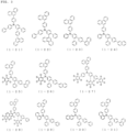
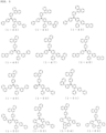
- the "substituent" in the "linear or branched alkyl of 1 to 6 carbon atoms having a substituent", the “cycloalkyl of 5 to 10 carbon atoms having a substituent", or the “linear or branched alkenyl of 2 to 6 carbon atoms having a substituent” represented by R 1 to R 3 in the general formula (1) include a deuterium atom; cyano; nitro; halogen atoms such as a fluorine atom, a chlorine atom, a bromine atom, and an iodine atom; linear or branched alkyloxy of 1 to 6 carbon atoms such as methyloxy, ethyloxy, and propyloxy; alkenyl such as vinyl, and allyl; aryloxy such as phenyloxy, and tolyloxy; arylalkyloxy such as benzyloxy, and phenethyloxy; aromatic hydrocarbon groups or condensed polycyclic aromatic
- substituents may have a substituent, and examples of the substituent include the same substituents exemplified as the "substituent" in the "linear or branched alkyl of 1 to 6 carbon atoms having a substituent", the “cycloalkyl of 5 to 10 carbon atoms having a substituent”, or the “linear or branched alkenyl of 2 to 6 carbon atoms having a substituent” represented by R 1 to R 3 in the general formula (1).
- aromatic hydrocarbon group the "aromatic heterocyclic group”, or the “condensed polycyclic aromatic group” in the "substituted or unsubstituted aromatic hydrocarbon group", the "substituted or unsubstituted aromatic heterocyclic group”, or the "substituted or unsubstituted condensed polycyclic aromatic group” represented by R 1 to R 3 in the general formula (1)
- substituents include a deuterium atom; cyano; nitro; halogen atoms such as a fluorine atom, a chlorine atom, a bromine atom, and an iodine atom; linear or branched alkyls of 1 to 6 carbon atoms such as methyl, ethyl, n-propyl, isopropyl, n-butyl, isobutyl, tert-butyl, n-pentyl, isopentyl, neopentyl, and n-hexyl; linear or branched alkyloxy of 1 to 6 carbon atoms such as methyloxy, ethyloxy, and propyloxy; alkenyl such as vinyl, and allyl; aryloxy such as phenyloxy, and tolyloxy; arylalkyloxy such as benzyloxy, and phenethyloxy;
- aryloxy group in the "substituted or unsubstituted aryloxy group” represented by R 1 to R 3 in the general formula (1) include a phenyloxy group, a biphenylyloxy group, a terphenylyloxy group, a naphthyloxy group, an anthracenyloxy group, a phenanthrenyloxy group, a fluorenyloxy group, an indenyloxy group, a pyrenyloxy group, and a perylenyloxy group.
- These groups may have a substituent, and examples of the substituent include the same substituents exemplified as the "substituent" that the "aromatic hydrocarbon group", the “aromatic heterocyclic group”, or the “condensed polycyclic aromatic group” in the "substituted or unsubstituted aromatic hydrocarbon group", the "substituted or unsubstituted aromatic heterocyclic group", or the "substituted or unsubstituted condensed polycyclic aromatic group” represented by R 1 to R 3 in the general formula (1) may have.
- the "divalent group of aromatic hydrocarbon", the "divalent group of aromatic heterocyclic ring”, or the “divalent group of condensed polycyclic aromatics” in the "divalent group of a substituted or unsubstituted aromatic hydrocarbon", the "divalent group of a substituted or unsubstituted aromatic heterocyclic ring”, or the "divalent group of substituted or unsubstituted condensed polycyclic aromatics” represented by A 1 in the general formula (1) is a divalent group that results from the removal of two hydrogen atoms from the above "aromatic hydrocarbon", “aromatic heterocyclic ring”, or "condensed polycyclic aromatics".
- These groups may have a substituent, and examples of the substituent include the same substituents exemplified as the "substituent" that the "aromatic hydrocarbon group", the “aromatic heterocyclic group”, or the “condensed polycyclic aromatic group” in the "substituted or unsubstituted aromatic hydrocarbon group", the "substituted or unsubstituted aromatic heterocyclic group", or the "substituted or unsubstituted condensed polycyclic aromatic group” represented by R 1 to R 3 in the general formula (1) may have.
- aromatic hydrocarbon group the "aromatic heterocyclic group”, or the “condensed polycyclic aromatic group” in the "substituted or unsubstituted aromatic hydrocarbon group", the "substituted or unsubstituted aromatic heterocyclic group”, or the "substituted or unsubstituted condensed polycyclic aromatic group” represented by Ar 1 to Ar 3 in the general formula (1)
- These groups may have a substituent, and examples of the substituent include the same substituents exemplified as the "substituent" that the "aromatic hydrocarbon group", the “aromatic heterocyclic group”, or the “condensed polycyclic aromatic group” in the "substituted or unsubstituted aromatic hydrocarbon group", the "substituted or unsubstituted aromatic heterocyclic group", or the "substituted or unsubstituted condensed polycyclic aromatic group” represented by R 1 to R 3 in the general formula (1) may have.
- a 1 is preferably the "divalent group of a substituted or unsubstituted aromatic hydrocarbon" or the "substituted or unsubstituted condensed polycyclic aromatic group", far preferably, a divalent group that results from the removal of two hydrogen atoms from benzene, biphenyl, or naphthalene, particularly preferably a divalent group that results from the removal of two hydrogen atoms from benzene.
- Ar 1 is preferably a "substituted or unsubstituted aromatic hydrocarbon group", a “substituted or unsubstituted condensed polycyclic aromatic group", a carbazolyl group, an indolyl group, a dibenzofuranyl group or a dibenzothienyl group, far preferably, a substituted or unsubstituted phenyl group, a substituted or unsubstituted biphenyl group, a substituted or unsubstituted terphenyl group, a substituted or unsubstituted naphthyl group, a substituted or unsubstituted phenanthryl group, a substituted or unsubstituted anthracenyl group, a substituted or unsubstituted fluorenyl group, a substituted or unsubstituted carbazolyl group, a substituted or unsubstituted
- Ar 3 is preferably a "substituted or unsubstituted aromatic hydrocarbon group", or a "substituted or unsubstituted condensed polycyclic aromatic group", far preferably, a substituted or unsubstituted phenyl group, a substituted or unsubstituted biphenyl group, a substituted or unsubstituted terphenyl group, a substituted or unsubstituted naphthyl group, a substituted or unsubstituted fluorenyl group, particularly preferably a substituted or unsubstituted phenyl group.
- the compounds of the general formula (1a) are far preferable.
- aromatic hydrocarbon the "condensed polycyclic aromatics", or the " aromatic heterocyclic ring” in the "substituted or unsubstituted aromatic hydrocarbon", the "substituted or unsubstituted condensed polycyclic aromatics", or the "substituted or unsubstituted aromatic heterocyclic ring” represented by Q 1 to Q 3 in the general formula (2) and the general formula (3)
- substituents may have a substituent, and examples of the substituent include the same substituents exemplified as the "substituent" that the "aromatic hydrocarbon group", the “aromatic heterocyclic group”, or the “condensed polycyclic aromatic group” in the "substituted or unsubstituted aromatic hydrocarbon group", the "substituted or unsubstituted aromatic heterocyclic group", or the "substituted or unsubstituted condensed polycyclic aromatic group” represented by R 1 to R 3 in the general formula (1) may have.
- substituents may bind to each other via a single bond, substituted or unsubstituted methylene, an oxygen atom, or a sulfur atom to form a ring.
- B is defined as a boron atom
- P is a phosphorus atom
- Y 1 to Y 3 in the general formula (2) and the general formula (3) may be the same or different, and represent one of selected from N-R 4 , CR 5 R 6 , O, S, Se, and SiR 7 R 8 .
- N-R 4 is a nitrogen atom having R 4 as a substituent
- CR 5 R 6 is a carbon atom having R 5 and R 6 as a substituent
- O is an oxygen atom
- S is a sulfur atom
- Se is a selenium atom
- SiR 7 R 8 is a silicon atom having R 7 and R 8 as a substituent.
- substituents may have a substituent, and examples of the substituent include the same substituents exemplified as the "substituent" in the "linear or branched alkyl of 1 to 6 carbon atoms having a substituent", the “cycloalkyl of 5 to 10 carbon atoms having a substituent”, or the “linear or branched alkenyl of 2 to 6 carbon atoms having a substituent” represented by R 1 to R 3 in the general formula (1).
- substituents may have a substituent, and examples of the substituent include the same substituents exemplified as the "substituent" in the "linear or branched alkyl of 1 to 6 carbon atoms having a substituent", the “cycloalkyl of 5 to 10 carbon atoms having a substituent”, or the “linear or branched alkenyl of 2 to 6 carbon atoms having a substituent” represented by R 1 to R 3 in the general formula (1).
- Y 1 to Y 3 in the general formula (2) and the general formula (3) are N-R 4 , CR 5 R 6 , or SiR 7 R 8
- specific examples of the "aromatic hydrocarbon group", or the "condensed polycyclic aromatic group” in the "substituted or unsubstituted aromatic hydrocarbon group", or the "substituted or unsubstituted condensed polycyclic aromatic group” represented by R 4 to R 8 in N-R 4 , CR 5 R 6 , or SiR 7 R 8 include phenyl, biphenyl, terphenyl, naphthyl, anthracenyl, phenanthryl.
- These groups may have a substituent, and examples of the substituent include the same substituents exemplified as the "substituent" that the "aromatic hydrocarbon group", the “aromatic heterocyclic group”, or the “condensed polycyclic aromatic group” in the "substituted or unsubstituted aromatic hydrocarbon group", the "substituted or unsubstituted aromatic heterocyclic group", or the "substituted or unsubstituted condensed polycyclic aromatic group” represented by R 1 to R 3 in the general formula (1) may have.
- Y 1 to Y 3 in the general formula (2) and the general formula (3) are N-R 4 , CR 5 R 6 , or SiR 7 R 8
- specific examples of the "aryloxy group" in the "substituted or unsubstituted aryloxy group” represented by R 4 to R 8 in N-R 4 , CR 5 R 6 , or SiR 7 R 8 include a phenyloxy group, a biphenylyloxy group, a terphenylyloxy group, a naphthyloxy group, an anthracenyloxy group, a phenanthrenyloxy group, a fluorenyloxy group, an indenyloxy group, a pyrenyloxy group, and a perylenyloxy group.
- These groups may have a substituent, and examples of the substituent include the same substituents exemplified as the "substituent" that the "aromatic hydrocarbon group", the “aromatic heterocyclic group”, or the “condensed polycyclic aromatic group” in the "substituted or unsubstituted aromatic hydrocarbon group", the "substituted or unsubstituted aromatic heterocyclic group", or the "substituted or unsubstituted condensed polycyclic aromatic group” represented by R 1 to R 3 in the general formula (1) may have.
- the "aromatic hydrocarbon group", the "aromatic heterocyclic group”, or the “condensed polycyclic aromatic group” in the "substituted or unsubstituted aromatic hydrocarbon group", the "substituted or unsubstituted aromatic heterocyclic group", or the "substituted or unsubstituted condensed polycyclic aromatic group” represented by Q 1 to Q 3 are preferably benzene, naphthalene, phenanthrene, pyridine, pyrimidine, indene, benzofuran, benzothiophene, and indol, far preferably, benzene and naphthalene.
- R 4 to R 8 in N-R 4 , CR 5 R 6 , or SiR 7 R 8 are preferably a "linear or branched alkyl group of 1 to 6 carbon atoms that may have a substituent", a "cycloalkyl group of 5 to 10 carbon atoms that may have a substituent", a "linear or branched alkenyl group of 2 to 6 carbon atoms that may have a substituent", a "linear or branched alkyloxy group of 1 to 6 carbon atoms that may have a substituent", a "cycloalkyloxy group of 5 to 10 carbon atoms that may have a substituent", a "substituted or unsubstituted aromatic hydrocarbon group", a "substituted or unsubstituted condensed polycyclic aromatic group", or
- Y 1 is preferably N-R 4 , O, or S, far preferably, O, or S.
- the arylamine compounds of the general formula (1) for preferred use in the organic EL device of the present invention, can be used as a constitutive material of a hole transport layer of an organic EL device.
- the arylamine compounds of the general formula (1) have (1) good hole injection characteristics, (2) large hole mobility, (3) excellent electron blocking ability, (4) stability in a thin-film state, and (5) excellent heat resistance.
- the high efficiency, low turn on voltage, and high durability of the organic EL device in the present invention can be achieved because of the use of the arylamine compound, which has greater hole mobility, superior electron blocking ability, superior amorphousness, and a more stable thin-film state than conventional hole transport materials.
- the arylamine compounds of the general formula (1) were purified by methods such as column chromatography, adsorption using, for example, a silica gel, activated carbon, or activated clay, recrystallization or crystallization using a solvent, and a sublimation purification method.
- the compounds were identified by an NMR analysis.
- a glass transition point (Tg), and a work function were measured as material property values.
- the glass transition point (Tg) can be used as an index of stability in a thin-film state, and the work function can be used as an index of hole transportability and electron blocking performance.
- the glass transition point (Tg) was measured by a high-sensitive differential scanning calorimeter (DSC3100SA produced by Bruker AXS) using powder.
- a 100 nm thin film was fabricated on an ITO substrate, and an ionization potential measuring device (PYS-202 produced by Sumitomo Heavy Industries, Ltd.) was used.
- the organic EL device of the present invention may have a structure including an anode, a hole transport layer, a light emitting layer, an electron transport layer, and a cathode successively formed on a substrate, optionally with a hole injection layer between the anode and hole transport layer, a hole blocking layer between the light emitting layer and the electron transport layer, and an electron injection layer between the electron transport layer and the cathode.
- Some of the organic layers in the multilayer structure may be omitted, or may serve more than one function.
- a single organic layer may serve as the hole injection layer and the hole transport layer, or as the electron injection layer and the electron transport layer, and so on.
- any of the layers may be configured to laminate two or more organic layers having the same function, and the hole transport layer may have a two-layer laminated structure, the light emitting layer may have a two-layer laminated structure, the electron transport layer may have a two-layer laminated structure, and so on.
- the organic EL device of the present invention is preferably configured such that the hole transport layer has a two-layer laminated structure of a first hole transport layer and a second hole transport layer.
- the second hole transport layer is preferably adjacent to a light emitting layer, and it can function as an electron blocking layer.
- Electrode materials with high work functions such as ITO and gold are used as the anode of the organic EL device of the present invention.
- the hole injection layer of the organic EL device of the present invention may be made of, for example, various triphenylamine derivatives such as starburst-type triphenylamine derivatives and various triphenylamine tetramers; porphyrin compounds as represented by copper phthalocyanine; accepting heterocyclic compounds such as hexacyano azatriphenylene; and coating-type polymer materials. These materials may be formed into a thin film by a vapor deposition method or other known methods such as a spin coating method and an inkjet method.
- the arylamine compounds of the general formula (1) are used as the hole transport layer of the organic EL device of the present invention.
- Examples of a hole transporting material that can be mixed or can be used at the same time with the arylamine compounds of the general formula (1) can be the organic amine compounds such as various triphenylamine derivatives such as arylamine compounds having a structure in which four triphenylamine structures are joined within a molecule via a single bond or a divalent group that does not contain a heteroatom; and arylamine compounds having a structure in which two triphenylamine structures are joined within a molecule via a single bond or a divalent group that does not contain a heteroatom, in addition to benzidine derivatives such as N,N'-diphenyl-N,N'-di(m-tolyl)benzidine (TPD), N,N'-diphenyl-N,N'-di( ⁇ -naphthyl)benzidine (NPD), and N,N,N'
- These may be individually deposited for film forming, may be used as a single layer deposited mixed with other materials, or may be formed as a laminate of individually deposited layers, a laminate of mixedly deposited layers, or a laminate of the individually deposited layer and the mixedly deposited layer. These materials may be formed into a thin film by a vapor deposition method or other known methods such as a spin coating method and an inkjet method.
- the material used for the hole injection layer or the hole transport layer may be obtained by p-doping materials such as trisbromophenylamine hexachloroantimony, and radialene derivatives (refer to Patent Document 6, for example) into a material commonly used for these layers, or may be, for example, polymer compounds each having, as a part of the compound structure, a structure of a benzidine derivative such as TPD.
- the hole transport layer of the organic EL device of the present invention has a two-layer structure of a first hole transport layer and a second hole transport layer
- the arylamine compounds of the general formula (1) are used as the second hole transport layer located on the light emitting layer side.
- Examples of a hole transporting material that can be mixed or can be used at the same time with the arylamine compounds of the general formula (1) can be compounds having an electron blocking effect, including, for example, carbazole derivatives such as 4,4',4"-tri(N-carbazolyl)triphenylamine (TCTA), 9,9-bis[4-(carbazol-9-yl)phenyl]fluorene, 1,3-bis(carbazol-9-yl)benzene (mCP), and 2,2-bis[4-(carbazol-9-yl)phenyl]adamantane (Ad-Cz); and compounds having a triphenylsilyl group and a triarylamine structure, as represented by 9-[4-(carbazol-9-yl)phenyl]-9-[4-(triphenylsilyl)phenyl] -9H-fluorene.
- carbazole derivatives such as 4,4',4"-tri(N-carbazolyl)triphenyl
- These may be individually deposited for film forming, may be used as a single layer deposited mixed with other materials, or may be formed as a laminate of individually deposited layers, a laminate of mixedly deposited layers, or a laminate of the individually deposited layer and the mixedly deposited layer. These materials may be formed into a thin film by using a vapor deposition method or other known methods such as a spin coating method and an inkjet method.
- Material used for the light emitting layer of the organic EL device of the present invention can be preferably the compounds represented by the general formula (2) or the general formula (3).
- various metal complexes in addition to the quinolinol derivative metal complexes such as Alq 3 ; anthracene derivatives; bis(styryl)benzene derivatives; pyrene derivatives; oxazole derivatives; and polyparaphenylene vinylene derivatives can be used.
- the light emitting layer may be made of a host material and a dopant material. In that case, as the host material, an anthracene derivative having an anthracene skeleton in the molecule is preferably used.
- a pyrene derivative having a pyrene skeleton in the molecule and a compound represented by the general formula (2), or the general formula (3) are preferably used.
- heterocyclic compound having an indole ring as a partial structure of the fused ring heterocyclic compound having a carbazole ring as a partial structure of fused ring; carbazole derivative; thiazole derivative; benzimidazole derivative; polydialkylfluorene derivative; quinacridone, coumarin, rubrene, perylene, derivatives thereof; benzopyran derivative; indenophenanthrene derivatives; rhodamine derivatives; and aminostyryl derivatives can be used.
- the light-emitting material may be a phosphorescent material.
- Phosphorescent materials as metal complexes of metals such as iridium and platinum may be used.
- the phosphorescent materials include green phosphorescent materials such as Ir(ppy) 3 , blue phosphorescent materials such as FIrpic and FIr6, and red phosphorescent materials such as Btp 2 Ir(acac).
- an anthracene derivative having an anthracene skeleton in the molecule is preferably used for the host material.
- carbazole derivatives such as 4,4'-di(N-carbazolyl)biphenyl (CBP), TCTA, and mCP may be used as the hole injecting and transporting host material.
- the doping of the host material with the phosphorescent light-emitting material should preferably be made by co-evaporation in a range of 1 to 30 weight percent with respect to the whole light emitting layer.
- These materials may be formed into a thin film by using a vapor deposition method or other known methods such as a spin coating method and an inkjet method.
- the hole blocking layer of the organic EL device of the present invention may be formed by using hole blocking compounds such as various rare earth complexes, triazole derivatives, triazine derivatives, and oxadiazole derivatives, in addition to the metal complexes of phenanthroline derivatives such as bathocuproin (BCP), and the metal complexes of quinolinol derivatives such as aluminum(III) bis(2-methyl-8-quinolinate)-4-phenylphenolate (BAlq). These materials may also serve as the material of the electron transport layer.
- hole blocking compounds such as various rare earth complexes, triazole derivatives, triazine derivatives, and oxadiazole derivatives
- phenanthroline derivatives such as bathocuproin (BCP)
- BCP bathocuproin
- quinolinol derivatives such as aluminum(III) bis(2-methyl-8-quinolinate)-4-phenylphenolate (BAlq).
- These may be individually deposited for film forming, may be used as a single layer deposited mixed with other materials, or may be formed as a laminate of individually deposited layers, a laminate of mixedly deposited layers, or a laminate of the individually deposited layer and the mixedly deposited layer. These materials may be formed into a thin film by using a vapor deposition method or other known methods such as a spin coating method and an inkjet method.
- the electron transport layer of the organic EL device of the present invention may be formed by using metal complexes of quinolinol derivatives such as Alq 3 and BAlq, various metal complexes, triazole derivatives, triazine derivatives, oxadiazole derivatives, pyridine derivatives, pyrimidine derivatives, benzimidazole derivatives, thiadiazole derivatives, anthracene derivatives, carbodiimide derivatives, quinoxaline derivatives, pyridoindole derivatives, phenanthroline derivatives, and silole derivatives.
- quinolinol derivatives such as Alq 3 and BAlq
- These may be individually deposited for film forming, may be used as a single layer deposited mixed with other materials, or may be formed as a laminate of individually deposited layers, a laminate of mixedly deposited layers, or a laminate of the individually deposited layer and the mixedly deposited layer. These materials may be formed into a thin film by using a vapor deposition method or other known methods such as a spin coating method and an inkjet method.
- Examples of material used for the electron injection layer of the organic EL device of the present invention can be alkali metal salts such as lithium fluoride and cesium fluoride; alkaline earth metal salts such as magnesium fluoride; metal complexes of quinolinol derivatives such as lithium quinolinol; metal oxides such as aluminum oxide; and metals such as itterbium (Yb), samarium (Sm), calcium (Ca), strontium (Sr), cesium (Cs).
- the electron injection layer may be omitted in the preferred selection of the electron transport layer and the cathode.
- a material obtained by further N-doping a material which is commonly used for the layer with a metal such as cesum, or the like can be used.
- the cathode of the organic EL device of the present invention may be made of an electrode material with a low work function such as aluminum, or an alloy of an electrode material with an even lower work function such as a magnesium-silver alloy, a magnesium-indium alloy, or an aluminum-magnesium alloy.
- Biphenyl-4-yl-(6-bromo-[1,1';4.',1"]terphenyl-3-yl)-(4-phenanthrene-9-yl-phenyl)-amine 10.0 g
- phenylboronic acid 2.5 g
- potassium carbonate 3.6 g
- toluene 80 mL
- ethanol 30 mL
- water 30 mL
- tetrakis(triphenylphosphine)palladium (0): 0.3 g was added thereto, and the mixture was stirred under reflux overnight.
- Biphenyl-4-yl-(6-bromo-4'-naphthalene-1-yl-biphenyl-3-yl)-(4-phenanthrene-9-yl-phenyl)-amine 10.0 g
- phenylboronic acid 2.3 g
- potassium carbonate 3.4 g
- toluene 80 mL
- ethanol 30 mL
- water 30 mL
- tetrakis(triphenylphosphine)palladium (0): 0.3 g was added thereto, and the mixture was stirred under reflux overnight.
- Biphenyl-4-yl-(6-bromo-4'-naphthalene-2-yl-biphenyl-3-yl)-(4-phenanthrene-9-yl-phenyl)-amine 10.0 g
- phenylboronic acid 2.3 g
- potassium carbonate 3.4 g
- toluene 80 mL
- ethanol 30 mL
- water 30 mL
- tetrakis(triphenylphosphine)palladium (0): 0.3 g was added thereto, and the mixture was stirred under reflux overnight.
- Biphenyl-4-yl-[1,2';1',1";4",1′′′]quarterphenyl-4'-yl-amine 14.5 g
- 9-(4-bromo-phenyl)-phenanthrene 9.3 g
- tert-butoxy sodium 3.2 g
- toluene 93 mL
- palladium(II) acetate 0.1 g
- tri(tert-butyl)phosphine 0.2 g were added thereto, and the mixture was refluxed and stirred for 3 hours.
- the structure of the obtained white powder was identified by NMR.
- the glass transition points (Tg) of the arylamine compounds of the general formula (1) were determined using a high-sensitive differential scanning calorimeter (DSC3100SA produced by Bruker AXS).
- the arylamine compounds of the general formula (1) have glass transition points (Tg) of 100 °C or higher, demonstrating that the compounds have a stable thin-film state.
- a 100 nm-thick vapor-deposited film was fabricated on an ITO substrate using the arylamine compounds of the general formula (1), and a work function was measured using an ionization potential measuring device (PYS-202 produced by Sumitomo Heavy Industries, Ltd.).
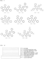
- the organic EL device as shown in FIG. 10 , was fabricated by vapor-depositing a hole injection layer 3, a first hole transport layer 4, a second hole transport layer 5, a light emitting layer 6, an electron transport layer 7, an electron injection layer 8, and a cathode (aluminum electrode) 9 in this order on a glass substrate 1 on which an ITO electrode was formed as a transparent anode 2 beforehand.
- the electron injection layer 8 was formed on the electron transport layer 7 by forming lithium fluoride in a film thickness of 1 nm.
- the cathode 9 was formed by vapor-depositing aluminum in a thickness of 100 nm.
- Table 1 summarizes the results of emission characteristics measurements performed by applying a DC voltage to the fabricated organic EL device.
- An organic EL device was fabricated under the same conditions used in Example 17, except that the second hole transport layer 5 was formed by forming the compound (1-3) of Example 2, instead of using the compound (1-2) of Example 1.
- the characteristics of the organic EL device thus fabricated were measured in the atmosphere at an ordinary temperature. Table 1 summarizes the results of emission characteristics measurements performed by applying a DC voltage to the fabricated organic EL device.
- An organic EL device was fabricated under the same conditions used in Example 17, except that the second hole transport layer 5 was formed by forming the compound (1-4) of Example 3, instead of using the compound (1-2) of Example 1.
- the characteristics of the organic EL device thus fabricated were measured in the atmosphere at an ordinary temperature. Table 1 summarizes the results of emission characteristics measurements performed by applying a DC voltage to the fabricated organic EL device.
- An organic EL device was fabricated under the same conditions used in Example 17, except that the second hole transport layer 5 was formed by forming the compound (1-6) of Example 5, instead of using the compound (1-2) of Example 1.
- the characteristics of the organic EL device thus fabricated were measured in the atmosphere at an ordinary temperature. Table 1 summarizes the results of emission characteristics measurements performed by applying a DC voltage to the fabricated organic EL device.
- An organic EL device was fabricated under the same conditions used in Example 17, except that the second hole transport layer 5 was formed by forming the compound (1-7) of Example 6, instead of using the compound (1-2) of Example 1.
- the characteristics of the organic EL device thus fabricated were measured in the atmosphere at an ordinary temperature. Table 1 summarizes the results of emission characteristics measurements performed by applying a DC voltage to the fabricated organic EL device.
- An organic EL device was fabricated under the same conditions used in Example 17, except that the second hole transport layer 5 was formed by forming the compound (1-12) of Example 7, instead of using the compound (1-2) of Example 1.
- the characteristics of the organic EL device thus fabricated were measured in the atmosphere at an ordinary temperature. Table 1 summarizes the results of emission characteristics measurements performed by applying a DC voltage to the fabricated organic EL device.
- An organic EL device was fabricated under the same conditions used in Example 17, except that the second hole transport layer 5 was formed by forming the compound (1-23) of Example 8, instead of using the compound (1-2) of Example 1.
- the characteristics of the organic EL device thus fabricated were measured in the atmosphere at an ordinary temperature. Table 1 summarizes the results of emission characteristics measurements performed by applying a DC voltage to the fabricated organic EL device.
- An organic EL device was fabricated under the same conditions used in Example 17, except that the second hole transport layer 5 was formed by forming the compound (1-24) of Example 9, instead of using the compound (1-2) of Example 1.
- the characteristics of the organic EL device thus fabricated were measured in the atmosphere at an ordinary temperature. Table 1 summarizes the results of emission characteristics measurements performed by applying a DC voltage to the fabricated organic EL device.
- An organic EL device was fabricated under the same conditions used in Example 17, except that the second hole transport layer 5 was formed by forming the compound (1-29) of Example 10, instead of using the compound (1-2) of Example 1.
- the characteristics of the organic EL device thus fabricated were measured in the atmosphere at an ordinary temperature. Table 1 summarizes the results of emission characteristics measurements performed by applying a DC voltage to the fabricated organic EL device.
- An organic EL device was fabricated under the same conditions used in Example 17, except that the second hole transport layer 5 was formed by forming the compound (1-41) of Example 11, instead of using the compound (1-2) of Example 1.
- the characteristics of the organic EL device thus fabricated were measured in the atmosphere at an ordinary temperature. Table 1 summarizes the results of emission characteristics measurements performed by applying a DC voltage to the fabricated organic EL device.
- An organic EL device was fabricated under the same conditions used in Example 17, except that the second hole transport layer 5 was formed by forming the compound (1-60) of Example 12, instead of using the compound (1-2) of Example 1.
- the characteristics of the organic EL device thus fabricated were measured in the atmosphere at an ordinary temperature. Table 1 summarizes the results of emission characteristics measurements performed by applying a DC voltage to the fabricated organic EL device.
- An organic EL device was fabricated under the same conditions used in Example 17, except that the second hole transport layer 5 was formed by forming the compound (1-61) of Example 13, instead of using the compound (1-2) of Example 1.
- the characteristics of the organic EL device thus fabricated were measured in the atmosphere at an ordinary temperature. Table 1 summarizes the results of emission characteristics measurements performed by applying a DC voltage to the fabricated organic EL device.
- an organic EL device was fabricated under the same conditions used in Example 17, except that the second hole transport layer 5 was formed by forming a compound (HTM-2) of the structural formula below, instead of using the compound (1-2) of Example 1.
- the characteristics of the organic EL device thus fabricated were measured in the atmosphere at an ordinary temperature. Table 1 summarizes the results of emission characteristics measurements performed by applying a DC voltage to the fabricated organic EL device.
- an organic EL device was fabricated under the same conditions used in Example 17, except that the second hole transport layer 5 was formed by forming a compound (HTM-3) of the structural formula below, instead of using the compound (1-2) of Example 1.
- the characteristics of the organic EL device thus fabricated were measured in the atmosphere at an ordinary temperature. Table 1 summarizes the results of emission characteristics measurements performed by applying a DC voltage to the fabricated organic EL device.
- an organic EL device was fabricated under the same conditions used in Example 17, except that the second hole transport layer 5 was formed by forming a compound (HTM-4) of the structural formula below, instead of using the compound (1-2) of Example 1.
- the characteristics of the organic EL device thus fabricated were measured in the atmosphere at an ordinary temperature. Table 1 summarizes the results of emission characteristics measurements performed by applying a DC voltage to the fabricated organic EL device.
- Table 1 summarizes the results of the device lifetime measurements performed with the organic EL devices fabricated in Examples 42 to 51 and Comparative Examples 1 to 4.
- a device lifetime was measured as the time elapsed until the emission luminance of 2,000 cd/m 2 (initial luminance) at the start of emission was attenuated to 1,900 cd/m 2 (corresponding to attenuation to 95% when taking the initial luminance as 100%) when carrying out constant current driving.
- the current efficiency upon passing a current with a current density of 10 mA/cm 2 was 10.04 to 11.18 cd/A for the organic EL devices in Examples 17 to 29, which was higher than 7.42 to 9.34 cd/A for the organic EL devices in Comparative Examples 1 to 3.
- the power efficiency was 8.65 to 9.82 lm/W for the organic EL devices in Examples 17 to 29, which was higher than 6.26 to 7.91 lm/W for the organic EL devices in Comparative Examples 1 to 3.
- Table 1 also shows that the device lifetime (attenuation to 95%) was 285 to 356 hours for the organic EL devices in Examples 17 to 29, showing achievement of a far longer lifetime than 206 to 235 hours for the organic EL devices in Comparative Examples 1 to 3.
- the organic EL device of the Example using the material of the present invention can achieve an organic EL device having high luminous efficiency and a long lifetime compared to the organic EL devices of the Comparative example using the conventional material by using the arylamine compound having a specific structure represented by the general formula (1) has greater hole mobility, and superior electron blocking ability than conventional arylamine compounds used in Comparative Examples 1 to 3.
- organic EL device of the present invention in which an arylamine compound having a specific structure are using, luminous efficiency can be improved, and also durability of the organic EL device can be improved to attain potential applications for, for example, home electric appliances and illuminations.
Landscapes
- Chemical & Material Sciences (AREA)
- Organic Chemistry (AREA)
- Engineering & Computer Science (AREA)
- Materials Engineering (AREA)
- Physics & Mathematics (AREA)
- Spectroscopy & Molecular Physics (AREA)
- Optics & Photonics (AREA)
- Inorganic Chemistry (AREA)
- Electroluminescent Light Sources (AREA)
Claims (10)
- Organische Elektrolumineszenzvorrichtung, umfassend mindestens eine Anode (2), eine Lochtransportschicht (4, 5), eine lichtemittierende Schicht (6), eine Elektronentransportschicht (7) und eine Kathode (9) in dieser Reihenfolge, wobei die Lochtransportschicht eine Arylaminverbindung der folgenden allgemeinen Formel (1) umfasst:
 wobei R1 und R2 ein Deuteriumatom, ein Fluoratom, ein Chloratom, eine Cyanogruppe, eine Nitrogruppe, eine lineare oder verzweigte Alkylgruppe mit 1 bis 6 Kohlenstoffatomen, die einen Substituenten aufweisen kann, eine Cycloalkylgruppe mit 5 bis 10 Kohlenstoffatomen, die einen Substituenten aufweisen kann, eine lineare oder verzweigte Alkenylgruppe mit 2 bis 6 Kohlenstoffatomen, die einen Substituenten aufweisen kann, eine lineare oder verzweigte Alkyloxygruppe mit 1 bis 6 Kohlenstoffatomen, die einen Substituenten aufweisen kann, eine Cycloalkyloxygruppe mit 5 bis 10 Kohlenstoffatomen, die einen Substituenten aufweisen kann, eine substituierte oder unsubstituierte aromatische Kohlenwasserstoffgruppe, eine substituierte oder unsubstituierte aromatische heterozyklische Gruppe, eine substituierte oder unsubstituierte kondensierte polyzyklische aromatische Gruppe oder eine substituierte oder unsubstituierte Aryloxygruppe darstellen;R3 ein Wasserstoffatom, ein Deuteriumatom, ein Fluoratom, ein Chloratom, eine Cyanogruppe, eine Nitrogruppe, eine lineare oder verzweigte Alkylgruppe mit 1 bis 6 Kohlenstoffatomen, die einen Substituenten aufweisen kann, eine Cycloalkylgruppe mit 5 bis 10 Kohlenstoffatomen, die einen Substituenten aufweisen kann, eine lineare oder verzweigte Alkenylgruppe mit 2 bis 6 Kohlenstoffatomen, die einen Substituenten aufweisen kann, eine lineare oder verzweigte Alkyloxygruppe mit 1 bis 6 Kohlenstoffatomen, die einen Substituenten aufweisen kann, eine Cycloalkyloxygruppe mit 5 bis 10 Kohlenstoffatomen, die einen Substituenten aufweisen kann, eine substituierte oder unsubstituierte aromatische Kohlenwasserstoffgruppe, eine substituierte oder unsubstituierte aromatische heterozyklische Gruppe, eine substituierte oder unsubstituierte kondensierte polyzyklische aromatische Gruppe oder eine substituierte oder unsubstituierte Aryloxygruppe darstellt;A1 eine divalente Gruppe eines substituierten oder unsubstituierten aromatischen Kohlenwasserstoffs, eine divalente Gruppe eines substituierten oder unsubstituierten aromatischen heterozyklischen Rings oder eine divalente Gruppe von substituierten oder unsubstituierten kondensierten polyzyklischen Aromaten darstellt;Ar1 bis Ar3 eine substituierte oder unsubstituierte aromatische Kohlenwasserstoffgruppe, eine substituierte oder unsubstituierte aromatische heterozyklische Gruppe oder eine substituierte oder unsubstituierte kondensierte polyzyklische aromatische Gruppe darstellen;r1 und r2 ganze Zahlen von 0 bis 4 darstellen.
 - Organische Elektrolumineszenzvorrichtung nach Anspruch 1, wobei die Lochtransportschicht eine Zweischichtstruktur aus einer ersten Lochtransportschicht (4) und einer zweiten Lochtransportschicht (5) aufweist, und die zweite Lochtransportschicht die Arylaminverbindung der allgemeinen Formel (1) enthält.
- Organische Elektrolumineszenzvorrichtung nach Anspruch 1 oder 2, wobei die durch die allgemeine Formel (1) dargestellte Arylaminverbindung eine durch die folgende allgemeine Formel (1a) dargestellte Arylaminverbindung ist,


- Organische Elektrolumineszenzvorrichtung nach einem der Ansprüche 1 bis 3, wobei Ar3 in der allgemeinen Formel (1) oder der allgemeinen Formel (1a) eine substituierte oder unsubstituierte Phenylgruppe darstellt.
- Organische Elektrolumineszenzvorrichtung nach einem der Ansprüche 1 bis 4, wobei A1 in der allgemeinen Formel (1) oder der allgemeinen Formel (1a) eine divalente Gruppe darstellt, die aus der Entfernung von zwei Wasserstoffatomen aus substituiertem oder unsubstituiertem Benzol resultiert.
- Organische Elektrolumineszenzvorrichtung nach einem der Ansprüche 1 bis 5, wobei die lichtemittierende Schicht einen blaues Licht emittierenden Dotierstoff enthält.
- Organische Elektrolumineszenzvorrichtung nach Anspruch 6, wobei der blaues Licht emittierende Dotierstoff ein Pyren-Derivat mit einem Pyrengerüst im Molekül ist.
- Organische Elektrolumineszenzvorrichtung nach Anspruch 6, wobei der blaues Licht emittierende Dotierstoff eine Verbindung ist, die durch die folgende allgemeine Formel (2) oder allgemeine Formel (3) dargestellt ist,


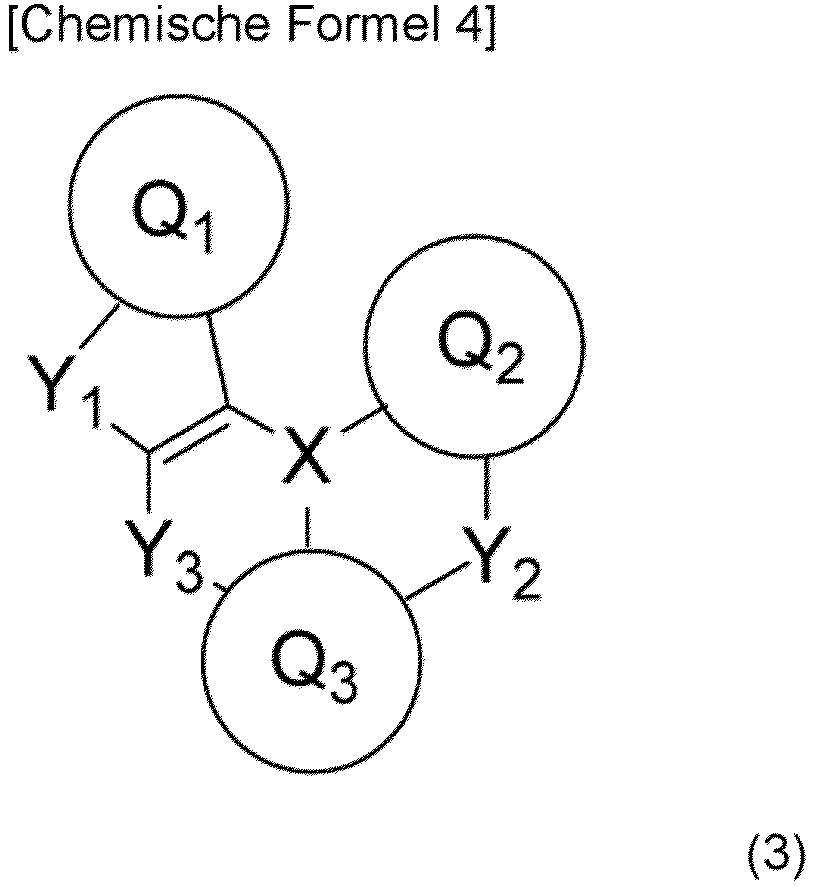 wobei Q1 bis Q3 gleich oder verschieden sein können und einen substituierten oder unsubstituierten aromatischen Kohlenwasserstoff, einen substituierten oder unsubstituierten kondensierten polyzyklischen Aromaten oder einen substituierten oder unsubstituierten aromatischen heterozyklischen Ring darstellen;X B, P, P = O oder P = S darstellt;Y1 bis Y3 gleich oder verschieden sein können und eines, ausgewählt aus N-R4, CR5R6, O, S, Se und SiR7R8, darstellen;R4 bis Ra gleich oder verschieden sein können und ein Wasserstoffatom, ein Deuteriumatom, ein Fluoratom, ein Chloratom, eine Cyanogruppe, eine Nitrogruppe, eine lineare oder verzweigte Alkylgruppe mit 1 bis 6 Kohlenstoffatomen, die einen Substituenten aufweisen kann, eine Cycloalkylgruppe mit 5 bis 10 Kohlenstoffatomen, die einen Substituenten aufweisen kann, eine lineare oder verzweigte Alkenylgruppe mit 2 bis 6 Kohlenstoffatomen, die einen Substituenten aufweisen kann, eine lineare oder verzweigte Alkyloxygruppe mit 1 bis 6 Kohlenstoffatomen, die einen Substituenten aufweisen kann, eine Cycloalkyloxygruppe mit 5 bis 10 Kohlenstoffatomen, die einen Substituenten aufweisen kann, eine substituierte oder unsubstituierte aromatische Kohlenwasserstoffgruppe, eine substituierte oder unsubstituierte kondensierte polyzyklische aromatische Gruppe oder eine substituierte oder unsubstituierte Aryloxygruppe darstellen;R5 und R6 sowie R7 und R8 über eine Einfachbindung, substituiertes oder unsubstituiertes Methylen, ein Sauerstoffatom oder ein Schwefelatom miteinander verbunden sein können, um einen Ring zu bilden;wobei, wenn Y1 bis Y3 N-R4, CR5R6 oder SiR7R8 sind, R4 bis Ra an Q1, Q2 oder Q3, die jeweils an R4 bis Ra angrenzen, binden können, um einen Ring über eine Verknüpfungsgruppe, wie substituiertes oder unsubstituiertes Methylen, ein Sauerstoffatom, ein Schwefelatom oder eine monosubstituierte Aminogruppe, zu bilden.
 - Organische Elektrolumineszenzvorrichtung nach einem der Ansprüche 1 bis 8, wobei die lichtemittierende Schicht ein Anthracenderivat mit einem Anthracengerüst im Molekül enthält.
- Organische Elektrolumineszenzvorrichtung nach Anspruch 9, wobei die lichtemittierende Schicht ein Wirtsmaterial enthält, das ein Anthracenderivat mit einem Anthracengerüst im Molekül ist.
Applications Claiming Priority (2)
| Application Number | Priority Date | Filing Date | Title |
|---|---|---|---|
| JP2019192483 | 2019-10-23 | ||
| PCT/JP2020/039313 WO2021079856A1 (ja) | 2019-10-23 | 2020-10-20 | 有機エレクトロルミネッセンス素子 |
Publications (3)
| Publication Number | Publication Date |
|---|---|
| EP4050083A1 EP4050083A1 (de) | 2022-08-31 |
| EP4050083A4 EP4050083A4 (de) | 2023-11-15 |
| EP4050083B1 true EP4050083B1 (de) | 2024-10-16 |
Family
ID=75619421
Family Applications (1)
| Application Number | Title | Priority Date | Filing Date |
|---|---|---|---|
| EP20878630.1A Active EP4050083B1 (de) | 2019-10-23 | 2020-10-20 | Organisches elektrolumineszentes element |
Country Status (7)
| Country | Link |
|---|---|
| US (1) | US20220416165A1 (de) |
| EP (1) | EP4050083B1 (de) |
| JP (1) | JP7592020B2 (de) |
| KR (1) | KR102829841B1 (de) |
| CN (1) | CN114586189B (de) |
| TW (1) | TWI872139B (de) |
| WO (1) | WO2021079856A1 (de) |
Families Citing this family (2)
| Publication number | Priority date | Publication date | Assignee | Title |
|---|---|---|---|---|
| KR20210067946A (ko) * | 2019-11-29 | 2021-06-08 | 주식회사 엘지화학 | 유기 발광 소자 |
| JPWO2025023181A1 (de) * | 2023-07-21 | 2025-01-30 |
Citations (1)
| Publication number | Priority date | Publication date | Assignee | Title |
|---|---|---|---|---|
| WO2019093649A1 (ko) * | 2017-11-10 | 2019-05-16 | 주식회사 엘지화학 | 신규한 화합물 및 이를 이용한유기 발광 소자 |
Family Cites Families (28)
| Publication number | Priority date | Publication date | Assignee | Title |
|---|---|---|---|---|
| JPS4943840B1 (de) | 1970-12-25 | 1974-11-25 | ||
| JP3194657B2 (ja) | 1993-11-01 | 2001-07-30 | 松下電器産業株式会社 | 電界発光素子 |
| JP3828595B2 (ja) | 1994-02-08 | 2006-10-04 | Tdk株式会社 | 有機el素子 |
| EP1437395B2 (de) * | 2002-12-24 | 2015-08-26 | LG Display Co., Ltd. | Organische elektrolumineszierende Vorrichtung |
| KR100787425B1 (ko) | 2004-11-29 | 2007-12-26 | 삼성에스디아이 주식회사 | 페닐카바졸계 화합물 및 이를 이용한 유기 전계 발광 소자 |
| CN1956945B (zh) | 2004-05-25 | 2010-09-22 | 保土谷化学工业株式会社 | 对三联苯化合物和使用该化合物的电子照相用感光体 |
| JP2008048656A (ja) | 2006-08-24 | 2008-03-06 | Clion Co Ltd | 水槽用ろ過材集成体 |
| JP5133259B2 (ja) | 2006-11-24 | 2013-01-30 | 出光興産株式会社 | 芳香族アミン誘導体及びそれを用いた有機エレクトロルミネッセンス素子 |
| JP5249654B2 (ja) * | 2007-11-28 | 2013-07-31 | 出光興産株式会社 | フルオランテン誘導体を用いた有機エレクトロルミネッセンス素子 |
| WO2010061824A1 (ja) * | 2008-11-25 | 2010-06-03 | 出光興産株式会社 | 芳香族アミン誘導体及び有機エレクトロルミネッセンス素子 |
| EP2684932B8 (de) | 2012-07-09 | 2016-12-21 | Hodogaya Chemical Co., Ltd. | Diarylamino matrix material dotiert mit einer mesomeren radialenverbindung |
| JP2015216135A (ja) * | 2012-08-10 | 2015-12-03 | 出光興産株式会社 | 有機エレクトロルミネッセンス素子、および電子機器 |
| KR102102350B1 (ko) * | 2012-12-26 | 2020-04-21 | 삼성디스플레이 주식회사 | 아릴아민 화합물 및 이를 포함한 유기 발광 소자 |
| US10374166B2 (en) * | 2014-02-18 | 2019-08-06 | Kwansei Gakuin Educational Foundation | Polycyclic aromatic compound |
| EP3220437B1 (de) * | 2014-11-14 | 2021-04-14 | Hodogaya Chemical Co., Ltd. | Organisches elektrolumineszentes element |
| CN107210382B (zh) * | 2015-02-03 | 2020-01-10 | 保土谷化学工业株式会社 | 有机电致发光器件 |
| JP6850261B2 (ja) * | 2015-12-17 | 2021-03-31 | 株式会社半導体エネルギー研究所 | 発光素子、発光装置、電子機器および照明装置 |
| WO2017122813A1 (ja) * | 2016-01-14 | 2017-07-20 | 保土谷化学工業株式会社 | 有機エレクトロルミネッセンス素子 |
| EP3312166B1 (de) * | 2016-10-21 | 2019-11-27 | Samsung Display Co., Ltd. | Monoaminverbindung und organische elektrolumineszenzvorrichtung damit |
| KR101868505B1 (ko) * | 2016-10-21 | 2018-06-26 | 삼성디스플레이 주식회사 | 모노아민 화합물 및 이를 포함하는 유기 전계 발광 소자 |
| CN106866498A (zh) * | 2017-02-23 | 2017-06-20 | 南京高光半导体材料有限公司 | 有机化合物、有机电致发光器件及其应用 |
| KR102134382B1 (ko) * | 2017-11-10 | 2020-07-15 | 주식회사 엘지화학 | 신규한 화합물 및 이를 이용한 유기 발광 소자 |
| KR102708484B1 (ko) * | 2017-12-11 | 2024-09-24 | 주식회사 동진쎄미켐 | 신규 화합물 및 이를 포함하는 유기 발광 소자 |
| KR102192216B1 (ko) * | 2017-12-26 | 2020-12-16 | 주식회사 엘지화학 | 아민계 화합물 및 이를 포함하는 유기 발광 소자 |
| KR102094830B1 (ko) * | 2018-11-30 | 2020-03-30 | 에스에프씨 주식회사 | 다환 방향족 유도체 화합물 및 이를 이용한 유기발광소자 |
| KR102542200B1 (ko) * | 2018-12-21 | 2023-06-09 | 주식회사 엘지화학 | 화합물 및 이를 포함하는 유기 발광 소자 |
| CN113016088B (zh) * | 2019-01-14 | 2025-01-28 | 株式会社Lg化学 | 有机发光二极管 |
| JP2020136675A (ja) * | 2019-02-14 | 2020-08-31 | 学校法人関西学院 | 有機電界発光素子 |
-
2020
- 2020-10-20 CN CN202080073485.0A patent/CN114586189B/zh active Active
- 2020-10-20 KR KR1020227012125A patent/KR102829841B1/ko active Active
- 2020-10-20 JP JP2021553438A patent/JP7592020B2/ja active Active
- 2020-10-20 WO PCT/JP2020/039313 patent/WO2021079856A1/ja not_active Ceased
- 2020-10-20 EP EP20878630.1A patent/EP4050083B1/de active Active
- 2020-10-20 US US17/770,392 patent/US20220416165A1/en active Pending
- 2020-10-21 TW TW109136360A patent/TWI872139B/zh active
Patent Citations (1)
| Publication number | Priority date | Publication date | Assignee | Title |
|---|---|---|---|---|
| WO2019093649A1 (ko) * | 2017-11-10 | 2019-05-16 | 주식회사 엘지화학 | 신규한 화합물 및 이를 이용한유기 발광 소자 |
Also Published As
| Publication number | Publication date |
|---|---|
| KR20220086562A (ko) | 2022-06-23 |
| EP4050083A1 (de) | 2022-08-31 |
| US20220416165A1 (en) | 2022-12-29 |
| JP7592020B2 (ja) | 2024-11-29 |
| CN114586189B (zh) | 2025-11-21 |
| EP4050083A4 (de) | 2023-11-15 |
| TW202124356A (zh) | 2021-07-01 |
| WO2021079856A1 (ja) | 2021-04-29 |
| CN114586189A (zh) | 2022-06-03 |
| KR102829841B1 (ko) | 2025-07-04 |
| TWI872139B (zh) | 2025-02-11 |
| JPWO2021079856A1 (de) | 2021-04-29 |
Similar Documents
| Publication | Publication Date | Title |
|---|---|---|
| EP2960958B1 (de) | Organisches elektrolumineszenzelement | |
| EP3222613B1 (de) | Verbindung mit einer indencarbazolringstruktur und einer organischen elektrolumineszenzvorrichtung | |
| EP3240057B1 (de) | Organisches elektrolumineszentes element | |
| EP3282496B1 (de) | Organisches elektrolumineszentes element | |
| EP3291323B1 (de) | Organisches elektrolumineszentes element | |
| EP3255692B1 (de) | Organisches elektrolumineszentes element | |
| EP3671885B1 (de) | Organische elektrolumineszente vorrichtung | |
| EP3223330B1 (de) | Organisches elektrolumineszentes element | |
| EP2578572A1 (de) | Verbindungen mit acridan-ringstrukturen und organischen elektrolumineszierenden elementen | |
| EP3812367B1 (de) | Verbindung mit triarylaminstruktur und elektrolumineszenzvorrichtung | |
| EP3370272A1 (de) | Organische elektrolumineszente vorrichtung | |
| EP3404735B1 (de) | Organisches elektrolumineszentes element | |
| EP3544073A1 (de) | Organisches elektrolumineszenzelement | |
| EP3343657A1 (de) | Organisches elektrolumineszentes element | |
| EP3605638B1 (de) | Organische elektrolumineszente vorrichtung | |
| EP3514845B1 (de) | Indenocarbazolverbindung und organisches elektrolumineszentes element | |
| EP4116393B1 (de) | Organisches elektrolumineszenzelement | |
| EP4050083B1 (de) | Organisches elektrolumineszentes element | |
| EP4438590A1 (de) | Arylaminverbindung, organisches elektrolumineszenzelement und elektronische vorrichtung | |
| EP4198104A1 (de) | Organisches elektrolumineszenzelement | |
| EP3163644B1 (de) | Organisches elektrolumineszentes element |
Legal Events
| Date | Code | Title | Description |
|---|---|---|---|
| STAA | Information on the status of an ep patent application or granted ep patent |
Free format text: STATUS: THE INTERNATIONAL PUBLICATION HAS BEEN MADE |
|
| PUAI | Public reference made under article 153(3) epc to a published international application that has entered the european phase |
Free format text: ORIGINAL CODE: 0009012 |
|
| STAA | Information on the status of an ep patent application or granted ep patent |
Free format text: STATUS: REQUEST FOR EXAMINATION WAS MADE |
|
| 17P | Request for examination filed |
Effective date: 20220505 |
|
| AK | Designated contracting states |
Kind code of ref document: A1 Designated state(s): AL AT BE BG CH CY CZ DE DK EE ES FI FR GB GR HR HU IE IS IT LI LT LU LV MC MK MT NL NO PL PT RO RS SE SI SK SM TR |
|
| DAV | Request for validation of the european patent (deleted) | ||
| DAX | Request for extension of the european patent (deleted) | ||
| A4 | Supplementary search report drawn up and despatched |
Effective date: 20231013 |
|
| RIC1 | Information provided on ipc code assigned before grant |
Ipc: H10K 50/15 20230101ALN20231009BHEP Ipc: H10K 85/60 20230101ALI20231009BHEP Ipc: C09K 11/06 20060101AFI20231009BHEP |
|
| GRAP | Despatch of communication of intention to grant a patent |
Free format text: ORIGINAL CODE: EPIDOSNIGR1 |
|
| STAA | Information on the status of an ep patent application or granted ep patent |
Free format text: STATUS: GRANT OF PATENT IS INTENDED |
|
| RIC1 | Information provided on ipc code assigned before grant |
Ipc: H10K 50/15 20230101ALN20240530BHEP Ipc: H10K 85/60 20230101ALI20240530BHEP Ipc: C09K 11/06 20060101AFI20240530BHEP |
|
| INTG | Intention to grant announced |
Effective date: 20240625 |
|
| P01 | Opt-out of the competence of the unified patent court (upc) registered |
Free format text: CASE NUMBER: APP_41696/2024 Effective date: 20240715 |
|
| GRAS | Grant fee paid |
Free format text: ORIGINAL CODE: EPIDOSNIGR3 |
|
| GRAA | (expected) grant |
Free format text: ORIGINAL CODE: 0009210 |
|
| STAA | Information on the status of an ep patent application or granted ep patent |
Free format text: STATUS: THE PATENT HAS BEEN GRANTED |
|
| RAP3 | Party data changed (applicant data changed or rights of an application transferred) |
Owner name: SFC CO., LTD. Owner name: HODOGAYA CHEMICAL CO., LTD. |
|
| RIN1 | Information on inventor provided before grant (corrected) |
Inventor name: KIM, JI-HWAN Inventor name: YANG, BYUNG-SUN Inventor name: JOO, SUNG-HOON Inventor name: CHA, SOON-WOOK Inventor name: HAYASHI, SHUICHI Inventor name: YAMAMOTO, TAKESHI Inventor name: KASE, KOUKI Inventor name: SURUGA, KAZUYUKI |
|
| AK | Designated contracting states |
Kind code of ref document: B1 Designated state(s): AL AT BE BG CH CY CZ DE DK EE ES FI FR GB GR HR HU IE IS IT LI LT LU LV MC MK MT NL NO PL PT RO RS SE SI SK SM TR |
|
| REG | Reference to a national code |
Ref country code: GB Ref legal event code: FG4D |
|
| REG | Reference to a national code |
Ref country code: CH Ref legal event code: EP Ref country code: DE Ref legal event code: R096 Ref document number: 602020039713 Country of ref document: DE |
|
| REG | Reference to a national code |
Ref country code: IE Ref legal event code: FG4D |
|
| REG | Reference to a national code |
Ref country code: LT Ref legal event code: MG9D |
|
| REG | Reference to a national code |
Ref country code: NL Ref legal event code: MP Effective date: 20241016 |
|
| REG | Reference to a national code |
Ref country code: AT Ref legal event code: MK05 Ref document number: 1732932 Country of ref document: AT Kind code of ref document: T Effective date: 20241016 |
|
| PG25 | Lapsed in a contracting state [announced via postgrant information from national office to epo] |
Ref country code: NL Free format text: LAPSE BECAUSE OF FAILURE TO SUBMIT A TRANSLATION OF THE DESCRIPTION OR TO PAY THE FEE WITHIN THE PRESCRIBED TIME-LIMIT Effective date: 20241016 |
|
| PG25 | Lapsed in a contracting state [announced via postgrant information from national office to epo] |
Ref country code: NL Free format text: LAPSE BECAUSE OF FAILURE TO SUBMIT A TRANSLATION OF THE DESCRIPTION OR TO PAY THE FEE WITHIN THE PRESCRIBED TIME-LIMIT Effective date: 20241016 |
|
| PG25 | Lapsed in a contracting state [announced via postgrant information from national office to epo] |
Ref country code: PT Free format text: LAPSE BECAUSE OF FAILURE TO SUBMIT A TRANSLATION OF THE DESCRIPTION OR TO PAY THE FEE WITHIN THE PRESCRIBED TIME-LIMIT Effective date: 20250217 Ref country code: IS Free format text: LAPSE BECAUSE OF FAILURE TO SUBMIT A TRANSLATION OF THE DESCRIPTION OR TO PAY THE FEE WITHIN THE PRESCRIBED TIME-LIMIT Effective date: 20250216 Ref country code: HR Free format text: LAPSE BECAUSE OF FAILURE TO SUBMIT A TRANSLATION OF THE DESCRIPTION OR TO PAY THE FEE WITHIN THE PRESCRIBED TIME-LIMIT Effective date: 20241016 |
|
| PG25 | Lapsed in a contracting state [announced via postgrant information from national office to epo] |
Ref country code: FI Free format text: LAPSE BECAUSE OF FAILURE TO SUBMIT A TRANSLATION OF THE DESCRIPTION OR TO PAY THE FEE WITHIN THE PRESCRIBED TIME-LIMIT Effective date: 20241016 |
|
| PG25 | Lapsed in a contracting state [announced via postgrant information from national office to epo] |
Ref country code: BG Free format text: LAPSE BECAUSE OF FAILURE TO SUBMIT A TRANSLATION OF THE DESCRIPTION OR TO PAY THE FEE WITHIN THE PRESCRIBED TIME-LIMIT Effective date: 20241016 |
|
| PG25 | Lapsed in a contracting state [announced via postgrant information from national office to epo] |
Ref country code: ES Free format text: LAPSE BECAUSE OF FAILURE TO SUBMIT A TRANSLATION OF THE DESCRIPTION OR TO PAY THE FEE WITHIN THE PRESCRIBED TIME-LIMIT Effective date: 20241016 |
|
| PG25 | Lapsed in a contracting state [announced via postgrant information from national office to epo] |
Ref country code: NO Free format text: LAPSE BECAUSE OF FAILURE TO SUBMIT A TRANSLATION OF THE DESCRIPTION OR TO PAY THE FEE WITHIN THE PRESCRIBED TIME-LIMIT Effective date: 20250116 |
|
| PG25 | Lapsed in a contracting state [announced via postgrant information from national office to epo] |
Ref country code: GR Free format text: LAPSE BECAUSE OF FAILURE TO SUBMIT A TRANSLATION OF THE DESCRIPTION OR TO PAY THE FEE WITHIN THE PRESCRIBED TIME-LIMIT Effective date: 20250117 Ref country code: AT Free format text: LAPSE BECAUSE OF FAILURE TO SUBMIT A TRANSLATION OF THE DESCRIPTION OR TO PAY THE FEE WITHIN THE PRESCRIBED TIME-LIMIT Effective date: 20241016 Ref country code: LV Free format text: LAPSE BECAUSE OF FAILURE TO SUBMIT A TRANSLATION OF THE DESCRIPTION OR TO PAY THE FEE WITHIN THE PRESCRIBED TIME-LIMIT Effective date: 20241016 |
|
| PG25 | Lapsed in a contracting state [announced via postgrant information from national office to epo] |
Ref country code: PL Free format text: LAPSE BECAUSE OF FAILURE TO SUBMIT A TRANSLATION OF THE DESCRIPTION OR TO PAY THE FEE WITHIN THE PRESCRIBED TIME-LIMIT Effective date: 20241016 |
|
| PG25 | Lapsed in a contracting state [announced via postgrant information from national office to epo] |
Ref country code: RS Free format text: LAPSE BECAUSE OF FAILURE TO SUBMIT A TRANSLATION OF THE DESCRIPTION OR TO PAY THE FEE WITHIN THE PRESCRIBED TIME-LIMIT Effective date: 20250116 |
|
| REG | Reference to a national code |
Ref country code: CH Ref legal event code: PL |
|
| PG25 | Lapsed in a contracting state [announced via postgrant information from national office to epo] |
Ref country code: SM Free format text: LAPSE BECAUSE OF FAILURE TO SUBMIT A TRANSLATION OF THE DESCRIPTION OR TO PAY THE FEE WITHIN THE PRESCRIBED TIME-LIMIT Effective date: 20241016 |
|
| PG25 | Lapsed in a contracting state [announced via postgrant information from national office to epo] |
Ref country code: MC Free format text: LAPSE BECAUSE OF FAILURE TO SUBMIT A TRANSLATION OF THE DESCRIPTION OR TO PAY THE FEE WITHIN THE PRESCRIBED TIME-LIMIT Effective date: 20241016 |
|
| PG25 | Lapsed in a contracting state [announced via postgrant information from national office to epo] |
Ref country code: DK Free format text: LAPSE BECAUSE OF FAILURE TO SUBMIT A TRANSLATION OF THE DESCRIPTION OR TO PAY THE FEE WITHIN THE PRESCRIBED TIME-LIMIT Effective date: 20241016 |
|
| PG25 | Lapsed in a contracting state [announced via postgrant information from national office to epo] |
Ref country code: LU Free format text: LAPSE BECAUSE OF NON-PAYMENT OF DUE FEES Effective date: 20241020 Ref country code: BE Free format text: LAPSE BECAUSE OF NON-PAYMENT OF DUE FEES Effective date: 20241031 |
|
| REG | Reference to a national code |
Ref country code: DE Ref legal event code: R097 Ref document number: 602020039713 Country of ref document: DE |
|
| PG25 | Lapsed in a contracting state [announced via postgrant information from national office to epo] |
Ref country code: EE Free format text: LAPSE BECAUSE OF FAILURE TO SUBMIT A TRANSLATION OF THE DESCRIPTION OR TO PAY THE FEE WITHIN THE PRESCRIBED TIME-LIMIT Effective date: 20241016 |
|
| PG25 | Lapsed in a contracting state [announced via postgrant information from national office to epo] |
Ref country code: CH Free format text: LAPSE BECAUSE OF NON-PAYMENT OF DUE FEES Effective date: 20241031 |
|
| PG25 | Lapsed in a contracting state [announced via postgrant information from national office to epo] |
Ref country code: RO Free format text: LAPSE BECAUSE OF FAILURE TO SUBMIT A TRANSLATION OF THE DESCRIPTION OR TO PAY THE FEE WITHIN THE PRESCRIBED TIME-LIMIT Effective date: 20241016 |
|
| PG25 | Lapsed in a contracting state [announced via postgrant information from national office to epo] |
Ref country code: SK Free format text: LAPSE BECAUSE OF FAILURE TO SUBMIT A TRANSLATION OF THE DESCRIPTION OR TO PAY THE FEE WITHIN THE PRESCRIBED TIME-LIMIT Effective date: 20241016 |
|
| PG25 | Lapsed in a contracting state [announced via postgrant information from national office to epo] |
Ref country code: CZ Free format text: LAPSE BECAUSE OF FAILURE TO SUBMIT A TRANSLATION OF THE DESCRIPTION OR TO PAY THE FEE WITHIN THE PRESCRIBED TIME-LIMIT Effective date: 20241016 |
|
| PG25 | Lapsed in a contracting state [announced via postgrant information from national office to epo] |
Ref country code: IT Free format text: LAPSE BECAUSE OF FAILURE TO SUBMIT A TRANSLATION OF THE DESCRIPTION OR TO PAY THE FEE WITHIN THE PRESCRIBED TIME-LIMIT Effective date: 20241016 |
|
| REG | Reference to a national code |
Ref country code: BE Ref legal event code: MM Effective date: 20241031 |
|
| PLBE | No opposition filed within time limit |
Free format text: ORIGINAL CODE: 0009261 |
|
| STAA | Information on the status of an ep patent application or granted ep patent |
Free format text: STATUS: NO OPPOSITION FILED WITHIN TIME LIMIT |
|
| PG25 | Lapsed in a contracting state [announced via postgrant information from national office to epo] |
Ref country code: SE Free format text: LAPSE BECAUSE OF FAILURE TO SUBMIT A TRANSLATION OF THE DESCRIPTION OR TO PAY THE FEE WITHIN THE PRESCRIBED TIME-LIMIT Effective date: 20241016 |
|
| 26N | No opposition filed |
Effective date: 20250717 |
|
| GBPC | Gb: european patent ceased through non-payment of renewal fee |
Effective date: 20250116 |
|
| PG25 | Lapsed in a contracting state [announced via postgrant information from national office to epo] |
Ref country code: GB Free format text: LAPSE BECAUSE OF NON-PAYMENT OF DUE FEES Effective date: 20250116 |
|
| PG25 | Lapsed in a contracting state [announced via postgrant information from national office to epo] |
Ref country code: FR Free format text: LAPSE BECAUSE OF NON-PAYMENT OF DUE FEES Effective date: 20241216 |
|
| PG25 | Lapsed in a contracting state [announced via postgrant information from national office to epo] |
Ref country code: IE Free format text: LAPSE BECAUSE OF NON-PAYMENT OF DUE FEES Effective date: 20241020 |
|
| PGFP | Annual fee paid to national office [announced via postgrant information from national office to epo] |
Ref country code: DE Payment date: 20251029 Year of fee payment: 6 |
|
| PG25 | Lapsed in a contracting state [announced via postgrant information from national office to epo] |
Ref country code: CY Free format text: LAPSE BECAUSE OF FAILURE TO SUBMIT A TRANSLATION OF THE DESCRIPTION OR TO PAY THE FEE WITHIN THE PRESCRIBED TIME-LIMIT; INVALID AB INITIO Effective date: 20201020 |
|
| PG25 | Lapsed in a contracting state [announced via postgrant information from national office to epo] |
Ref country code: HU Free format text: LAPSE BECAUSE OF FAILURE TO SUBMIT A TRANSLATION OF THE DESCRIPTION OR TO PAY THE FEE WITHIN THE PRESCRIBED TIME-LIMIT; INVALID AB INITIO Effective date: 20201020 |