EP3514939B1 - Convertisseur triphasé et son procédé de commande - Google Patents
Convertisseur triphasé et son procédé de commande Download PDFInfo
- Publication number
- EP3514939B1 EP3514939B1 EP16917353.1A EP16917353A EP3514939B1 EP 3514939 B1 EP3514939 B1 EP 3514939B1 EP 16917353 A EP16917353 A EP 16917353A EP 3514939 B1 EP3514939 B1 EP 3514939B1
- Authority
- EP
- European Patent Office
- Prior art keywords
- phase
- regulation
- regulator
- mod
- current
- Prior art date
- Legal status (The legal status is an assumption and is not a legal conclusion. Google has not performed a legal analysis and makes no representation as to the accuracy of the status listed.)
- Active
Links
Images



Classifications
-
- H—ELECTRICITY
- H02—GENERATION; CONVERSION OR DISTRIBUTION OF ELECTRIC POWER
- H02M—APPARATUS FOR CONVERSION BETWEEN AC AND AC, BETWEEN AC AND DC, OR BETWEEN DC AND DC, AND FOR USE WITH MAINS OR SIMILAR POWER SUPPLY SYSTEMS; CONVERSION OF DC OR AC INPUT POWER INTO SURGE OUTPUT POWER; CONTROL OR REGULATION THEREOF
- H02M7/00—Conversion of AC power input into DC power output; Conversion of DC power input into AC power output
- H02M7/42—Conversion of DC power input into AC power output without possibility of reversal
- H02M7/44—Conversion of DC power input into AC power output without possibility of reversal by static converters
- H02M7/48—Conversion of DC power input into AC power output without possibility of reversal by static converters using discharge tubes with control electrode or semiconductor devices with control electrode
- H02M7/53—Conversion of DC power input into AC power output without possibility of reversal by static converters using discharge tubes with control electrode or semiconductor devices with control electrode using devices of a triode or transistor type requiring continuous application of a control signal
- H02M7/537—Conversion of DC power input into AC power output without possibility of reversal by static converters using discharge tubes with control electrode or semiconductor devices with control electrode using devices of a triode or transistor type requiring continuous application of a control signal using semiconductor devices only, e.g. single switched pulse inverters
- H02M7/5387—Conversion of DC power input into AC power output without possibility of reversal by static converters using discharge tubes with control electrode or semiconductor devices with control electrode using devices of a triode or transistor type requiring continuous application of a control signal using semiconductor devices only, e.g. single switched pulse inverters in a bridge configuration
- H02M7/53871—Conversion of DC power input into AC power output without possibility of reversal by static converters using discharge tubes with control electrode or semiconductor devices with control electrode using devices of a triode or transistor type requiring continuous application of a control signal using semiconductor devices only, e.g. single switched pulse inverters in a bridge configuration with automatic control of output voltage or current
- H02M7/53873—Conversion of DC power input into AC power output without possibility of reversal by static converters using discharge tubes with control electrode or semiconductor devices with control electrode using devices of a triode or transistor type requiring continuous application of a control signal using semiconductor devices only, e.g. single switched pulse inverters in a bridge configuration with automatic control of output voltage or current with digital control
-
- H—ELECTRICITY
- H02—GENERATION; CONVERSION OR DISTRIBUTION OF ELECTRIC POWER
- H02J—ELECTRIC POWER NETWORKS; CIRCUIT ARRANGEMENTS OR SYSTEMS FOR SUPPLYING OR DISTRIBUTING ELECTRIC POWER; SYSTEMS FOR STORING ELECTRIC ENERGY
- H02J3/00—Circuit arrangements for AC mains or AC distribution networks
- H02J3/38—Arrangements for feeding a single network from two or more generators or sources in parallel; Arrangements for feeding already energised networks from additional generators or sources in parallel
-
- H—ELECTRICITY
- H02—GENERATION; CONVERSION OR DISTRIBUTION OF ELECTRIC POWER
- H02M—APPARATUS FOR CONVERSION BETWEEN AC AND AC, BETWEEN AC AND DC, OR BETWEEN DC AND DC, AND FOR USE WITH MAINS OR SIMILAR POWER SUPPLY SYSTEMS; CONVERSION OF DC OR AC INPUT POWER INTO SURGE OUTPUT POWER; CONTROL OR REGULATION THEREOF
- H02M1/00—Details of apparatus for conversion
- H02M1/12—Arrangements for reducing harmonics from AC input or output
- H02M1/126—Arrangements for reducing harmonics from AC input or output using passive filters
-
- H—ELECTRICITY
- H02—GENERATION; CONVERSION OR DISTRIBUTION OF ELECTRIC POWER
- H02M—APPARATUS FOR CONVERSION BETWEEN AC AND AC, BETWEEN AC AND DC, OR BETWEEN DC AND DC, AND FOR USE WITH MAINS OR SIMILAR POWER SUPPLY SYSTEMS; CONVERSION OF DC OR AC INPUT POWER INTO SURGE OUTPUT POWER; CONTROL OR REGULATION THEREOF
- H02M7/00—Conversion of AC power input into DC power output; Conversion of DC power input into AC power output
- H02M7/42—Conversion of DC power input into AC power output without possibility of reversal
- H02M7/44—Conversion of DC power input into AC power output without possibility of reversal by static converters
- H02M7/48—Conversion of DC power input into AC power output without possibility of reversal by static converters using discharge tubes with control electrode or semiconductor devices with control electrode
- H02M7/483—Converters with outputs that each can have more than two voltages levels
- H02M7/487—Neutral point clamped inverters
-
- H—ELECTRICITY
- H02—GENERATION; CONVERSION OR DISTRIBUTION OF ELECTRIC POWER
- H02M—APPARATUS FOR CONVERSION BETWEEN AC AND AC, BETWEEN AC AND DC, OR BETWEEN DC AND DC, AND FOR USE WITH MAINS OR SIMILAR POWER SUPPLY SYSTEMS; CONVERSION OF DC OR AC INPUT POWER INTO SURGE OUTPUT POWER; CONTROL OR REGULATION THEREOF
- H02M7/00—Conversion of AC power input into DC power output; Conversion of DC power input into AC power output
- H02M7/42—Conversion of DC power input into AC power output without possibility of reversal
- H02M7/44—Conversion of DC power input into AC power output without possibility of reversal by static converters
- H02M7/48—Conversion of DC power input into AC power output without possibility of reversal by static converters using discharge tubes with control electrode or semiconductor devices with control electrode
- H02M7/53—Conversion of DC power input into AC power output without possibility of reversal by static converters using discharge tubes with control electrode or semiconductor devices with control electrode using devices of a triode or transistor type requiring continuous application of a control signal
- H02M7/537—Conversion of DC power input into AC power output without possibility of reversal by static converters using discharge tubes with control electrode or semiconductor devices with control electrode using devices of a triode or transistor type requiring continuous application of a control signal using semiconductor devices only, e.g. single switched pulse inverters
- H02M7/5387—Conversion of DC power input into AC power output without possibility of reversal by static converters using discharge tubes with control electrode or semiconductor devices with control electrode using devices of a triode or transistor type requiring continuous application of a control signal using semiconductor devices only, e.g. single switched pulse inverters in a bridge configuration
- H02M7/53871—Conversion of DC power input into AC power output without possibility of reversal by static converters using discharge tubes with control electrode or semiconductor devices with control electrode using devices of a triode or transistor type requiring continuous application of a control signal using semiconductor devices only, e.g. single switched pulse inverters in a bridge configuration with automatic control of output voltage or current
-
- H—ELECTRICITY
- H02—GENERATION; CONVERSION OR DISTRIBUTION OF ELECTRIC POWER
- H02M—APPARATUS FOR CONVERSION BETWEEN AC AND AC, BETWEEN AC AND DC, OR BETWEEN DC AND DC, AND FOR USE WITH MAINS OR SIMILAR POWER SUPPLY SYSTEMS; CONVERSION OF DC OR AC INPUT POWER INTO SURGE OUTPUT POWER; CONTROL OR REGULATION THEREOF
- H02M7/00—Conversion of AC power input into DC power output; Conversion of DC power input into AC power output
- H02M7/42—Conversion of DC power input into AC power output without possibility of reversal
- H02M7/44—Conversion of DC power input into AC power output without possibility of reversal by static converters
- H02M7/48—Conversion of DC power input into AC power output without possibility of reversal by static converters using discharge tubes with control electrode or semiconductor devices with control electrode
- H02M7/53—Conversion of DC power input into AC power output without possibility of reversal by static converters using discharge tubes with control electrode or semiconductor devices with control electrode using devices of a triode or transistor type requiring continuous application of a control signal
- H02M7/537—Conversion of DC power input into AC power output without possibility of reversal by static converters using discharge tubes with control electrode or semiconductor devices with control electrode using devices of a triode or transistor type requiring continuous application of a control signal using semiconductor devices only, e.g. single switched pulse inverters
- H02M7/539—Conversion of DC power input into AC power output without possibility of reversal by static converters using discharge tubes with control electrode or semiconductor devices with control electrode using devices of a triode or transistor type requiring continuous application of a control signal using semiconductor devices only, e.g. single switched pulse inverters with automatic control of output wave form or frequency
- H02M7/5395—Conversion of DC power input into AC power output without possibility of reversal by static converters using discharge tubes with control electrode or semiconductor devices with control electrode using devices of a triode or transistor type requiring continuous application of a control signal using semiconductor devices only, e.g. single switched pulse inverters with automatic control of output wave form or frequency by pulse-width modulation
-
- H—ELECTRICITY
- H02—GENERATION; CONVERSION OR DISTRIBUTION OF ELECTRIC POWER
- H02P—CONTROL OR REGULATION OF ELECTRIC MOTORS, ELECTRIC GENERATORS OR DYNAMO-ELECTRIC CONVERTERS; CONTROLLING TRANSFORMERS, REACTORS OR CHOKE COILS
- H02P27/00—Arrangements or methods for the control of AC motors characterised by the kind of supply voltage
- H02P27/04—Arrangements or methods for the control of AC motors characterised by the kind of supply voltage using variable-frequency supply voltage, e.g. inverter or converter supply voltage
- H02P27/06—Arrangements or methods for the control of AC motors characterised by the kind of supply voltage using variable-frequency supply voltage, e.g. inverter or converter supply voltage using DC to AC converters or inverters
- H02P27/08—Arrangements or methods for the control of AC motors characterised by the kind of supply voltage using variable-frequency supply voltage, e.g. inverter or converter supply voltage using DC to AC converters or inverters with pulse width modulation
-
- H—ELECTRICITY
- H02—GENERATION; CONVERSION OR DISTRIBUTION OF ELECTRIC POWER
- H02S—GENERATION OF ELECTRIC POWER BY CONVERSION OF INFRARED RADIATION, VISIBLE LIGHT OR ULTRAVIOLET LIGHT, e.g. USING PHOTOVOLTAIC [PV] MODULES
- H02S40/00—Components or accessories in combination with PV modules, not provided for in groups H02S10/00 - H02S30/00
- H02S40/30—Electrical components
- H02S40/32—Electrical components comprising DC/AC inverter means associated with the PV module itself, e.g. AC modules
-
- H—ELECTRICITY
- H03—ELECTRONIC CIRCUITRY
- H03H—IMPEDANCE NETWORKS, e.g. RESONANT CIRCUITS; RESONATORS
- H03H7/00—Multiple-port networks comprising only passive electrical elements as network components
- H03H7/01—Frequency selective two-port networks
- H03H7/0115—Frequency selective two-port networks comprising only inductors and capacitors
-
- H—ELECTRICITY
- H02—GENERATION; CONVERSION OR DISTRIBUTION OF ELECTRIC POWER
- H02M—APPARATUS FOR CONVERSION BETWEEN AC AND AC, BETWEEN AC AND DC, OR BETWEEN DC AND DC, AND FOR USE WITH MAINS OR SIMILAR POWER SUPPLY SYSTEMS; CONVERSION OF DC OR AC INPUT POWER INTO SURGE OUTPUT POWER; CONTROL OR REGULATION THEREOF
- H02M1/00—Details of apparatus for conversion
- H02M1/0003—Details of control, feedback or regulation circuits
- H02M1/0009—Devices or circuits for detecting current in a converter
-
- H—ELECTRICITY
- H02—GENERATION; CONVERSION OR DISTRIBUTION OF ELECTRIC POWER
- H02M—APPARATUS FOR CONVERSION BETWEEN AC AND AC, BETWEEN AC AND DC, OR BETWEEN DC AND DC, AND FOR USE WITH MAINS OR SIMILAR POWER SUPPLY SYSTEMS; CONVERSION OF DC OR AC INPUT POWER INTO SURGE OUTPUT POWER; CONTROL OR REGULATION THEREOF
- H02M1/00—Details of apparatus for conversion
- H02M1/0003—Details of control, feedback or regulation circuits
- H02M1/0012—Control circuits using digital or numerical techniques
-
- H—ELECTRICITY
- H02—GENERATION; CONVERSION OR DISTRIBUTION OF ELECTRIC POWER
- H02M—APPARATUS FOR CONVERSION BETWEEN AC AND AC, BETWEEN AC AND DC, OR BETWEEN DC AND DC, AND FOR USE WITH MAINS OR SIMILAR POWER SUPPLY SYSTEMS; CONVERSION OF DC OR AC INPUT POWER INTO SURGE OUTPUT POWER; CONTROL OR REGULATION THEREOF
- H02M1/00—Details of apparatus for conversion
- H02M1/12—Arrangements for reducing harmonics from AC input or output
- H02M1/123—Suppression of common mode voltage or current
-
- Y—GENERAL TAGGING OF NEW TECHNOLOGICAL DEVELOPMENTS; GENERAL TAGGING OF CROSS-SECTIONAL TECHNOLOGIES SPANNING OVER SEVERAL SECTIONS OF THE IPC; TECHNICAL SUBJECTS COVERED BY FORMER USPC CROSS-REFERENCE ART COLLECTIONS [XRACs] AND DIGESTS
- Y02—TECHNOLOGIES OR APPLICATIONS FOR MITIGATION OR ADAPTATION AGAINST CLIMATE CHANGE
- Y02E—REDUCTION OF GREENHOUSE GAS [GHG] EMISSIONS, RELATED TO ENERGY GENERATION, TRANSMISSION OR DISTRIBUTION
- Y02E10/00—Energy generation through renewable energy sources
- Y02E10/50—Photovoltaic [PV] energy
- Y02E10/56—Power conversion systems, e.g. maximum power point trackers
-
- Y—GENERAL TAGGING OF NEW TECHNOLOGICAL DEVELOPMENTS; GENERAL TAGGING OF CROSS-SECTIONAL TECHNOLOGIES SPANNING OVER SEVERAL SECTIONS OF THE IPC; TECHNICAL SUBJECTS COVERED BY FORMER USPC CROSS-REFERENCE ART COLLECTIONS [XRACs] AND DIGESTS
- Y02—TECHNOLOGIES OR APPLICATIONS FOR MITIGATION OR ADAPTATION AGAINST CLIMATE CHANGE
- Y02E—REDUCTION OF GREENHOUSE GAS [GHG] EMISSIONS, RELATED TO ENERGY GENERATION, TRANSMISSION OR DISTRIBUTION
- Y02E60/00—Enabling technologies; Technologies with a potential or indirect contribution to GHG emissions mitigation
- Y02E60/60—Arrangements for transfer of electric power between AC networks or generators via a high voltage DC link [HVCD]
Definitions
- the present invention relates to the energy and power supply field, and in particular, to a three-phase converter and a three-phase converter control method.
- a converter becomes one of key factors in application of clean energy.
- the converter is an essential unit for implementing transfer of renewable energy, such as solar photovoltaic energy, to a power grid.
- three-phase converters are one type of most widely applied converters, and are used to connect a three-phase alternating current electrical power system and a direct current electrical power system and implement energy transfer between the two systems. Energy transfer is further distinguished into two working statuses, rectification and inversion, according to different energy flow directions. Energy transfer from the direct current system to the alternating current system is referred to as inversion, and energy transfer from the alternating current system to the direct current system is referred to as rectification.
- FIG. 1 A typical system structure of the system is shown in FIG. 1 .
- a three-phase converter is connected between a direct current system and an alternating current system, and includes a switching network, a filter, and a controller that controls the switching network.
- Conversion efficiency and electric energy quality are two key technical indicators of a three-phase converter.
- a modulation method directly affects a connectivity status of switching devices, and therefore, is one of key factors that affect the conversion efficiency and electric energy quality of the three-phase converter.
- a commonly used modulation method is pulse-width modulation (PWM), that is, a width of a driving pulse of each device on a switching network is controlled.
- PWM pulse-width modulation
- a most direct implementation is to compare a carrier and a modulated wave, and control a connectivity status of a switching device by using a result of the comparison.
- PWM may be further categorized into continuous pulse-width modulation (CPWM) and discontinuous pulse-width modulation (DPWM).
- CPWM continuous pulse-width modulation
- DPWM discontinuous pulse-width modulation
- Common methods include sinusoidal pulse-width modulation (SPWM), space vector pulse-width modulation (SVPWM), and third-harmonic-injection pulse-width modulation (THIPWM).
- SPWM sinusoidal pulse-width modulation
- SVPWM space vector pulse-width modulation
- THIPWM third-harmonic-injection pulse-width modulation
- the DPWM means that a phase bridge arm of a converter is clamped on a positive direct current bus or a negative direct current bus in a specific switching period, and a switching device of this phase is always connected or always disconnected in a clamping interval and there is no switching action.
- Common DPWM modulation methods include DPWM0, DPWM1, DPWM2, DPWM3, DPWMMAX, DP
- the DPWM Compared with the CPWM, the DPWM has a smaller quantity of switching times. Therefore, a switching loss is relatively small, and a consequential benefit is that efficiency of a converter can be improved.
- a DPWM modulated wave may be implemented by superposing an equivalent common-mode component on a CPWM modulated wave.
- a DPWM modulated waveform and an SPWM modulated waveform in an industrial frequency period (50 Hz) are compared, as shown in FIG. 2 .
- a difference between the two modulated waves is a common-mode signal waveform shown in FIG. 2 .
- the DPWM modulated wave may be equivalent to a sum of SPWM wave and a common-mode signal. Therefore, an output characteristic of DPWM wave is affected by both an output characteristic of SPWM and an output characteristic of the common-mode signal, and an extra common-mode voltage source is formed at a bridge arm port of a converter.
- the common-mode voltage source and a common-mode loop in a system interact with each other, affecting system performance.
- a middle point of capacitors of the LCL filter is connected to a middle point of capacitors on a direct current bus, to form a new common-mode loop.
- This is equivalent to splitting a common-mode current generated by the converter, so that most of the common-mode current is directed back to a direct current side of the converter by using a connection loop of the LCL filter.
- a series connection of an inductor and a capacitor exists in the connection loop, and there is a natural series resonant frequency. If the frequency overlaps a frequency range of a common-mode voltage source generated because of DPWM modulation, series resonance is generated, causing sharp fluctuation of the common-mode current, thereby affecting system stability.
- TENG LIU ET AL "Virtual impedance-based active damping for LOL resonance in grid-connected voltage source inverters with grid current feedback", 2016 IEEE ENERGY CONVERSION CONGRESS AND EXPOSITION (ECCE), 1 September 2016, pages 1-8 , discloses a straightforward design method to determine the parameters of the active damping controller.
- PICAS R ET AL "Improving capacitor voltage ripples and power losses of modular multilevel converters through discontinuous modulation"
- IECON 2013 - 39TH ANNUAL CONFERENCE OF THE IEEE INDUSTRIAL ELECTRONICS SOCIETY, IEEE, 10 November 2013, pages 6233-6238 discloses a discontinuous modulation technique for reducing the amplitude of the capacitor voltage ripples and the switching losses, especially at low modulation indices.
- US 2012/249043 A1 discloses a method for pulse width modulation control of a multiple phase drive that includes identifying a set of at least one phase from the plurality of phases for the drive as eligible for clamping to one of a plurality of extreme power supply voltages, including excluding from the set of eligible phases those phases with intermediate control signal levels and excluding phases according to a proximity criterion on the control signal levels.
- a phase is selected from the set of eligible phases.
- a first offset signal is determined as a difference between a control signal level for the selected phase and an extreme control signal level associated with one of the plurality of extreme power supply voltages.
- a modified control signal is determined for each of the phases for the drive, by forming a combination of the first offset signal and a control signal level for each phase to determine the modified control signal for each phase.
- QIANG SONG ET AL "A neutral-point potential balancing algorithm for three-level NPC inverters using analytically injected zero- sequence voltage
- ANNUAL IEEE APPLIED POWER ELECTRONICS CONFERENCE AND EXPOSITION. MIAMI BEACH, FL, FEB. 9 - 13, 2003; [ANNUAL APPLIED POWER ELECTRONICS CONFERENCE], NEW YORK, NY: IEEE, US, 9 February 2003 (2003-02-09), pages 228-233 vol.1 discloses that, based on the zero-sequence component of the reference voltages, the neutral-point variation and balancing control for three-level neutral-point-clamped inverter are analyzed.
- An analytical method is proposed to accurately calculate the injected zero-sequence voltage for NP balancing. Based on the analytical analysis, the limitation of NP balancing control is revealed and the NP-fully-controllable region is presented. A real-time NP balancing algorithm is proposed as well. The feasibility of the proposed method is verified using simulation results for a 6kV/1800kVA medium voltage drive.
- Embodiments of the present invention provide a three-phase converter and a three-phase converter control method, which are used to reduce a common-mode current in the three-phase converter, thereby effectively improving stability and efficiency of the converter.
- the invention is defined by the independent claims. All the technical features of the independent claims are mandatory and not optional, irrespective of any statements to the contrary in the following passages. Preferred embodiments are described by the dependent claims.
- a three-phase converter is provided, and is configured to be connected between a direct current system and an alternating current system to perform interconversion between a direct current and an alternating current
- the three-phase converter includes a switching network, a three-phase filter connected to the switching network, a sampling unit connected to the three-phase filter, a control unit connected to the three-phase sampling unit, an active damping unit connected to both the control unit and the sampling unit, and a modulation unit connected between the active damping unit and the switching network
- the sampling unit is configured to: obtain three-phase currents i a , i b , and i c that are output by the three-phase filter, and send the three-phase currents i a , i b , and i c to the active damping unit
- the active damping unit is configured to: obtain, according to the three-phase currents i a , i b , and i c , regulation components v' a , v
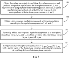
- a second aspect provides a three-phase converter control method, used to control a three-phase converter connected between a direct current system and an alternating current system to perform interconversion between a direct current and an alternating current, where the method includes: step 101: obtaining three-phase currents i a , i b , and i c in the three-phase converter, and respectively inputting the three-phase currents i a , i b , and i c one by one to corresponding current regulators G a , G b , and G c , to obtain regulation components v' a , v ' b , and v' c ; step 102: obtaining a zero-sequence regulation component v 0 through calculation according to the regulation components v' a , v ' b , and v' c ; step 103: separately adding the zero-sequence regulation component v 0 to three-phase modulated waves v a , v
- a three-phase converter in an embodiment of the present invention is configured to convert a direct current into an alternating current, or convert an alternating current into a direct current.
- a direct current generated by a photovoltaic solar panel is converted, by using a converter, into an alternating current having a same frequency as a power grid, and regulation components v' a , v ' b , and v' c ;
- step 103 separately adding the zero-sequence regulation component v 0 to three-phase modulated waves v a , v b , and v c , to obtain new three-phase modulated waves v a_mod , v b_mod , and v c_mod ;
- step 104 comparing the new three-phase modulated waves v a_mod , v b_mod , and v c_mod with a carrier signal of the three-phase converter, and outputting drive signals of switching devices of
- the obtaining a zero-sequence regulation component v 0 through calculation according to the regulation components v ' a , v ' b , and v ' c includes: calculating an average or a weighted average of the regulation components v' a , v ' b , and v ' c , where a result of the average or the weighted average is equal to the zero-sequence regulation component v 0 .
- a third aspect provides a photovoltaic system, including a photovoltaic cell panel and a three-phase converter that is connected between the photovoltaic cell panel and an alternating current power grid, where the three-phase converter is configured to obtain regulation components v' a , v ' b , and v ' c according to three-phase currents i a , i b , and i c in the three-phase converter; and the three-phase converter obtains a zero-sequence regulation component v 0 through calculation according to the regulation components v' a , v ' b , and v ' c , separately adds the zero-sequence regulation component v 0 to three-phase modulated waves v a , v b , and v c to obtain new three-phase modulated waves v a_mod , v b_mod , and v c_mod , and finally compares the new three-phase modulated waves v
- a fourth aspect provides a power system of an electric vehicle, including a direct current power source, a motor, and a three-phase converter connected between the direct current power source and the motor, where the three-phase converter includes a current regulator G a , a current regulator G b , a current regulator G c , and a zero-sequence regulation component calculator; the three-phase converter is configured to respectively input three-phase currents i a , i b , and i c in the three-phase converter to the current regulator G a , the current regulator G b , and the current regulator G c in a one-to-one correspondence, to respectively obtain corresponding regulation components v' a , v ' b , and v' c ; the zero-sequence regulation component calculator receives the regulation components v' a , v ' b , and v ' c that are respectively output by the current regulator G a , the current regulator G b , and the current regulator
- the active damping unit determines a regulation component of each phase circuit according to different statuses of the phase currents of the three-phase currents in the three-phase filter; superposes the regulation component of each phase circuit with the three-phase modulated waves generated by the control unit, to generate corrected three-phase modulated waves; and then uses the corrected three-phase modulated waves to control the switching transistor of the switching network, thereby reducing the common-mode current of the three-phase converter.
- a three-phase converter in an embodiment of the present invention is configured to convert a direct current into an alternating current, or convert an alternating current into a direct current.
- a direct current generated by a photovoltaic solar panel is converted, by using a converter, into an alternating current having a same frequency as a power grid, and the alternating current is transferred to the power grid, thereby implementing integration of the photovoltaic power supply system and the power grid.
- a three-phase converter may implement bidirectional work.
- a direct current that is output by a battery of the electric vehicle is converted into an alternating current by the three-phase converter, and the alternating current is output to a motor.
- a reverse alternating current generated by the motor may be converted, by the three-phase converter, into a direct current to charge the battery.
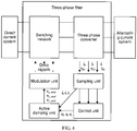
- FIG. 4 shows a three-phase converter 200 in an embodiment of the present invention.
- the three-phase converter 200 is connected between a direct current system 100 and an alternating current system 300.
- the three-phase converter 200 includes a switching network 201, a three-phase filter 202 connected to the switching network 201, a sampling unit 203 connected to the three-phase filter 202, a control unit 204 connected to the three-phase sampling unit 203, an active damping unit 205 connected to both the control unit 204 and the sampling unit 203, and a modulation unit 206 connected between the active damping unit 205 and the switching network 201.
- the active damping unit 205 determines a regulation component of each phase circuit according to different statuses of phase currents of three-phase currents in the three-phase filter 202; superposes the regulation component of each phase circuit with the three-phase modulated waves generated by the control unit 204, to generate corrected three-phase modulated waves; and then uses the corrected three-phase modulated waves to control the switching transistor of the switching network 201, thereby reducing the common-mode current of the three-phase converter 200.
- the foregoing direct current system 100 may be any power source that provides a direct current, and includes a battery, a solar photovoltaic panel, or the like.
- the foregoing alternating current system 300 may be any device or apparatus that requires alternating current input, and includes a power grid, a motor, or the like.
- An input end of the foregoing switching network 201 is connected to an output end of the direct current system 100.
- the switching network 201 is configured to convert the direct current of the direct current system 100 into a three-level alternating current output.
- the three-phase filter 202 is configured to convert the multi-level alternating current output of the switching network 201 into an alternating current having a sinusoidal or cosine waveform, so as to be transmitted to the alternating current system 300.
- the foregoing sampling unit 203 is configured to: obtain voltage and current signals in a hardware system, convert the voltage and current signals into a digital signal that is convenient for processing by the control unit 204, and output the digital signal to the control unit 204.
- the sampling unit 203 is specifically configured to: obtain three-phase currents and voltages in the three-phase filter 202 and separately perform sampling and measurement, to obtain three-phase currents i a , i b , and i c and three-phase voltages v ga , v gb , and v gc ; and provide the three-phase currents and voltages to the control unit 204 and the active damping unit 205.
- the foregoing control unit 204 is configured to: perform comparative calculation on sampled and converted voltage and current signals and a set reference value, perform corresponding signal processing, and output modulated waves.
- the control unit 204 is specifically configured to perform discontinuous pulse-width modulation (DPWM) according to the input three-phase currents i a , i b , and i c and three-phase voltages v ga , v gb , and v gc , to obtain modulated waves v a , v b , and v c .
- DPWM discontinuous pulse-width modulation
- the control unit 204 transfers the modulated waves v a , v b , and v c to the active damping unit 205.
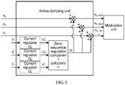
- the foregoing active damping unit 205 is configured to: perform independent regulation on the three-phase currents i a , i b , and i c respectively by using mutually independent regulation functions to obtain regulation components v' a , v ' b , and v ' c that are in a one-to-one correspondence with the three-phase currents i a , i b , and i c , obtain a zero-sequence regulation component v 0 according to the regulation components v ' a , v ' b , and v ' c , separately add the zero-sequence regulation component v 0 to the three-phase modulated waves v a , v b , and v c that are output by the control unit 204 to obtain new three-phase modulated waves v a_mod , v b_mod , and v c_mod , and transmit the new three-phase modulated waves v a
- the foregoing active damping unit 205 includes a current regulator G a , a current regulator G b , a current regulator G c , and a zero-sequence regulation component calculator 2050.
- the current regulator G a , the current regulator G b , and the current regulator G c respectively receive, in a one-to-one correspondence, the three-phase currents i a , i b , and i c that are transferred by the sampling unit 203, respectively regulate the three-phase currents i a , i b , and i c by using the mutually independent regulation functions, and respectively output the regulation components v' a , v ' b , and v ' c to the zero-sequence regulation component calculator 2050.
- PI proportional integral
- PR proportional resonant
- the current regulator may be a regulator of another form, and correspondingly use a different regulation function.
- two or more types of regulators may be used in combination. The following lists some current regulators included in the present invention, but the present invention is not limited thereto.
- parameters represented by a same symbol have a same meaning. For the purpose of brevity, a parameter is described only at the first appearance.
- the current regulator may be a derivative regulator, and a regulation function G of the derivative regulator is:
- the three-phase current regulators in the active damping unit 205 may be set to different values, to respectively perform independent modulation on the three-phase currents and perform system correction in a control loop, so that an output can match a control loop of an existing symmetric system.
- An effect of the three-phase current regulators is an effect of added active damping.
- the regulation functions of the current regulators may be used as the regulation functions of the added virtual damping loop, where inputs are the currents, and outputs are the voltages, that is, the regulation components.
- the zero-sequence regulation component calculator 2050 receives the regulation components v' a , v ' b , and v ' c that are respectively output by the current regulator G a , the current regulator G b , and the current regulator G c , and calculates an average or a weighted average of the regulation components v' a , v ' b , and v ' c , where a result of the average or the weighted average is equal to the zero-sequence regulation component v 0 .
- the weighted average needs to be obtained by performing weighted averaging by using some weighting coefficients.
- the active damping unit 205 separately adds the zero-sequence regulation component v 0 to the three-phase modulated waves v a , v b , and v c that are output by the control unit 204 to obtain the new three-phase modulated waves v a_mod , v b_mod , and v c_mod , and transmits the new three-phase modulated waves v a_mod , v b_mod , and v c_mod to the modulation unit 206.
- the foregoing modulation unit 206 is configured to: compare the three-phase modulated waves with a carrier signal according to the modulated waves that are output by the control unit 204 and switch configuration in the hardware system, and output drive signals corresponding to switching devices.
- the modulation unit 206 is specifically configured to modulate the new three-phase modulated waves v a_mod , v b_mod , and v c_mod into drive signals of the switching network 201, to drive the switching network 201 to work.
- the foregoing three-phase converter 200 controls the switching network 201 by using the new three-phase modulated waves v a_mod , v b_mod , and v c_mod that are obtained through regulation by using the zero-sequence regulation component v 0 , to effectively suppress common-mode current resonance on the basis of original control by using the three-phase modulated waves v a , v b , and v c that are output by the control unit 204.
- the zero-sequence regulation component v 0 may be used to perform dynamic regulation in real time according to an entire three-phase system and a variation of the three-phase currents i a , i b , and i c , to cancel excited oscillation of common-mode current resonance caused by a drastic variation of the three-phase currents i a , i b , and i c , thereby ensuring stable and efficient operation of the three-phase system.
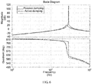
- a solid line depicts a Bode plot of a common-mode voltage to common-mode current regulation function of an active damping system in an embodiment of the present invention
- a dotted line depicts a Bode plot of a common-mode voltage to common-mode current regulation function of a damping-free system.
- a Bode plot is a method for illustrating a frequency response of a system.
- a Bode plot includes a magnitude plot (upper) and a phase plot (lower). Horizontal coordinates in both plots are drawn according to logarithmic scales of frequencies.
- a unit of a vertical coordinate in the magnitude plot is decibel (dB).
- the vertical coordinate represents an amplification factor of a common-mode current amplitude relative to a common-mode voltage amplitude, a larger value indicates a greater amplification factor.
- the three-phase converter in this embodiment of the present invention is applicable to various three-phase systems and is applicable to any system that needs three-phase input to drive switching devices.
- the three-phase converter is applicable to rectifier and inverter systems with two levels, three levels, five levels, or cascaded levels.
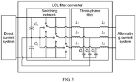
- switching network 201 In the various three-phase systems, other unit combinations, except the switching network 201, are the same and applicable. As shown in FIG. 7 , the following describes in detail a circuit structure of the switching network 201 by using an example in which a three-phase three-level inverter is applied to a photovoltaic inverter system.
- the switching network 201 includes a first voltage-dividing capacitor C1, a second voltage-dividing capacitor C2, a first switch combination Sa, a second switch combination Sb, and a third switch combination Sc.
- the first voltage-dividing capacitor C1 and the second voltage-dividing capacitor C2 are mutually connected in series between a positive electrode and a negative electrode of a direct current power source 100, and are configured to divide a voltage of the direct current power source 100.
- the first switch combination Sa, the second switch combination Sb, and the third switch combination Sc are mutually connected in parallel between the positive electrode and the negative electrode of the direct current power source 100.
- a series combination including the first voltage-dividing capacitor C1 and the second voltage-dividing capacitor C2 is connected in parallel to the first switch combination Sa, the second switch combination Sb, and the third switch combination Sc.
- the first switch combination Sa includes a first connection terminal Sa1 and a second connection terminal Sa2 that are respectively connected to the positive electrode and the negative electrode of the direct current power source, a third connection terminal Sa3 connected to a middle point of the series combination including the first voltage-dividing capacitor C1 and the second voltage-dividing capacitor C2, and a fourth connection terminal Sa4 connected to an input end of the three-phase filter.
- the second switch combination Sb includes a first connection terminal Sb1 and a second connection terminal Sb2 that are respectively connected to the positive electrode and the negative electrode of the direct current power source, a third connection terminal Sb3 connected to the middle point of the series combination including the first voltage-dividing capacitor C1 and the second voltage-dividing capacitor C2, and a fourth connection terminal Sb4 separately connected to three input ends of the three-phase filter.
- the third switch combination Sc includes a first connection terminal Sc1 and a second connection terminal Sc2 that are respectively connected to the positive electrode and the negative electrode of the direct current power source, a third connection terminal Sc3 connected to the middle point of the series combination including the first voltage-dividing capacitor C1 and the second voltage-dividing capacitor C2, and a fourth connection terminal Sc4 separately connected to the three input ends of the three-phase filter.
- the third connection terminals Sa3, Sb3, and Sc3 of the three switch combinations are respectively connected to the three input ends of the three-phase filter 202.
- Each of the fourth connection terminals Sa4, Sb4, and Sc4 is selectively connected to or disconnected from any one of the first, second, or third connection terminal of the switch combination to which the fourth connection terminal belongs, to implement conversion between the direct current and the alternating current.
- the fourth connection terminals Sa4, Sb4, and Sc4 selectively implement, by using disconnect and connect combinations of switching transistors in the switch combinations, the connection to or the disconnection from any one of the first, second, or third connection terminal of their respective switch combinations, to implement the conversion between the direct current and the alternating current.
- the three-phase filter 202 includes six inductors in three groups each including two inductors connected in series between the three fourth connection terminals Sa4, Sb4, and Sc4 of the switching network 201 and three input ends of the alternating current system 300; and includes three filtering capacitors C0 separately connected to the middle point of the series combination including the first voltage-dividing capacitor C1 and the second voltage-dividing capacitor C2 and respectively connected to middle points of the three groups of inductors each including two connected in series.
- the six inductors include a first converter-side inductor L1a, a second converter-side inductor L1b, a third converter-side inductor L1c, a first alternating current-side inductor L2a, a second alternating current-side inductor L2b, and a third alternating current-side inductor L2c.
- the first converter-side inductor L1a and the first alternating current-side inductor L2a are connected in series between the fourth connection terminal Sa4 of the first switch combination Sa and an input end of the alternating current system 300.
- the second converter-side inductor L1b and the second alternating current-side inductor L2b are connected in series between the fourth connection terminal Sb4 of the second switch combination Sb and an input end of the alternating current system 300.
- the third converter-side inductor L1c and the third alternating current-side inductor L2c are connected in series between the fourth connection terminal Sc4 of the third switch combination Sc and an input end of the alternating current system 300.
- One end of each of the filtering capacitors C0 is connected to the middle point of the series combination including the first voltage-dividing capacitor C1 and the second voltage-dividing capacitor C2, and the other end of each of the filtering capacitors C0 is connected to the middle point of one of the three groups of inductors.
- another embodiment of the present invention includes a three-phase converter control method.
- the method is implemented in one of the hardware environments in the foregoing embodiment.
- the method includes the following steps:
- an active damping unit of the three-phase converter receives the three-phase currents i a , i b , and i c that are obtained through sampling and detection and transferred by the sampling unit.
- the three-phase currents i a , i b , and i c are respectively input to corresponding current regulators G a , G b , and G c .
- Independent regulation functions on the current regulators are used to respectively regulate the three-phase currents i a , i b , and i c , and the regulation components v' a , v ' b , and v' c are separately output to a zero-sequence regulation component calculator of the active damping unit.
- the current regulators and regulation functions used in this embodiment of the present invention are the same as those in the foregoing embodiment. Details are not described herein again.
- the zero-sequence regulation component calculator receives the regulation components v' a , v ' b , and v ' c that are respectively output by the current regulator G a , the current regulator G b , and the current regulator G c , and calculates an average or a weighted average of the regulation components v' a , v ' b , and v ' c , where a result of the average or the weighted average is equal to the zero-sequence regulation component v 0 .
- the weighted average needs to be obtained by performing weighted averaging by using some weighting coefficients.
- an error exists in a process of measuring and processing a variable such as a current, affecting precision of a final value obtained through calculation.
- Overall calculation precision is related to all the following: precision of a measurement device, an ambient temperature, and processing precision of a digital processor. Errors are unavoidable and ubiquitous, such as a quantization error caused by discrete rounding when an analog signal is converted into a digital signal, or a temperature error caused because a resistivity of a semiconductor material in a Hall sensor varies according to temperatures.
- the active damping unit separately adds the zero-sequence regulation component v 0 to the three-phase modulated waves v a , v b , and v c that are output by a control unit of the three-phase converter, to obtain the new three-phase modulated waves v a_mod , v b_mod , and v c_mod , and transmit the new three-phase modulated waves v a_mod , v b_mod , and v c_mod to a modulation unit of the three-phase converter.
- the modulation unit is configured to: compare the three-phase modulated waves and the carrier signal according to the modulated waves that are output by the control unit and switch configuration in a hardware system, and output drive signals corresponding to the switching devices.
- the modulation unit is specifically configured to modulate the new three-phase modulated waves v a_mod , v b_mod , and v c_mod into drive signals of a switching network of the three-phase converter, to drive the switching network to work.
- a three-phase converter is applied to a photovoltaic system.
- the photovoltaic system includes a photovoltaic cell panel and the three-phase converter connected between the photovoltaic cell panel and an alternating current power grid.
- the three-phase converter is configured to: convert, into multiple levels by using switching devices, a direct current that is output by the photovoltaic cell panel; output three-phase currents i a , i b , and i c after performing filtering processing based on the multiple levels; and perform independent regulation on the three-phase currents i a , i b , and i c respectively by using mutually independent regulation functions, to obtain regulation components v' a , v ' b , and v' c .
- the three-phase converter obtains a zero-sequence regulation component v 0 through calculation according to the regulation components v' a , v ' b , and v' c ; separately adds the zero-sequence regulation component v 0 to three-phase modulated waves v a , v b , and v c , to obtain new three-phase modulated waves v a_mod , v b_mod , and v c_mod ; and finally compares the new three-phase modulated waves v a_mod , v b_mod , and v c_mod with a carrier signal of the three-phase converter, and outputs drive signals of switching devices of the three-phase converter, so as to convert, into an alternating current, the direct current that is output by the photovoltaic cell panel and input the alternating current to the alternating current power grid.
- the three-phase converter includes a current regulator G a , a current regulator Gb, and a current regulator G c .
- the current regulator G a , the current regulator G b , and the current regulator G c respectively receive the three-phase currents i a , i b , and i c in a one-to-one correspondence, and respectively regulate the three-phase currents i a , i b , and i c by using the mutually independent regulation functions, to obtain the regulation components v ' a , v ' b , and v ' c that are in a one-to-one correspondence with the three-phase currents i a , i b , and i c .
- the three-phase converter further includes a zero-sequence regulation component calculator.
- the zero-sequence regulation component calculator receives the regulation components v ' a , v ' b , and v ' c that are respectively output by the current regulator G a , the current regulator G b , and the current regulator G c , and calculates an average or a weighted average of the regulation components v' a , v ' b , and v ' c , where a result of the average or the weighted average is equal to the zero-sequence regulation component v 0 .
- compositional structures and circuit design of the foregoing three-phase converter are all the same as related content described in the foregoing embodiment of present invention. Details are not described herein.
- a three-phase converter is applied to an electric vehicle.
- a power system of the electric vehicle includes a direct current power source, a three-phase motor, and a three-phase converter connected between the direct current power source and the three-phase motor.
- the three-phase converter is configured to: convert, into multiple levels by using switching devices, a direct current that is output by the photovoltaic cell panel; and output three-phase currents i a , i b , and i c after performing filtering processing based on the multiple levels.
- the three-phase converter includes a current regulator G a , a current regulator G b , a current regulator G c , and a zero-sequence regulation component calculator.
- the current regulator G a , the current regulator G b , and the current regulator G c are configured to: respectively receive the three-phase currents i a , ib, and i c in a one-to-one correspondence, and perform independent regulation on the three-phase currents i a , i b , and i c respectively by using mutually independent regulation functions, to obtain regulation components v' a , v ' b , and v' c .
- the zero-sequence regulation component calculator receives the regulation components v' a , v ' b , and v ' c that are respectively output by the current regulator G a , the current regulator G b , and the current regulator G c , and calculates an average or a weighted average of the regulation components v' a , v ' b , and v ' c , where a result of the average or the weighted average is equal to a zero-sequence regulation component v 0 .
- the three-phase converter is further configured to: compare new three-phase modulated waves v a_mod , v b_mod , and v c_mod with a carrier signal of the three-phase converter, and output drive signals of switching devices of the three-phase converter, so as to convert, into an alternating current, the direct current that is output by the direct current power source and input the alternating current to the three-phase motor.
- compositional structures and circuit design of the foregoing three-phase converter are all the same as related content described in the foregoing embodiment of present invention. Details are not described herein.
Landscapes
- Engineering & Computer Science (AREA)
- Power Engineering (AREA)
- Inverter Devices (AREA)
- Ac-Ac Conversion (AREA)
Claims (12)
- Convertisseur triphasé (200), conçu pour être connecté entre un système à courant continu et un système à courant alternatif pour effectuer une interconversion entre un courant continu et un courant alternatif, le convertisseur triphasé (200) comprenant un réseau de commutation (201) qui est conçu pour convertir un courant continu en multiples niveaux, un filtre triphasé (202) qui est connecté au réseau de commutation (201) et qui délivre en sortie des courants triphasés ia, ib et ic sur la base des multiples niveaux, une unité d'échantillonnage (203) connectée au filtre triphasé (202), une unité de commande (20, 204) connectée à l'unité d'échantillonnage (203), une unité d'amortissement actif (205) connectée à la fois à l'unité de commande (20, 204) et à l'unité d'échantillonnage (203), et une unité de modulation (206) connectée entre l'unité d'amortissement active (205) et le réseau de commutation (201), l'unité d'échantillonnage (203) étant conçue pour :obtenir les courants triphasés ia, ib, et ic qui sont délivrés en sortie par le filtre triphasé (202), et envoyer les courants triphasés ia, ib, et ic à l'unité d'amortissement actif (205) ;l'unité d'amortissement actif (205) étant conçue pour :effectuer une régulation indépendante sur les courants triphasés ia, ib, et ic respectivement à l'aide de fonctions de régulation mutuellement indépendantes pour obtenir des composantes de régulation v'a, v'b et v'c qui sont en correspondance biunivoque avec les courants triphasés ia, ib, et ic , obtenir une composante de régulation homopolaire vo en fonction des composantes de régulation v'a, v'b, et v'c, superposer séparément la composante de régulation homopolaire vo avec des ondes modulées triphasées va, vb, et vc qui sont délivrées en sortie par l'unité de commande (20, 204) pour obtenir de nouvelles ondes modulées triphasées v a_mod, v b_mod, and v c_mod, et transmettre les nouvelles ondes modulées triphasées v a_mod, v b_mod, et v c_mod à l'unité de modulation (206) ;l'unité de modulation (206) étant conçue pour moduler les nouvelles ondes modulées triphasées v a_mod, v b_mod, et v c_mod en signaux de pilotage du réseau de commutation (201), pour piloter le réseau de commutation (201) afin de délivrer en sortie les multiples niveaux au filtre triphasé (202) ; etle filtre triphasé (202) étant conçu pour convertir les multiples niveaux en un courant alternatif qui est entré dans le système à courant alternatif, l'unité d'amortissement actif (205) comprenant un régulateur de courant Ga, un régulateur de courant Gb et un régulateur de courant Gc ; etle régulateur de courant Ga, le régulateur de courant Gb et le régulateur de courant Gc recevant respectivement les courants triphasés ia, ib, et ic dans une correspondance biunivoque, et régulant les courants triphasés ia, ib, et ic respectivement à l'aide des fonctions de régulation mutuellement indépendantes, pour obtenir les composantes de régulation v'a, v'b, et v'c qui sont dans une correspondance biunivoque avec les courants triphasés ia, ib, et ic; etcaractérisé en ce que l'unité d'amortissement actif (205) comprend en outre un calculateur de composante de régulation homopolaire (2050) ; etle calculateur de composante de régulation homopolaire (2050) reçoit les composantes de régulation v'a, v'b , et v'c qui sont respectivement délivrées en sortie par le régulateur de courant Ga, le régulateur de courant Gb et le régulateur de courant Gc, et calcule une moyenne ou une moyenne pondérée des composantes de régulation v'a, v'b, and v'c, un résultat de la moyenne ou de la moyenne pondérée étant la composante de régulation homopolaire vo .
- Convertisseur triphasé (200) selon la revendication 1, dans lequel au moins un élément parmi le régulateur de courant Ga, le régulateur de courant Gb ou le régulateur de courant Gc est un régulateur proportionnel intégral (PI) et une fonction de régulation G du régulateur PI est :

- Convertisseur triphasé (200) selon la revendication 1, dans lequel au moins un élément parmi le régulateur de courant Ga, le régulateur de courant Gb ou le régulateur de courant Gc est un régulateur proportionnel résonant (PR) et une fonction de régulation G du régulateur PR est :

- Convertisseur triphasé (200) selon la revendication 1, dans lequel au moins un élément parmi le régulateur de courant Ga, le régulateur de courant Gb ou le régulateur de courant Gc est un régulateur de dérivé et une fonction de régulation G du régulateur de dérivé est :
G = Ks, où G=v'a /ia =v'b /ib =v'c /ic, K est un coefficient de proportionnalité, et s est une fréquence complexe dans laquelle une fréquence et une phase d'un signal d'entrée sont représentées à l'aide d'un nombre complexe. - Convertisseur triphasé (200) selon la revendication 1, dans lequel au moins un élément parmi le régulateur de courant Ga, le régulateur de courant Gb ou le régulateur de courant Gc est un filtre passe-haut, et une fonction de régulation G du filtre passe-haut est :

- Convertisseur triphasé (200) selon la revendication 1, dans lequel au moins un élément parmi le régulateur de courant Ga, le régulateur de courant Gb ou le régulateur de courant Gc est un régulateur d'avance-retard et une fonction de régulation G du régulateur d'avance-retard est :

- Convertisseur triphasé (200) selon la revendication 1, dans lequel au moins un élément parmi le régulateur de courant Ga, le régulateur de courant Gb ou le régulateur de courant Gc est un régulateur intégral généralisé de second ordre, et une fonction de régulation G du régulateur intégral généralisé de second ordre est :
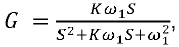
- Convertisseur triphasé (200) selon la revendication 1, dans lequel au moins un élément parmi le régulateur de courant Ga, le régulateur de courant Gb ou le régulateur de courant Gc est un régulateur de placement de pôle-zéro, et une fonction de régulation G du régulateur de placement de pôle-zéro est :

- Convertisseur triphasé (200) selon l'une quelconque des revendications 1 à 8, dans lequel le réseau de commutation (201) comprend un premier condensateur de division de tension C1, un second condensateur de division de tension C2, une première combinaison de commutateurs Sa, une deuxième combinaison de commutateurs Sb et une troisième combinaison de commutateurs Sc, le premier condensateur de division de tension C1 et le second condensateur de division de tension C2 étant mutuellement connectés en série entre une électrode positive et une électrode négative d'une source d'alimentation en courant continu, et étant conçus pour diviser une tension de la source d'alimentation en courant continu ;la première combinaison de commutateurs Sa, la deuxième combinaison de commutateurs Sb et la troisième combinaison de commutateurs Sc sont mutuellement connectées en parallèle entre l'électrode positive et l'électrode négative de la source d'alimentation en courant continu ; etune combinaison en série comprenant le premier condensateur de division de tension C1 et le second condensateur de division de tension C2 est connectée en parallèle à la première combinaison de commutateurs Sa, à la deuxième combinaison de commutateurs Sb et à la troisième combinaison de commutateurs Sc.
- Convertisseur triphasé (200) selon la revendication 9, dans lequel la première combinaison de commutateurs Sa comprend une première borne de connexion Sa1 et une deuxième borne de connexion Sa2 qui sont respectivement connectées à l'électrode positive et à l'électrode négative de la source d'alimentation en courant continu, une troisième borne de connexion Sa3 connectée à un point médian de la combinaison en série comprenant le premier condensateur de division de tension C1 et le second condensateur de division de tension C2, et une quatrième borne de connexion Sa4 connectée à une extrémité d'entrée du filtre triphasé (202) ;la deuxième combinaison de commutateurs Sb comprend une première borne de connexion Sb1 et une deuxième borne de connexion Sb2 qui sont respectivement connectées à l'électrode positive et à l'électrode négative de la source d'alimentation en courant continu, une troisième borne de connexion Sb3 connectée au point médian de la combinaison en série comprenant le premier condensateur de division de tension C1 et le second condensateur de division de tension C2, et une quatrième borne de connexion Sb4 connectée à une extrémité d'entrée du filtre triphasé (202) ;la troisième combinaison de commutateurs Sc comprend une première borne de connexion Sc1 et une deuxième borne de connexion Sc2 qui sont respectivement connectées à l'électrode positive et à l'électrode négative de la source d'alimentation en courant continu, une troisième borne de connexion Sc3 connectée au point médian de la combinaison en série comprenant le premier condensateur de division de tension C1 et le second condensateur de division de tension C2, et une quatrième borne de connexion Sc4 connectée séparément aux trois extrémités d'entrée du filtre triphasé (202) ; etchacune des quatrièmes bornes de connexion Sa4, Sb4 et Sc4 est sélectivement connectée à ou déconnectée de l'une quelconque des première, deuxième ou troisième bornes de connexion de la combinaison de commutateurs à laquelle appartient la quatrième borne de connexion, pour mettre en œuvre la conversion entre le courant continu et le courant alternatif.
- Procédé de commande d'un convertisseur triphasé (200), utilisé pour commander un convertisseur triphasé (200) connecté entre un système à courant continu et un système à courant alternatif pour effectuer une interconversion entre un courant continu et un courant alternatif, le procédé comprenant :étape 101 : l'obtention de courants triphasés ia, ib, et ic dans le convertisseur triphasé (200), et la réalisation d'une régulation indépendante sur les courants triphasés ia, ib, et ic respectivement à l'aide de fonctions de régulation mutuellement indépendantes, pour obtenir les composantes de régulation v'a, v'b, et v'c qui sont dans une correspondance biunivoque avec les courants triphasés ia, ib, et ic;étape 102 : l'obtention d'une composante de régulation homopolaire vo par le biais d'un calcul en fonction des composantes de régulation v'a, v'b, et v'c ;étape 103 : l'ajout séparé de la composante de régulation homopolaire v0 à des ondes modulées triphasées va, vb, et vc, pour obtenir de nouvelles ondes modulées triphasées v a_mod, v b_mod et v c_mod ; etétape 104 : la comparaison des nouvelles ondes modulées triphasées v a_mod, v b_mod, et v c_mod avec un signal de porteuse du convertisseur triphasé (200), et le fait de délivrer en sortie des signaux de pilotage de dispositifs de commutation du convertisseur triphasé (200), caractérisé en ce que l'obtention d'une composante de régulation homopolaire vo par le biais d'un calcul en fonction des composantes de régulation v'a, v'b, et v'c comprend :
le calcul d'une moyenne ou d'une moyenne pondérée des composantes de régulation v'a, v'b, et v'c, un résultat de la moyenne ou de la moyenne pondérée étant la composante de régulation homopolaire vo . - Procédé de commande de convertisseur triphasé (200) selon la revendication 11, selon lequel l'obtention d'une composante de régulation homopolaire vo par le biais d'un calcul en fonction des composantes de régulation v'a, v'b, et v'c comprend :
le calcul d'une moyenne pondérée des composantes de régulation v'a, v'b, et v'c, pour obtenir la composante de régulation homopolaire vo, une formule de calcul étant : Composante de régulation homopolaire,
Applications Claiming Priority (1)
| Application Number | Priority Date | Filing Date | Title |
|---|---|---|---|
| PCT/CN2016/101258 WO2018058603A1 (fr) | 2016-09-30 | 2016-09-30 | Convertisseur triphasé et son procédé de commande |
Publications (3)
| Publication Number | Publication Date |
|---|---|
| EP3514939A1 EP3514939A1 (fr) | 2019-07-24 |
| EP3514939A4 EP3514939A4 (fr) | 2019-10-16 |
| EP3514939B1 true EP3514939B1 (fr) | 2021-07-28 |
Family
ID=61763014
Family Applications (1)
| Application Number | Title | Priority Date | Filing Date |
|---|---|---|---|
| EP16917353.1A Active EP3514939B1 (fr) | 2016-09-30 | 2016-09-30 | Convertisseur triphasé et son procédé de commande |
Country Status (6)
| Country | Link |
|---|---|
| US (1) | US10715056B2 (fr) |
| EP (1) | EP3514939B1 (fr) |
| JP (1) | JP6710810B2 (fr) |
| CN (2) | CN109792219B (fr) |
| BR (1) | BR112019005998B1 (fr) |
| WO (1) | WO2018058603A1 (fr) |
Families Citing this family (24)
| Publication number | Priority date | Publication date | Assignee | Title |
|---|---|---|---|---|
| CN106981976B (zh) * | 2017-03-24 | 2019-08-20 | 江苏固德威电源科技股份有限公司 | T型三电平三相逆变器抑制中线共模电流的方法 |
| JP7008222B2 (ja) * | 2017-04-24 | 2022-01-25 | パナソニックIpマネジメント株式会社 | 電力変換システム |
| US11329573B2 (en) * | 2017-08-04 | 2022-05-10 | Panasonic Intellectual Property Management Co., Ltd. | Power converter and power conversion system |
| CN107994796B (zh) * | 2017-12-26 | 2020-04-28 | 华为技术有限公司 | 单相变流器的控制方法以及装置 |
| CN108429282B (zh) * | 2018-03-28 | 2020-11-10 | 阳光电源股份有限公司 | 一种中高压光伏发电系统 |
| KR102409013B1 (ko) * | 2018-10-30 | 2022-06-14 | 도시바 미쓰비시덴키 산교시스템 가부시키가이샤 | 전력 변환 장치 |
| CN110350577A (zh) * | 2019-06-25 | 2019-10-18 | 陕西科技大学 | 基于qpci控制的三相并网逆变器控制系统和方法 |
| US11177660B2 (en) * | 2020-01-27 | 2021-11-16 | Mitsubishi Electric Power Products, Inc. | System and method for power converter control for virtual impedance |
| US11374517B2 (en) | 2020-09-21 | 2022-06-28 | Global Mixed-Mode Technology Inc. | Motor controller |
| TWI777247B (zh) * | 2020-09-21 | 2022-09-11 | 致新科技股份有限公司 | 馬達控制器 |
| US11336206B2 (en) * | 2020-09-23 | 2022-05-17 | Rockwell Automation Technoligies, Inc. | Switching frequency and PWM control to extend power converter lifetime |
| CN112217409B (zh) * | 2020-11-05 | 2024-06-11 | 武汉理工大学 | 三相四桥臂电压型逆变器的变载波脉宽调制系统及方法 |
| CN112701725B (zh) * | 2020-12-22 | 2022-04-12 | 华中科技大学 | 一种混合导通模式的并网逆变器 |
| CN112821790B (zh) * | 2021-01-04 | 2022-08-12 | 台达电子企业管理(上海)有限公司 | 三相变换器及其控制方法 |
| EP4120528A1 (fr) | 2021-07-16 | 2023-01-18 | Siemens Aktiengesellschaft | Convertisseur de puissance |
| CN113556053B (zh) * | 2021-07-21 | 2022-10-28 | 华为数字能源技术有限公司 | 三相多电平逆变器的控制方法以及逆变器系统 |
| CN113644835B (zh) * | 2021-08-11 | 2023-03-24 | 上海儒竞智控技术有限公司 | 脉冲宽度调制方法、存储介质、电子设备及逆变电路 |
| CN114337439B (zh) * | 2021-12-09 | 2024-08-06 | 合肥工业大学 | 三相逆变器lcl滤波器的主动阻尼共同解耦方法及装置 |
| US11742744B1 (en) | 2022-03-01 | 2023-08-29 | Lunar Energy, Inc. | Dynamic adjustment of damping of a filter of an inverter |
| CN114301267B (zh) * | 2022-03-09 | 2022-05-24 | 深圳市首航新能源股份有限公司 | 开关管的驱动方法及装置、逆变器 |
| CN115378286A (zh) * | 2022-08-19 | 2022-11-22 | 兴储世纪科技(深圳)有限公司 | 一种三相三电平变流器电路及其调制方法 |
| CN115603364A (zh) * | 2022-10-19 | 2023-01-13 | 华为数字能源技术有限公司(Cn) | 并网逆变装置以及并网控制方法 |
| CN118393328B (zh) * | 2024-06-27 | 2024-09-03 | 锦浪科技股份有限公司 | 故障判断方法、装置及一种逆变器电路 |
| EP4730629A1 (fr) * | 2024-10-18 | 2026-04-22 | Volvo Penta Corporation | Convertisseurs de puissance à boucle de mode commun |
Family Cites Families (11)
| Publication number | Priority date | Publication date | Assignee | Title |
|---|---|---|---|---|
| US5378979A (en) * | 1992-11-25 | 1995-01-03 | Allen-Bradley Company, Inc. | Method and apparatus for efficiently computing symmetric sequence signals in a three phase power system |
| US6950321B2 (en) * | 2003-09-24 | 2005-09-27 | General Motors Corporation | Active damping control for L-C output filters in three phase four-leg inverters |
| CN101753044B (zh) * | 2010-01-26 | 2012-06-27 | 北方工业大学 | 一种基于零序电压注入的三电平中点电位平衡控制方法 |
| US8760106B2 (en) * | 2011-03-30 | 2014-06-24 | Bose Corporation | Common mode hysteresis for pulse-width modulation drives |
| ES2718807T3 (es) * | 2012-06-07 | 2019-07-04 | Abb Research Ltd | Procedimiento de amortiguación de secuencia cero y equilibrado de tensión en un convertidor de tres niveles con condensadores de enlace de CC divididos y filtro LCL virtualmente conectado a tierra |
| CN103023070B (zh) * | 2012-12-31 | 2014-12-10 | 山东大学 | 基于3d-spwm的混合箝位式三电平三相四线制光伏系统 |
| KR101928437B1 (ko) * | 2013-01-14 | 2018-12-12 | 삼성전자주식회사 | 전동기를 구동하는 인버터의 출력전압을 제어하는 방법 및 장치. |
| CN103414363B (zh) * | 2013-08-30 | 2016-03-30 | 阳光电源股份有限公司 | 一种三相三电平变换器电容电位平衡控制方法及系统 |
| CN104065292B (zh) * | 2014-06-26 | 2016-08-31 | 许继集团有限公司 | 三电平变换器中点电位平衡控制方法与装置 |
| JP6316152B2 (ja) * | 2014-09-16 | 2018-04-25 | シャープ株式会社 | パワーコンディショナ |
| CN105207455A (zh) | 2015-09-10 | 2015-12-30 | 艾思玛新能源技术(上海)有限公司苏州高新区分公司 | 一种逆变器的谐波抑制方法及装置 |
-
2016
- 2016-09-30 BR BR112019005998-9A patent/BR112019005998B1/pt active IP Right Grant
- 2016-09-30 WO PCT/CN2016/101258 patent/WO2018058603A1/fr not_active Ceased
- 2016-09-30 JP JP2019517335A patent/JP6710810B2/ja active Active
- 2016-09-30 EP EP16917353.1A patent/EP3514939B1/fr active Active
- 2016-09-30 CN CN201680089782.8A patent/CN109792219B/zh active Active
- 2016-09-30 CN CN202111439583.4A patent/CN115940680A/zh active Pending
-
2019
- 2019-03-29 US US16/369,828 patent/US10715056B2/en active Active
Non-Patent Citations (1)
| Title |
|---|
| QIANG SONG ET AL: "A neutral-point potential balancing algorithm for three-level NPC inverters using analytically injected zero-sequence voltage", APEC 2003. 18TH. ANNUAL IEEE APPLIED POWER ELECTRONICS CONFERENCE AND EXPOSITION. MIAMI BEACH, FL, FEB. 9 - 13, 2003; [ANNUAL APPLIED POWER ELECTRONICS CONFERENCE], NEW YORK, NY : IEEE, US, 9 February 2003 (2003-02-09), pages 228 - 233vol.1, XP032155906, ISBN: 978-0-7803-7768-4, DOI: 10.1109/APEC.2003.1179220 * |
Also Published As
| Publication number | Publication date |
|---|---|
| EP3514939A4 (fr) | 2019-10-16 |
| JP2019530418A (ja) | 2019-10-17 |
| WO2018058603A1 (fr) | 2018-04-05 |
| JP6710810B2 (ja) | 2020-06-17 |
| BR112019005998A2 (pt) | 2019-06-25 |
| CN115940680A (zh) | 2023-04-07 |
| US20190229646A1 (en) | 2019-07-25 |
| BR112019005998B1 (pt) | 2023-04-18 |
| CN109792219A (zh) | 2019-05-21 |
| US10715056B2 (en) | 2020-07-14 |
| CN109792219B (zh) | 2021-12-03 |
| EP3514939A1 (fr) | 2019-07-24 |
Similar Documents
| Publication | Publication Date | Title |
|---|---|---|
| EP3514939B1 (fr) | Convertisseur triphasé et son procédé de commande | |
| Pan et al. | Voltage balancing control of diode-clamped multilevel rectifier/inverter systems | |
| KR101512188B1 (ko) | 모듈형 멀티레벨 컨버터의 구동방법 및 구동장치 | |
| EP3537589B1 (fr) | Procédé de modulation d'impulsions en durée, système de modulation d'impulsions en durée, et contrôleur | |
| Xiao et al. | Virtual flux direct power control for PWM rectifiers based on an adaptive sliding mode observer | |
| CN103701350A (zh) | 低频工况下模块化多电平变流器电容电压波动抑制方法 | |
| EP4030611B1 (fr) | Procédé et dispositif de commande pour onduleur connecté au réseau | |
| Lei et al. | An improved virtual resistance damping method for grid-connected inverters with LCL filters | |
| Kato et al. | Lyapunov-based digital control of a grid-connected inverter with an LCL filter | |
| CN107994796B (zh) | 单相变流器的控制方法以及装置 | |
| CN107896071A (zh) | 一种基于神经网络的三相组合式逆变电源 | |
| Maheshwari et al. | A novel high bandwidth current control strategy for SiC MOSFET based active front-end rectifiers under unbalanced input voltage conditions | |
| Xiao et al. | A novel current controller for grid-connected voltage-source-inverters | |
| Dai et al. | Design considerations of coupling inductance for active power filters | |
| CN118174582A (zh) | 一种无差拍预测控制方法 | |
| CN113489055B (zh) | 一种改进的弱电网下三相电流源型并网逆变器电网电压前馈方法 | |
| Dong et al. | Input Voltage Proportional Feedforward Control for Three-Phase Buck Rectifier Under Unbalanced Input Voltages and Wide AC Input Frequency | |
| Sun et al. | Quality management of energy storage VSG based on odd-order repetitive control | |
| CN210608909U (zh) | 一种基于自适应电流谐波抑制的逆变器电流控制系统 | |
| Tan et al. | Deadbeat plus fractional-order repetitive control for grid-tied inverter | |
| Deng et al. | A model-free predictive control of an isolated AC/DC matrix converter | |
| CN115459553B (zh) | 一种t型三电平pwm整流器中点电位spwm控制方法 | |
| RU212745U1 (ru) | Устройство подавления высших гармоник и коррекции коэффициента мощности сети | |
| CN120956090B (zh) | 一种三电平变流器的母线中点电压直流偏置消除方法 | |
| Hu et al. | Asymmetrical Interleaved Switching Power Amplifier Based on Arm Multiplexing |
Legal Events
| Date | Code | Title | Description |
|---|---|---|---|
| STAA | Information on the status of an ep patent application or granted ep patent |
Free format text: STATUS: THE INTERNATIONAL PUBLICATION HAS BEEN MADE |
|
| PUAI | Public reference made under article 153(3) epc to a published international application that has entered the european phase |
Free format text: ORIGINAL CODE: 0009012 |
|
| STAA | Information on the status of an ep patent application or granted ep patent |
Free format text: STATUS: REQUEST FOR EXAMINATION WAS MADE |
|
| 17P | Request for examination filed |
Effective date: 20190415 |
|
| AK | Designated contracting states |
Kind code of ref document: A1 Designated state(s): AL AT BE BG CH CY CZ DE DK EE ES FI FR GB GR HR HU IE IS IT LI LT LU LV MC MK MT NL NO PL PT RO RS SE SI SK SM TR |
|
| AX | Request for extension of the european patent |
Extension state: BA ME |
|
| A4 | Supplementary search report drawn up and despatched |
Effective date: 20190918 |
|
| RIC1 | Information provided on ipc code assigned before grant |
Ipc: H02M 7/5395 20060101ALI20190912BHEP Ipc: H02M 1/00 20060101ALN20190912BHEP Ipc: H02M 7/5387 20070101ALI20190912BHEP Ipc: H02M 1/12 20060101ALN20190912BHEP Ipc: H02P 27/08 20060101ALI20190912BHEP Ipc: H02M 7/487 20070101AFI20190912BHEP |
|
| DAV | Request for validation of the european patent (deleted) | ||
| DAX | Request for extension of the european patent (deleted) | ||
| STAA | Information on the status of an ep patent application or granted ep patent |
Free format text: STATUS: EXAMINATION IS IN PROGRESS |
|
| 17Q | First examination report despatched |
Effective date: 20200604 |
|
| GRAP | Despatch of communication of intention to grant a patent |
Free format text: ORIGINAL CODE: EPIDOSNIGR1 |
|
| STAA | Information on the status of an ep patent application or granted ep patent |
Free format text: STATUS: GRANT OF PATENT IS INTENDED |
|
| RIC1 | Information provided on ipc code assigned before grant |
Ipc: H02M 1/00 20060101ALN20210209BHEP Ipc: H02M 1/12 20060101ALN20210209BHEP Ipc: H02M 7/5395 20060101ALI20210209BHEP Ipc: H02M 7/487 20070101AFI20210209BHEP Ipc: H02P 27/08 20060101ALI20210209BHEP Ipc: H02M 7/5387 20070101ALI20210209BHEP |
|
| RIC1 | Information provided on ipc code assigned before grant |
Ipc: H02M 7/487 20070101AFI20210218BHEP Ipc: H02M 1/00 20060101ALN20210218BHEP Ipc: H02M 1/12 20060101ALN20210218BHEP Ipc: H02P 27/08 20060101ALI20210218BHEP Ipc: H02M 7/5395 20060101ALI20210218BHEP Ipc: H02M 7/5387 20070101ALI20210218BHEP |
|
| INTG | Intention to grant announced |
Effective date: 20210310 |
|
| GRAS | Grant fee paid |
Free format text: ORIGINAL CODE: EPIDOSNIGR3 |
|
| GRAA | (expected) grant |
Free format text: ORIGINAL CODE: 0009210 |
|
| STAA | Information on the status of an ep patent application or granted ep patent |
Free format text: STATUS: THE PATENT HAS BEEN GRANTED |
|
| AK | Designated contracting states |
Kind code of ref document: B1 Designated state(s): AL AT BE BG CH CY CZ DE DK EE ES FI FR GB GR HR HU IE IS IT LI LT LU LV MC MK MT NL NO PL PT RO RS SE SI SK SM TR |
|
| REG | Reference to a national code |
Ref country code: GB Ref legal event code: FG4D |
|
| REG | Reference to a national code |
Ref country code: CH Ref legal event code: EP |
|
| REG | Reference to a national code |
Ref country code: DE Ref legal event code: R096 Ref document number: 602016061436 Country of ref document: DE |
|
| REG | Reference to a national code |
Ref country code: AT Ref legal event code: REF Ref document number: 1415626 Country of ref document: AT Kind code of ref document: T Effective date: 20210815 |
|
| REG | Reference to a national code |
Ref country code: IE Ref legal event code: FG4D |
|
| REG | Reference to a national code |
Ref country code: LT Ref legal event code: MG9D |
|
| REG | Reference to a national code |
Ref country code: NL Ref legal event code: MP Effective date: 20210728 |
|
| REG | Reference to a national code |
Ref country code: AT Ref legal event code: MK05 Ref document number: 1415626 Country of ref document: AT Kind code of ref document: T Effective date: 20210728 |
|
| PG25 | Lapsed in a contracting state [announced via postgrant information from national office to epo] |
Ref country code: HR Free format text: LAPSE BECAUSE OF FAILURE TO SUBMIT A TRANSLATION OF THE DESCRIPTION OR TO PAY THE FEE WITHIN THE PRESCRIBED TIME-LIMIT Effective date: 20210728 Ref country code: FI Free format text: LAPSE BECAUSE OF FAILURE TO SUBMIT A TRANSLATION OF THE DESCRIPTION OR TO PAY THE FEE WITHIN THE PRESCRIBED TIME-LIMIT Effective date: 20210728 Ref country code: ES Free format text: LAPSE BECAUSE OF FAILURE TO SUBMIT A TRANSLATION OF THE DESCRIPTION OR TO PAY THE FEE WITHIN THE PRESCRIBED TIME-LIMIT Effective date: 20210728 Ref country code: PT Free format text: LAPSE BECAUSE OF FAILURE TO SUBMIT A TRANSLATION OF THE DESCRIPTION OR TO PAY THE FEE WITHIN THE PRESCRIBED TIME-LIMIT Effective date: 20211129 Ref country code: NL Free format text: LAPSE BECAUSE OF FAILURE TO SUBMIT A TRANSLATION OF THE DESCRIPTION OR TO PAY THE FEE WITHIN THE PRESCRIBED TIME-LIMIT Effective date: 20210728 Ref country code: NO Free format text: LAPSE BECAUSE OF FAILURE TO SUBMIT A TRANSLATION OF THE DESCRIPTION OR TO PAY THE FEE WITHIN THE PRESCRIBED TIME-LIMIT Effective date: 20211028 Ref country code: LT Free format text: LAPSE BECAUSE OF FAILURE TO SUBMIT A TRANSLATION OF THE DESCRIPTION OR TO PAY THE FEE WITHIN THE PRESCRIBED TIME-LIMIT Effective date: 20210728 Ref country code: AT Free format text: LAPSE BECAUSE OF FAILURE TO SUBMIT A TRANSLATION OF THE DESCRIPTION OR TO PAY THE FEE WITHIN THE PRESCRIBED TIME-LIMIT Effective date: 20210728 Ref country code: BG Free format text: LAPSE BECAUSE OF FAILURE TO SUBMIT A TRANSLATION OF THE DESCRIPTION OR TO PAY THE FEE WITHIN THE PRESCRIBED TIME-LIMIT Effective date: 20211028 Ref country code: RS Free format text: LAPSE BECAUSE OF FAILURE TO SUBMIT A TRANSLATION OF THE DESCRIPTION OR TO PAY THE FEE WITHIN THE PRESCRIBED TIME-LIMIT Effective date: 20210728 Ref country code: SE Free format text: LAPSE BECAUSE OF FAILURE TO SUBMIT A TRANSLATION OF THE DESCRIPTION OR TO PAY THE FEE WITHIN THE PRESCRIBED TIME-LIMIT Effective date: 20210728 |
|
| PG25 | Lapsed in a contracting state [announced via postgrant information from national office to epo] |
Ref country code: PL Free format text: LAPSE BECAUSE OF FAILURE TO SUBMIT A TRANSLATION OF THE DESCRIPTION OR TO PAY THE FEE WITHIN THE PRESCRIBED TIME-LIMIT Effective date: 20210728 Ref country code: LV Free format text: LAPSE BECAUSE OF FAILURE TO SUBMIT A TRANSLATION OF THE DESCRIPTION OR TO PAY THE FEE WITHIN THE PRESCRIBED TIME-LIMIT Effective date: 20210728 Ref country code: GR Free format text: LAPSE BECAUSE OF FAILURE TO SUBMIT A TRANSLATION OF THE DESCRIPTION OR TO PAY THE FEE WITHIN THE PRESCRIBED TIME-LIMIT Effective date: 20211029 |
|
| PG25 | Lapsed in a contracting state [announced via postgrant information from national office to epo] |
Ref country code: DK Free format text: LAPSE BECAUSE OF FAILURE TO SUBMIT A TRANSLATION OF THE DESCRIPTION OR TO PAY THE FEE WITHIN THE PRESCRIBED TIME-LIMIT Effective date: 20210728 |
|
| REG | Reference to a national code |
Ref country code: DE Ref legal event code: R097 Ref document number: 602016061436 Country of ref document: DE Ref country code: CH Ref legal event code: PL |
|
| REG | Reference to a national code |
Ref country code: BE Ref legal event code: MM Effective date: 20210930 |
|
| PG25 | Lapsed in a contracting state [announced via postgrant information from national office to epo] |
Ref country code: SM Free format text: LAPSE BECAUSE OF FAILURE TO SUBMIT A TRANSLATION OF THE DESCRIPTION OR TO PAY THE FEE WITHIN THE PRESCRIBED TIME-LIMIT Effective date: 20210728 Ref country code: SK Free format text: LAPSE BECAUSE OF FAILURE TO SUBMIT A TRANSLATION OF THE DESCRIPTION OR TO PAY THE FEE WITHIN THE PRESCRIBED TIME-LIMIT Effective date: 20210728 Ref country code: RO Free format text: LAPSE BECAUSE OF FAILURE TO SUBMIT A TRANSLATION OF THE DESCRIPTION OR TO PAY THE FEE WITHIN THE PRESCRIBED TIME-LIMIT Effective date: 20210728 Ref country code: MC Free format text: LAPSE BECAUSE OF FAILURE TO SUBMIT A TRANSLATION OF THE DESCRIPTION OR TO PAY THE FEE WITHIN THE PRESCRIBED TIME-LIMIT Effective date: 20210728 Ref country code: EE Free format text: LAPSE BECAUSE OF FAILURE TO SUBMIT A TRANSLATION OF THE DESCRIPTION OR TO PAY THE FEE WITHIN THE PRESCRIBED TIME-LIMIT Effective date: 20210728 Ref country code: CZ Free format text: LAPSE BECAUSE OF FAILURE TO SUBMIT A TRANSLATION OF THE DESCRIPTION OR TO PAY THE FEE WITHIN THE PRESCRIBED TIME-LIMIT Effective date: 20210728 Ref country code: AL Free format text: LAPSE BECAUSE OF FAILURE TO SUBMIT A TRANSLATION OF THE DESCRIPTION OR TO PAY THE FEE WITHIN THE PRESCRIBED TIME-LIMIT Effective date: 20210728 |
|
| PLBE | No opposition filed within time limit |
Free format text: ORIGINAL CODE: 0009261 |
|
| STAA | Information on the status of an ep patent application or granted ep patent |
Free format text: STATUS: NO OPPOSITION FILED WITHIN TIME LIMIT |
|
| GBPC | Gb: european patent ceased through non-payment of renewal fee |
Effective date: 20211028 |
|
| 26N | No opposition filed |
Effective date: 20220429 |
|
| PG25 | Lapsed in a contracting state [announced via postgrant information from national office to epo] |
Ref country code: LU Free format text: LAPSE BECAUSE OF NON-PAYMENT OF DUE FEES Effective date: 20210930 Ref country code: IT Free format text: LAPSE BECAUSE OF FAILURE TO SUBMIT A TRANSLATION OF THE DESCRIPTION OR TO PAY THE FEE WITHIN THE PRESCRIBED TIME-LIMIT Effective date: 20210728 Ref country code: IE Free format text: LAPSE BECAUSE OF NON-PAYMENT OF DUE FEES Effective date: 20210930 Ref country code: GB Free format text: LAPSE BECAUSE OF NON-PAYMENT OF DUE FEES Effective date: 20211028 Ref country code: FR Free format text: LAPSE BECAUSE OF NON-PAYMENT OF DUE FEES Effective date: 20210930 Ref country code: BE Free format text: LAPSE BECAUSE OF NON-PAYMENT OF DUE FEES Effective date: 20210930 |
|
| PG25 | Lapsed in a contracting state [announced via postgrant information from national office to epo] |
Ref country code: LI Free format text: LAPSE BECAUSE OF NON-PAYMENT OF DUE FEES Effective date: 20210930 Ref country code: CH Free format text: LAPSE BECAUSE OF NON-PAYMENT OF DUE FEES Effective date: 20210930 |
|
| P01 | Opt-out of the competence of the unified patent court (upc) registered |
Effective date: 20230524 |
|
| PG25 | Lapsed in a contracting state [announced via postgrant information from national office to epo] |
Ref country code: CY Free format text: LAPSE BECAUSE OF FAILURE TO SUBMIT A TRANSLATION OF THE DESCRIPTION OR TO PAY THE FEE WITHIN THE PRESCRIBED TIME-LIMIT Effective date: 20210728 |
|
| PG25 | Lapsed in a contracting state [announced via postgrant information from national office to epo] |
Ref country code: HU Free format text: LAPSE BECAUSE OF FAILURE TO SUBMIT A TRANSLATION OF THE DESCRIPTION OR TO PAY THE FEE WITHIN THE PRESCRIBED TIME-LIMIT; INVALID AB INITIO Effective date: 20160930 |
|
| PG25 | Lapsed in a contracting state [announced via postgrant information from national office to epo] |
Ref country code: MK Free format text: LAPSE BECAUSE OF FAILURE TO SUBMIT A TRANSLATION OF THE DESCRIPTION OR TO PAY THE FEE WITHIN THE PRESCRIBED TIME-LIMIT Effective date: 20210728 |
|
| PG25 | Lapsed in a contracting state [announced via postgrant information from national office to epo] |
Ref country code: MT Free format text: LAPSE BECAUSE OF FAILURE TO SUBMIT A TRANSLATION OF THE DESCRIPTION OR TO PAY THE FEE WITHIN THE PRESCRIBED TIME-LIMIT Effective date: 20210728 |
|
| PGFP | Annual fee paid to national office [announced via postgrant information from national office to epo] |
Ref country code: DE Payment date: 20250805 Year of fee payment: 10 |
|
| PG25 | Lapsed in a contracting state [announced via postgrant information from national office to epo] |
Ref country code: TR Free format text: LAPSE BECAUSE OF FAILURE TO SUBMIT A TRANSLATION OF THE DESCRIPTION OR TO PAY THE FEE WITHIN THE PRESCRIBED TIME-LIMIT Effective date: 20210728 |