EP3524610B1 - Organische halbleiter - Google Patents
Organische halbleiter Download PDFInfo
- Publication number
- EP3524610B1 EP3524610B1 EP19164312.1A EP19164312A EP3524610B1 EP 3524610 B1 EP3524610 B1 EP 3524610B1 EP 19164312 A EP19164312 A EP 19164312A EP 3524610 B1 EP3524610 B1 EP 3524610B1
- Authority
- EP
- European Patent Office
- Prior art keywords
- group
- groups
- semiconducting compound
- compound according
- branched
- Prior art date
- Legal status (The legal status is an assumption and is not a legal conclusion. Google has not performed a legal analysis and makes no representation as to the accuracy of the status listed.)
- Active
Links
Images


Classifications
-
- C—CHEMISTRY; METALLURGY
- C07—ORGANIC CHEMISTRY
- C07D—HETEROCYCLIC COMPOUNDS
- C07D495/00—Heterocyclic compounds containing in the condensed system at least one hetero ring having sulfur atoms as the only ring hetero atoms
- C07D495/02—Heterocyclic compounds containing in the condensed system at least one hetero ring having sulfur atoms as the only ring hetero atoms in which the condensed system contains two hetero rings
- C07D495/04—Ortho-condensed systems
-
- C—CHEMISTRY; METALLURGY
- C07—ORGANIC CHEMISTRY
- C07D—HETEROCYCLIC COMPOUNDS
- C07D495/00—Heterocyclic compounds containing in the condensed system at least one hetero ring having sulfur atoms as the only ring hetero atoms
- C07D495/12—Heterocyclic compounds containing in the condensed system at least one hetero ring having sulfur atoms as the only ring hetero atoms in which the condensed system contains three hetero rings
- C07D495/14—Ortho-condensed systems
-
- C—CHEMISTRY; METALLURGY
- C07—ORGANIC CHEMISTRY
- C07D—HETEROCYCLIC COMPOUNDS
- C07D495/00—Heterocyclic compounds containing in the condensed system at least one hetero ring having sulfur atoms as the only ring hetero atoms
- C07D495/22—Heterocyclic compounds containing in the condensed system at least one hetero ring having sulfur atoms as the only ring hetero atoms in which the condensed system contains four or more hetero rings
-
- C—CHEMISTRY; METALLURGY
- C07—ORGANIC CHEMISTRY
- C07F—ACYCLIC, CARBOCYCLIC OR HETEROCYCLIC COMPOUNDS CONTAINING ELEMENTS OTHER THAN CARBON, HYDROGEN, HALOGEN, OXYGEN, NITROGEN, SULFUR, SELENIUM OR TELLURIUM
- C07F7/00—Compounds containing elements of Groups 4 or 14 of the Periodic Table
- C07F7/02—Silicon compounds
- C07F7/08—Compounds having one or more C—Si linkages
- C07F7/0803—Compounds with Si-C or Si-Si linkages
- C07F7/081—Compounds with Si-C or Si-Si linkages comprising at least one atom selected from the elements N, O, halogen, S, Se or Te
- C07F7/0812—Compounds with Si-C or Si-Si linkages comprising at least one atom selected from the elements N, O, halogen, S, Se or Te comprising a heterocyclic ring
- C07F7/0816—Compounds with Si-C or Si-Si linkages comprising at least one atom selected from the elements N, O, halogen, S, Se or Te comprising a heterocyclic ring said ring comprising Si as a ring atom
-
- C—CHEMISTRY; METALLURGY
- C09—DYES; PAINTS; POLISHES; NATURAL RESINS; ADHESIVES; COMPOSITIONS NOT OTHERWISE PROVIDED FOR; APPLICATIONS OF MATERIALS NOT OTHERWISE PROVIDED FOR
- C09B—ORGANIC DYES OR CLOSELY-RELATED COMPOUNDS FOR PRODUCING DYES, e.g. PIGMENTS; MORDANTS; LAKES
- C09B57/00—Other synthetic dyes of known constitution
-
- H—ELECTRICITY
- H10—SEMICONDUCTOR DEVICES; ELECTRIC SOLID-STATE DEVICES NOT OTHERWISE PROVIDED FOR
- H10K—ORGANIC ELECTRIC SOLID-STATE DEVICES
- H10K10/00—Organic devices specially adapted for rectifying, amplifying, oscillating or switching; Organic capacitors or resistors having potential barriers
- H10K10/40—Organic transistors
- H10K10/46—Field-effect transistors, e.g. organic thin-film transistors [OTFT]
- H10K10/462—Insulated gate field-effect transistors [IGFETs]
- H10K10/466—Lateral bottom-gate IGFETs comprising only a single gate
-
- H—ELECTRICITY
- H10—SEMICONDUCTOR DEVICES; ELECTRIC SOLID-STATE DEVICES NOT OTHERWISE PROVIDED FOR
- H10K—ORGANIC ELECTRIC SOLID-STATE DEVICES
- H10K85/00—Organic materials used in the body or electrodes of devices covered by this subclass
- H10K85/60—Organic compounds having low molecular weight
- H10K85/649—Aromatic compounds comprising a hetero atom
- H10K85/657—Polycyclic condensed heteroaromatic hydrocarbons
- H10K85/6576—Polycyclic condensed heteroaromatic hydrocarbons comprising only sulfur in the heteroaromatic polycondensed ring system, e.g. benzothiophene
Definitions
- the present invention relates generally to organic semiconductors and in particular to organic semiconductors for forming part of a thin film transistor.
- Transistors can be divided into two main types: bipolar junction transistors and field-effect transistors. Both types share a common structure comprising three electrodes with a semiconductive material disposed there between in a channel region.
- the three electrodes of a bipolar junction transistor are known as the emitter, collector and base, whereas in a fieldeffect transistor the three electrodes are known as the source, drain and gate.
- Bipolar junction transistors may be described as current-operated devices as the current between the emitter and collector is controlled by the current flowing between the base and emitter.
- field-effect transistors may be described as voltage-operated devices as the current flowing between source and drain is controlled by the voltage between the gate and the source.
- Transistors can also be classified as p-type and n-type according to whether they comprise semiconductive material which conducts positive charge carriers (holes) or negative charge carriers (electrons) respectively.
- the semiconductive material may be selected according to its ability to accept, conduct, and donate charge. The ability of the semiconductive material to accept, conduct and donate holes or electrons can be enhanced by doping the material.
- a p-type transistor device can be formed by selecting a semiconductive material which is efficient at accepting, conducting, and donating holes, and selecting a material for the source and drain electrodes which is efficient at injecting and accepting holes from the semiconductive material. Good energy-level matching of the Fermi-level in the electrodes with the HOMO level of the semiconductive material can enhance hole injection and acceptance.
- an n-type transistor device can be formed by selecting a semiconductive material which is efficient at accepting, conducting, and donating electrons, and selecting a material for the source and drain electrodes which is efficient at injecting electrons into, and accepting electrons from, the semiconductive material.
- Transistors can be formed by depositing the components in thin films to form a thin film transistor (TFT).
- TFT thin film transistor
- ONTFT organic thin film transistor
- OTFTs may be manufactured by low cost, low temperature methods such as solution processing. Moreover, OTFTs are compatible with flexible plastic substrates, offering the prospect of large-scale manufacture of OTFTs on flexible substrates in a roll-to-roll process.
- the general architecture of a bottom-gate organic thin film transistor comprises a gate electrode 12 deposited on a substrate 10.
- An insulating layer 11 of dielectric material is deposited over the gate electrode 12 and source and drain electrodes 13, 14 are deposited over the insulating layer 11 of dielectric material.
- the source and drain electrodes 13, 14 are spaced apart to define a channel region therebetween located over the gate electrode 12.
- An organic semiconductor (OSC) material 15 is deposited in the channel region for connecting the source and drain electrodes 13, 14.
- the OSC material 15 may extend at least partially over the source and drain electrodes 13, 14.
- a gate electrode at the top of an organic thin film transistor to form a so-called top-gate organic thin film transistor.
- source and drain electrodes are deposited on a substrate and spaced apart to define a channel region therebetween.
- a layer of an organic semiconductor material is deposited in the channel region to connect the source and drain electrodes and may extend at least partially over the source and drain electrodes.
- An insulating layer of dielectric material is deposited over the organic semiconductor material and may also extend at least partially over the source and drain electrodes.
- a gate electrode is deposited over the insulating layer and located over the channel region.
- An organic thin film transistor can be fabricated on a rigid or flexible substrate.
- Rigid substrates may be selected from glass or silicon and flexible substrates may comprise thin glass or plastics such as poly(ethylene-terephthalate) (PET), poly(ethylene-naphthalate) (PEN), polycarbonate and polyimide.
- PET poly(ethylene-terephthalate)
- PEN poly(ethylene-naphthalate)
- polycarbonate polycarbonate
- polyimide polyimide
- the organic semiconductive material may be made solution processable through the use of a suitable solvent.
- suitable solvents include mono- or poly-alkylbenzenes such as toluene and xylene; tetralin; and chloroform.
- Preferred solution deposition techniques include spin coating and ink jet printing. Other solution deposition techniques include dip-coating, roll printing and screen printing.
- the length of the channel defined between the source and drain electrodes may be up to 500 microns, but preferably the length is less than 200 microns, more preferably less than 100 microns, most preferably less than 20 microns.
- the gate electrode can be selected from a wide range of conducting materials for example a metal (e.g. gold) or metal compound (e.g. indium tin oxide).
- a metal e.g. gold
- metal compound e.g. indium tin oxide
- conductive polymers may be deposited as the gate for example, spin coating or ink jet printing techniques and other solution deposition techniques discussed above.
- the insulating layer comprises a dielectric material selected from insulating materials having a high resistivity.
- the dielectric constant, k, of the dielectric is typically around 2-3 although materials with a high value of k are desirable because the capacitance that is achievable for an OTFT is directly proportional to k, and the drain current ID is directly proportional to the capacitance.
- OTFTs with thin dielectric layers in the channel region are preferred.
- the dielectric material may be organic or inorganic.
- Preferred inorganic materials include SiO2, SiNx and spin-on-glass (SOG).
- Preferred organic materials are generally polymers and include insulating polymers such as poly vinylalcohol (PVA), polyvinylpyrrolidine (PVP), acrylates such as polymethylmethacrylate (PMMA), fluorinated polymers and benzocyclobutanes (BCBs) available from Dow Corning.
- the insulating layer may be formed from a blend of materials or comprise a multi-layered structure.
- the dielectric material may be deposited by thermal evaporation, vacuum processing or lamination techniques as are known in the art. Alternatively, the dielectric material may be deposited from solution using, for example, spin coating or ink jet printing techniques and other solution deposition techniques discussed above.
- the dielectric material is deposited from solution onto the organic semiconductor, it should not result in dissolution of the organic semiconductor. Likewise, the dielectric material should not be dissolved if the organic semiconductor is deposited onto it from solution. Techniques to avoid such dissolution include: use of orthogonal solvents for example use of a solvent for deposition of the uppermost layer that does not dissolve the underlying layer; and cross linking of the underlying layer.
- the thickness of the insulating layer is preferably less than 2 micrometres, more preferably less than 500 nm.
- Organic semiconductors are a class of organic molecules having extensively conjugated pi systems allowing for the movement of electrons.
- Suzuki reactions coupling or polymerisation reactions
- Yamamoto polymerisation as described in, for example, T. Yamamoto, "Electrically Conducting And Thermally Stable pi-Conjugated Poly(arylene)s Prepared by Organometallic Processes", Progress in Polymer Science 1993, 17, 1153-1205 .
- These techniques both operate via a "metal insertion” wherein the metal atom of a metal complex catalyst is inserted between an aryl group and a leaving group of a monomer.
- a nickel complex catalyst is used
- Suzuki reaction a palladium complex catalyst is used.
- a monomer having two reactive halogen groups is used.
- at least one reactive group is a boron derivative group such as a boronic acid or boronic ester and the other reactive group is a halogen.
- Preferred halogens are chlorine, bromine and iodine, most preferably bromine.
- stannyl groups may be used as reactive groups in polymerisation or coupling reactions (Stille reactions).
- the performance of organic semiconductors is typically assessed by measurement of its "charge mobility" (cm 2 V -1 s -1 ), which may relate to either the mobility of holes or electrons. This measurement relates to the drift velocity of charge carriers to an applied electric field across a material.
- Organic semiconductors having relatively high mobilities tend to be those which comprise compounds having a rigid planar structure with extensive conjugation which allows for efficient and effective pi-pi stacking in the solid state.
- WO 2007/068618 describes a variety of organic semiconductors, each comprising an array of fused aromatic rings having a central benzene ring substituted with acetylene groups.
- JP 2007/088222 and WO 2007/116660 describe the use of benzodithiophenes and its derivatives in small molecule, oligomeric and polymeric form, as organic semiconductors.
- the increased level of conjugation required to allow compounds to form such a pi-pi stack may also result in a decrease in band gap and stability of the semiconductor, leading to poor performance and a short lifetime.
- these compounds may be highly insoluble due to the size of molecule required to achieve extended conjugation, which poses particular problems in synthesis and renders their use in efficient transistor production methods, such as ink-jet printing, difficult.
- the present invention seeks to provide an organic semiconductor having high mobility, good solubility and good ambient stability.
- the present invention provides a semiconducting compound.
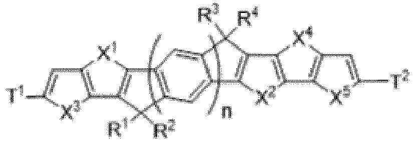
- the compound comprises the structure:
- solubilising groups can be placed anywhere on the structure, the inventors have found that the preferable positioning of solubilising groups at the "bridge head" positions on five membered rings adjacent the central ring or rings provides a greater solubilising effect than when positioned at the periphery of the molecule.
- shorter and/or smaller solubilising groups may be used at then bridge head position. These shorter and/or smaller solubilising groups are less able to interfere with ⁇ - ⁇ stacking, thereby potentially providing improved mobility in addition to improved solution processability.
- the improved solubility afforded by the positioning of the solubilising groups allows the planar conjugated structure of the semiconducting species to be further extended while the species remains soluble.
- Ar 2 is a homo-cyclic or heterocyclic aromatic ring. Where Ar 2 is a heterocyclic aromatic ring, it preferably comprises at least one heteroatom selected from the group S, O, NR 5 or SiR 6 R 7 .
- the compound comprises one or more further aromatic groups fused in series to Ar 1 and/or, if present, Ar 2 .
- One, some, or all of said further aromatic groups may be, and in some embodiments are, heterocyclic groups containing at least one heteroatom selected from the group S, O, NR 5 or SiR 6 R 7 .
- one or both of the terminal aryl or heteroaryl groups of the compound is substituted with one or more substituents T, at least one of which groups is a reactive or polymerisable group or optionally substituted straight, branched or cyclic alkyl chains having 1 to 20 ( e . g . 1 to 12) carbon atoms, alkoxy, amino, amido, silyl, alkyl, alkenyl, aryl or hetero aryl, the remaining groups, if any, independently comprising hydrogen or straight, branched or cyclic alkyl chains having 1 to 20 ( e . g . 1 to 12) carbon atoms, alkoxy, amino, amino, amido, silyl, alkyl, or alkenyl.
- substituents T at least one of which groups is a reactive or polymerisable group or optionally substituted straight, branched or cyclic alkyl chains having 1 to 20 ( e . g . 1 to 12) carbon atoms, alkoxy
- the reactive or polymerisable groups or groups T preferably are independently selected from halogens, boronic acids, diboronic acids, esters of boronic and diboronic acids, alkylene groups or stannyl groups.
- the terminal aryl groups represent aryl groups fused to just one other aryl or heteroaryl group, for example, groups Ar 1 and Ar 2 in structure II.
- the compound has a structure selected from the group:
- X 3 to X 6 independently are S, O, NR 5 or SiR 6 R 7 , and where R 5 to R 7 independently is a C 1 to C 5 branched, straight or cyclic alkyl chain.
- the invention provides an electronic device comprising a semiconducting portion comprising a compound described herein.
- the invention provides a solution for applying to the surface of a substrate to form a semiconducting portion on the substrate, the solution comprising a compound as described herein.
- the invention provides a method of manufacturing an electronic device comprising applying a solution as described herein onto a substrate.
- Organic semiconductors according to the present invention may be manufactured by means of a Suzuki-type cross-coupling reaction of a pinacol boronate of a thienothiophene with a diethyl-2,5-dibromoterephthalate in the presence of Pd(PPh 3 ) 4 and K 2 CO 3 to give a diketo compound. Further reaction with methyl lithium followed by a BF 3 ⁇ Et 2 O-mediated cyclization affords the compounds of the invention as shown in Figure 1 .
- the resulting compounds are easily soluble and may thus be applied by inkjet printing or other suitable solution deposition technique onto a substrate to provide the semiconducting layer 15 in a thin film transistor such as is shown in Figure 2 .
- An application of such an organic thin film transistor may be to drive pixels in an optical device, preferably an organic optical device.
- optical devices include photoresponsive devices, in particular photodetectors, and light-emissive devices, in particular organic light emitting devices.
- OTFTs are particularly suited for use with active matrix organic light emitting devices, e.g. for use in display applications.
- FIG. 3 shows a pixel comprising an organic thin film transistor 100 and an adjacent organic light emitting device (OLED) 102 fabricated on a common substrate 104.
- the OTFT 100 comprises gate electrode 106, dielectric layer 108, source and drain electrodes 110 and 112 respectively, and OSC layer 114.
- the OLED 102 comprises anode 116, cathode 118 and an electroluminescent layer 120 provided between the anode 116 and cathode 118. Further layers may be located between the anode 116 and cathode 118, such as charge transporting, charge injecting or charge blocking layers.
- the layer of cathode material 118 extends across both the OTFT 100 and the OLED 102, and an insulating layer 122 is provided to electrically isolate the cathode layer 118 from the OSC layer 122.
- the active areas of the OTFT 100 and the OLED 102 are defined by a common bank material formed by depositing a layer of photoresist 124 on substrate 104 and patterning it to define OTFT 100 and OLED 102 areas on the substrate.
- the drain electrode 112 is directly connected to the anode 116 of the organic light emitting device 102 for switching the organic light emitting device 102 between emitting and non-emitting states.
- an organic thin film transistor 200 may be fabricated in a stacked relationship to an organic light emitting device 202.
- the organic thin film transistor 202 is built up as described above in either a top or bottom gate configuration.
- the active areas of the OTFT 200 and OLED 202 are defined by a patterned layer of photoresist 124, however in this stacked arrangement, there are two separate bank layers 124 - one for the OLED 202 and one for the OTFT 200.
- a planarisation layer 204 (also known as a passivation layer) is deposited over the OTFT 200.
- Exemplary passivation layers 204 include BCBs and parylenes.
- the organic light emitting device 202 is fabricated over the passivation layer 204 and the anode 116 of the organic light emitting device 202 is electrically connected to the drain electrode 112 of the OTFT 200 by a conductive via 206 passing through passivation layer 204 and bank layer 124.
- pixel circuits comprising an OTFT and an optically active area (e.g. light emitting or light sensing area) may comprise further elements.
- the OLED pixel circuits of Figures 35 and 4 will typically comprise least one further transistor in addition to the driving transistor shown, and at least one capacitor.
- the organic light emitting devices described herein may be top or bottom emitting devices. That is, the devices may emit light through either the anode or cathode side of the device. In a transparent device, both the anode and cathode are transparent.
- a transparent cathode device need not have a transparent anode (unless, of course, a fully transparent device is desired), and so the transparent anode used for bottom-emitting devices may be replaced or supplemented with a layer of reflective material such as a layer of aluminium.
- Transparent cathodes are particularly advantageous for active matrix devices because emission through a transparent anode in such devices may be at least partially blocked by OTFT drive circuitry located underneath the emissive pixels as can be seen from the embodiment illustrated in Figure 4 .
- Thicknesses of the gate electrode, source and drain electrodes may be in the region of 5 - 200nm, although typically 50nm as measured by Atomic Force Microscopy (AFM), for example.
- AFM Atomic Force Microscopy
- a self assembled monolayer may be provided on the gate, source or drain electrodes, and/or one may be provided on the substrate, insulating layer and organic semiconductor material to promote crystallinity, reduce contact resistance, repair surface characteristics and promote adhesion where required.
- the dielectric surface in the channel region may be provided with a monolayer comprising a binding region and an organic region to improve device performance, e.g. by improving the organic semiconductor's morphology (in particular polymer alignment and crystallinity) and covering charge traps, in particular for a high k dielectric surface.
- Exemplary materials for such a monolayer include chloro- or alkoxysilanes with long alkyl chains, e . g . octadecyltrichlorosilane.
Landscapes
- Chemical & Material Sciences (AREA)
- Organic Chemistry (AREA)
- Physics & Mathematics (AREA)
- Spectroscopy & Molecular Physics (AREA)
- Engineering & Computer Science (AREA)
- Materials Engineering (AREA)
- Thin Film Transistor (AREA)
- Heterocyclic Carbon Compounds Containing A Hetero Ring Having Oxygen Or Sulfur (AREA)
- Electroluminescent Light Sources (AREA)
- Polyoxymethylene Polymers And Polymers With Carbon-To-Carbon Bonds (AREA)
- Metal-Oxide And Bipolar Metal-Oxide Semiconductor Integrated Circuits (AREA)
Claims (10)
- Halbleitende Verbindung, umfassend die folgende Struktur aufweist:
 R1 bis R4 unabhängig ausgewählt sind aus geraden, verzweigten oder zyklischen Alkylketten, die 2 bis 20 Kohlenstoffatome aufweisen; einer Alkoxygruppe; einer Aminogruppe; einer Amidogruppe; einer Silylgruppe; einer Alkylgruppe; einer Alkenylgruppe; einer Arylgruppe; oder einer Heteroarylgruppe;X1 und X2 unabhängig S oder O sind;Ar1 ein heterocyclischer aromatischer Ring ist;Ar2 ein homozyklischer oder heterozyklischer aromatischer Ring ist; undn eine ganze Zahl zwischen 1 und 4 ist;und wobei die halbleitende Verbindung eine oder mehrere weitere aromatische Gruppen umfasst, die in Reihe an Ar1 und/oder Ar2 kondensiert sind.
 - Halbleitende Verbindung nach Anspruch 1, wobei Ar2 ein heterocyclischer aromatischer Ring ist.
- Halbleitende Verbindung nach einem der vorherigen Ansprüche, wobei mindestens eine der weiteren aromatischen Gruppen eine heterocyclische Gruppe umfasst.
- Halbleitende Verbindung nach einem der vorherigen Ansprüche, wobei eine oder beide endständigen Arylgruppen der halbleitenden Verbindung mit einer oder mehreren Gruppen T substituiert sind, wobei mindestens eine der Gruppen T eine reaktive oder polymerisierbare Gruppe oder eine optional substituierte gerade, verzweigte oder zyklische Alkylkette, die 1 bis 20 Kohlenstoffatome aufweist; eine Alkoxygruppe; eine Aminogruppe; eine Amidogruppe; eine Silylgruppe; eine Alkylgruppe; eine Alkenylgruppe; eine Arylgruppe; oder eine Heteroarylgruppe ist, wobei die reaktive oder polymerisierbare Gruppe oder Gruppen T unabhängig ausgewählt sind aus Halogenen, Boronsäuren, Diboronsäuren, Estern von Boron- und Diboronsäuren, Alkylengruppen und Stannylgruppen.
- Halbleitende Verbindung nach Anspruch 4, wobei die halbleitende Verbindung eine Struktur aufweist, die ausgewählt ist aus der Gruppe:

X3 bis X6 unabhängig S, O, NR5 oder SiR6R7 sind und wobei R5 bis R7 unabhängig eine verzweigte, zyklische oder gerade C1- bis C5-Alkylkette sind und T1 und T2 Gruppen T sind, wie sie in Anspruch 4 definiert sind. - Halbleitende Verbindung nach einem der vorherigen Ansprüche, wobei mindestens eines von R1 bis R4 eine gerade, verzweigte oder cyclische Alkylkette ist, die 2 bis 12 Kohlenstoffatome aufweist.
- Halbleiterverbindung nach Anspruch 6, wobei mindestens eines von R1 bis R4 optional substituierte gerade, verzweigte oder zyklische Alkylketten umfasst, die 2 bis 6 Kohlenstoffatome aufweisen.
- Elektronische Vorrichtung, umfassend eine halbleitende Verbindung nach einem der vorherigen Ansprüche.
- Lösung zum Aufbringen auf eine Oberfläche eines Substrats, um einen halbleitenden Abschnitt auf dem Substrat zu bilden, die Lösung umfassend eine halbleitende Verbindung nach einem der Ansprüche 1-7.
- Verfahren zum Herstellen einer elektronischen Vorrichtung, umfassend ein Aufbringen einer Lösung nach Anspruch 9 auf ein Substrat.
Applications Claiming Priority (5)
| Application Number | Priority Date | Filing Date | Title |
|---|---|---|---|
| GB0913628.4A GB2472413B (en) | 2009-08-05 | 2009-08-05 | Organic semiconductors |
| EP18198795.9A EP3447057B1 (de) | 2009-08-05 | 2010-08-05 | Organische halbleiter |
| EP10852323A EP2462146A1 (de) | 2009-08-05 | 2010-08-05 | Organische halbleiter |
| PCT/GB2010/001485 WO2012017184A1 (en) | 2009-08-05 | 2010-08-05 | Organic semiconductors |
| EP16002060.8A EP3141551A1 (de) | 2009-08-05 | 2010-08-05 | Organische halbleiter |
Related Parent Applications (4)
| Application Number | Title | Priority Date | Filing Date |
|---|---|---|---|
| EP10852323A Division EP2462146A1 (de) | 2009-08-05 | 2010-08-05 | Organische halbleiter |
| EP18198795.9A Division-Into EP3447057B1 (de) | 2009-08-05 | 2010-08-05 | Organische halbleiter |
| EP18198795.9A Division EP3447057B1 (de) | 2009-08-05 | 2010-08-05 | Organische halbleiter |
| EP16002060.8A Division EP3141551A1 (de) | 2009-08-05 | 2010-08-05 | Organische halbleiter |
Publications (2)
| Publication Number | Publication Date |
|---|---|
| EP3524610A1 EP3524610A1 (de) | 2019-08-14 |
| EP3524610B1 true EP3524610B1 (de) | 2022-10-05 |
Family
ID=41129648
Family Applications (4)
| Application Number | Title | Priority Date | Filing Date |
|---|---|---|---|
| EP16002060.8A Ceased EP3141551A1 (de) | 2009-08-05 | 2010-08-05 | Organische halbleiter |
| EP10852323A Ceased EP2462146A1 (de) | 2009-08-05 | 2010-08-05 | Organische halbleiter |
| EP19164312.1A Active EP3524610B1 (de) | 2009-08-05 | 2010-08-05 | Organische halbleiter |
| EP18198795.9A Active EP3447057B1 (de) | 2009-08-05 | 2010-08-05 | Organische halbleiter |
Family Applications Before (2)
| Application Number | Title | Priority Date | Filing Date |
|---|---|---|---|
| EP16002060.8A Ceased EP3141551A1 (de) | 2009-08-05 | 2010-08-05 | Organische halbleiter |
| EP10852323A Ceased EP2462146A1 (de) | 2009-08-05 | 2010-08-05 | Organische halbleiter |
Family Applications After (1)
| Application Number | Title | Priority Date | Filing Date |
|---|---|---|---|
| EP18198795.9A Active EP3447057B1 (de) | 2009-08-05 | 2010-08-05 | Organische halbleiter |
Country Status (7)
| Country | Link |
|---|---|
| US (1) | US8853679B2 (de) |
| EP (4) | EP3141551A1 (de) |
| JP (2) | JP5812355B2 (de) |
| KR (1) | KR101787121B1 (de) |
| CN (1) | CN102482291A (de) |
| GB (1) | GB2472413B (de) |
| WO (1) | WO2012017184A1 (de) |
Families Citing this family (20)
| Publication number | Priority date | Publication date | Assignee | Title |
|---|---|---|---|---|
| JP6101263B2 (ja) * | 2011-07-19 | 2017-03-22 | メルク パテント ゲゼルシャフト ミット ベシュレンクテル ハフツングMerck Patent Gesellschaft mit beschraenkter Haftung | 有機半導体 |
| JP2015501303A (ja) * | 2011-10-20 | 2015-01-15 | メルク パテント ゲゼルシャフト ミット ベシュレンクテル ハフツングMerck Patent Gesellschaft mit beschraenkter Haftung | 有機半導体 |
| KR20140135749A (ko) | 2012-02-16 | 2014-11-26 | 메르크 파텐트 게엠베하 | 유기 반도체성 중합체 |
| KR102016198B1 (ko) | 2012-04-25 | 2019-08-29 | 메르크 파텐트 게엠베하 | 공액 중합체 |
| EP2904067A1 (de) * | 2012-10-05 | 2015-08-12 | Merck Patent GmbH | Organische halbleiter |
| US20150333263A1 (en) | 2012-12-07 | 2015-11-19 | Merck Patent Gmbh | Polymer comprising a naphthalene group and its use in organic electronic devices |
| WO2014094954A1 (en) * | 2012-12-18 | 2014-06-26 | Merck Patent Gmbh | Indenophenanthrene based compounds |
| KR102173046B1 (ko) * | 2013-12-06 | 2020-11-03 | 삼성디스플레이 주식회사 | 축합환 화합물 및 이를 포함한 유기 발광 소자 |
| JP6252264B2 (ja) * | 2014-03-12 | 2017-12-27 | 住友化学株式会社 | 高分子化合物およびそれを用いた有機半導体素子 |
| CN105315298B (zh) * | 2014-08-04 | 2017-10-10 | 中国科学院化学研究所 | 基于七并稠环单元的a‑d‑a共轭分子及其制备方法和应用 |
| CN104557972B (zh) * | 2015-01-20 | 2017-02-22 | 武汉理工大学 | 双(噻吩并[3,2‑b]噻吩)并芴单体、共轭聚合物及其应用 |
| JP6979699B2 (ja) | 2015-12-10 | 2021-12-15 | クラップ カンパニー リミテッドClap Co., Ltd. | ナフトインダセノジチオフェンおよびポリマー |
| CN106905344B (zh) * | 2015-12-23 | 2018-11-30 | 北京大学 | 基于七并稠环单元的共轭大分子及其制备方法和在太阳能电池中的应用 |
| EP3409722A1 (de) | 2016-01-29 | 2018-12-05 | Sumitomo Chemical Company Limited | Zusammensetzung und organischer dünnschichttransistor mit verwendung davon |
| CN108164547B (zh) * | 2016-12-07 | 2020-04-03 | 北京大学 | 多并稠环共轭大分子及其制备方法和应用 |
| EP3762979A1 (de) | 2018-03-07 | 2021-01-13 | Clap Co., Ltd. | Strukturierungsverfahren zur herstellung von organischen feldeffekttransistoren mit oberem tor und unterem kontakt |
| WO2020062254A1 (en) * | 2018-09-30 | 2020-04-02 | Southern University Of Science And Technology | Chlorine atoms induced molecular interlocked network in a non-fullerene acceptor |
| CN112912381B (zh) * | 2018-10-15 | 2023-09-05 | Clap有限公司 | 作为有机半导体的引达省衍生物 |
| WO2020085579A1 (ko) * | 2018-10-22 | 2020-04-30 | 경상대학교산학협력단 | 신규한 스피로 화합물 및 이를 이용하는 유기 전자 소자 |
| CN115109233B (zh) * | 2021-03-19 | 2023-05-23 | 华南理工大学 | 一种高效稳定聚合物空穴传输层材料和钙钛矿太阳电池器件及其制备方法 |
Citations (1)
| Publication number | Priority date | Publication date | Assignee | Title |
|---|---|---|---|---|
| WO2013010614A2 (en) * | 2011-07-19 | 2013-01-24 | Merck Patent Gmbh | Organic semiconductors |
Family Cites Families (14)
| Publication number | Priority date | Publication date | Assignee | Title |
|---|---|---|---|---|
| US5331183A (en) * | 1992-08-17 | 1994-07-19 | The Regents Of The University Of California | Conjugated polymer - acceptor heterojunctions; diodes, photodiodes, and photovoltaic cells |
| WO1997030445A1 (en) * | 1996-02-16 | 1997-08-21 | Philips Electronics N.V. | Write-once read-many electrical memory element of a conjugated polymer or oligomer |
| WO2000053656A1 (en) | 1999-03-05 | 2000-09-14 | Cambridge Display Technology Limited | Polymer preparation |
| JP4552023B2 (ja) * | 2003-11-07 | 2010-09-29 | 独立行政法人科学技術振興機構 | 多環縮環型π共役有機材料、その合成中間体、多環縮環型π共役有機材料の製造方法、および多環縮環型π共役有機材料の合成中間体の製造方法 |
| JP2007088222A (ja) | 2005-09-22 | 2007-04-05 | Konica Minolta Holdings Inc | 有機半導体材料、有機半導体膜、有機半導体デバイス及び有機薄膜トランジスタ |
| JP5007988B2 (ja) * | 2005-10-27 | 2012-08-22 | 国立大学法人名古屋大学 | 多環縮環化合物およびそれらの製造法ならびに多環縮環化合物を用いる有機電界発光素子 |
| EP1961052B1 (de) | 2005-12-12 | 2013-03-06 | Basf Se | Organische halbleiter und ihre herstellung |
| TWI345326B (en) | 2006-03-29 | 2011-07-11 | Pioneer Corp | Organic thin film transistor device and manufacturing method therefor |
| US7557370B2 (en) * | 2006-04-06 | 2009-07-07 | Xerox Corporation | Heteroacene polymers and electronic devices generated therefrom |
| JP4900670B2 (ja) * | 2006-05-01 | 2012-03-21 | Jnc株式会社 | 有機電界発光素子 |
| US8217387B2 (en) * | 2006-07-31 | 2012-07-10 | Sumitomo Chemical Company, Limited | Polymer compound and light emitting device using the same |
| CN101939325A (zh) * | 2008-02-06 | 2011-01-05 | 住友化学株式会社 | 有机半导体材料 |
| US8637857B2 (en) * | 2010-04-06 | 2014-01-28 | Basf Se | Substituted carbazole derivatives and use thereof in organic electronics |
| WO2012050001A1 (ja) * | 2010-10-12 | 2012-04-19 | 新日鐵化学株式会社 | 含カルコゲン芳香族化合物、有機半導体材料及び有機電子デバイス |
-
2009
- 2009-08-05 GB GB0913628.4A patent/GB2472413B/en active Active
-
2010
- 2010-08-05 EP EP16002060.8A patent/EP3141551A1/de not_active Ceased
- 2010-08-05 KR KR1020127005640A patent/KR101787121B1/ko active Active
- 2010-08-05 WO PCT/GB2010/001485 patent/WO2012017184A1/en not_active Ceased
- 2010-08-05 EP EP10852323A patent/EP2462146A1/de not_active Ceased
- 2010-08-05 JP JP2012527375A patent/JP5812355B2/ja active Active
- 2010-08-05 EP EP19164312.1A patent/EP3524610B1/de active Active
- 2010-08-05 CN CN2010800394499A patent/CN102482291A/zh active Pending
- 2010-08-05 EP EP18198795.9A patent/EP3447057B1/de active Active
- 2010-08-05 US US13/387,020 patent/US8853679B2/en active Active
-
2015
- 2015-07-09 JP JP2015138071A patent/JP6053880B2/ja active Active
Patent Citations (1)
| Publication number | Priority date | Publication date | Assignee | Title |
|---|---|---|---|---|
| WO2013010614A2 (en) * | 2011-07-19 | 2013-01-24 | Merck Patent Gmbh | Organic semiconductors |
Non-Patent Citations (1)
| Title |
|---|
| DAI SHUIXING ET AL: "Effect of Core Size on Performance of Fused-Ring Electron Acceptors", CHEMISTRY OF MATERIALS, vol. 30, no. 15, 2 July 2018 (2018-07-02), US, pages 5390 - 5396, XP055818947, ISSN: 0897-4756, DOI: 10.1021/acs.chemmater.8b02222 * |
Also Published As
| Publication number | Publication date |
|---|---|
| JP2013501076A (ja) | 2013-01-10 |
| US8853679B2 (en) | 2014-10-07 |
| EP2462146A1 (de) | 2012-06-13 |
| EP3141551A1 (de) | 2017-03-15 |
| CN102482291A (zh) | 2012-05-30 |
| GB0913628D0 (en) | 2009-09-16 |
| EP3447057A1 (de) | 2019-02-27 |
| EP3447057B1 (de) | 2021-10-06 |
| US20120184089A1 (en) | 2012-07-19 |
| KR101787121B1 (ko) | 2017-10-18 |
| JP5812355B2 (ja) | 2015-11-11 |
| JP6053880B2 (ja) | 2016-12-27 |
| GB2472413B (en) | 2014-04-23 |
| WO2012017184A1 (en) | 2012-02-09 |
| KR20120069675A (ko) | 2012-06-28 |
| EP3524610A1 (de) | 2019-08-14 |
| JP2015227461A (ja) | 2015-12-17 |
| GB2472413A (en) | 2011-02-09 |
Similar Documents
| Publication | Publication Date | Title |
|---|---|---|
| EP3524610B1 (de) | Organische halbleiter | |
| KR101788329B1 (ko) | 유기 반도체 | |
| US9187493B2 (en) | Heterocyclic compound and use thereof | |
| US20150303383A1 (en) | Novel Condensed Polycyclic Aromatic Compound And Use Thereof | |
| TWI614254B (zh) | 新穎之縮合多環芳香族化合物及其用途 | |
| US8946448B2 (en) | Organic semiconductors | |
| US8680138B2 (en) | Organic semiconductors | |
| HK1169407A (en) | Organic semiconductors |
Legal Events
| Date | Code | Title | Description |
|---|---|---|---|
| PUAI | Public reference made under article 153(3) epc to a published international application that has entered the european phase |
Free format text: ORIGINAL CODE: 0009012 |
|
| STAA | Information on the status of an ep patent application or granted ep patent |
Free format text: STATUS: THE APPLICATION HAS BEEN PUBLISHED |
|
| AC | Divisional application: reference to earlier application |
Ref document number: 3141551 Country of ref document: EP Kind code of ref document: P Ref document number: 2462146 Country of ref document: EP Kind code of ref document: P Ref document number: 3447057 Country of ref document: EP Kind code of ref document: P |
|
| AK | Designated contracting states |
Kind code of ref document: A1 Designated state(s): AL AT BE BG CH CY CZ DE DK EE ES FI FR GB GR HR HU IE IS IT LI LT LU LV MC MK MT NL NO PL PT RO SE SI SK SM TR |
|
| STAA | Information on the status of an ep patent application or granted ep patent |
Free format text: STATUS: REQUEST FOR EXAMINATION WAS MADE |
|
| 17P | Request for examination filed |
Effective date: 20200214 |
|
| RBV | Designated contracting states (corrected) |
Designated state(s): AL AT BE BG CH CY CZ DE DK EE ES FI FR GB GR HR HU IE IS IT LI LT LU LV MC MK MT NL NO PL PT RO SE SI SK SM TR |
|
| STAA | Information on the status of an ep patent application or granted ep patent |
Free format text: STATUS: EXAMINATION IS IN PROGRESS |
|
| 17Q | First examination report despatched |
Effective date: 20200924 |
|
| GRAP | Despatch of communication of intention to grant a patent |
Free format text: ORIGINAL CODE: EPIDOSNIGR1 |
|
| STAA | Information on the status of an ep patent application or granted ep patent |
Free format text: STATUS: GRANT OF PATENT IS INTENDED |
|
| INTG | Intention to grant announced |
Effective date: 20220513 |
|
| GRAS | Grant fee paid |
Free format text: ORIGINAL CODE: EPIDOSNIGR3 |
|
| GRAA | (expected) grant |
Free format text: ORIGINAL CODE: 0009210 |
|
| STAA | Information on the status of an ep patent application or granted ep patent |
Free format text: STATUS: THE PATENT HAS BEEN GRANTED |
|
| AC | Divisional application: reference to earlier application |
Ref document number: 2462146 Country of ref document: EP Kind code of ref document: P Ref document number: 3141551 Country of ref document: EP Kind code of ref document: P Ref document number: 3447057 Country of ref document: EP Kind code of ref document: P |
|
| AK | Designated contracting states |
Kind code of ref document: B1 Designated state(s): AL AT BE BG CH CY CZ DE DK EE ES FI FR GB GR HR HU IE IS IT LI LT LU LV MC MK MT NL NO PL PT RO SE SI SK SM TR |
|
| REG | Reference to a national code |
Ref country code: GB Ref legal event code: FG4D |
|
| REG | Reference to a national code |
Ref country code: CH Ref legal event code: EP |
|
| REG | Reference to a national code |
Ref country code: AT Ref legal event code: REF Ref document number: 1522692 Country of ref document: AT Kind code of ref document: T Effective date: 20221015 |
|
| REG | Reference to a national code |
Ref country code: DE Ref legal event code: R096 Ref document number: 602010068515 Country of ref document: DE |
|
| REG | Reference to a national code |
Ref country code: IE Ref legal event code: FG4D |
|
| REG | Reference to a national code |
Ref country code: LT Ref legal event code: MG9D |
|
| REG | Reference to a national code |
Ref country code: NL Ref legal event code: MP Effective date: 20221005 |
|
| REG | Reference to a national code |
Ref country code: AT Ref legal event code: MK05 Ref document number: 1522692 Country of ref document: AT Kind code of ref document: T Effective date: 20221005 |
|
| PG25 | Lapsed in a contracting state [announced via postgrant information from national office to epo] |
Ref country code: NL Free format text: LAPSE BECAUSE OF FAILURE TO SUBMIT A TRANSLATION OF THE DESCRIPTION OR TO PAY THE FEE WITHIN THE PRESCRIBED TIME-LIMIT Effective date: 20221005 |
|
| PG25 | Lapsed in a contracting state [announced via postgrant information from national office to epo] |
Ref country code: SE Free format text: LAPSE BECAUSE OF FAILURE TO SUBMIT A TRANSLATION OF THE DESCRIPTION OR TO PAY THE FEE WITHIN THE PRESCRIBED TIME-LIMIT Effective date: 20221005 Ref country code: PT Free format text: LAPSE BECAUSE OF FAILURE TO SUBMIT A TRANSLATION OF THE DESCRIPTION OR TO PAY THE FEE WITHIN THE PRESCRIBED TIME-LIMIT Effective date: 20230206 Ref country code: NO Free format text: LAPSE BECAUSE OF FAILURE TO SUBMIT A TRANSLATION OF THE DESCRIPTION OR TO PAY THE FEE WITHIN THE PRESCRIBED TIME-LIMIT Effective date: 20230105 Ref country code: LT Free format text: LAPSE BECAUSE OF FAILURE TO SUBMIT A TRANSLATION OF THE DESCRIPTION OR TO PAY THE FEE WITHIN THE PRESCRIBED TIME-LIMIT Effective date: 20221005 Ref country code: FI Free format text: LAPSE BECAUSE OF FAILURE TO SUBMIT A TRANSLATION OF THE DESCRIPTION OR TO PAY THE FEE WITHIN THE PRESCRIBED TIME-LIMIT Effective date: 20221005 Ref country code: ES Free format text: LAPSE BECAUSE OF FAILURE TO SUBMIT A TRANSLATION OF THE DESCRIPTION OR TO PAY THE FEE WITHIN THE PRESCRIBED TIME-LIMIT Effective date: 20221005 Ref country code: AT Free format text: LAPSE BECAUSE OF FAILURE TO SUBMIT A TRANSLATION OF THE DESCRIPTION OR TO PAY THE FEE WITHIN THE PRESCRIBED TIME-LIMIT Effective date: 20221005 |
|
| PG25 | Lapsed in a contracting state [announced via postgrant information from national office to epo] |
Ref country code: PL Free format text: LAPSE BECAUSE OF FAILURE TO SUBMIT A TRANSLATION OF THE DESCRIPTION OR TO PAY THE FEE WITHIN THE PRESCRIBED TIME-LIMIT Effective date: 20221005 Ref country code: LV Free format text: LAPSE BECAUSE OF FAILURE TO SUBMIT A TRANSLATION OF THE DESCRIPTION OR TO PAY THE FEE WITHIN THE PRESCRIBED TIME-LIMIT Effective date: 20221005 Ref country code: IS Free format text: LAPSE BECAUSE OF FAILURE TO SUBMIT A TRANSLATION OF THE DESCRIPTION OR TO PAY THE FEE WITHIN THE PRESCRIBED TIME-LIMIT Effective date: 20230205 Ref country code: HR Free format text: LAPSE BECAUSE OF FAILURE TO SUBMIT A TRANSLATION OF THE DESCRIPTION OR TO PAY THE FEE WITHIN THE PRESCRIBED TIME-LIMIT Effective date: 20221005 Ref country code: GR Free format text: LAPSE BECAUSE OF FAILURE TO SUBMIT A TRANSLATION OF THE DESCRIPTION OR TO PAY THE FEE WITHIN THE PRESCRIBED TIME-LIMIT Effective date: 20230106 |
|
| REG | Reference to a national code |
Ref country code: DE Ref legal event code: R097 Ref document number: 602010068515 Country of ref document: DE |
|
| P01 | Opt-out of the competence of the unified patent court (upc) registered |
Effective date: 20230527 |
|
| PG25 | Lapsed in a contracting state [announced via postgrant information from national office to epo] |
Ref country code: SM Free format text: LAPSE BECAUSE OF FAILURE TO SUBMIT A TRANSLATION OF THE DESCRIPTION OR TO PAY THE FEE WITHIN THE PRESCRIBED TIME-LIMIT Effective date: 20221005 Ref country code: RO Free format text: LAPSE BECAUSE OF FAILURE TO SUBMIT A TRANSLATION OF THE DESCRIPTION OR TO PAY THE FEE WITHIN THE PRESCRIBED TIME-LIMIT Effective date: 20221005 Ref country code: EE Free format text: LAPSE BECAUSE OF FAILURE TO SUBMIT A TRANSLATION OF THE DESCRIPTION OR TO PAY THE FEE WITHIN THE PRESCRIBED TIME-LIMIT Effective date: 20221005 Ref country code: DK Free format text: LAPSE BECAUSE OF FAILURE TO SUBMIT A TRANSLATION OF THE DESCRIPTION OR TO PAY THE FEE WITHIN THE PRESCRIBED TIME-LIMIT Effective date: 20221005 Ref country code: CZ Free format text: LAPSE BECAUSE OF FAILURE TO SUBMIT A TRANSLATION OF THE DESCRIPTION OR TO PAY THE FEE WITHIN THE PRESCRIBED TIME-LIMIT Effective date: 20221005 |
|
| PLBE | No opposition filed within time limit |
Free format text: ORIGINAL CODE: 0009261 |
|
| STAA | Information on the status of an ep patent application or granted ep patent |
Free format text: STATUS: NO OPPOSITION FILED WITHIN TIME LIMIT |
|
| PG25 | Lapsed in a contracting state [announced via postgrant information from national office to epo] |
Ref country code: SK Free format text: LAPSE BECAUSE OF FAILURE TO SUBMIT A TRANSLATION OF THE DESCRIPTION OR TO PAY THE FEE WITHIN THE PRESCRIBED TIME-LIMIT Effective date: 20221005 Ref country code: AL Free format text: LAPSE BECAUSE OF FAILURE TO SUBMIT A TRANSLATION OF THE DESCRIPTION OR TO PAY THE FEE WITHIN THE PRESCRIBED TIME-LIMIT Effective date: 20221005 |
|
| 26N | No opposition filed |
Effective date: 20230706 |
|
| PG25 | Lapsed in a contracting state [announced via postgrant information from national office to epo] |
Ref country code: SI Free format text: LAPSE BECAUSE OF FAILURE TO SUBMIT A TRANSLATION OF THE DESCRIPTION OR TO PAY THE FEE WITHIN THE PRESCRIBED TIME-LIMIT Effective date: 20221005 |
|
| PG25 | Lapsed in a contracting state [announced via postgrant information from national office to epo] |
Ref country code: MC Free format text: LAPSE BECAUSE OF FAILURE TO SUBMIT A TRANSLATION OF THE DESCRIPTION OR TO PAY THE FEE WITHIN THE PRESCRIBED TIME-LIMIT Effective date: 20221005 |
|
| REG | Reference to a national code |
Ref country code: CH Ref legal event code: PL |
|
| PG25 | Lapsed in a contracting state [announced via postgrant information from national office to epo] |
Ref country code: MC Free format text: LAPSE BECAUSE OF FAILURE TO SUBMIT A TRANSLATION OF THE DESCRIPTION OR TO PAY THE FEE WITHIN THE PRESCRIBED TIME-LIMIT Effective date: 20221005 |
|
| PG25 | Lapsed in a contracting state [announced via postgrant information from national office to epo] |
Ref country code: LU Free format text: LAPSE BECAUSE OF NON-PAYMENT OF DUE FEES Effective date: 20230805 |
|
| GBPC | Gb: european patent ceased through non-payment of renewal fee |
Effective date: 20230805 |
|
| PG25 | Lapsed in a contracting state [announced via postgrant information from national office to epo] |
Ref country code: LU Free format text: LAPSE BECAUSE OF NON-PAYMENT OF DUE FEES Effective date: 20230805 Ref country code: CH Free format text: LAPSE BECAUSE OF NON-PAYMENT OF DUE FEES Effective date: 20230831 |
|
| REG | Reference to a national code |
Ref country code: BE Ref legal event code: MM Effective date: 20230831 |
|
| REG | Reference to a national code |
Ref country code: IE Ref legal event code: MM4A |
|
| PG25 | Lapsed in a contracting state [announced via postgrant information from national office to epo] |
Ref country code: IT Free format text: LAPSE BECAUSE OF FAILURE TO SUBMIT A TRANSLATION OF THE DESCRIPTION OR TO PAY THE FEE WITHIN THE PRESCRIBED TIME-LIMIT Effective date: 20221005 |
|
| PG25 | Lapsed in a contracting state [announced via postgrant information from national office to epo] |
Ref country code: IE Free format text: LAPSE BECAUSE OF NON-PAYMENT OF DUE FEES Effective date: 20230805 |
|
| PG25 | Lapsed in a contracting state [announced via postgrant information from national office to epo] |
Ref country code: GB Free format text: LAPSE BECAUSE OF NON-PAYMENT OF DUE FEES Effective date: 20230805 |
|
| PG25 | Lapsed in a contracting state [announced via postgrant information from national office to epo] |
Ref country code: IE Free format text: LAPSE BECAUSE OF NON-PAYMENT OF DUE FEES Effective date: 20230805 Ref country code: GB Free format text: LAPSE BECAUSE OF NON-PAYMENT OF DUE FEES Effective date: 20230805 |
|
| PG25 | Lapsed in a contracting state [announced via postgrant information from national office to epo] |
Ref country code: BE Free format text: LAPSE BECAUSE OF NON-PAYMENT OF DUE FEES Effective date: 20230831 |
|
| PGFP | Annual fee paid to national office [announced via postgrant information from national office to epo] |
Ref country code: DE Payment date: 20240828 Year of fee payment: 15 |
|
| PGFP | Annual fee paid to national office [announced via postgrant information from national office to epo] |
Ref country code: FR Payment date: 20240826 Year of fee payment: 15 |
|
| PG25 | Lapsed in a contracting state [announced via postgrant information from national office to epo] |
Ref country code: BG Free format text: LAPSE BECAUSE OF FAILURE TO SUBMIT A TRANSLATION OF THE DESCRIPTION OR TO PAY THE FEE WITHIN THE PRESCRIBED TIME-LIMIT Effective date: 20221005 |
|
| PG25 | Lapsed in a contracting state [announced via postgrant information from national office to epo] |
Ref country code: BG Free format text: LAPSE BECAUSE OF FAILURE TO SUBMIT A TRANSLATION OF THE DESCRIPTION OR TO PAY THE FEE WITHIN THE PRESCRIBED TIME-LIMIT Effective date: 20221005 |
|
| PG25 | Lapsed in a contracting state [announced via postgrant information from national office to epo] |
Ref country code: CY Free format text: LAPSE BECAUSE OF FAILURE TO SUBMIT A TRANSLATION OF THE DESCRIPTION OR TO PAY THE FEE WITHIN THE PRESCRIBED TIME-LIMIT; INVALID AB INITIO Effective date: 20100805 |
|
| PG25 | Lapsed in a contracting state [announced via postgrant information from national office to epo] |
Ref country code: HU Free format text: LAPSE BECAUSE OF FAILURE TO SUBMIT A TRANSLATION OF THE DESCRIPTION OR TO PAY THE FEE WITHIN THE PRESCRIBED TIME-LIMIT; INVALID AB INITIO Effective date: 20100805 |
|
| PG25 | Lapsed in a contracting state [announced via postgrant information from national office to epo] |
Ref country code: TR Free format text: LAPSE BECAUSE OF FAILURE TO SUBMIT A TRANSLATION OF THE DESCRIPTION OR TO PAY THE FEE WITHIN THE PRESCRIBED TIME-LIMIT Effective date: 20221005 |
|
| REG | Reference to a national code |
Ref country code: DE Ref legal event code: R119 Ref document number: 602010068515 Country of ref document: DE |