EP3524660B1 - Organische lichtemittierende vorrichtung mit langer lebensdauer, niedriger spannung und hohem wirkungsgrad - Google Patents
Organische lichtemittierende vorrichtung mit langer lebensdauer, niedriger spannung und hohem wirkungsgrad Download PDFInfo
- Publication number
- EP3524660B1 EP3524660B1 EP17858625.1A EP17858625A EP3524660B1 EP 3524660 B1 EP3524660 B1 EP 3524660B1 EP 17858625 A EP17858625 A EP 17858625A EP 3524660 B1 EP3524660 B1 EP 3524660B1
- Authority
- EP
- European Patent Office
- Prior art keywords
- carbon atoms
- substituted
- unsubstituted
- chemical formula
- organic light
- Prior art date
- Legal status (The legal status is an assumption and is not a legal conclusion. Google has not performed a legal analysis and makes no representation as to the accuracy of the status listed.)
- Active
Links
Images

Classifications
-
- H—ELECTRICITY
- H10—SEMICONDUCTOR DEVICES; ELECTRIC SOLID-STATE DEVICES NOT OTHERWISE PROVIDED FOR
- H10K—ORGANIC ELECTRIC SOLID-STATE DEVICES
- H10K85/00—Organic materials used in the body or electrodes of devices covered by this subclass
- H10K85/60—Organic compounds having low molecular weight
- H10K85/649—Aromatic compounds comprising a hetero atom
- H10K85/657—Polycyclic condensed heteroaromatic hydrocarbons
- H10K85/6574—Polycyclic condensed heteroaromatic hydrocarbons comprising only oxygen in the heteroaromatic polycondensed ring system, e.g. cumarine dyes
-
- C—CHEMISTRY; METALLURGY
- C09—DYES; PAINTS; POLISHES; NATURAL RESINS; ADHESIVES; COMPOSITIONS NOT OTHERWISE PROVIDED FOR; APPLICATIONS OF MATERIALS NOT OTHERWISE PROVIDED FOR
- C09K—MATERIALS FOR MISCELLANEOUS APPLICATIONS, NOT PROVIDED FOR ELSEWHERE
- C09K11/00—Luminescent materials, e.g. electroluminescent or chemiluminescent
- C09K11/06—Luminescent materials, e.g. electroluminescent or chemiluminescent containing organic luminescent materials
-
- H—ELECTRICITY
- H10—SEMICONDUCTOR DEVICES; ELECTRIC SOLID-STATE DEVICES NOT OTHERWISE PROVIDED FOR
- H10K—ORGANIC ELECTRIC SOLID-STATE DEVICES
- H10K50/00—Organic light-emitting devices
- H10K50/10—OLEDs or polymer light-emitting diodes [PLED]
- H10K50/11—OLEDs or polymer light-emitting diodes [PLED] characterised by the electroluminescent [EL] layers
-
- H—ELECTRICITY
- H10—SEMICONDUCTOR DEVICES; ELECTRIC SOLID-STATE DEVICES NOT OTHERWISE PROVIDED FOR
- H10K—ORGANIC ELECTRIC SOLID-STATE DEVICES
- H10K50/00—Organic light-emitting devices
- H10K50/10—OLEDs or polymer light-emitting diodes [PLED]
- H10K50/14—Carrier transporting layers
- H10K50/15—Hole transporting layers
-
- H—ELECTRICITY
- H10—SEMICONDUCTOR DEVICES; ELECTRIC SOLID-STATE DEVICES NOT OTHERWISE PROVIDED FOR
- H10K—ORGANIC ELECTRIC SOLID-STATE DEVICES
- H10K50/00—Organic light-emitting devices
- H10K50/10—OLEDs or polymer light-emitting diodes [PLED]
- H10K50/14—Carrier transporting layers
- H10K50/16—Electron transporting layers
-
- H—ELECTRICITY
- H10—SEMICONDUCTOR DEVICES; ELECTRIC SOLID-STATE DEVICES NOT OTHERWISE PROVIDED FOR
- H10K—ORGANIC ELECTRIC SOLID-STATE DEVICES
- H10K50/00—Organic light-emitting devices
- H10K50/10—OLEDs or polymer light-emitting diodes [PLED]
- H10K50/17—Carrier injection layers
-
- H—ELECTRICITY
- H10—SEMICONDUCTOR DEVICES; ELECTRIC SOLID-STATE DEVICES NOT OTHERWISE PROVIDED FOR
- H10K—ORGANIC ELECTRIC SOLID-STATE DEVICES
- H10K50/00—Organic light-emitting devices
- H10K50/10—OLEDs or polymer light-emitting diodes [PLED]
- H10K50/17—Carrier injection layers
- H10K50/171—Electron injection layers
-
- H—ELECTRICITY
- H10—SEMICONDUCTOR DEVICES; ELECTRIC SOLID-STATE DEVICES NOT OTHERWISE PROVIDED FOR
- H10K—ORGANIC ELECTRIC SOLID-STATE DEVICES
- H10K71/00—Manufacture or treatment specially adapted for the organic devices covered by this subclass
- H10K71/10—Deposition of organic active material
-
- H—ELECTRICITY
- H10—SEMICONDUCTOR DEVICES; ELECTRIC SOLID-STATE DEVICES NOT OTHERWISE PROVIDED FOR
- H10K—ORGANIC ELECTRIC SOLID-STATE DEVICES
- H10K85/00—Organic materials used in the body or electrodes of devices covered by this subclass
- H10K85/40—Organosilicon compounds, e.g. TIPS pentacene
-
- H—ELECTRICITY
- H10—SEMICONDUCTOR DEVICES; ELECTRIC SOLID-STATE DEVICES NOT OTHERWISE PROVIDED FOR
- H10K—ORGANIC ELECTRIC SOLID-STATE DEVICES
- H10K85/00—Organic materials used in the body or electrodes of devices covered by this subclass
- H10K85/60—Organic compounds having low molecular weight
- H10K85/615—Polycyclic condensed aromatic hydrocarbons, e.g. anthracene
-
- H—ELECTRICITY
- H10—SEMICONDUCTOR DEVICES; ELECTRIC SOLID-STATE DEVICES NOT OTHERWISE PROVIDED FOR
- H10K—ORGANIC ELECTRIC SOLID-STATE DEVICES
- H10K85/00—Organic materials used in the body or electrodes of devices covered by this subclass
- H10K85/60—Organic compounds having low molecular weight
- H10K85/631—Amine compounds having at least two aryl rest on at least one amine-nitrogen atom, e.g. triphenylamine
- H10K85/636—Amine compounds having at least two aryl rest on at least one amine-nitrogen atom, e.g. triphenylamine comprising heteroaromatic hydrocarbons as substituents on the nitrogen atom
-
- H—ELECTRICITY
- H10—SEMICONDUCTOR DEVICES; ELECTRIC SOLID-STATE DEVICES NOT OTHERWISE PROVIDED FOR
- H10K—ORGANIC ELECTRIC SOLID-STATE DEVICES
- H10K85/00—Organic materials used in the body or electrodes of devices covered by this subclass
- H10K85/60—Organic compounds having low molecular weight
- H10K85/649—Aromatic compounds comprising a hetero atom
- H10K85/657—Polycyclic condensed heteroaromatic hydrocarbons
- H10K85/6572—Polycyclic condensed heteroaromatic hydrocarbons comprising only nitrogen in the heteroaromatic polycondensed ring system, e.g. phenanthroline or carbazole
-
- H—ELECTRICITY
- H10—SEMICONDUCTOR DEVICES; ELECTRIC SOLID-STATE DEVICES NOT OTHERWISE PROVIDED FOR
- H10K—ORGANIC ELECTRIC SOLID-STATE DEVICES
- H10K85/00—Organic materials used in the body or electrodes of devices covered by this subclass
- H10K85/60—Organic compounds having low molecular weight
- H10K85/649—Aromatic compounds comprising a hetero atom
- H10K85/657—Polycyclic condensed heteroaromatic hydrocarbons
- H10K85/6576—Polycyclic condensed heteroaromatic hydrocarbons comprising only sulfur in the heteroaromatic polycondensed ring system, e.g. benzothiophene
-
- C—CHEMISTRY; METALLURGY
- C09—DYES; PAINTS; POLISHES; NATURAL RESINS; ADHESIVES; COMPOSITIONS NOT OTHERWISE PROVIDED FOR; APPLICATIONS OF MATERIALS NOT OTHERWISE PROVIDED FOR
- C09K—MATERIALS FOR MISCELLANEOUS APPLICATIONS, NOT PROVIDED FOR ELSEWHERE
- C09K2211/00—Chemical nature of organic luminescent or tenebrescent compounds
- C09K2211/10—Non-macromolecular compounds
- C09K2211/1003—Carbocyclic compounds
- C09K2211/1011—Condensed systems
-
- C—CHEMISTRY; METALLURGY
- C09—DYES; PAINTS; POLISHES; NATURAL RESINS; ADHESIVES; COMPOSITIONS NOT OTHERWISE PROVIDED FOR; APPLICATIONS OF MATERIALS NOT OTHERWISE PROVIDED FOR
- C09K—MATERIALS FOR MISCELLANEOUS APPLICATIONS, NOT PROVIDED FOR ELSEWHERE
- C09K2211/00—Chemical nature of organic luminescent or tenebrescent compounds
- C09K2211/10—Non-macromolecular compounds
- C09K2211/1003—Carbocyclic compounds
- C09K2211/1014—Carbocyclic compounds bridged by heteroatoms, e.g. N, P, Si or B
-
- C—CHEMISTRY; METALLURGY
- C09—DYES; PAINTS; POLISHES; NATURAL RESINS; ADHESIVES; COMPOSITIONS NOT OTHERWISE PROVIDED FOR; APPLICATIONS OF MATERIALS NOT OTHERWISE PROVIDED FOR
- C09K—MATERIALS FOR MISCELLANEOUS APPLICATIONS, NOT PROVIDED FOR ELSEWHERE
- C09K2211/00—Chemical nature of organic luminescent or tenebrescent compounds
- C09K2211/10—Non-macromolecular compounds
- C09K2211/1018—Heterocyclic compounds
- C09K2211/1025—Heterocyclic compounds characterised by ligands
- C09K2211/1029—Heterocyclic compounds characterised by ligands containing one nitrogen atom as the heteroatom
-
- C—CHEMISTRY; METALLURGY
- C09—DYES; PAINTS; POLISHES; NATURAL RESINS; ADHESIVES; COMPOSITIONS NOT OTHERWISE PROVIDED FOR; APPLICATIONS OF MATERIALS NOT OTHERWISE PROVIDED FOR
- C09K—MATERIALS FOR MISCELLANEOUS APPLICATIONS, NOT PROVIDED FOR ELSEWHERE
- C09K2211/00—Chemical nature of organic luminescent or tenebrescent compounds
- C09K2211/10—Non-macromolecular compounds
- C09K2211/1018—Heterocyclic compounds
- C09K2211/1025—Heterocyclic compounds characterised by ligands
- C09K2211/1029—Heterocyclic compounds characterised by ligands containing one nitrogen atom as the heteroatom
- C09K2211/1033—Heterocyclic compounds characterised by ligands containing one nitrogen atom as the heteroatom with oxygen
-
- C—CHEMISTRY; METALLURGY
- C09—DYES; PAINTS; POLISHES; NATURAL RESINS; ADHESIVES; COMPOSITIONS NOT OTHERWISE PROVIDED FOR; APPLICATIONS OF MATERIALS NOT OTHERWISE PROVIDED FOR
- C09K—MATERIALS FOR MISCELLANEOUS APPLICATIONS, NOT PROVIDED FOR ELSEWHERE
- C09K2211/00—Chemical nature of organic luminescent or tenebrescent compounds
- C09K2211/10—Non-macromolecular compounds
- C09K2211/1018—Heterocyclic compounds
- C09K2211/1025—Heterocyclic compounds characterised by ligands
- C09K2211/1029—Heterocyclic compounds characterised by ligands containing one nitrogen atom as the heteroatom
- C09K2211/1037—Heterocyclic compounds characterised by ligands containing one nitrogen atom as the heteroatom with sulfur
-
- C—CHEMISTRY; METALLURGY
- C09—DYES; PAINTS; POLISHES; NATURAL RESINS; ADHESIVES; COMPOSITIONS NOT OTHERWISE PROVIDED FOR; APPLICATIONS OF MATERIALS NOT OTHERWISE PROVIDED FOR
- C09K—MATERIALS FOR MISCELLANEOUS APPLICATIONS, NOT PROVIDED FOR ELSEWHERE
- C09K2211/00—Chemical nature of organic luminescent or tenebrescent compounds
- C09K2211/10—Non-macromolecular compounds
- C09K2211/1018—Heterocyclic compounds
- C09K2211/1025—Heterocyclic compounds characterised by ligands
- C09K2211/1088—Heterocyclic compounds characterised by ligands containing oxygen as the only heteroatom
Definitions
- the present disclosure relates to an organic light-emitting diode with long lifespan, low driving voltage, and high efficiency and, more particularly, to an organic light-emitting diode wherein host and dopant materials of specific structures are used in a light-emitting layer to ensure long lifespan, low voltage, and high efficiency.
- OLEDs Organic light-emitting diodes
- OLEDs based on self-luminescence, are used to create digital displays with the advantage of having a wide viewing angle and being able to be made thinner and lighter than liquid crystal displays.
- an OLED display exhibits a very fast response time. Accordingly, OLEDs find applications in the full color display field or the illumination field.
- Materials used as the organic layers in organic light emitting diodes may be divided into luminescent materials and charge charrier materials on the basis of functions, for example, a hole injection materials, a hole transport material, an electron injection material, and an electron transport material.
- the light emitting mechanisms allow the luminescent materials to be classified as fluorescent and phosphorescent materials, which use excitons in singlet and triplet states, respectively.
- a host-dopant system may be used as a luminescent material so as to increase the color purity and the light emitting efficiency through energy transfer.
- Korean Patent No. 10-2008-0015865 A (February 20, 2008 ), which describes an organic light emitting device using an arylamine-coupled indenofluorene derivative
- Korean patent No. 10-2012-0047706 A (May 14, 2012 ) which describes an organic light emitting device using a compound having dibenzofuran or dibenzothiophene that coexists with fluorescence or carbazole within a single molecule.
- Korean Patent No. 10-2015-0043020 A (April 22, 2015 ), which discloses an organic light-emitting diode employing an anthracene derivative as a fluorescent host
- organic light-emitting diodes including a light-emitting layer material that shows a longer lifespan, a lower voltage, and higher efficiency.
- US 2015/333277 A1 discloses the compound represented by BH1 as a host and a compound represented by Formula I as a dopant in an OLED.
- KR 2012 0135501 A discloses compound 178 falling under the general formula of anthracene compounds represented by Chemical Formula C.
- the purpose of the present disclosure is to provide a novel organic light-emitting diode with a long lifespan, a low driving voltage, and high efficiency, wherein dopant and host materials of specific structures are introduced into a light-emitting layer.
- the present disclosure provides an organic light-emitting diode according to claim 1 and the use thereof according to claim 11. Preferred embodiments are set forth in the subclaims.
- the organic light-emitting diode according to the present disclosure has longer lifespan, lower driving voltage and improved efficiency, compared to conventional organic light-emitting diodes.
- FIG. 1 is a schematic view of an organic light-emitting diode according to an embodiment of the present disclosure.
- the organic light-emitting diode may further comprise at least one of a hole injection layer, a hole transport layer, a functional layer capable of both hole injection and hole transport, an electron transport layer, and an electron injection layer in addition to the light-emitting layer.
- the first electrode is an anode and the second electrode is a cathode
- a hole transport layer and a hole injection layer are disposed between the anode and the light-emitting layer
- an electron transport layer and an electron injection layer are sequentially arranged between the light-emitting layer and the cathode.
- the light-emitting layer may include at least one of the amine compounds represented by the following [Chemical Formula A] and at least one of the anthracene compounds represented by the following [Chemical Formula B] or [Chemical Formula C].
- an organic layer includes at least one organic compound
- (an organic layer) may be construed to mean that "(an organic layer) may include a single organic compound species or two or more difference species of organic compounds falling within the scope of the present disclosure.
- the light-emitting layer includes a host and a dopant, wherein compounds other than the anthracene compounds and amine compounds according to the present disclosure may be additional used.
- the content of the dopant may range from about 0.01 to 20 parts by weight, based on 100 parts by weight of the host, but is not limited thereto.
- an electron donating molecule having a low ionization potential is suitable.
- diamine, triamine, or tetraamine derivatives having a triphenylamine skeleton are employed, as exemplified by N,N'-bis(3-methylphenyl)-N,N'-dipehenyl-[1,1-bisphenyl]-4,4'-diamine or N,N'-di(naphthalen-1-yl)-N,N'-diphenylbenzidine (a-NPD).
- a hole injection layer may be further deposited beneath the hole transport layer.
- HIL hole injection layer
- No particular limitations are imparted to the hole injection layer material, as long as it is one that is typically used in the art. Examples include HATCN (hexaazatriphenylenehexacarbonitrile), CuPc(copperphthalocyanine), the starburst amines TCTA (4,4',4"-tri(N-carbazolyl)triphenyl-amine), and m-MTDATA (4,4',4"-tris-(3-methylphenylphenyl amino)triphenylamine), etc.
- the electron transport material functions to stably transport electrons injected from the electron injection electrode (cathode) and may be a material well known in the art.
- the well-known material include quinoline derivatives, particularly tris(8-quinolinolate)aluminum (Alq3), Liq, TAZ, BAlq, beryllium bis(benzoquinolin-10-oate) (Bebq2), Compound 201, Compound 202, BCP, and the oxadiazole derivatives PBD, BMD, and BND, but are not limited thereto.
- organic metal compound represented by Chemical Formula F may be used, either alone or in combination with the aforementioned material, as a compound for an electron transport layer in the present disclosure: [Chemical Formula F] Y m -M-(OA) n wherein,
- Y's which are the same or different, are each independently selected from the following Structural Formulas C1 to C39, but are not limited thereto: wherein, R's, which are the same or different, are each independently selected from among a hydrogen atom, a deuterium atom, a halogen, a cyano, a substituted or unsubstituted alkyl of 1 to 30 carbon atoms, a substituted or unsubstituted aryl of 6 to 30 carbon atoms, a substituted or unsubstituted heteroalkyl of 3 to 30 carbon atoms, a substituted or unsubstituted alkoxy of 1 to 30 carbon atoms, a substituted or unsubstituted cycloalkyl of 3 to 30 carbon atoms, a substituted or unsubstituted alkenyl of 2 to 30 carbon atoms, a substituted or unsubstituted alkylamino of 1 to 30 carbon atom
- substituted in the expression “substituted or unsubstituted” means having at least one substituent selected from the group consisting of a deuterium atom, a cyano, a halogen, a hydroxy, a nitro, an alkyl, an alkoxy, an alkylamino, an arylamino, a heteroarylamino, an alkylsilyl, an arylsilyl, an aryloxy, an aryl, a heteroaryl, a germanium, a phosphorus, and a boron.
- An electron injection layer that functions to facilitate electron injection from the cathode, thus improving the power efficiency of the diode, may be further deposited on the electron transport layer. So long as it is conventionally used in the art, any material can be available for the electron injection layer without particular limitations. Examples include LiF, NaCl, CsF, Li 2 O, and BaO.
- the electron injection layer may range in thickness from about 1 ⁇ to about 100 ⁇ and particularly from about 3 ⁇ to about 90 ⁇ . Given the thickness range for the electron injection layer, the diode can exhibit satisfactory electron injection properties without actually elevating a driving voltage.
- the cathode may be made of a metal or metal alloy such as lithium (Li), magnesium (Mg), aluminum (Al), aluminum-lithium (Al-Li), calcium (Ca), magnesium-indium (Mg-In), and magnesium-silver (Mg-Ag).
- a metal or metal alloy such as lithium (Li), magnesium (Mg), aluminum (Al), aluminum-lithium (Al-Li), calcium (Ca), magnesium-indium (Mg-In), and magnesium-silver (Mg-Ag).
- ITO or IZO may be employed to form a transparent cathode for a top-emitting organic light-emitting diode.
- one or more layers selected from among a hole injection layer, a hole transport layer, a functional layer capable of both hole injection and hole transport, a light-emitting layer, an electron transport layer, and an electron injection layer may be deposited using a deposition process or a solution process.
- the deposition process refers to a process by which a material is vaporized by heating in a vacuum or at a low pressure and deposited to form a thin film
- the solution process means a method in which a material for forming a layer is dissolved in a solvent and applied for the formation of a thin film by means of inkjet printing, roll-to-roll coating, screen printing, spray coating, dip coating, spin coating, etc.
- the organic light-emitting diode of the present disclosure may be applied to a device selected from among flat display devices; flexible display devices; monochrome or white flat illumination devices; and monochrome or white flexible illumination devices.
- the organic light-emitting diode of the present disclosure is explained below with reference to FIG. 1 .
- FIG. 1 is a schematic cross-sectional view of the structure of an organic light-emitting diode according to some embodiments of the present disclosure.
- the organic light-emitting diode comprises an anode 20, a hole transport layer 40, an organic light-emitting layer 50, an electron transport layer 60, and a cathode 80, and optionally a hole injection layer 30 and an electron injection layer 70.
- one or two intermediate layers may be further formed in the organic light-emitting diode, or a hole barrier layer or an electron barrier layer may also be employed.
- a substrate 10 is coated with an anode electrode material to form an anode 20.
- an anode electrode material is an organic substrate or transparent plastic substrate that exhibits excellent transparency, surface smoothness, ease of handling, and waterproofness.
- the anode electrode material indium tin oxide (ITO), indium zinc oxide (IZO), tin oxide (SnO 2 ), or zinc oxide (ZnO), which are transparent and superior in terms of conductivity, may be used.
- a hole injection layer material is applied on the anode electrode 20 by thermal deposition in a vacuum or by spin coating to form a hole injection layer 30. Subsequently, vacuum thermal deposition or spin coating may also be conducted to form a hole transport layer 40 with a hole transport layer material on the hole injection layer 30.
- an organic light-emitting layer 50 is deposited on the hole transport layer 40, optionally by followed by the formation of a hole barrier layer (not shown) on the organic light-emitting layer 50 by deposition in a vacuum or by spin coating.
- a hole barrier layer (not shown) on the organic light-emitting layer 50 by deposition in a vacuum or by spin coating.
- the hole barrier layer serves to prevent the introduction of holes into the cathode. Any material that has a higher ionization potential than the light-emitting compound may be used for the hole barrier layer without limitation. Representative among hole barrier materials are BAlq, BCP, TPBI.
- an electron transport layer 60 may be deposited on the hole barrier layer and may then be overlaid with an electron injection layer 70.
- a cathode metal is deposited on the electron injection layer 70 by thermal deposition in a vacuum to form a cathode 80, thus obtaining an organic EL diode.
- the cathode may be made of lithium (Li), magnesium (Mg), aluminum (Al), aluminum-lithium (Al-Li), calcium (Ca), magnesium-indium (Mg-In), or magnesium-silver (Mg-Ag).
- a transparent cathode made of ITO or IZO may be employed.
- Penta-deutero-chlorobenzene (11.7 g, 0.1 mol), 9-acridone (19.5 g, 0.1 mol), palladium acetate (0.08 g, 0.32 mmol), 2,2'-bis(diphenylphosphino)-1-1'-binaphthyl (0.26 g, 0.42 mmol), and sodium-tert-butoxide (15.2 g, 0.16 mol) were added to toluene (200 mL) and stirred for 12 hours under reflux. Subsequent to cooling to room temperature, washing with methanol and recrystallization in dichloromethane and methanol afforded [Intermediate 8-a] (20.7 g, yield 75%).
- An ITO glass substrate was patterned to have a translucent area of 2 mm ⁇ 2 mm and then rinsed.
- the substrate was mounted in a vacuum chamber, which was then set to have a base pressure of 1 ⁇ 10 -6 torr.
- films were formed of HATCN(50 ⁇ ) and NPD(650 ⁇ ) in the order.
- a light-emitting layer (200 ⁇ ) was formed of a mixture including the compounds shown in Table 1 as a host and a dopant (weight ratio 97:3) .
- [Chemical Formula E-1] and Liq was sequentially deposited to form an electron transport layer (300 ⁇ ) and an electron injection layer (10 ⁇ ), respectively, followed by formation of an Al layer (1,000 ⁇ ) to fabricate an organic light-emitting diode.
- the organic light-emitting diodes thus obtained were measured at 10 mA/cm 2 to determine the luminescence properties thereof.
- An organic light-emitting diode was fabricated in the same manner as in Examples 1 to 8, with the exception of using [BD1] as a dopant in the light-emitting layer.
- the organic light-emitting diode was measured at 10 mA/cm 2 to determine the luminescence properties thereof.
- the structure of [BD1] is as follows:
- An organic light-emitting diode was fabricated in the same manner as in Examples 1 to 8, with the exception of using [BH1] as a host in the light-emitting layer.
- the organic light-emitting diode was measured at 10 mA/cm 2 to determine the luminescence properties thereof.
- the structure of [BH1] is as follows:
- T97 refers to the time taken for the initial luminance to decrease to 97 % thereof.
- TABLE 1 Example Host Dopant V EQE T97 C. Ex. 1 Compound 3 BD1 4.2 8.0 52 C. Ex. 2 Compound 56 BD1 4.3 8.4 55 C. Ex. 3 BH1 Chemical Formula 3 4.2 7.9 44 C. Ex. 4 BH1 Chemical Formula 22 4.2 7.7 48 Ex. 1 Compound 3 Chemical Formula 3 3.7 9.7 115 Ex. 2 Compound 7 Chemical Formula 4 3.8 9. 6 118 Ex. 3 Compound 56 Chemical Formula 21 3.7 10.0 120 Ex. 4 Compound 115 Chemical Formula 22 3.7 9.8 125 Ex. 5 Compound 151 Chemical Formula 36 3.7 10.2 121 Ex. 6 Compound 155 Chemical Formula 40 3.8 9.5 115 Ex. 7 Compound 56 Chemical Formula 51 3.8 9.8 108 Ex. 8 Compound 151 Chemical Formula 64 3.7 9.8 110
- the OLEDs according to Examples 1 to 8 of the present disclosure could exhibit longer lifespan and operate at lower voltage with high efficiency than conventional OLEDs of Comparative Examples 1 to 4, thereby demonstrating their high applicability to organic electroluminescence devices.
- the organic light-emitting diode according to the present disclosure exhibits long lifespan, low voltage, and high efficiency properties and thus is industrially applicable.
Landscapes
- Chemical & Material Sciences (AREA)
- Physics & Mathematics (AREA)
- Engineering & Computer Science (AREA)
- Materials Engineering (AREA)
- Spectroscopy & Molecular Physics (AREA)
- Optics & Photonics (AREA)
- Organic Chemistry (AREA)
- Manufacturing & Machinery (AREA)
- Electroluminescent Light Sources (AREA)
Claims (11)
- Organische Leuchtdiode, umfassend: eine erste Elektrode; eine zweite Elektrode gegenüber der ersten Elektrode; und eine Licht abstrahlende Schicht, eingefügt zwischen der ersten Elektrode und der zweiten Elektrode,wobei die Licht abstrahlende Schicht mindestens eine der durch die folgende chemische Formel A dargestellten Aminverbindungen und mindestens eine der durch die folgende chemische Formel B oder C dargestellten Anthrazenverbindungen umfasst:
 X eines ist, gewählt unter NR11, O, S und SiR12R13,Z1 und Z2, die gleich oder verschieden sind, jeweils unabhängig ein beliebiges sind, gewählt unter einem substituierten oder unsubstituierten aromatischer Kohlenwasserstoffring von 6 bis 30 Kohlenstoffatomen, wobei zwei benachbarte Kohlenstoffatome von Z1 und zwei benachbarte Kohlenstoffatome von Z2 einen Fünfring bilden, womit ein kondensierter Ring etabliert ist,die Substituenten R1 bis R8 und R11 bis R13, die gleich oder verschieden sind, jeweils unabhängig eines sind, gewählt unter einem Wasserstoffatom, einem Deuteriumatom, einem substituierten oder unsubstituierten Alkyl von 1 bis 30 Kohlenstoffatomen, einem substituierten oder unsubstituierten Aryl von 6 bis 50 Kohlenstoffatomen, einem substituierten oder unsubstituierten Cycloalkyl von 3 bis 30 Kohlenstoffatomen, einem substituierten oder unsubstituierten Heteroaryl von 2 bis 50 Kohlenstoffatomen, tragend mindestens eines, gewählt unter O, N und S, als ein Heteroatom, einem substituierten oder unsubstituierten Alkylsilyl von 1 bis 30 Kohlenstoffatomen, einem substituierten oder unsubstituierten Arylsilyl von 6 bis 30 Kohlenstoffatomen, einem Cyano, einem Nitro und einem Halogen,angrenzende Substituenten von R1 bis R8 miteinander verbunden sein können, um einen mono- oder einen polyzyklischen aliphatischen oder aromatischen Ring zu bilden, der ein heterozyklischer Ring sein kann, tragend ein Heteroatom, gewählt unter N, S und O, als einen Ringbestandteil,A1 und A2, die gleich oder verschieden sind, jeweils unabhängig die folgende Strukturformel Q darstellen,
 * eine Bindestelle darstellt, an der ein Kohlenstoffatom von Z1 oder Z2, das nicht am Bilden des Fünfrings beteiligt ist, an A1 oder A2 gebunden ist,der Linker L eine Einzelbindung oder ein substituiertes oder unsubstituiertes Arylen von 6 bis 60 Kohlenstoffatomen darstellt;n eine ganze Zahl von 0 bis 2 ist, wobei, wenn n 2 ist, die Linker L gleich oder verschieden sind,die Substituenten Ar1 und Ar2, die gleich oder verschieden sind, jeweils unabhängig eines sind, gewählt unter einem substituierten oder unsubstituierten Aryl von 6 bis 40 Kohlenstoffatomen und einem substituierten oder unsubstituierten Heteroaryl von 2 bis 30 Kohlenstoffatomen;


R21 bis R28 und R31 bis R37, die gleich oder verschieden sind, jeweils unabhängig eines sind, gewählt unter einem Wasserstoffatom, einem Deuteriumatom, einem substituierten oder unsubstituierten Alkyl von 1 bis 30 Kohlenstoffatomen, einem substituierten oder unsubstituierten Cycloalkyl von 3 bis 30 Kohlenstoffatomen, einem substituierten oder unsubstituierten Aryl von 6 bis 50 Kohlenstoffatomen, einem substituierten oder unsubstituierten Heteroaryl von 2 bis 50 Kohlenstoffatomen, tragend O, N oder S als ein Heteroatom, einem Cyano, einem Nitro, einem Halogen, einem substituierten oder unsubstituierten Silyl von 1 bis 30 Kohlenstoffatomen, undder Substituent Ar3 eines ist, gewählt unter einem substituierten oder unsubstituierten Aryl von 6 bis 50 Kohlenstoffatomen und einem substituierten oder unsubstituierten Heteroaryl von 2 bis 50 Kohlenstoffatomen,wobei die durch die chemische Formel C dargestellte Anthrazenverbindung die folgende Verbindung H-B nicht enthält, wobei der Begriff "substituiert" in dem Ausdruck "substituiert oder unsubstituiert" bedeutet, dass mindestens ein Substituent vorliegt, gewählt unter der Gruppe, bestehend aus einem Deuterium, einem Cyano, einem Halogen, einem Nitro, einem Alkyl von 1 bis 24 Kohlenstoffatomen, einem halogenierten Alkyl von 1 bis 24 Kohlenstoffatomen, einem Aryl von 6 bis 24 Kohlenstoffatomen, einem Arylalkyl von 7 bis 24 Kohlenstoffatomen, einem Heteroaryl von 2 bis 24 Kohlenstoffatomen, einem Heteroarylalkyl von 2 bis 24 Kohlenstoffatomen, einem Alkylsilyl von 1 bis 24 Kohlenstoffatomen, einem Arylsilyl von 6 bis 24 Kohlenstoffatomen, und einem Aryloxy von 6 bis 24 Kohlenstoffatomen.
 - Organische Leuchtdiode nach Anspruch 1, wobei die Licht abstrahlende Schicht ein Grundmaterial und einen Dotierstoff umfasst, wobei die durch die chemische Formel B oder die chemische Formel C dargestellte Anthrazenverbindung als das Grundmaterial verwendet ist und die durch die chemische Formel A dargestellte Aminverbindung als der Dotierstoff verwendet ist.
- Organische Leuchtdiode nach Anspruch 1, wobei die Substituenten Ar3 in der chemischen Formel B und der chemischen Formel C jeweils substituiertes oder unsubstituiertes Aryl von 6 bis 18 Kohlenstoffatomen sind.
- Organische Leuchtdiode nach Anspruch 1, wobei Z1 und Z2 in der chemischen Formel A gleich oder verschieden sind und jeweils unabhängig ein substituierter oder unsubstituierter aromatischer Kohlenwasserstoffring von 6 bis 30 Kohlenstoffatomen sind.
- Organische Leuchtdiode nach Anspruch 1, wobei der Linker L in der chemischen Formel A eine einzelne Bindung oder eine unter den folgenden Strukturformeln 1, 2, 4, 6, 7 und 9 gewählte ist:


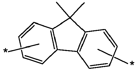
- Organische Leuchtdiode nach Anspruch 4, wobei der substituierte oder unsubstituierte aromatische Kohlenwasserstoffring von 6 bis 30 Kohlenstoffatomen einer ist, gewählt unter den folgenden Strukturformel 10 bis Strukturformel 21:




 "-*" eine Bindestelle zum Bilden des Fünfrings Z1 oder Z2 bezeichnet,R wie oben für R1 bis R8 definiert sind, undm eine Ganzzahl von 1 bis 8 ist, wobei, wenn m 2 oder größer ist, oder wenn zwei oder mehr R existieren, die einzelnen R gleich oder verschieden sind.
 - Organische Leuchtdiode nach Anspruch 3, wobei die Substituenten Ar3 in der chemischen Formel B und der chemischen Formel C jeweils ein Substituent sind, der durch die folgende Strukturformel C dargestellt ist:
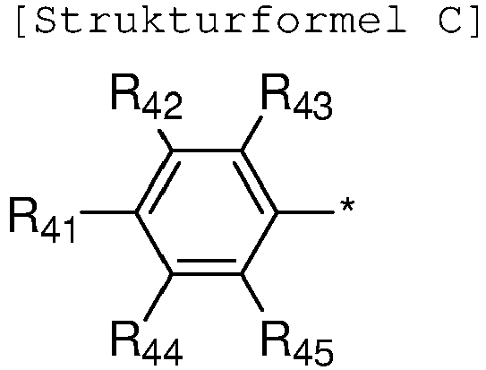
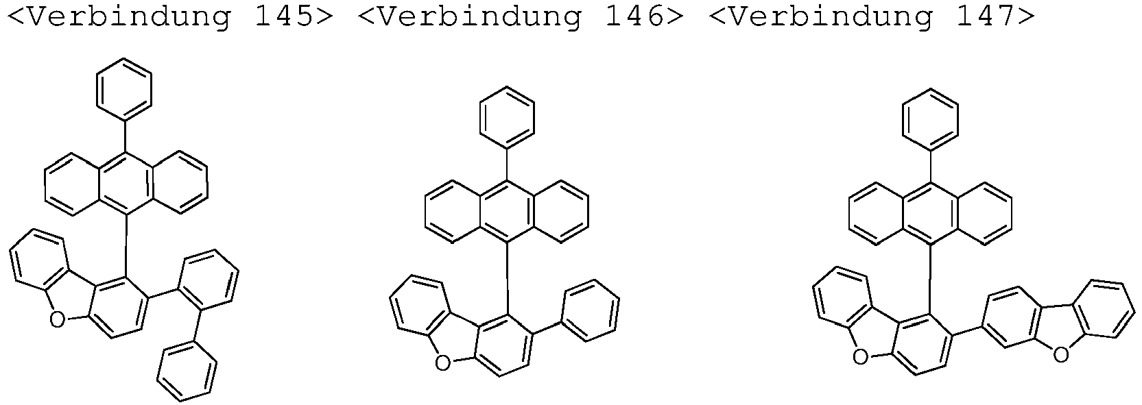
- Organische Leuchtdiode nach Anspruch 1, wobei die durch die chemische Formel B oder C dargestellte Anthrazenverbindung eine ist, gewählt unter den folgenden [Verbindung 1] bis [Verbindung 180]:
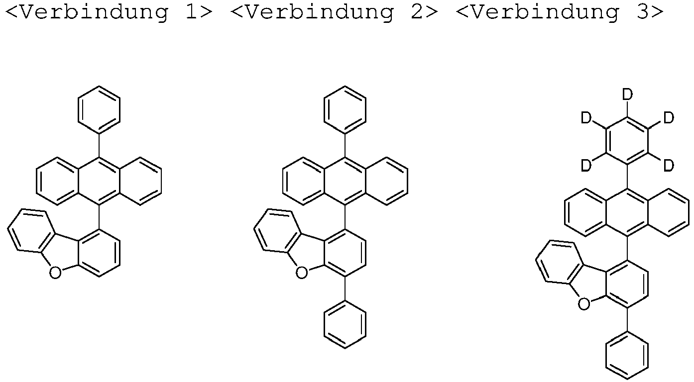


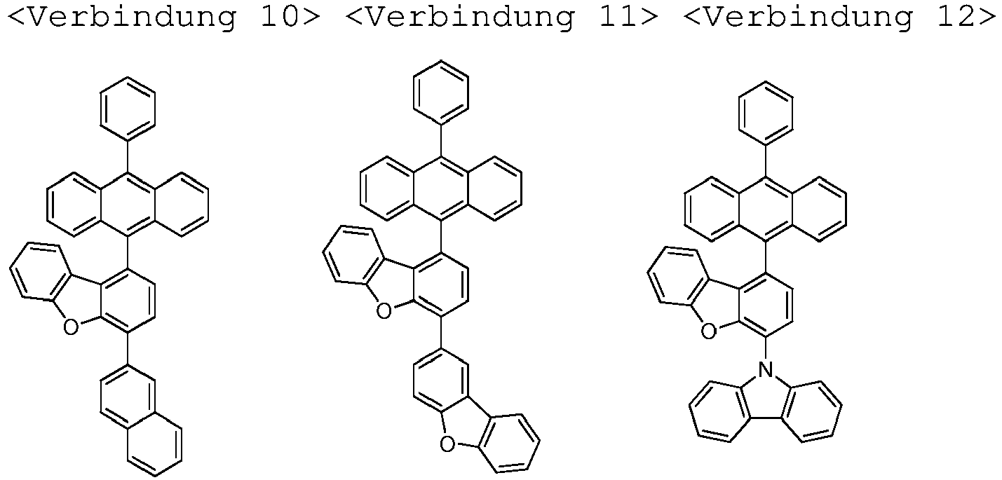


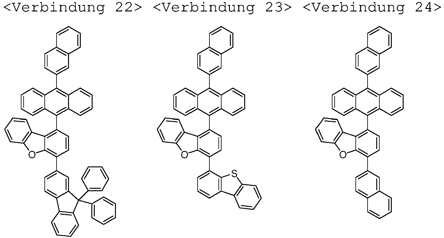

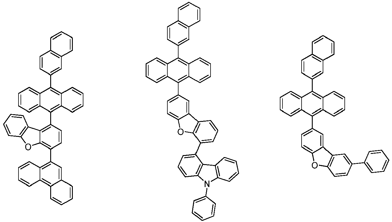


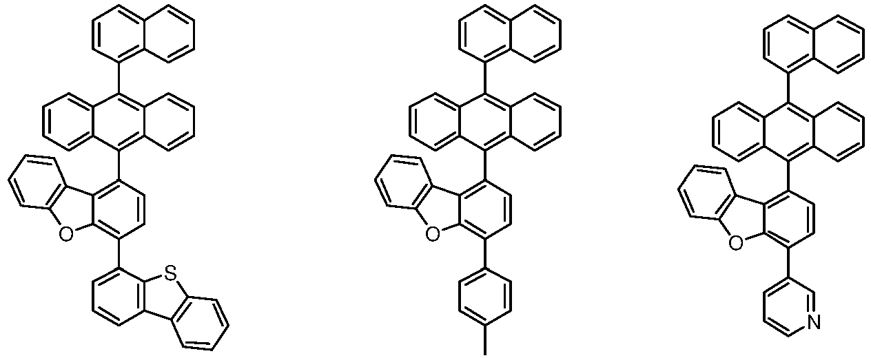




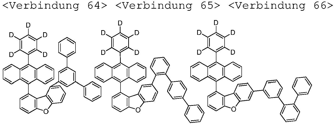





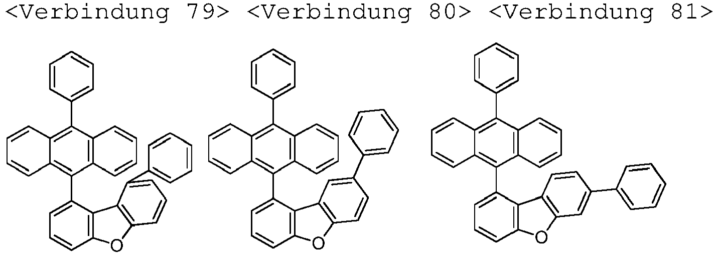
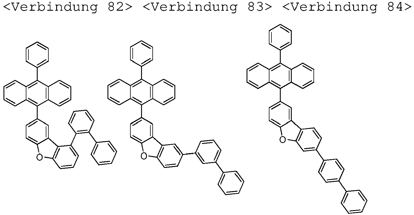


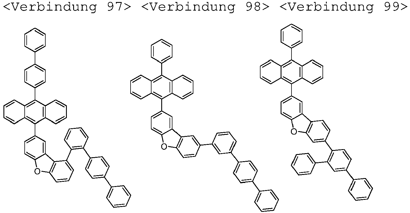


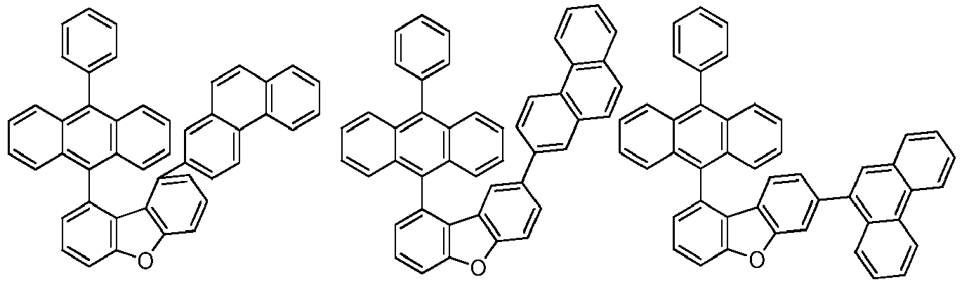


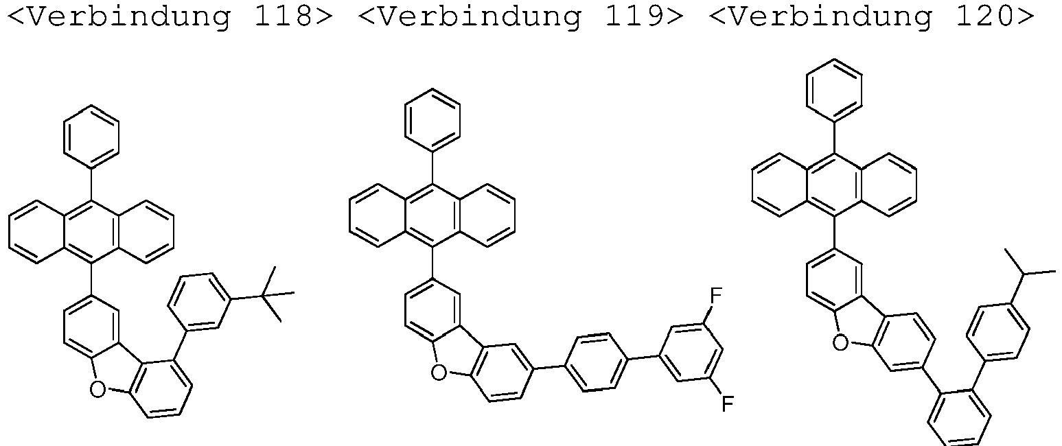


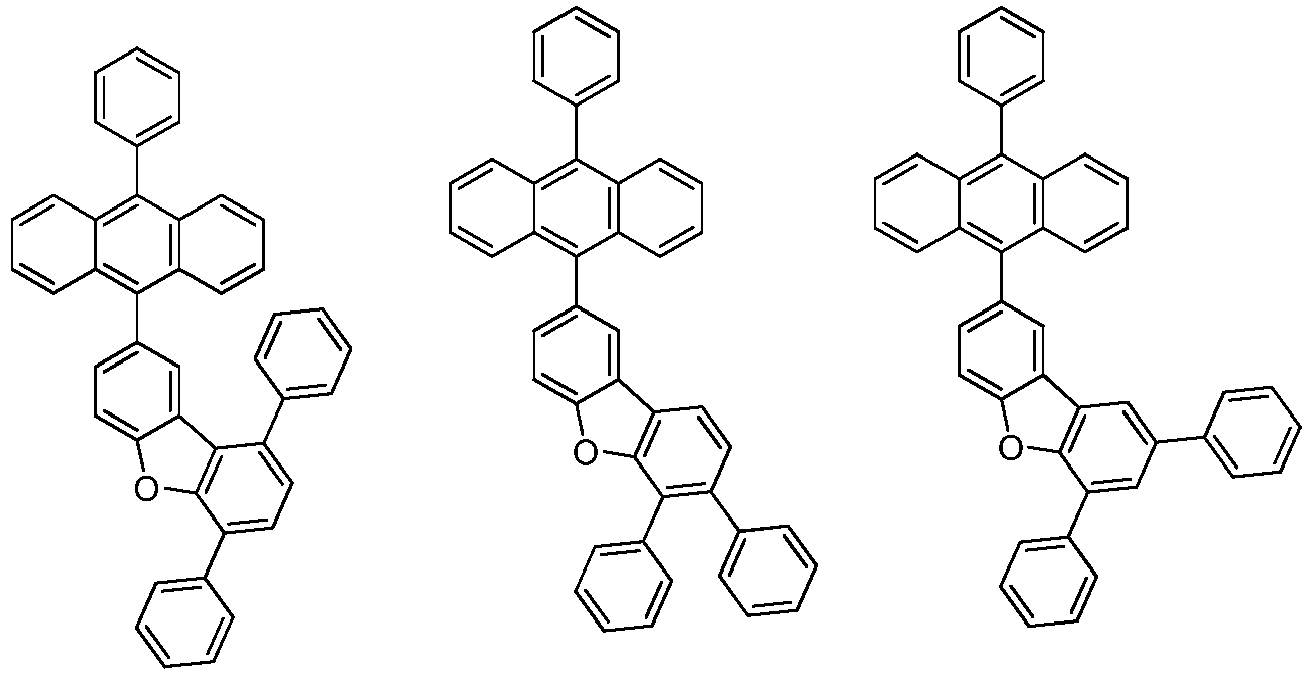
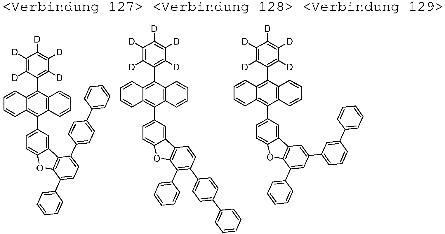


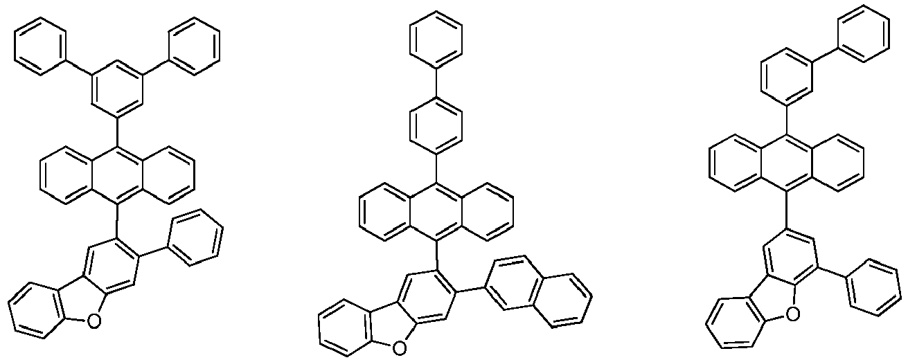











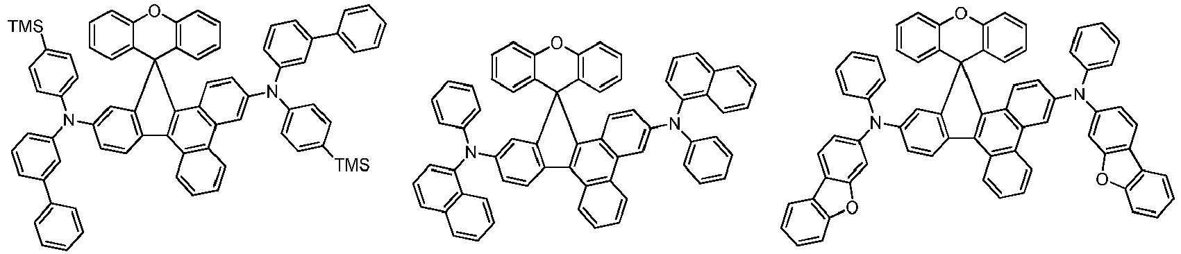
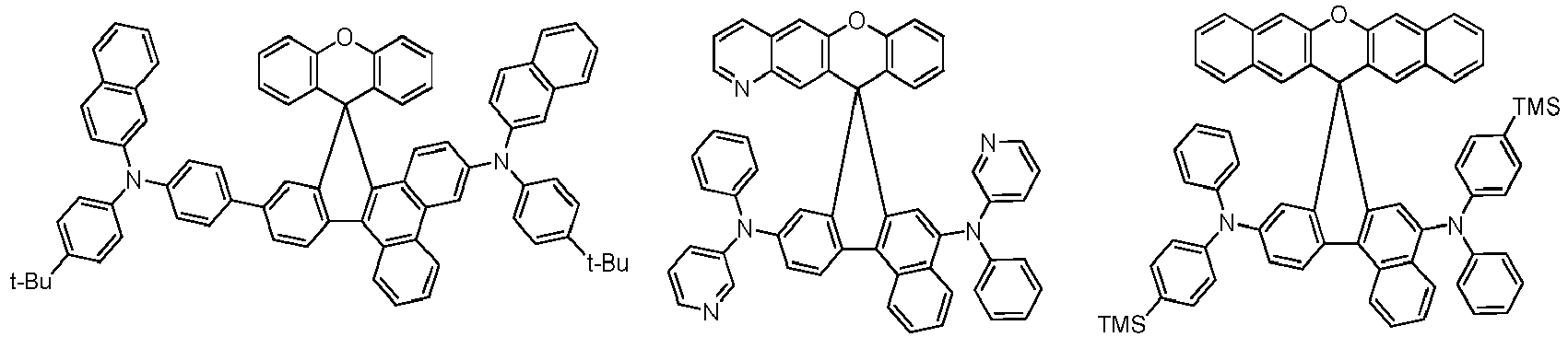
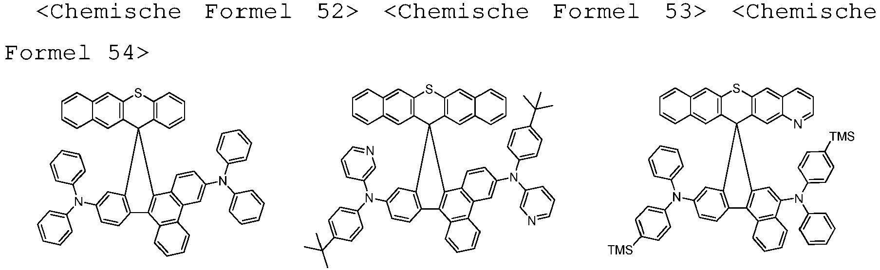
- Organische Leuchtdiode nach Anspruch 1, wobei die durch die chemische Formel A dargestellte Aminverbindung eine ist, gewählt unter den folgenden chemischen Formeln 1 bis 66:
<Chemische Formel 1> <Chemische Formel 2> <Chemische Formel 3>








- Organische Leuchtdiode nach Anspruch 1, weiter umfassend mindestens eine aus einer Loch-Injektionsschicht, einer Loch-Transportschicht, einer funktionellen Schicht, die in der Lage ist sowohl zur Loch-Injektion als auch zum Loch-Transport, einer Elektronentransportschicht und einer Elektroneninjektionsschicht, zusätzlich zur Licht abstrahlenden Schicht.
- Verwendung der organischen Leuchtdiode nach Anspruch 1 in einer Vorrichtung, gewählt unter einer Flachbildschirmvorrichtung, einer flexiblen Bildschirmvorrichtung, einer flachen monochromen oder Grauskala-Beleuchtungsvorrichtung und einer flexiblen monochromen oder Grauskala-Beleuchtungsvorrichtung.
Applications Claiming Priority (2)
| Application Number | Priority Date | Filing Date | Title |
|---|---|---|---|
| KR1020160128177A KR102758692B1 (ko) | 2016-10-05 | 2016-10-05 | 장수명, 저전압 및 고효율 특성을 갖는 유기 발광 소자 |
| PCT/KR2017/010084 WO2018066830A1 (ko) | 2016-10-05 | 2017-09-14 | 장수명, 저전압 및 고효율 특성을 갖는 유기 발광 소자 |
Publications (3)
| Publication Number | Publication Date |
|---|---|
| EP3524660A1 EP3524660A1 (de) | 2019-08-14 |
| EP3524660A4 EP3524660A4 (de) | 2020-05-13 |
| EP3524660B1 true EP3524660B1 (de) | 2022-06-15 |
Family
ID=61831431
Family Applications (1)
| Application Number | Title | Priority Date | Filing Date |
|---|---|---|---|
| EP17858625.1A Active EP3524660B1 (de) | 2016-10-05 | 2017-09-14 | Organische lichtemittierende vorrichtung mit langer lebensdauer, niedriger spannung und hohem wirkungsgrad |
Country Status (5)
| Country | Link |
|---|---|
| US (1) | US11133472B1 (de) |
| EP (1) | EP3524660B1 (de) |
| KR (1) | KR102758692B1 (de) |
| CN (1) | CN109790462B (de) |
| WO (1) | WO2018066830A1 (de) |
Families Citing this family (28)
| Publication number | Priority date | Publication date | Assignee | Title |
|---|---|---|---|---|
| CN111868949B (zh) | 2018-06-08 | 2024-08-09 | 株式会社Lg化学 | 有机发光器件 |
| US12004423B2 (en) | 2018-07-25 | 2024-06-04 | Lg Chem, Ltd. | Organic light emitting device |
| KR102233638B1 (ko) * | 2018-08-17 | 2021-03-30 | 주식회사 엘지화학 | 유기발광소자 |
| WO2020055177A1 (ko) * | 2018-09-14 | 2020-03-19 | 주식회사 엘지화학 | 신규한 화합물, 이를 포함하는 코팅 조성물 및 이를 이용한 유기발광 소자 |
| JP7214290B2 (ja) * | 2018-09-14 | 2023-01-30 | エルジー・ケム・リミテッド | 新規な化合物、これを含むコーティング組成物およびこれを利用した有機発光素子 |
| US10763444B2 (en) | 2018-10-09 | 2020-09-01 | Idemitsu Kosan Co., Ltd. | Organic electroluminescence device and electronic apparatus provided with the same |
| WO2020075769A1 (ja) | 2018-10-09 | 2020-04-16 | 出光興産株式会社 | 有機エレクトロルミネッセンス素子及びそれを用いた電子機器 |
| US20220169656A1 (en) | 2018-10-09 | 2022-06-02 | Idemitsu Kosan Co., Ltd. | Novel compound, organic electroluminescence device and electronic apparatus |
| US12284915B2 (en) | 2018-10-09 | 2025-04-22 | Idemitsu Kosan Co., Ltd. | Organic electroluminescence device and electronic apparatus provided with the same |
| KR102305649B1 (ko) * | 2018-10-26 | 2021-09-29 | 롬엔드하스전자재료코리아유한회사 | 유기 전계 발광 화합물 및 이를 포함하는 유기 전계 발광 소자 |
| WO2020085845A1 (en) * | 2018-10-26 | 2020-04-30 | Rohm And Haas Electronic Materials Korea Ltd. | Organic electroluminescent compound and organic electroluminescent device comprising the same |
| KR102110835B1 (ko) | 2018-11-12 | 2020-05-14 | 엘티소재주식회사 | 헤테로고리 화합물 및 이를 포함하는 유기 발광 소자 |
| KR102110834B1 (ko) * | 2018-11-12 | 2020-05-14 | 엘티소재주식회사 | 헤테로고리 화합물 및 이를 포함하는 유기 발광 소자 |
| CN112585775B (zh) | 2018-11-27 | 2025-02-28 | 株式会社Lg化学 | 有机发光器件 |
| KR102094830B1 (ko) | 2018-11-30 | 2020-03-30 | 에스에프씨 주식회사 | 다환 방향족 유도체 화합물 및 이를 이용한 유기발광소자 |
| US11985891B2 (en) | 2018-11-30 | 2024-05-14 | Sfc Co., Ltd. | Polycyclic aromatic compounds and organic electroluminescent devices using the same |
| KR102144446B1 (ko) * | 2019-01-21 | 2020-08-13 | 에스에프씨주식회사 | 유기 발광 소자용 화합물 및 이를 포함하는 장수명의 유기발광소자 |
| JP7193649B2 (ja) | 2019-01-21 | 2022-12-20 | エスエフシー カンパニー リミテッド | 有機発光素子用化合物及びこれを含む長寿名の有機発光素子 |
| KR102100581B1 (ko) * | 2019-01-30 | 2020-04-14 | 두산솔루스 주식회사 | 유기 발광 화합물 및 이를 이용한 유기 전계 발광 소자 |
| CN112209921B (zh) | 2019-07-10 | 2023-11-28 | 德山新勒克斯有限公司 | 有机电气元件用化合物、利用其的有机电气元件及其电子装置 |
| KR102820538B1 (ko) | 2019-07-10 | 2025-06-13 | 덕산네오룩스 주식회사 | 유기전기 소자용 화합물, 이를 이용한 유기전기소자 및 그 전자 장치 |
| EP4001284B1 (de) * | 2019-07-17 | 2025-12-10 | SFC Co., Ltd. | Neuartige bor-verbindung und organische lichtemittierende vorrichtung damit |
| CN110835328A (zh) * | 2019-11-18 | 2020-02-25 | 苏州久显新材料有限公司 | 螺苯并芴酮类衍生物和电子器件 |
| KR20210118766A (ko) * | 2020-03-23 | 2021-10-01 | 에스에프씨 주식회사 | 다환 방향족 유도체 화합물 및 이를 이용한 유기발광소자 |
| KR102768532B1 (ko) * | 2020-05-12 | 2025-02-18 | 덕산네오룩스 주식회사 | 유기전기소자용 화합물을 포함하는 유기전기소자 및 그 전자 장치 |
| CN112500397B (zh) * | 2020-12-18 | 2022-11-11 | 武汉尚赛光电科技有限公司 | 一种具有二苯并呋喃接蒽核心结构的有机电致发光材料及其制备方法和器件 |
| CN117343078A (zh) | 2021-11-25 | 2024-01-05 | 北京夏禾科技有限公司 | 有机电致发光材料和器件 |
| CN114957229B (zh) * | 2022-06-16 | 2023-11-24 | 广州追光科技有限公司 | 一种芳胺化合物及其应用 |
Family Cites Families (10)
| Publication number | Priority date | Publication date | Assignee | Title |
|---|---|---|---|---|
| DE102005023437A1 (de) | 2005-05-20 | 2006-11-30 | Merck Patent Gmbh | Verbindungen für organische elektronische Vorrichtungen |
| KR101423173B1 (ko) | 2010-11-04 | 2014-07-25 | 제일모직 주식회사 | 유기광전소자용 화합물 및 이를 포함하는 유기광전소자 |
| KR20120135501A (ko) * | 2012-10-29 | 2012-12-14 | 에스에프씨 주식회사 | 축합환 화합물 및 이를 포함한 유기 발광 소자 |
| KR102249277B1 (ko) * | 2013-05-15 | 2021-05-07 | 에스에프씨 주식회사 | 유기발광 화합물 및 이를 포함하는 유기전계발광소자 |
| KR102143368B1 (ko) | 2013-10-14 | 2020-08-11 | 에스에프씨주식회사 | 안트라센 유도체 및 이를 포함하는 유기 발광 소자 |
| KR102190108B1 (ko) * | 2014-12-31 | 2020-12-11 | 에스에프씨주식회사 | 고효율과 장수명을 갖는 유기 발광 소자 |
| KR101974860B1 (ko) * | 2015-02-04 | 2019-09-05 | 에스에프씨주식회사 | 저전압구동이 가능하며 장수명을 갖는 유기 발광 소자 |
| KR20160141361A (ko) * | 2015-05-27 | 2016-12-08 | 삼성디스플레이 주식회사 | 유기 발광 소자 |
| US11974497B2 (en) * | 2016-07-01 | 2024-04-30 | Lg Chem, Ltd. | Compound and organic electronic element comprising same |
| KR101900726B1 (ko) * | 2016-07-14 | 2018-09-20 | 에스에프씨주식회사 | 고효율 특성을 갖는 유기 발광 소자 |
-
2016
- 2016-10-05 KR KR1020160128177A patent/KR102758692B1/ko active Active
-
2017
- 2017-09-14 EP EP17858625.1A patent/EP3524660B1/de active Active
- 2017-09-14 WO PCT/KR2017/010084 patent/WO2018066830A1/ko not_active Ceased
- 2017-09-14 CN CN201780060388.6A patent/CN109790462B/zh active Active
- 2017-09-14 US US16/338,725 patent/US11133472B1/en active Active
Also Published As
| Publication number | Publication date |
|---|---|
| US20210296590A1 (en) | 2021-09-23 |
| CN109790462A (zh) | 2019-05-21 |
| CN109790462B (zh) | 2022-06-28 |
| US11133472B1 (en) | 2021-09-28 |
| WO2018066830A1 (ko) | 2018-04-12 |
| KR20180037695A (ko) | 2018-04-13 |
| EP3524660A1 (de) | 2019-08-14 |
| KR102758692B1 (ko) | 2025-01-22 |
| EP3524660A4 (de) | 2020-05-13 |
Similar Documents
| Publication | Publication Date | Title |
|---|---|---|
| EP3524660B1 (de) | Organische lichtemittierende vorrichtung mit langer lebensdauer, niedriger spannung und hohem wirkungsgrad | |
| EP3524661B1 (de) | Organische lichtemittierende vorrichtung mit langer lebensdauer, niedriger spannung und hoher effizienz | |
| EP3305782B9 (de) | Organische verbindung und organische licht-emittierende diode diese enthaltend | |
| EP2541635B1 (de) | Organisches elektrolumineszenzelement | |
| KR102201097B1 (ko) | 유기발광소자용 화합물 및 이를 포함하는 유기 발광 소자 | |
| EP2757608B1 (de) | Organisches elektrolumineszenzelement | |
| EP3915979B1 (de) | Deuterierte verbindungen für organische lichtemittierende elemente und organische lichtemittierende elemente damit und mit langer lebensdauer | |
| EP2388842B1 (de) | Organisches elektrolumineszenzelement | |
| EP3412751B1 (de) | Verbindung für organische optoelektronische vorrichtung, organische optoelektronische vorrichtung und anzeigevorrichtung | |
| KR101759482B1 (ko) | 이형고리 화합물 및 이를 포함하는 유기전계발광소자 | |
| KR102240004B1 (ko) | 신규한 방향족 유기발광 화합물 및 이를 포함하는 유기 발광 소자 | |
| KR101791022B1 (ko) | 스피로 화합물 및 이를 포함하는 유기전계발광소자 | |
| JP2022140425A (ja) | 多環化合物及びこれを用いた有機発光素子 | |
| KR102309065B1 (ko) | 유기발광소자용 화합물 및 이를 포함하는 유기 발광 소자 | |
| EP4123735A1 (de) | Organoelektrolumineszente vorrichtung mit polycyclischen aromatischen verbindungen | |
| JP2014506881A (ja) | 化合物及びこれを利用した有機電気素子、その電子装置、耐熱性測定法 | |
| KR102316391B1 (ko) | 헤테로아릴아민기를 포함하는 피렌 유도체 및 이를 포함하는 유기 발광 소자 | |
| EP4006123A1 (de) | Organische elektrolumineszenzverbindungen und organische elektrolumineszenzvorrichtung damit | |
| KR20150144487A (ko) | 방향족 아민기를 포함하는 신규한 아민 화합물 및 이를 포함하는 유기 발광 소자 | |
| KR20180027195A (ko) | 신규한 유기 화합물 및 이를 포함하는 유기 발광 소자 | |
| KR20180010409A (ko) | 신규한 안트라센 유도체 및 이를 포함하는 유기 발광 소자 | |
| EP3998321B1 (de) | Organische lichtemittierende verbindung und organische lichtemittierende vorrichtung | |
| EP4119554A1 (de) | Aminverbindung mit kondensiertem ring und organische lichtemittierende vorrichtung damit | |
| KR102149449B1 (ko) | 유기발광소자용 화합물 및 이를 포함하는 유기 발광 소자 | |
| EP4254526A1 (de) | Organische lichtemittierende vorrichtung mit neuer organischer verbindung in der emissionsschicht |
Legal Events
| Date | Code | Title | Description |
|---|---|---|---|
| STAA | Information on the status of an ep patent application or granted ep patent |
Free format text: STATUS: THE INTERNATIONAL PUBLICATION HAS BEEN MADE |
|
| PUAI | Public reference made under article 153(3) epc to a published international application that has entered the european phase |
Free format text: ORIGINAL CODE: 0009012 |
|
| STAA | Information on the status of an ep patent application or granted ep patent |
Free format text: STATUS: REQUEST FOR EXAMINATION WAS MADE |
|
| 17P | Request for examination filed |
Effective date: 20190326 |
|
| AK | Designated contracting states |
Kind code of ref document: A1 Designated state(s): AL AT BE BG CH CY CZ DE DK EE ES FI FR GB GR HR HU IE IS IT LI LT LU LV MC MK MT NL NO PL PT RO RS SE SI SK SM TR |
|
| AX | Request for extension of the european patent |
Extension state: BA ME |
|
| DAV | Request for validation of the european patent (deleted) | ||
| DAX | Request for extension of the european patent (deleted) | ||
| A4 | Supplementary search report drawn up and despatched |
Effective date: 20200414 |
|
| RIC1 | Information provided on ipc code assigned before grant |
Ipc: C09K 11/06 20060101AFI20200406BHEP Ipc: H01L 51/00 20060101ALI20200406BHEP Ipc: H01L 51/50 20060101ALI20200406BHEP |
|
| STAA | Information on the status of an ep patent application or granted ep patent |
Free format text: STATUS: EXAMINATION IS IN PROGRESS |
|
| 17Q | First examination report despatched |
Effective date: 20201222 |
|
| GRAP | Despatch of communication of intention to grant a patent |
Free format text: ORIGINAL CODE: EPIDOSNIGR1 |
|
| STAA | Information on the status of an ep patent application or granted ep patent |
Free format text: STATUS: GRANT OF PATENT IS INTENDED |
|
| INTG | Intention to grant announced |
Effective date: 20220131 |
|
| GRAS | Grant fee paid |
Free format text: ORIGINAL CODE: EPIDOSNIGR3 |
|
| GRAA | (expected) grant |
Free format text: ORIGINAL CODE: 0009210 |
|
| STAA | Information on the status of an ep patent application or granted ep patent |
Free format text: STATUS: THE PATENT HAS BEEN GRANTED |
|
| AK | Designated contracting states |
Kind code of ref document: B1 Designated state(s): AL AT BE BG CH CY CZ DE DK EE ES FI FR GB GR HR HU IE IS IT LI LT LU LV MC MK MT NL NO PL PT RO RS SE SI SK SM TR |
|
| REG | Reference to a national code |
Ref country code: CH Ref legal event code: EP Ref country code: GB Ref legal event code: FG4D |
|
| REG | Reference to a national code |
Ref country code: IE Ref legal event code: FG4D |
|
| REG | Reference to a national code |
Ref country code: DE Ref legal event code: R096 Ref document number: 602017058625 Country of ref document: DE |
|
| REG | Reference to a national code |
Ref country code: AT Ref legal event code: REF Ref document number: 1498417 Country of ref document: AT Kind code of ref document: T Effective date: 20220715 |
|
| REG | Reference to a national code |
Ref country code: NL Ref legal event code: FP |
|
| REG | Reference to a national code |
Ref country code: LT Ref legal event code: MG9D |
|
| PG25 | Lapsed in a contracting state [announced via postgrant information from national office to epo] |
Ref country code: SE Free format text: LAPSE BECAUSE OF FAILURE TO SUBMIT A TRANSLATION OF THE DESCRIPTION OR TO PAY THE FEE WITHIN THE PRESCRIBED TIME-LIMIT Effective date: 20220615 Ref country code: NO Free format text: LAPSE BECAUSE OF FAILURE TO SUBMIT A TRANSLATION OF THE DESCRIPTION OR TO PAY THE FEE WITHIN THE PRESCRIBED TIME-LIMIT Effective date: 20220915 Ref country code: LT Free format text: LAPSE BECAUSE OF FAILURE TO SUBMIT A TRANSLATION OF THE DESCRIPTION OR TO PAY THE FEE WITHIN THE PRESCRIBED TIME-LIMIT Effective date: 20220615 Ref country code: HR Free format text: LAPSE BECAUSE OF FAILURE TO SUBMIT A TRANSLATION OF THE DESCRIPTION OR TO PAY THE FEE WITHIN THE PRESCRIBED TIME-LIMIT Effective date: 20220615 Ref country code: GR Free format text: LAPSE BECAUSE OF FAILURE TO SUBMIT A TRANSLATION OF THE DESCRIPTION OR TO PAY THE FEE WITHIN THE PRESCRIBED TIME-LIMIT Effective date: 20220916 Ref country code: FI Free format text: LAPSE BECAUSE OF FAILURE TO SUBMIT A TRANSLATION OF THE DESCRIPTION OR TO PAY THE FEE WITHIN THE PRESCRIBED TIME-LIMIT Effective date: 20220615 Ref country code: BG Free format text: LAPSE BECAUSE OF FAILURE TO SUBMIT A TRANSLATION OF THE DESCRIPTION OR TO PAY THE FEE WITHIN THE PRESCRIBED TIME-LIMIT Effective date: 20220915 |
|
| REG | Reference to a national code |
Ref country code: AT Ref legal event code: MK05 Ref document number: 1498417 Country of ref document: AT Kind code of ref document: T Effective date: 20220615 |
|
| PG25 | Lapsed in a contracting state [announced via postgrant information from national office to epo] |
Ref country code: RS Free format text: LAPSE BECAUSE OF FAILURE TO SUBMIT A TRANSLATION OF THE DESCRIPTION OR TO PAY THE FEE WITHIN THE PRESCRIBED TIME-LIMIT Effective date: 20220615 Ref country code: LV Free format text: LAPSE BECAUSE OF FAILURE TO SUBMIT A TRANSLATION OF THE DESCRIPTION OR TO PAY THE FEE WITHIN THE PRESCRIBED TIME-LIMIT Effective date: 20220615 |
|
| PG25 | Lapsed in a contracting state [announced via postgrant information from national office to epo] |
Ref country code: SM Free format text: LAPSE BECAUSE OF FAILURE TO SUBMIT A TRANSLATION OF THE DESCRIPTION OR TO PAY THE FEE WITHIN THE PRESCRIBED TIME-LIMIT Effective date: 20220615 Ref country code: SK Free format text: LAPSE BECAUSE OF FAILURE TO SUBMIT A TRANSLATION OF THE DESCRIPTION OR TO PAY THE FEE WITHIN THE PRESCRIBED TIME-LIMIT Effective date: 20220615 Ref country code: RO Free format text: LAPSE BECAUSE OF FAILURE TO SUBMIT A TRANSLATION OF THE DESCRIPTION OR TO PAY THE FEE WITHIN THE PRESCRIBED TIME-LIMIT Effective date: 20220615 Ref country code: PT Free format text: LAPSE BECAUSE OF FAILURE TO SUBMIT A TRANSLATION OF THE DESCRIPTION OR TO PAY THE FEE WITHIN THE PRESCRIBED TIME-LIMIT Effective date: 20221017 Ref country code: ES Free format text: LAPSE BECAUSE OF FAILURE TO SUBMIT A TRANSLATION OF THE DESCRIPTION OR TO PAY THE FEE WITHIN THE PRESCRIBED TIME-LIMIT Effective date: 20220615 Ref country code: EE Free format text: LAPSE BECAUSE OF FAILURE TO SUBMIT A TRANSLATION OF THE DESCRIPTION OR TO PAY THE FEE WITHIN THE PRESCRIBED TIME-LIMIT Effective date: 20220615 Ref country code: CZ Free format text: LAPSE BECAUSE OF FAILURE TO SUBMIT A TRANSLATION OF THE DESCRIPTION OR TO PAY THE FEE WITHIN THE PRESCRIBED TIME-LIMIT Effective date: 20220615 Ref country code: AT Free format text: LAPSE BECAUSE OF FAILURE TO SUBMIT A TRANSLATION OF THE DESCRIPTION OR TO PAY THE FEE WITHIN THE PRESCRIBED TIME-LIMIT Effective date: 20220615 |
|
| PG25 | Lapsed in a contracting state [announced via postgrant information from national office to epo] |
Ref country code: PL Free format text: LAPSE BECAUSE OF FAILURE TO SUBMIT A TRANSLATION OF THE DESCRIPTION OR TO PAY THE FEE WITHIN THE PRESCRIBED TIME-LIMIT Effective date: 20220615 Ref country code: IS Free format text: LAPSE BECAUSE OF FAILURE TO SUBMIT A TRANSLATION OF THE DESCRIPTION OR TO PAY THE FEE WITHIN THE PRESCRIBED TIME-LIMIT Effective date: 20221015 |
|
| REG | Reference to a national code |
Ref country code: DE Ref legal event code: R097 Ref document number: 602017058625 Country of ref document: DE |
|
| PG25 | Lapsed in a contracting state [announced via postgrant information from national office to epo] |
Ref country code: AL Free format text: LAPSE BECAUSE OF FAILURE TO SUBMIT A TRANSLATION OF THE DESCRIPTION OR TO PAY THE FEE WITHIN THE PRESCRIBED TIME-LIMIT Effective date: 20220615 |
|
| PLBE | No opposition filed within time limit |
Free format text: ORIGINAL CODE: 0009261 |
|
| STAA | Information on the status of an ep patent application or granted ep patent |
Free format text: STATUS: NO OPPOSITION FILED WITHIN TIME LIMIT |
|
| PG25 | Lapsed in a contracting state [announced via postgrant information from national office to epo] |
Ref country code: MC Free format text: LAPSE BECAUSE OF FAILURE TO SUBMIT A TRANSLATION OF THE DESCRIPTION OR TO PAY THE FEE WITHIN THE PRESCRIBED TIME-LIMIT Effective date: 20220615 Ref country code: DK Free format text: LAPSE BECAUSE OF FAILURE TO SUBMIT A TRANSLATION OF THE DESCRIPTION OR TO PAY THE FEE WITHIN THE PRESCRIBED TIME-LIMIT Effective date: 20220615 |
|
| REG | Reference to a national code |
Ref country code: CH Ref legal event code: PL |
|
| 26N | No opposition filed |
Effective date: 20230316 |
|
| REG | Reference to a national code |
Ref country code: BE Ref legal event code: MM Effective date: 20220930 |
|
| PG25 | Lapsed in a contracting state [announced via postgrant information from national office to epo] |
Ref country code: SI Free format text: LAPSE BECAUSE OF FAILURE TO SUBMIT A TRANSLATION OF THE DESCRIPTION OR TO PAY THE FEE WITHIN THE PRESCRIBED TIME-LIMIT Effective date: 20220615 |
|
| PG25 | Lapsed in a contracting state [announced via postgrant information from national office to epo] |
Ref country code: LU Free format text: LAPSE BECAUSE OF NON-PAYMENT OF DUE FEES Effective date: 20220914 |
|
| P01 | Opt-out of the competence of the unified patent court (upc) registered |
Effective date: 20230526 |
|
| PG25 | Lapsed in a contracting state [announced via postgrant information from national office to epo] |
Ref country code: LI Free format text: LAPSE BECAUSE OF NON-PAYMENT OF DUE FEES Effective date: 20220930 Ref country code: IE Free format text: LAPSE BECAUSE OF NON-PAYMENT OF DUE FEES Effective date: 20220914 Ref country code: FR Free format text: LAPSE BECAUSE OF NON-PAYMENT OF DUE FEES Effective date: 20220930 Ref country code: CH Free format text: LAPSE BECAUSE OF NON-PAYMENT OF DUE FEES Effective date: 20220930 |
|
| PG25 | Lapsed in a contracting state [announced via postgrant information from national office to epo] |
Ref country code: BE Free format text: LAPSE BECAUSE OF NON-PAYMENT OF DUE FEES Effective date: 20220930 |
|
| PG25 | Lapsed in a contracting state [announced via postgrant information from national office to epo] |
Ref country code: IT Free format text: LAPSE BECAUSE OF FAILURE TO SUBMIT A TRANSLATION OF THE DESCRIPTION OR TO PAY THE FEE WITHIN THE PRESCRIBED TIME-LIMIT Effective date: 20220615 |
|
| PG25 | Lapsed in a contracting state [announced via postgrant information from national office to epo] |
Ref country code: HU Free format text: LAPSE BECAUSE OF FAILURE TO SUBMIT A TRANSLATION OF THE DESCRIPTION OR TO PAY THE FEE WITHIN THE PRESCRIBED TIME-LIMIT; INVALID AB INITIO Effective date: 20170914 |
|
| PG25 | Lapsed in a contracting state [announced via postgrant information from national office to epo] |
Ref country code: CY Free format text: LAPSE BECAUSE OF FAILURE TO SUBMIT A TRANSLATION OF THE DESCRIPTION OR TO PAY THE FEE WITHIN THE PRESCRIBED TIME-LIMIT Effective date: 20220615 |
|
| PG25 | Lapsed in a contracting state [announced via postgrant information from national office to epo] |
Ref country code: MK Free format text: LAPSE BECAUSE OF FAILURE TO SUBMIT A TRANSLATION OF THE DESCRIPTION OR TO PAY THE FEE WITHIN THE PRESCRIBED TIME-LIMIT Effective date: 20220615 |
|
| PG25 | Lapsed in a contracting state [announced via postgrant information from national office to epo] |
Ref country code: TR Free format text: LAPSE BECAUSE OF FAILURE TO SUBMIT A TRANSLATION OF THE DESCRIPTION OR TO PAY THE FEE WITHIN THE PRESCRIBED TIME-LIMIT Effective date: 20220615 |
|
| PG25 | Lapsed in a contracting state [announced via postgrant information from national office to epo] |
Ref country code: MT Free format text: LAPSE BECAUSE OF FAILURE TO SUBMIT A TRANSLATION OF THE DESCRIPTION OR TO PAY THE FEE WITHIN THE PRESCRIBED TIME-LIMIT Effective date: 20220615 |
|
| PG25 | Lapsed in a contracting state [announced via postgrant information from national office to epo] |
Ref country code: BG Free format text: LAPSE BECAUSE OF FAILURE TO SUBMIT A TRANSLATION OF THE DESCRIPTION OR TO PAY THE FEE WITHIN THE PRESCRIBED TIME-LIMIT Effective date: 20220615 |
|
| PG25 | Lapsed in a contracting state [announced via postgrant information from national office to epo] |
Ref country code: BG Free format text: LAPSE BECAUSE OF FAILURE TO SUBMIT A TRANSLATION OF THE DESCRIPTION OR TO PAY THE FEE WITHIN THE PRESCRIBED TIME-LIMIT Effective date: 20220615 |
|
| PGFP | Annual fee paid to national office [announced via postgrant information from national office to epo] |
Ref country code: DE Payment date: 20250923 Year of fee payment: 9 |
|
| PGFP | Annual fee paid to national office [announced via postgrant information from national office to epo] |
Ref country code: NL Payment date: 20250922 Year of fee payment: 9 |
|
| PGFP | Annual fee paid to national office [announced via postgrant information from national office to epo] |
Ref country code: GB Payment date: 20250923 Year of fee payment: 9 |