EP3529571B1 - Anordnung aus wellenleiterdiffusoren zur lichtdetektion mit einer apertur - Google Patents
Anordnung aus wellenleiterdiffusoren zur lichtdetektion mit einer apertur Download PDFInfo
- Publication number
- EP3529571B1 EP3529571B1 EP17875659.9A EP17875659A EP3529571B1 EP 3529571 B1 EP3529571 B1 EP 3529571B1 EP 17875659 A EP17875659 A EP 17875659A EP 3529571 B1 EP3529571 B1 EP 3529571B1
- Authority
- EP
- European Patent Office
- Prior art keywords
- light
- aperture
- array
- waveguide
- waveguides
- Prior art date
- Legal status (The legal status is an assumption and is not a legal conclusion. Google has not performed a legal analysis and makes no representation as to the accuracy of the status listed.)
- Active
Links
Images



Classifications
-
- G—PHYSICS
- G01—MEASURING; TESTING
- G01J—MEASUREMENT OF INTENSITY, VELOCITY, SPECTRAL CONTENT, POLARISATION, PHASE OR PULSE CHARACTERISTICS OF INFRARED, VISIBLE OR ULTRAVIOLET LIGHT; COLORIMETRY; RADIATION PYROMETRY
- G01J1/00—Photometry, e.g. photographic exposure meter
- G01J1/02—Details
- G01J1/04—Optical or mechanical part supplementary adjustable parts
- G01J1/0407—Optical elements not provided otherwise, e.g. manifolds, windows, holograms, gratings
-
- G—PHYSICS
- G01—MEASURING; TESTING
- G01S—RADIO DIRECTION-FINDING; RADIO NAVIGATION; DETERMINING DISTANCE OR VELOCITY BY USE OF RADIO WAVES; LOCATING OR PRESENCE-DETECTING BY USE OF THE REFLECTION OR RERADIATION OF RADIO WAVES; ANALOGOUS ARRANGEMENTS USING OTHER WAVES
- G01S17/00—Systems using the reflection or reradiation of electromagnetic waves other than radio waves, e.g. lidar systems
-
- G—PHYSICS
- G01—MEASURING; TESTING
- G01S—RADIO DIRECTION-FINDING; RADIO NAVIGATION; DETERMINING DISTANCE OR VELOCITY BY USE OF RADIO WAVES; LOCATING OR PRESENCE-DETECTING BY USE OF THE REFLECTION OR RERADIATION OF RADIO WAVES; ANALOGOUS ARRANGEMENTS USING OTHER WAVES
- G01S17/00—Systems using the reflection or reradiation of electromagnetic waves other than radio waves, e.g. lidar systems
- G01S17/02—Systems using the reflection of electromagnetic waves other than radio waves
-
- G—PHYSICS
- G01—MEASURING; TESTING
- G01S—RADIO DIRECTION-FINDING; RADIO NAVIGATION; DETERMINING DISTANCE OR VELOCITY BY USE OF RADIO WAVES; LOCATING OR PRESENCE-DETECTING BY USE OF THE REFLECTION OR RERADIATION OF RADIO WAVES; ANALOGOUS ARRANGEMENTS USING OTHER WAVES
- G01S17/00—Systems using the reflection or reradiation of electromagnetic waves other than radio waves, e.g. lidar systems
- G01S17/88—Lidar systems specially adapted for specific applications
- G01S17/89—Lidar systems specially adapted for specific applications for mapping or imaging
-
- G—PHYSICS
- G01—MEASURING; TESTING
- G01S—RADIO DIRECTION-FINDING; RADIO NAVIGATION; DETERMINING DISTANCE OR VELOCITY BY USE OF RADIO WAVES; LOCATING OR PRESENCE-DETECTING BY USE OF THE REFLECTION OR RERADIATION OF RADIO WAVES; ANALOGOUS ARRANGEMENTS USING OTHER WAVES
- G01S7/00—Details of systems according to groups G01S13/00, G01S15/00, G01S17/00
- G01S7/48—Details of systems according to groups G01S13/00, G01S15/00, G01S17/00 of systems according to group G01S17/00
- G01S7/481—Constructional features, e.g. arrangements of optical elements
- G01S7/4811—Constructional features, e.g. arrangements of optical elements common to transmitter and receiver
- G01S7/4813—Housing arrangements
-
- G—PHYSICS
- G01—MEASURING; TESTING
- G01S—RADIO DIRECTION-FINDING; RADIO NAVIGATION; DETERMINING DISTANCE OR VELOCITY BY USE OF RADIO WAVES; LOCATING OR PRESENCE-DETECTING BY USE OF THE REFLECTION OR RERADIATION OF RADIO WAVES; ANALOGOUS ARRANGEMENTS USING OTHER WAVES
- G01S7/00—Details of systems according to groups G01S13/00, G01S15/00, G01S17/00
- G01S7/48—Details of systems according to groups G01S13/00, G01S15/00, G01S17/00 of systems according to group G01S17/00
- G01S7/481—Constructional features, e.g. arrangements of optical elements
- G01S7/4816—Constructional features, e.g. arrangements of optical elements of receivers alone
-
- G—PHYSICS
- G01—MEASURING; TESTING
- G01S—RADIO DIRECTION-FINDING; RADIO NAVIGATION; DETERMINING DISTANCE OR VELOCITY BY USE OF RADIO WAVES; LOCATING OR PRESENCE-DETECTING BY USE OF THE REFLECTION OR RERADIATION OF RADIO WAVES; ANALOGOUS ARRANGEMENTS USING OTHER WAVES
- G01S7/00—Details of systems according to groups G01S13/00, G01S15/00, G01S17/00
- G01S7/48—Details of systems according to groups G01S13/00, G01S15/00, G01S17/00 of systems according to group G01S17/00
- G01S7/481—Constructional features, e.g. arrangements of optical elements
- G01S7/4817—Constructional features, e.g. arrangements of optical elements relating to scanning
-
- G—PHYSICS
- G01—MEASURING; TESTING
- G01S—RADIO DIRECTION-FINDING; RADIO NAVIGATION; DETERMINING DISTANCE OR VELOCITY BY USE OF RADIO WAVES; LOCATING OR PRESENCE-DETECTING BY USE OF THE REFLECTION OR RERADIATION OF RADIO WAVES; ANALOGOUS ARRANGEMENTS USING OTHER WAVES
- G01S7/00—Details of systems according to groups G01S13/00, G01S15/00, G01S17/00
- G01S7/48—Details of systems according to groups G01S13/00, G01S15/00, G01S17/00 of systems according to group G01S17/00
- G01S7/481—Constructional features, e.g. arrangements of optical elements
- G01S7/4818—Constructional features, e.g. arrangements of optical elements using optical fibres
-
- G—PHYSICS
- G01—MEASURING; TESTING
- G01S—RADIO DIRECTION-FINDING; RADIO NAVIGATION; DETERMINING DISTANCE OR VELOCITY BY USE OF RADIO WAVES; LOCATING OR PRESENCE-DETECTING BY USE OF THE REFLECTION OR RERADIATION OF RADIO WAVES; ANALOGOUS ARRANGEMENTS USING OTHER WAVES
- G01S7/00—Details of systems according to groups G01S13/00, G01S15/00, G01S17/00
- G01S7/48—Details of systems according to groups G01S13/00, G01S15/00, G01S17/00 of systems according to group G01S17/00
- G01S7/483—Details of pulse systems
- G01S7/486—Receivers
- G01S7/4861—Circuits for detection, sampling, integration or read-out
- G01S7/4863—Detector arrays, e.g. charge-transfer gates
-
- G—PHYSICS
- G01—MEASURING; TESTING
- G01S—RADIO DIRECTION-FINDING; RADIO NAVIGATION; DETERMINING DISTANCE OR VELOCITY BY USE OF RADIO WAVES; LOCATING OR PRESENCE-DETECTING BY USE OF THE REFLECTION OR RERADIATION OF RADIO WAVES; ANALOGOUS ARRANGEMENTS USING OTHER WAVES
- G01S7/00—Details of systems according to groups G01S13/00, G01S15/00, G01S17/00
- G01S7/48—Details of systems according to groups G01S13/00, G01S15/00, G01S17/00 of systems according to group G01S17/00
- G01S7/483—Details of pulse systems
- G01S7/486—Receivers
- G01S7/4865—Time delay measurement, e.g. time-of-flight measurement, time of arrival measurement or determining the exact position of a peak
-
- G—PHYSICS
- G02—OPTICS
- G02B—OPTICAL ELEMENTS, SYSTEMS OR APPARATUS
- G02B19/00—Condensers, e.g. light collectors or similar non-imaging optics
- G02B19/0004—Condensers, e.g. light collectors or similar non-imaging optics characterised by the optical means employed
- G02B19/0009—Condensers, e.g. light collectors or similar non-imaging optics characterised by the optical means employed having refractive surfaces only
- G02B19/0014—Condensers, e.g. light collectors or similar non-imaging optics characterised by the optical means employed having refractive surfaces only at least one surface having optical power
-
- G—PHYSICS
- G02—OPTICS
- G02B—OPTICAL ELEMENTS, SYSTEMS OR APPARATUS
- G02B19/00—Condensers, e.g. light collectors or similar non-imaging optics
- G02B19/0033—Condensers, e.g. light collectors or similar non-imaging optics characterised by the use
- G02B19/0076—Condensers, e.g. light collectors or similar non-imaging optics characterised by the use for use with a detector
-
- G—PHYSICS
- G02—OPTICS
- G02B—OPTICAL ELEMENTS, SYSTEMS OR APPARATUS
- G02B27/00—Optical systems or apparatus not provided for by any of the groups G02B1/00 - G02B26/00, G02B30/00
- G02B27/09—Beam shaping, e.g. changing the cross-sectional area, not otherwise provided for
- G02B27/0938—Using specific optical elements
- G02B27/0994—Fibers, light pipes
-
- G—PHYSICS
- G02—OPTICS
- G02B—OPTICAL ELEMENTS, SYSTEMS OR APPARATUS
- G02B5/00—Optical elements other than lenses
- G02B5/003—Light absorbing elements
-
- G—PHYSICS
- G02—OPTICS
- G02B—OPTICAL ELEMENTS, SYSTEMS OR APPARATUS
- G02B5/00—Optical elements other than lenses
- G02B5/005—Diaphragms
-
- G—PHYSICS
- G02—OPTICS
- G02B—OPTICAL ELEMENTS, SYSTEMS OR APPARATUS
- G02B6/00—Light guides; Structural details of arrangements comprising light guides and other optical elements, e.g. couplings
- G02B6/0001—Light guides; Structural details of arrangements comprising light guides and other optical elements, e.g. couplings specially adapted for lighting devices or systems
- G02B6/0011—Light guides; Structural details of arrangements comprising light guides and other optical elements, e.g. couplings specially adapted for lighting devices or systems the light guides being planar or of plate-like form
- G02B6/0075—Arrangements of multiple light guides
- G02B6/0076—Stacked arrangements of multiple light guides of the same or different cross-sectional area
-
- G—PHYSICS
- G02—OPTICS
- G02B—OPTICAL ELEMENTS, SYSTEMS OR APPARATUS
- G02B6/00—Light guides; Structural details of arrangements comprising light guides and other optical elements, e.g. couplings
- G02B6/02—Optical fibres with cladding with or without a coating
- G02B6/02042—Multicore optical fibres
-
- G—PHYSICS
- G02—OPTICS
- G02B—OPTICAL ELEMENTS, SYSTEMS OR APPARATUS
- G02B6/00—Light guides; Structural details of arrangements comprising light guides and other optical elements, e.g. couplings
- G02B6/04—Light guides; Structural details of arrangements comprising light guides and other optical elements, e.g. couplings formed by bundles of fibres
- G02B6/06—Light guides; Structural details of arrangements comprising light guides and other optical elements, e.g. couplings formed by bundles of fibres the relative position of the fibres being the same at both ends, e.g. for transporting images
- G02B6/08—Light guides; Structural details of arrangements comprising light guides and other optical elements, e.g. couplings formed by bundles of fibres the relative position of the fibres being the same at both ends, e.g. for transporting images with fibre bundle in form of plate
-
- G—PHYSICS
- G01—MEASURING; TESTING
- G01S—RADIO DIRECTION-FINDING; RADIO NAVIGATION; DETERMINING DISTANCE OR VELOCITY BY USE OF RADIO WAVES; LOCATING OR PRESENCE-DETECTING BY USE OF THE REFLECTION OR RERADIATION OF RADIO WAVES; ANALOGOUS ARRANGEMENTS USING OTHER WAVES
- G01S17/00—Systems using the reflection or reradiation of electromagnetic waves other than radio waves, e.g. lidar systems
- G01S17/88—Lidar systems specially adapted for specific applications
- G01S17/93—Lidar systems specially adapted for specific applications for anti-collision purposes
- G01S17/931—Lidar systems specially adapted for specific applications for anti-collision purposes of land vehicles
Definitions
- Light detectors such as photodiodes, single photon avalanche diodes (SPADs), or other types of avalanche photodiodes (APDs), can be used to detect light that is imparted on their surfaces (e.g., by outputting an electrical signal, such as a voltage or a current, corresponding to an intensity of the light).
- Many types of such devices are fabricated out of semiconducting materials, such as silicon.
- multiple light detectors can be arranged into arrays connected in parallel. These arrays are sometimes referred to as silicon photomultipliers (SiPMs) or multi-pixel photon counters (MPPCs).
- US patent application publication no. US 2004/0178329 A1 presents a remote sensing apparatus and method including optical fibers and detectors.
- European patent application publication no. EP 2 910 969 A1 presents an optoelectronic sensor with a receiver having a plurality of avalanche photo diode elements.
- a system in one example, includes a lens disposed relative to a scene and configured to focus light from the scene toward a focal plane of the lens.
- the system also includes an aperture defined within an opaque material disposed parallel to the focal plane of the lens.
- the system also includes a plurality of waveguides including a given waveguide.
- the given waveguide has an input end that receives a portion of light transmitted through the aperture.
- the given waveguide guides the received portion of the light for transmission through an output end of the given waveguide.
- a cross-sectional area of the guided light at the output end is greater than a cross-sectional area of the received portion of the light at the input end.
- the system also includes an array of light detectors that detects the guided light transmitted through the output end.
- a method in another example, involves focusing, by a lens disposed relative to a scene, light from the scene toward a focal plane. The method also involves transmitting, through an aperture defined within an opaque material disposed parallel to the focal plane, the focused light from the scene. The method also involves receiving, at an input end of a given waveguide of a plurality of waveguides, a portion of the light transmitted through the aperture. The method also involves guiding, by the given waveguide, the received portion of the light toward an output end of the given waveguide. The method also involves detecting, at an array of light detectors, the guided light propagating out of the output end. A cross-sectional area of the detected light is greater than a cross-sectional area of the portion of the light received at the input end.
- a light detection and ranging (LIDAR) device in yet another example, includes a LIDAR transmitter that illuminates a scene.
- the LIDAR device also includes a LIDAR receiver that receives light scattered by one or more objects within the scene.
- the LIDAR receiver includes a lens that focuses the received light toward a focal plane.
- the LIDAR receiver also includes an aperture defined within an opaque material disposed parallel to the focal plane.
- the LIDAR receiver also includes a plurality of waveguides.
- a given waveguide of the plurality has an input end that receives a portion of light transmitted through the aperture.
- the given waveguide guides the received portion of the light toward an output end of the given waveguide.
- the LIDAR receiver also includes an array of light detectors that intercepts and detects the guided light transmitted through the output end.
- a cross-sectional area of a detection region of the array that intercepts the guided light transmitted through the output end is greater than a cross-sectional area of the received portion of the light at the input end
- a system comprises means for focusing light from a scene toward a focal plane.
- the system also comprises means for transmitting, through an aperture defined within an opaque material disposed at the focal plane, the focused light from the scene.
- the system also comprises means for receiving, at an input end of a given waveguide of a plurality of waveguides, a portion of the light transmitted through the aperture.
- the system also comprises means for guiding, by the given waveguide, the received portion of the light toward an output end of the given waveguide.
- the system also comprises means for detecting, at an array of light detectors, the guided light propagating out of the output end. A cross-sectional area of the detected light is greater than a cross-sectional area of the portion of the light received at the input end.
- Example implementations may relate to devices, systems, and methods for reducing background light imparted onto an array of light detectors.
- the light detectors in the array may be sensing light from a scene.
- the light detectors may be a sensing component of a light detection and ranging (LIDAR) device.
- LIDAR light detection and ranging
- One example system includes a lens.
- the lens may be used to focus light from a scene toward a focal plane. However, the lens may also focus background light not intended to be observed by the system (e.g., sunlight within the scene).
- an opaque material e.g., selectively etched metal, a glass substrate partially covered by a mask
- the opaque material could be shaped as a slab, a sheet, or various other shapes in a variety of embodiments.
- an aperture may be defined within the opaque material. The aperture may select a region of, or the entirety of, the light of the scene focused by the lens toward the opaque material.
- the system may include a plurality of adjacent waveguides in a linear arrangement. Each waveguide can have an input end adjacent to the aperture, and an output end opposite to the input end (e.g., at a greater distance to the aperture). Further, for each waveguide, the system may also include an array of light detectors (e.g., SPADs) disposed along the output end of the waveguide. This array of light detectors may detect a portion of the light (e.g., a light intensity thereof) guided through the waveguide toward the output end.
- SPADs array of light detectors
- the number of light detectors able to fit into a detection area can be larger than could fit in a detection area corresponding to a portion of the aperture from which a portion of the light is transmitted into the input end of the waveguide. This is due to the detection area being more focused, and thus smaller, at the aperture than at a distance displaced from the aperture.
- the plurality of waveguides can be configured to control divergence of guided light such that the divergence happens along one direction (e.g., perpendicular to a long axis of the aperture) more than another direction (e.g., parallel to the long axis of the aperture).
- one direction e.g., perpendicular to a long axis of the aperture
- another direction e.g., parallel to the long axis of the aperture.
- the plurality of waveguides can be implemented as 10 stacked waveguides, each having a length (along the long axis of the aperture) of 200 ⁇ m.
- the portion of the light entering the input end of a waveguide may have a cross-sectional area of 200 ⁇ m by 200 ⁇ m, which may be suitable to accommodate hundreds of SPADs (e.g., each SPAD having a cross-sectional area between 200 ⁇ m 2 and 600 ⁇ m 2 ).
- the cross-sectional area of the guided light at the output end may be larger depending on the dimensions of the waveguide for instance, and may thus accommodate thousands or more SPADs.
- the array of SPADs can be connected in parallel to one another, which may allow combining the signals from the connected SPADs to improve the sensitivity of the system (e.g., increase the combined detection area of the SPADs).
- a first array of light detectors coupled to a first waveguide may receive light transmitted through a first portion of the aperture
- a second array of light detectors coupled to a second waveguide may receive light through a second portion of the aperture.
- the system can determine a one-dimensional (1D) image of the scene, while still allowing for a larger detection area relative to the size of the aperture.
- each array of light detectors can be connected in parallel to provide a combined output that represents a single image pixel of the scene.
- each waveguide can limit divergence of a portion of the light guided therein such that the guided portion does not overlap another guided portion of the light inside an adjacent waveguide.
- each array of light detectors can receive guided light that corresponds to a respective portion of the aperture regardless of the proximity of the portions of the aperture or the distance between the aperture and the respective arrays of light detectors.
- the system can detect light transmitted through multiple proximally arranged apertures (or portions of a single aperture) simultaneously to generate a 1D or 2D image of the scene, regardless of the distance between the apertures or the distance between a light detector array and an aperture.
- the plurality of waveguides can be implemented as a plurality of glass plates stacked adjacent to the aperture.
- the stacked glass plates can be separated by low index of refraction materials (e.g., a polymer coating, fluorine-doped glass, etc.) to reduce divergence of guided light therein in a direction of an adjacent waveguide (e.g., via total internal reflection, etc.), while allowing divergence of the guided light in another (e.g., perpendicular) direction.
- the system may also include an absorber (e.g., carbon black) positioned between adjacent waveguides to prevent guided light inside one waveguide from leaking into another.
- an absorber e.g., carbon black
- a light absorbing layer can have a suitable thickness for absorbing evanescent light evanescing through surfaces of adjacent waveguides, and/or for absorbing light propagating inside a cladding of a waveguide (e.g., cladding modes) rather than inside a core of the waveguide.
- FIG. 1A is an illustration of a noise limiting system 100 that includes an aperture, according to example embodiments.
- system 100 includes an array 110 of light detectors (exemplified by detectors 112 and 114), an aperture 122 defined within an opaque material 120, and a lens 130.
- System 100 may measure light 102 scattered by an object 104 within a scene. Light 102 may also come, at least partially, from background sources.
- system 100 may be included in a light detection and ranging (LIDAR) device.
- the LIDAR device may be used for navigation of an autonomous vehicle.
- system 100, or portions thereof may be contained within an area that is unexposed to exterior light other than through lens 130 and/or aperture 122. This may prevent ambient light from triggering the detectors in array 110 thereby affecting measurements.
- LIDAR light detection and ranging
- Array 110 includes an arrangement of light detectors, exemplified by detectors 112 and 114.
- array 110 may have different shapes. As shown, array 110 has a rectangular shape. However, in other embodiments, array 110 may be circular or may have a different shape.
- the size of array 110 may be selected according to an expected cross-sectional area of light 110 diverging from aperture 122, and may thus be based on the distance between array 110 and aperture 122, dimensions of aperture 122, optical characteristics of lens 130, etc.
- array 110 may be movable. For example, array 110 may be actuated closer to, or further from, aperture 122. To that end, for instance, array 110 could be mounted on an electrical stage capable of translating in one, two, or three dimensions.
- array 110 may provide one or more outputs to a computing device or logic circuitry.
- a microprocessor-equipped computing device may receive electrical signals from array 110 which indicate an intensity of light 102 incident on array 110. The computing device may then use the electrical signals to determine information about object 104 (e.g., distance of object 104 from aperture 122, etc.).
- some or all of the light detectors within array 110 may be interconnected with one another in parallel. To that end, for example, array 110 may be an SiPM or an MPPC, depending on the particular arrangement and type of the light detectors within array 110.
- Light detectors 112, 114, etc. may include various types of light detectors.
- detectors 112, 114, etc. include SPADs.
- SPADs may employ avalanche breakdown within a reverse biased p-n junction (i.e., diode) to increase an output current for a given incident illumination on the SPAD. Further, SPADs may be able to generate multiple electron-hole pairs for a single incident photon.
- light detectors 112, 114, etc. may include APDs. In some instances, APDs or SPADs may be biased above an avalanche breakdown voltage. Such a biasing condition may create a positive feedback loop having a loop gain that is greater than one.
- APDs or SPADs biased above the threshold avalanche breakdown voltage may be single photon sensitive.
- light detectors 112, 114, etc. may include photoresistors, charge-coupled devices (CCDs), and/or photovoltaic cells, among others.
- array 110 may include more than one type of light detector across the array.
- array 110 can be configured to detect multiple predefined wavelengths of light 102.
- array 110 may comprise some SPADs that are sensitive to one range of wavelengths and other SPADs that are sensitive to a different range of wavelengths.
- light detectors 110 may be sensitive to wavelengths between 400 nm and 1.6 ⁇ m (visible and infrared wavelengths). Further, light detectors 110 may have various sizes and shapes within a given embodiment or across various embodiments.
- light detectors 112, 114, etc. may include SPADs that have package sizes that are 1%, .1%, or .01% of the area of array 110.
- Opaque material 120 may block a portion of light 102 from the scene (e.g., background light) that is focused by the lens 130 from being transmitted to array 110. As such, opaque material 120 may be configured to block certain background light that could adversely affect the accuracy of a measurement performed by array 110. Opaque material 120, and therefore the aperture 122, may be positioned at or near a focal plane of the lens 130. In one example, opaque material 120 may block transmission by absorbing light 102. In another example, opaque material 120 may block transmission by reflecting light 102.
- opaque material 120 includes an etched metal, a polymer substrate, a biaxially-oriented polyethylene terephthalate (BoPET) sheet (also referred to as a Mylar ® sheet), or a glass overlaid with an opaque mask, among other possibilities.
- BoPET biaxially-oriented polyethylene terephthalate
- Aperture 122 provides a port within opaque material 120 through which light 102 may be transmitted.
- Aperture 122 may be defined within opaque material 120 in a variety of ways. In one example, where opaque material 120 includes a metal, the metal may be etched to define aperture 122. In another example, where opaque material 120 is a glass substrate overlaid with a mask, the mask may include a gap that defines aperture 122 (e.g., via photolithography). In various embodiments, aperture 122 may be partially or wholly transparent. For example, where opaque material 120 is a glass substrate overlaid with a mask, aperture 122 may be defined as a portion of the glass substrate not covered by the mask, such that aperture 122 is not completely hollow but rather made of glass. Thus, for instance, aperture 122 may be nearly, but not entirely, transparent to one or more wavelengths of light 102 scattered by the object 104 (because most glass substrates are not 100% transparent).
- Aperture 122 may be configured to spatially filter light 102 from the scene at the focal plane. For example, light 102 may be focused onto a focal plane along a surface opaque material 120, and aperture 122 may allow only a portion of the focused light to be transmitted to array 110. As such, aperture 122 may behave as an optical pinhole. In one embodiment, aperture 122 may have a cross-sectional area of between .02 mm 2 and .06 mm 2 (e.g., .04 mm 2 ). In other embodiments, aperture 122 may have a different cross-sectional area depending on various factors such as optical characteristics of lens 130, distance to array 110, noise rejection characteristics of the light detectors in array 110, etc.
- aperture as used above with respect to aperture 122 describes a recess or hole in an opaque material through which light may be transmitted, it is noted that the term “aperture” may include a broad array of optical features. In one example, as used throughout the description and claims, the term “aperture” may additionally encompass transparent or translucent structures defined within an opaque material through which light can be partially transmitted. In another example, the term “aperture” may describe a structure that otherwise selectively limits the passage of light (e.g., through reflection or refraction), such as a mirror surrounded by an opaque material. In one example embodiment, mirror arrays surrounded by an opaque material may be arranged to reflect light in a certain direction, thereby defining a reflective portion. This reflective portion may be referred to as an "aperture".
- aperture 122 is shown to have a rectangular shape, it is noted that aperture 122 can have a different shape, such as a round shape, circular shape, elliptical shape, among others.
- aperture 122 can alternatively have an irregular shape specifically designed to account for optical aberrations within system 100.
- a keyhole shaped aperture may assist in accounting for parallax occurring between an emitter (e.g., light source that emits light 102) and a receiver (e.g., lens 130 and array 110). The parallax may occur if the emitter and the receiver are not located at the same position, for example.
- Other irregular aperture shapes are also possible, such as specifically shaped apertures that correspond with particular objects expected to be within a particular scene or irregular apertures that select specific polarizations of light 102 (e.g., horizontal polarizations or vertical polarizations).
- Lens 130 may focus light 102 from the scene onto the focal plane where aperture 122 is positioned. With this arrangement, the light intensity collected from the scene, at lens 130, may be focused to have a reduced cross-sectional area over which light 102 is projected (i.e., increasing the spatial power density of light 102).
- lens 130 may include a converging lens, a biconvex lens, and/or a spherical lens, among other examples.
- lens 130 can be implemented as a consecutive set of lens positioned one after another (e.g., a biconvex lens that focuses light in a first direction and an additional biconvex lens that focuses light in a second direction). Other types of lenses and/or lens arrangements are also possible.
- system 100 may include other optical elements (e.g., mirrors, etc.) positioned near lens 130 to aid in focusing light 102 incident on lens 130 onto opaque material 120.
- Object 104 may be any object positioned within a scene surrounding system 100.
- object 104 may be illuminated by a LIDAR transmitter that emits light 102 (or a portion thereof).
- object 104 may comprise pedestrians, other vehicles, obstacles (e.g., trees), or road signs, among others.
- light 102 may be scattered by object 104, focused by lens 130, transmitted through aperture 122 in opaque material 120, and measured by light detectors in array 110. This sequence may occur (e.g., in a LIDAR device) to determine information about object 104.
- light 102 measured by array 110 may additionally or alternatively include light scattered off multiple objects, transmitted by a transmitter of another LIDAR device, ambient light, sunlight, among other possibilities.
- the wavelength(s) of light 102 used to analyze object 104 may be selected based on the types of objects expected to be within a scene and their expected distance from lens 130. For example, if an object is expected to be within the scene absorbs all incoming light of 500 nm wavelength, a wavelength other than 500 nm may be selected to illuminate object 104 and to be analyzed by system 100.
- the wavelength of light 102 (e.g., if transmitted by a transmitter of a LIDAR device) may be associated with a source that generates light 102. For example, if the light is generated by a diode laser, light 102 may comprise light within a wavelength range centered on 900 nm (or other wavelength of the diode laser).
- various types of light sources are possible for generating light 102 (e.g., an optical fiber amplifier, various types of lasers, a broadband source with a filter, etc.).
- FIG. 1B is another illustration of system 100.
- system 100 may also include a filter 132.
- Filter 132 may include any optical filter configured to selectively transmit light within a predefined wavelength range.
- filter 132 can be configured to selectively transmit light within a visible wavelength range, an infrared wavelength range, or any other wavelength range of the light signal emitted by emitter 140.
- optical filter 132 may be configured to divert light of particular wavelengths away from the array 110.
- optical filter 132 may divert a portion of light 102 that is not of the wavelength range emitted by emitter 140 away from array 110. Therefore, optical filter 132 may, at least partially, reduce ambient light or background light from adversely affecting measurements by array 110.
- optical filter 132 may be located in various positions relative to array 110. As shown, optical filter 132 is located between lens 130 and opaque material 120. However, optical filter 132 may alternatively be located between lens 130 and object 104, between material 120 and array 110, combined with array 110 (e.g., array 110 may have a surface screen that optical filter 132, or each of the light detectors in array 110 may individually be covered by a separate optical filter, etc.), combined with aperture 122 (e.g., aperture 122 may be transparent only to a particular wavelength range, etc.), or combined with lens 130 (e.g., surface screen disposed on lens 130, material of lens 130 transparent only to a particular wavelength range, etc.).
- array 110 e.g., array 110 may have a surface screen that optical filter 132, or each of the light detectors in array 110 may individually be covered by a separate optical filter, etc.
- aperture 122 e.g., aperture 122 may be transparent only to a particular wavelength range, etc.
- lens 130 e.g., surface
- system 100 could be used with an emitter 140 that emits a light signal to be measured by array 110.
- Emitter 140 may include a fiber laser, a photodiode, a filament, a LIDAR transmitter, or any other light source. As shown, emitter 140 may emit light which is scattered by object 104 in the scene and ultimately measured (at least a portion thereof) by array 110.
- emitter 140 may be a laser emitter comprising an optical fiber amplifier or other amplifying system that increases power output of laser emitter 140. Additionally or alternatively, in some embodiments, emitter 140 may be implemented as a pulsed laser (as opposed to a continuous wave laser), allowing for increased peak power while maintaining an equivalent continuous power output.
- the following is a mathematical illustration comparing the amount of background light that is received by lens 130 to the amount of signal light that is detected by the array 110.
- the distance between object 104 and lens 130 is 'd'
- the distance between lens 130 and opaque material 120 is 'f'
- the distance between the opaque material 120 and the array 110 is 'x'.
- material 120 and aperture 122 may be positioned at the focal plane of lens 130 (i.e., 'f' may be equivalent to the focal length).
- emitter 140 is located at a distance 'd' from object 104.
- object 104 is fully illuminated by sunlight at normal incidence, where the sunlight represents a background light source. Further, it is assumed that all the light that illuminates object 104 is scattered according to Lambert's cosine law. In addition, it is assumed that all of the light (both background and signal) that reaches array 110 is fully detected by array 110.
- P background represents the radiance (e.g., in W m 2 ⁇ sr ) of the background light (caused by sunlight scattering off object 104) arriving on lens 130 that is within a wavelength band that will be selectively passed by filter 132
- P sun represents the irradiance (e.g., in W m 2 ) density due to the sun (i.e., the background source)
- T filter represents the transmission coefficient of filter 132 (e.g., a bandpass optical filter).
- the factor of 1 ⁇ relates to the assumption of Lambertian scattering off of object 104 from normal incidence.
- Aperture 122 reduces the amount of background light permitted to be transmitted to the array 110. To calculate the power of the background light that reaches array 110, after being transmitted through aperture 122, the area of aperture 122 is taken into account.
- lens 130 is a circular lens
- P background is the amount of radiance in the background signal after being reduced by lens 130 and aperture 122.
- a signal to noise ratio (SNR) of system 100 may be determined by comparing P signal with P background .
- the background power (P background ) may be significantly reduced with respect to the signal power due to the inclusion of aperture 122, particularly for apertures having small w and/or small h (numerator of P background formula above).
- increasing the transmitted power (P tx ) by emitter 140, decreasing the transmission coefficient (T filter ) (i.e., reducing an amount of background light that gets transmitted through the filter), and increasing the reflectivity ( ⁇ ) of object 104 may be ways of increasing the SNR.
- the shot noise of the background may be primarily relevant when computing the SNR.
- the SNR can be alternatively computed by comparing the shot noise against the signal power.
- a detection area at array 110 may be larger than a cross-sectional area of aperture 122 at the focal plane.
- An increased detection area e.g., measured in m 2
- a given light power e.g., measured in W
- a reduced light intensity e.g., measured in W m 2
- array 110 includes SPADs or other light detectors having high sensitivities.
- SPADs derive their sensitivity from a large reverse-bias voltage that produces avalanche breakdown within a semiconductor. This avalanche breakdown can be triggered by the absorption of a single photon, for example. Once a SPAD absorbs a single photon and the avalanche breakdown begins, the SPAD cannot detect additional photons until the SPAD is quenched (e.g., by restoring the reverse-bias voltage). The time until the SPAD is quenched may be referred to as the recovery time.
- the SPAD may begin to saturate, and the measurements by the SPAD may thus become less reliable.
- the light detectors e.g., SPADs
- the light detectors e.g., SPADs
- the light measurements by each individual SPAD may have an increased accuracy.
- FIG. 2 is a simplified block diagram of a LIDAR device 200, according to example embodiments.
- LIDAR device 200 can be mounted to a vehicle and employed to map a surrounding environment (e.g., the scene including object 204, etc.) of the vehicle.
- LIDAR device 200 includes a laser emitter 240 that may be similar to emitter 140.
- LIDAR device 200 includes a controller 250.
- LIDAR device 200 includes a noise limiting system 290 that may be similar to system 100.
- system 290 includes an array 210 of light detectors, an opaque material 220 with an aperture defined therein (not shown), and a lens 230, which are similar, respectively, to array 110, opaque material 120, and lens 130.
- LIDAR device 200 may alternatively include more or fewer components than those shown.
- LIDAR device 200 may include an optical filter (e.g., filter 132).
- system 290 can be implemented similarly to system 100 and/or any other noise limiting system described herein.
- Device 200 may operate emitter 240 to emit light 202 toward a scene that includes object 204.
- Device 200 may then detect scattered light 202 to map or otherwise determine information about object 204.
- Controller 250 may be configured to control components of LIDAR device 200 and to analyze signals received from components of LIDAR device 200 (e.g., array 210 of light detectors). To that end, controller 250 may include one or more processors (e.g., a microprocessor, etc.) that execute instructions stored in a memory (not shown) of device 200 to operate device 200. Additionally or alternatively, controller 250 may include digital or analog circuitry wired to perform one or more of the various functions described herein.
- processors e.g., a microprocessor, etc.
- controller 250 may include digital or analog circuitry wired to perform one or more of the various functions described herein.
- controller 250 may use timing information associated with a signal measured by array 210 to determine a location (e.g., distance from LIDAR device 200) of object 204.
- controller 250 can monitor timings of output light pulses and compare those timings with timings of signal pulses measured by array 210. For instance, controller 250 can estimate a distance between device 200 and object 204 based on the speed of light and the time of travel of the light pulse (which can be calculated by comparing the timings).
- controller 250 may be configured to account for parallax (e.g., due to laser emitter 240 and lens 230 not being located at the same location in space). By accounting for the parallax, controller 250 can improve accuracy of the comparison between the timing of the output light pulses and the timing of the signal pulses measured by the array 210.
- controller 250 could modulate light 202 emitted by emitter 240.
- controller 250 could change the projection (e.g., pointing) direction of emitter 240 (e.g., by actuating a mechanical stage that mounts emitter 240).
- controller 250 could modulate the timing, the power, or the wavelength of light 202 emitted by emitter 240.
- controller 250 may also control other operational aspects of device 200, such as adding or removing filters (e.g., filter 132) along a path of propagation of light 202, adjusting relative positions of various components of device 200 (e.g., array 210, opaque material 220 (and an aperture therein), lens 230, etc.), among other possibilities.
- controller 250 could also adjust an aperture (not shown) within material 220.
- the aperture may, in some embodiments, be selectable from a number of apertures defined within the opaque material.
- a MEMS mirror located between the lens and the opaque material may be adjustable by the computing device to determine to which of the multiple apertures the light is directed.
- the various apertures may have different shapes and sizes.
- the aperture may be defined by an iris (or other type of diaphragm). The iris may be expanded or contracted by controller 250, for example, to control the size or shape of the aperture.
- LIDAR device 200 can adjust system 290 to obtain additional or different information about object 204 and/or the scene.
- controller 250 may determine that background noise received by system 290 is currently relatively low (e.g., during night-time). In this example, controller 250 may increase the size of the aperture to improve the likelihood of capturing a particular scattered light pulse of light 202 that would otherwise be projected onto a region of opaque material 220 outside the aperture. In a second example, controller 250 may adjust the position of the aperture to intercept scattered light 202 reflected off a different object than object 204 or from a different region in the scene.
- a light pulse emitted by emitter 240 may be scattered off several objects at different distances to LIDAR device 200, and a portion of the scattered light may thus be focused, via lens 230, onto a region of opaque material 220 outside the current aperture. Therefore, referring back to Figure 1A by way of example, it may be desirable to detect light focused onto a region adjacent to aperture 122 while simultaneously detecting light focused onto aperture 122. However, if an additional aperture is positioned adjacent to aperture 122 (or the size of aperture 122 is increased), diverging light from the additional aperture may overlap with diverging light 102 prior to arrival at array 110, thereby reducing the SNR of the detected signal.
- example implementations are described herein for detecting light focused onto a relatively larger area along the focal plane of lens 230, while also reducing background noise and increasing the detection area where light detectors can be deployed.
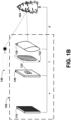
- Figure 3A is an illustration of a noise limiting system 300 that includes an aperture and a waveguide array, according to example embodiments.
- system 300 can be used with LIDAR device 200 instead of or in addition to system 290.
- system 300 may measure light 302 scattered by an object 304 within a scene, similarly to, respectively, system 100, light 102, and object 104.
- system 300 includes light detector arrays 310, 316, and 318, each of which may be similar to light detector array 110.
- light detector array 310 may include a plurality of light detectors, similar to detectors 112 and 114, arranged to intercept and/or detect diverging light portion 302a incident on array 310.
- outputs from the light detectors in array 310 can be combined (e.g., parallel circuit connection, computation via controller 250, etc.) similarly to outputs of the light detectors in array 110.
- system 300 can increase the detection area (shown as shaded region of array 310) for detecting light 302a, as compared to a corresponding cross-sectional area of light portion 302a at aperture 322.
- system 300 also includes an opaque material 320, an aperture 322, and a lens 330, which may be similar, respectively, to opaque material 120, aperture 122, and lens 130.
- aperture 322 is shown to have a different shape (elliptical) compared to a shape of aperture 122 (rectangular).
- system 300 also includes a waveguide array 360 interposed between aperture 322 and arrays 310, 316, 318.
- Waveguide array 360 may include a plurality of waveguides (not shown) arranged to receive light 302 transmitted through aperture 322 and projected onto a receiving side 360a of array 360 (shown as shaded region of side 360a).
- Figure 3B illustrates a cross-section view of system 300, according to example embodiments.
- waveguide array 360 includes cladding layers 362, 366, 372, 376, 382, and 386, core layers 364, 374, and 384, and absorbing layers 368 and 378.
- Cladding layers 362, 366, 372, 376, 382, and 386 may comprise a relatively low index of refraction material, such as polymer coated or fluorine-doped glass substrates for instance.
- Core layers 364, 374, and 384 may comprise a relatively high index of refraction material, such as a glass or high-index polymer substrate for instance, that is transparent to at least some wavelengths of light 302.
- Absorbing layers 368 and 378 may comprise an absorber formed from any material suitable for absorbing wavelengths of light 302 guided within waveguide array 360. To that end, a non-exhaustive list of example absorbers includes carbon black, black chrome, among others.
- waveguide array 360 can be formed from a glass substrate that includes doped regions corresponding to cladding layers 362, 366, 372, 376, and 386. Thus, regions of the glass substrate that are not doped may correspond to core layers 364, 374, and 378.
- a first waveguide of the plurality of waveguides in array 360 may comprise cladding 362, core 364, and cladding 366.
- a second waveguide may comprise cladding 372, core 374, and cladding 376.
- a third waveguide may comprise cladding 382, core 384, and cladding 386.
- each waveguide in array 360 may have a respective input end (e.g., exposed surface of respective core) along a surface of side 360a, and a respective output end (e.g., another exposed surface of respective core) along a surface of output side 360b (opposite to side 360a).
- the waveguides in array 360 can have predefined dimensions based on the size of aperture 322, the distance between aperture 322 and lens 330, and characteristics of lens 330 (e.g., focal length), among other factors.
- the waveguides in array 360 may also be stacked or otherwise aligned with aperture 322 such that each waveguide receives a respective portion of light 302 projected onto side 360a.
- the waveguides in array 360 may be in a stack arrangement parallel to a lengthwise direction (e.g., long axis) of aperture 322 (e.g., vertically stacked between sides 360c and 360d).
- the first waveguide may receive a portion of light 302 projected on side 360a and extending between cladding layers 362 and 366 (i.e., input end of the first waveguide). The first waveguide may then guide the first portion of light 302, via total internal reflection for instance, toward and out of an output end of the first waveguide (e.g., surface of core 364 at side 360b) as first diverging light portion 302a.
- light detector array 310 may be positioned adjacent to the output end of the first waveguide to intercept and detect diverging light portion 302a.
- the second waveguide can guide second diverging light portion 302b toward light detector array 316
- the third waveguide can guide third diverging light portion 302c toward light detector array 318.
- each waveguide may extend vertically (e.g., parallel to a long axis of aperture 322) between sides 360c and 360d, and horizontally (e.g., parallel to a short axis of aperture 322 which points out of the page in Figure 3B ) between side 360e and another side of array 360 opposite to side 360e.
- each waveguide may reduce divergence (e.g., due to reflection of guided light at the cladding layers, etc.) in a stacking direction (e.g., vertically) of the waveguides, while allowing a greater extent of divergence in a direction perpendicular to the stacking direction (e.g., horizontally).
- array 360 may prevent overlap between respective diverging light portions 302a, 302b, 302c guided in the adjacent waveguides while increasing the respective detection areas at the light detector arrays relative to a cross-sectional area of aperture 322.
- system 300 can capture a multi-pixel image of the scene by detecting light portions incident on each light detector array 310, 316, 318 separately and simultaneously.
- each output from a light detector array may correspond to an image pixel of a vertical arrangement of pixels representating the scene.
- the image pixel is detected over a larger cross-sectional area than a cross-sectional area of a portion of light 302 entering a respective input end.
- waveguide array 360 can be employed as an optical diffuser that distributes the power density of light 302 transmitted through aperture 322 among the various light detector arrays.
- the guided light portions may leak to an adjacent waveguide.
- such leakage may be due to an angle of incidence of the guided light at an interface between cladding 366 and core 364 approaching the critical angle.
- guided light in the first waveguide may potentially leak through cladding 366 as an evanescent field evanescing toward the second waveguide.
- absorbing layer 368 includes an absorber (e.g., carbon black) that has a suitable thickness to absorb the evanescent field evanescing from the first waveguide and/or the second waveguide.
- absorbing layer 378 may be configured to absorb evanescing light between the second and third waveguides.
- a core of a waveguide in array 360 can be surrounded by cladding layers along all sides of the core other than the exposed input end and output end of the waveguide.
- cladding 362 may extend around core 364 at side 360e (and an opposite side of array 360) to connect with cladding layer 366.
- the first waveguide may be configured as a non-planar waveguide that provides two-dimensional transverse optical confinement of light portion 302a guided inside the first waveguide.
- the core can be sandwiched between planar cladding layers along only two sides of the core.
- cladding layers 372 and 376 may be disposed along two opposite sides of core 374 but not along side 360e (and an opposite side thereof) of array 360.
- the second waveguide may be configured as a planar waveguide that provides optical confinement in only one transverse direction of light portion 302b guided inside the second waveguide.
- system 300 may include fewer or more components than those shown. Further, in some embodiments, one or more of the components shown can be combined, or divided into separate components.
- light detector arrays 310, 316, 318 are shown to be disposed at a distance from side 360b of waveguide array 360, one or more of light detector arrays 310, 316, 318 can be alternatively disposed on side 360b.
- array 310 can be disposed (e.g., molded, etc.) on the output end (exposed surface of core 364) of the first waveguide
- light detector array 316 can be disposed on the output end (exposed surface of core 374) of the second waveguide
- light detector 318 can be disposed on the output end (exposed surface of core 384) of the third waveguide.
- a distance between waveguide array 360 and aperture 322 can vary.
- waveguide array 360 can be disposed along (e.g., in contact with, etc.) opaque material 320.
- input ends of the waveguides in array 360 can be substantially coplanar with aperture 322.
- aperture 322 can be configured as a limiting aperture in one direction (e.g., parallel to long axis or lengthwise direction of aperture 322), and the input ends of the waveguides in array 360 can be configured as limiting apertures in another direction (e.g., parallel to short axis or widthwise direction of aperture 322).
- waveguide array 360 can guide light portions 302a, 302b, 302c prior to divergence and/or mixing of the light portions after being transmitted through aperture 302.
- waveguide array 360 can be alternatively positioned at a distance (e.g., gap) from opaque material 320 (and aperture 322).
- the outputs of light detector arrays 310, 316, 318 can be processed (e.g., via controller 250) to account for divergence / mixing of light 302 transmitted through aperture 322.
- the arrangement of aperture 322 (and/or side 360a of array 360) relative to lens 330 can vary.
- aperture 322 (and/or input ends of the waveguides in array 360) can be disposed along the focal plane of lens 330.
- aperture 322 (and/or input ends of the waveguides in array 360) can be disposed parallel to the focal plane of lens 330 but at a different distance to lens 330 than the distance between the focal plane and lens 330.
- optical characteristics e.g., focus configuration, etc.
- system 300 may also include an actuator that moves lens 330, opaque material 320, and/or array 360 to achieve a particular optical configuration while scanning the scene.
- opaque material 320 can be omitted from system 300.
- each respective input end of the waveguides in array 360 may correspond to a respective aperture of system 300.
- waveguide array 360 is shown as a single physical structure, the waveguides in array 360 can be alternatively implemented as separate physical structures, and the separate physical waveguides can be stacked (e.g., vertically) with absorbers 368 and 378 appropriately interposed between the various waveguides.
- the waveguides can be implemented as glass plates that are stacked on top of one another in a stacking direction parallel to the lengthwise direction of aperture 322.
- one or more of cladding layers 362, 366, 372, 376, 382, 386, and/or absorbers 368, 378 can be omitted.
- the thickness of any of cladding layers 362, 366, 372, 376, 382, and/or absorbers 368, 378 can be varied between sides 360a and 360b.
- the cladding layers (and/or the absorbers) can have a smaller thickness near side 360a relative to a corresponding thickness near side 360b (e.g., gradually increased, tapered, etc.).
- a larger extent of light 302 incident on side 360a can be projected onto the exposed surfaces of cores 364, 374, 384, and thereby guided through the waveguides in array 360 toward light detector arrays 310, 316, 318.
- waveguide array 360 may include fewer or more than the three waveguides shown.
- light detector arrays 310, 316, 318 are shown as separate physical structures, light detector arrays 310, 316, 318 can be alternatively implemented on a single physical substrate, where one or more rows of light detectors are connected to one another but not to other rows of light detectors in the single substrate.
- a device that controls system 300 can be configured to combine outputs from two or more light detector arrays to increase the detection area as well as the effective aperture size associated with the combined detected light portions.
- outputs from arrays 310 and 316 can be combined such that a larger effective aperture size corresponding to two portions of light 302 incident on two input ends of the first and second waveguides can be achieved, as opposed to a smaller effective aperture size that corresponds to a single light portion incident on only one of the two input ends.
- Figure 4 is a flowchart of a method 400, according to example embodiments.
- Method 400 presents an embodiment of a method that could be used with any of systems 100, 300, and/or device 200, for example.
- Method 400 may include one or more operations, functions, or actions as illustrated by one or more of blocks 402-410. Although the blocks are illustrated in a sequential order, these blocks may in some instances be performed in parallel, and/or in a different order than those described herein. Also, the various blocks may be combined into fewer blocks, divided into additional blocks, and/or removed based upon the desired implementation.
- each block may represent a module, a segment, a portion of a manufacturing or operation process, or a portion of program code, which includes one or more instructions executable by a processor for implementing specific logical functions or steps in the process.
- the program code may be stored on any type of computer readable medium, for example, such as a storage device including a disk or hard drive.
- the computer readable medium may include a non-transitory computer readable medium, for example, such as computer-readable media that stores data for short periods of time like register memory, processor cache and Random Access Memory (RAM).
- the computer readable medium may also include non-transitory media, such as secondary or persistent long term storage, like read only memory (ROM), optical or magnetic disks, compact-disc read only memory (CD-ROM), for example.
- the computer readable media may also be any other volatile or nonvolatile storage systems.
- the computer readable medium may be considered a computer readable storage medium, for example, or a tangible storage device.
- each block in Figure 4 may represent circuitry that is wired to perform the specific logical functions in the process.
- method 400 involves focusing, by a lens (e.g., lens 130) disposed relative to a scene, light from the scene toward a focal plane of the lens.
- a lens e.g., lens 130
- the light from the scene may be scattered by an object (e.g., object 104) within the scene.
- a computing device e.g., controller 250
- method 400 involves transmitting, through an aperture (e.g., aperture 122) defined within an opaque material (e.g., opaque material 120), the focused light from the scene.
- an aperture e.g., aperture 122
- an opaque material e.g., opaque material 120
- method 400 involves receiving, at an input end of a given waveguide of a plurality of waveguides, a portion of the light transmitted through the aperture.
- method 400 involves guiding, by the given waveguide, the received portion of the light toward an output end of the given waveguide.
- method 400 involves detecting, via an array of light detectors, the guided light propagating out of the output end.
- a cross-sectional area of the detected light may be greater than a cross-sectional area of the portion of the light received at the input end.
Landscapes
- Physics & Mathematics (AREA)
- General Physics & Mathematics (AREA)
- Engineering & Computer Science (AREA)
- Computer Networks & Wireless Communication (AREA)
- Radar, Positioning & Navigation (AREA)
- Remote Sensing (AREA)
- Optics & Photonics (AREA)
- Electromagnetism (AREA)
- Spectroscopy & Molecular Physics (AREA)
- Measurement Of Optical Distance (AREA)
- Optical Radar Systems And Details Thereof (AREA)
- Investigating Or Analysing Materials By Optical Means (AREA)
- Photometry And Measurement Of Optical Pulse Characteristics (AREA)
Claims (14)
- System (300), umfassend:eine Linse (330), die relativ zu einer Szene angeordnet und so konfiguriert ist, dass sie Licht von der Szene auf eine Brennebene der Linse fokussiert;eine Apertur (322), die in einem opaken Material definiert ist, parallel zu der Brennebene der Linse angeordnet, wobei von der Linse fokussiertes Licht durch die Apertur hindurch übertragen wird;eine Vielzahl von Wellenleitern (360),wobei ein erster bestimmter Wellenleiter der Vielzahl ein Eingangsende aufweist, das so konfiguriert ist, dass es einen ersten Teil von Licht empfängt, das durch einen ersten Teil der Apertur übertragen wird, wobei der erste bestimmte Wellenleiter so konfiguriert ist, dass er den empfangenen ersten Teil des Lichts zur Übertragung durch ein Ausgangsende des ersten bestimmten Wellenleiters leitet;wobei ein zweiter bestimmter Wellenleiter der Vielzahl ein Eingangsende aufweist, das konfiguriert ist, einen zweiten Teil von Licht zu empfangen, das durch einen zweiten Teil der Apertur übertragen wird, wobei der zweite bestimmte Wellenleiter konfiguriert ist, den empfangenen zweiten Teil des Lichts zur Übertragung durch ein Ausgangsende des zweiten bestimmten Wellenleiters zu leiten; unddadurch gekennzeichnet, dass der erste und der zweite bestimmte Wellenleiter so konfiguriert sind, dass sie die Divergenz des ersten und des zweiten Teils des darin geleiteten Lichts so begrenzen, dass jeder geleitete Teil des Lichts einen anderen geleiteten Teil des Lichts innerhalb eines angrenzenden Wellenleiters der Vielzahl von Wellenleitern nicht überschneidet;eine Vielzahl von Anordnungen von Lichtdetektoren (310, 316, 318),wobei eine erste Anordnung der Vielzahl von Anordnungen so konfiguriert ist, dass sie das geleitete Licht erfasst, das durch das Ausgangsende des ersten bestimmten Wellenleiters übertragen wird, wobei eine Querschnittsfläche eines Erfassungsbereichs der ersten Anordnung, die konfiguriert ist, das durch das Ausgangsende des ersten bestimmten Wellenleiters übertragene geleitete Licht zu erfassen, größer ist als eine Querschnittsfläche des empfangenen ersten Teils des Lichts an dem Eingangsende des ersten bestimmten Wellenleiters; undwobei eine zweite Anordnung der Vielzahl von Anordnungen so konfiguriert ist, dass sie das geleitete Licht erfasst, das durch das Ausgangsende des zweiten bestimmten Wellenleiters übertragen wird, wobei eine Querschnittsfläche eines Erfassungsbereichs der zweiten Anordnung, die konfiguriert ist, das durch das Ausgangsende des zweiten bestimmten Wellenleiters übertragene geleitete Licht zu erfassen, größer ist als eine Querschnittsfläche des empfangenen zweiten Teils des Lichts an dem Eingangsende des zweiten bestimmten Wellenleiters.
- System nach Anspruch 1, wobei der erste und der zweite bestimmte Wellenleiter konfiguriert sind, die Divergenz des geleiteten Lichts entlang einer Längsrichtung der Apertur zu reduzieren.
- System nach Anspruch 1, wobei die Vielzahl von Wellenleitern in einer Stapelanordnung angeordnet ist, und wobei die bestimmten Wellenleiter konfiguriert sind, die Divergenz des geleiteten Lichts entlang einer Stapelungsrichtung der Stapelanordnung zu reduzieren;
optional, wobei die Vielzahl von Wellenleitern eine planare Wellenleiteranordnung umfasst, und wobei die Stapelungsrichtung parallel zu einer Längsrichtung der Apertur ist. - System nach Anspruch 1, wobei die erste und die zweite Anordnung von Lichtdetektoren eine Vielzahl von Einzelphotonen-Lawinendioden (SPADs) umfassen; und/oder
wobei die Lichtdetektoren in jeder der Anordnungen parallel miteinander verbunden sind. - System nach Anspruch 1, wobei die erste Anordnung von Lichtdetektoren an dem Ausgangsende des ersten bestimmten Wellenleiters angeordnet ist, und wobei die zweite Anordnung von Lichtdetektoren an dem Ausgangsende des zweiten bestimmten Wellenleiters angeordnet ist.
- System nach Anspruch 1, wobei das Ausgangsende des ersten bestimmten Wellenleiters dem Eingangsende des ersten bestimmten Wellenleiters gegenüberliegt und wobei das Ausgangsende des zweiten bestimmten Wellenleiters dem Eingangsende des zweiten bestimmten Wellenleiters gegenüberliegt.
- System nach Anspruch 1, wobei die Vielzahl von Wellenleitern Folgendes umfasst:einen ersten Kern, der einen ersten Brechungsindex aufweist;einen zweiten Kern, der den ersten Brechungsindex aufweist; undeine Ummantelung, die zumindest teilweise zwischen dem ersten Kern und dem zweiten Kern angeordnet ist, wobei die Ummantelung einen zweiten Brechungsindex aufweist, der niedriger als der erste Brechungsindex ist.
- System nach Anspruch 7, wobei das Eingangsende des ersten bestimmten Wellenleiters der Vielzahl von Wellenleitern einer Oberfläche des ersten Kerns, angrenzend an die Apertur, entspricht, und wobei das Eingangsende des zweiten bestimmten Wellenleiters der Vielzahl von Wellenleitern einer Oberfläche des zweiten Kerns, angrenzend an die Apertur, entspricht;
wobei die Ummantelung optional entlang einer Vielzahl von Seiten des ersten Kerns angeordnet ist, mit Ausnahme von: (i) einer ersten Seite, die das Eingangsende des ersten bestimmten Wellenleiters beinhaltet, und (ii) einer zweiten Seite, die das Ausgangsende des ersten bestimmten Wellenleiters beinhaltet. - System nach Anspruch 7, ferner umfassend einen Absorber, der zwischen dem ersten Kern und dem zweiten Kern angeordnet ist, wobei der Absorber so konfiguriert ist, dass er verhindert, dass sich evaneszentes Licht, das sich von dem ersten Kern durch die Ummantelung verflüchtigt, in den zweiten Kern ausbreitet.
- System nach Anspruch 7, wobei die Vielzahl von Wellenleitern ein Glassubstrat umfasst, wobei die Ummantelung einem Bereich des Glassubstrats entspricht, der dotiert ist, um einen niedrigeren Brechungsindex relativ zu angrenzenden Bereichen des Glassubstrats aufzuweisen, wobei der erste Kern einem Bereich des Glassubstrats entspricht, der nicht dotiert ist.
- Verfahren, umfassend:Fokussieren, mittels einer Linse (330), die relativ zu einer Szene angeordnet ist, von Licht von der Szene in Richtung einer Brennebene;Übertragen, durch eine Apertur (322), die innerhalb eines opaken Materials parallel zu der Brennebene definiert ist, des fokussierten Lichts von der Szene;Empfangen, an einem Eingangsende eines ersten bestimmten Wellenleiters einer Vielzahl von Wellenleitern (360), eines ersten Teils des durch die Apertur übertragenen Lichts;Empfangen, an einem Eingangsende eines zweiten bestimmten Wellenleiters der Vielzahl von Wellenleitern, eines zweiten Teils des durch die Apertur übertragenen Lichts;Leiten, durch den ersten bestimmten Wellenleiter, des empfangenen ersten Teils des Lichts in Richtung eines Ausgangsendes des ersten bestimmten Wellenleiters;Leiten, durch den zweiten bestimmten Wellenleiter, des empfangenen zweiten Teils des Lichts in Richtung eines Ausgangsendes des zweiten bestimmten Wellenleiters, dadurch gekennzeichnet, dass der erste und der zweite bestimmte Wellenleiter die Divergenz des ersten und des zweiten Teils des darin geleiteten Lichts derart begrenzen, dass jeder geleitete Teil des Lichts einen anderen geleiteten Teil des Lichts innerhalb eines angrenzenden Wellenleiters der Vielzahl von Wellenleitern nicht überschneidet;Erfassen, an einer ersten Anordnung von Lichtdetektoren (310, 316, 318), des sich aus dem Ausgangsende des ersten bestimmten Wellenleiters ausbreitenden geleiteten Lichts, wobei eine Querschnittsfläche des erfassten Lichts größer ist als eine Querschnittsfläche des ersten Teils des Lichts, das an dem Eingangsende des ersten bestimmten Wellenleiters empfangen wird; undErfassen, an einer zweiten Anordnung von Lichtdetektoren (310, 316, 318), des sich aus dem Ausgangsende des zweiten bestimmten Wellenleiters ausbreitenden geleiteten Lichts, wobei eine Querschnittsfläche des erfassten Lichts größer ist als eine Querschnittsfläche des zweiten Teils des Lichts, das an dem Eingangsende des zweiten bestimmten Wellenleiters empfangen wird.
- Verfahren nach Anspruch 11, ferner umfassend, für jede der ersten und zweiten Anordnung, Kombinieren von Ausgaben von den Lichtdetektoren in der Anordnung basierend darauf, dass die Lichtdetektoren in der Anordnung parallel miteinander verbunden sind.
- Verfahren nach Anspruch 12, ferner umfassend:Senden, mittels eines Lichtemitters, eines Lichtimpulses in Richtung der Szene;Erfassen einer Reflexion des Lichtimpulses basierend auf den kombinierten Ausgaben von den Lichtdetektoren; undBestimmen eines Orts eines Objekts in der Szene basierend auf zumindest der erfassten Reflexion.
- Lichtdetektions- und Entfernungsmess(LIDAR)-Vorrichtung (200), umfassend:einen LIDAR-Empfänger, der das System nach einem der Ansprüche 1-10 umfasst, wobei der LIDAR-Empfänger konfiguriert ist, Licht zu empfangen, das von einem oder mehreren Objekten innerhalb der Szene gestreut wird; undeinen LIDAR-Sender, der konfiguriert ist, die Szene zu beleuchten.
Applications Claiming Priority (2)
| Application Number | Priority Date | Filing Date | Title |
|---|---|---|---|
| US15/366,746 US10605984B2 (en) | 2016-12-01 | 2016-12-01 | Array of waveguide diffusers for light detection using an aperture |
| PCT/US2017/064104 WO2018102628A1 (en) | 2016-12-01 | 2017-12-01 | Array of waveguide diffusers for light detection using an aperture |
Publications (3)
| Publication Number | Publication Date |
|---|---|
| EP3529571A1 EP3529571A1 (de) | 2019-08-28 |
| EP3529571A4 EP3529571A4 (de) | 2020-06-24 |
| EP3529571B1 true EP3529571B1 (de) | 2025-03-26 |
Family
ID=62242696
Family Applications (1)
| Application Number | Title | Priority Date | Filing Date |
|---|---|---|---|
| EP17875659.9A Active EP3529571B1 (de) | 2016-12-01 | 2017-12-01 | Anordnung aus wellenleiterdiffusoren zur lichtdetektion mit einer apertur |
Country Status (6)
| Country | Link |
|---|---|
| US (3) | US10605984B2 (de) |
| EP (1) | EP3529571B1 (de) |
| JP (1) | JP6821024B2 (de) |
| KR (1) | KR102469158B1 (de) |
| CN (2) | CN110036264B (de) |
| WO (1) | WO2018102628A1 (de) |
Families Citing this family (21)
| Publication number | Priority date | Publication date | Assignee | Title |
|---|---|---|---|---|
| US10605984B2 (en) | 2016-12-01 | 2020-03-31 | Waymo Llc | Array of waveguide diffusers for light detection using an aperture |
| US10502618B2 (en) | 2016-12-03 | 2019-12-10 | Waymo Llc | Waveguide diffuser for light detection using an aperture |
| TW201823675A (zh) * | 2016-12-27 | 2018-07-01 | 鴻海精密工業股份有限公司 | 一種鐳射發射接收裝置以及鐳射探測與測量系統 |
| JP7154230B2 (ja) * | 2017-05-15 | 2022-10-17 | アウスター インコーポレイテッド | 輝度を増強した光学撮像送信器 |
| US11340336B2 (en) | 2017-12-07 | 2022-05-24 | Ouster, Inc. | Rotating light ranging system with optical communication uplink and downlink channels |
| CN112105975A (zh) * | 2018-01-14 | 2020-12-18 | 光场实验室公司 | 用于能量中继器中使用有序结构进行横向能量局域化的系统和方法 |
| JP6519033B1 (ja) * | 2018-07-03 | 2019-05-29 | Dolphin株式会社 | 物体検出装置、物体検出方法、および物体検出装置の設計方法 |
| US11520044B2 (en) | 2018-09-25 | 2022-12-06 | Waymo Llc | Waveguide diffusers for LIDARs |
| US20220357451A1 (en) * | 2019-03-05 | 2022-11-10 | Waymo Llc | Lidar transmitter/receiver alignment |
| JP6651110B1 (ja) | 2019-05-28 | 2020-02-19 | Dolphin株式会社 | 物体検出装置 |
| US11156699B2 (en) | 2019-10-29 | 2021-10-26 | Waymo Llc | Multilayer optical devices and systems |
| US11385406B2 (en) | 2019-10-29 | 2022-07-12 | Waymo Llc | Optical signal routing devices and systems |
| EP3839425A1 (de) * | 2019-12-16 | 2021-06-23 | Hilti Aktiengesellschaft | Verfahren zum bestimmen eines abstandes zwischen einem lasersystem und einer projektionsfläche |
| US12352900B2 (en) * | 2019-12-20 | 2025-07-08 | Waymo Llc | Light detection and ranging (lidar) device having a light-guide manifold |
| US12468020B2 (en) | 2019-12-27 | 2025-11-11 | Waymo Llc | Optical redirector device |
| JP7474853B2 (ja) * | 2019-12-27 | 2024-04-25 | ウェイモ エルエルシー | 光リダイレクタデバイス |
| EP4222532A4 (de) * | 2020-10-23 | 2024-10-02 | Sense Photonics, Inc. | Integriertes weitbereichs-festkörper-flash-lidar-system mit schmalem fov und kurzer reichweite |
| JP2022167122A (ja) * | 2021-04-22 | 2022-11-04 | 京セラ株式会社 | 電磁波検出装置 |
| US11947050B2 (en) * | 2021-07-07 | 2024-04-02 | Beijing Voyager Technology Co., Ltd. | Temperature control through thermal recycle |
| US12444068B2 (en) | 2022-08-01 | 2025-10-14 | Lg Innotek Co., Ltd. | Optical inspection based on repetitive feature comparison |
| CN118112588A (zh) * | 2022-11-29 | 2024-05-31 | 深圳市速腾聚创科技有限公司 | 激光雷达及可移动设备 |
Family Cites Families (58)
| Publication number | Priority date | Publication date | Assignee | Title |
|---|---|---|---|---|
| US3899145A (en) | 1973-07-20 | 1975-08-12 | Us Navy | Laser transmitting and receiving lens optics |
| JPS6111693Y2 (de) * | 1977-03-14 | 1986-04-12 | ||
| JPS5942507A (ja) | 1982-09-03 | 1984-03-09 | Nippon Kogaku Kk <Nikon> | 焦点検出装置 |
| US5159412A (en) | 1991-03-15 | 1992-10-27 | Therma-Wave, Inc. | Optical measurement device with enhanced sensitivity |
| JPH0694573A (ja) * | 1992-09-11 | 1994-04-05 | Nikon Corp | 導波路デバイスの信号処理回路 |
| US5391869A (en) | 1993-03-29 | 1995-02-21 | United Technologies Corporation | Single-side growth reflection-based waveguide-integrated photodetector |
| US5764842A (en) * | 1995-03-23 | 1998-06-09 | Hitachi, Ltd. | Semiconductor guided-wave optical device and method of fabricating thereof |
| US5608833A (en) * | 1995-07-20 | 1997-03-04 | Hughes Electronics | Focal-plane detector imaging system with improved optical damage threshold |
| US6584052B1 (en) | 1998-06-02 | 2003-06-24 | Science Applications International Corporation | Method and apparatus for controlling the focus of a read/write head for an optical scanner |
| JP4184570B2 (ja) | 2000-04-18 | 2008-11-19 | セイコーインスツル株式会社 | 情報記録再生装置 |
| JP4284892B2 (ja) | 2001-07-13 | 2009-06-24 | オムロン株式会社 | 多分岐光導波路 |
| US20030034491A1 (en) | 2001-08-14 | 2003-02-20 | Motorola, Inc. | Structure and method for fabricating semiconductor structures and devices for detecting an object |
| JP2003227976A (ja) * | 2001-11-30 | 2003-08-15 | Yazaki Corp | プラスチック光ファイバおよび光ファイバケーブル |
| AU2003241557A1 (en) | 2002-05-17 | 2003-12-02 | Arete Associates | Micromechanical and related lidar apparatus and method, and fast light-routing components |
| US7351977B2 (en) * | 2002-11-08 | 2008-04-01 | L-3 Communications Cincinnati Electronics Corporation | Methods and systems for distinguishing multiple wavelengths of radiation and increasing detected signals in a detection system using micro-optic structures |
| JP2004207479A (ja) | 2002-12-25 | 2004-07-22 | Pioneer Electronic Corp | 半導体レーザ装置及びその製造方法 |
| US7038191B2 (en) * | 2003-03-13 | 2006-05-02 | The Boeing Company | Remote sensing apparatus and method |
| CA2490603C (en) | 2003-12-24 | 2012-12-11 | National Research Council Of Canada | Optical off-chip interconnects in multichannel planar waveguide devices |
| KR20070100729A (ko) * | 2004-12-14 | 2007-10-11 | 오엠에스 디스플레이스 리미티드 | 광학적 크기변경을 위한 디바이스 및 방법 |
| WO2006102917A1 (en) | 2005-03-31 | 2006-10-05 | Pirelli & C. S.P.A. | Method to fabricate a redirecting mirror in optical waveguide devices |
| CA2620948A1 (en) | 2005-09-02 | 2007-03-08 | Neptec | Apparatus and method for tracking an object |
| WO2007046100A2 (en) | 2005-10-18 | 2007-04-26 | Oms Displays Ltd. | Device and method for optical resizing and backlighting |
| US8190030B2 (en) | 2005-11-10 | 2012-05-29 | Optical Air Data Systems, Llc | Single aperture multiple optical waveguide transceiver |
| US7564190B2 (en) * | 2006-06-09 | 2009-07-21 | Victor Company Of Japan, Ltd. | Light source device and image displaying apparatus using the same |
| JP5018254B2 (ja) | 2007-06-06 | 2012-09-05 | 日立電線株式会社 | ミラー付き光導波路及びその製造方法 |
| KR101016281B1 (ko) * | 2007-07-10 | 2011-02-22 | 엘지디스플레이 주식회사 | 수평 전계 인가형 박막 트랜지스터 어레이 |
| US7894058B2 (en) * | 2008-01-11 | 2011-02-22 | California Institute Of Technology | Single-lens computed tomography imaging spectrometer and method of capturing spatial and spectral information |
| EP3396416A1 (de) * | 2008-11-25 | 2018-10-31 | Tetravue, Inc. | Systeme und verfahren für dreidimensionale bildgebung mit hoher auflösung |
| WO2010124028A2 (en) | 2009-04-21 | 2010-10-28 | Vasylyev Sergiy V | Light collection and illumination systems employing planar waveguide |
| US8149654B2 (en) * | 2010-03-23 | 2012-04-03 | Tdk Corporation | Wave guide that attenuates evanescent light of higher order TM mode |
| US9028123B2 (en) | 2010-04-16 | 2015-05-12 | Flex Lighting Ii, Llc | Display illumination device with a film-based lightguide having stacked incident surfaces |
| US8797512B2 (en) * | 2011-09-15 | 2014-08-05 | Advanced Scientific Concepts, Inc. | Automatic range corrected flash ladar camera |
| EP2831497B1 (de) * | 2012-03-29 | 2025-05-07 | École Polytechnique Fédérale de Lausanne (EPFL) | Verfahren und vorrichtung für bildgebung mit multimodalen glasfasern |
| CA2871502C (en) | 2012-04-26 | 2021-06-08 | Neptec Design Group Ltd. | High speed 360 degree scanning lidar head |
| DE102013222963B4 (de) * | 2012-11-12 | 2022-07-21 | Fraunhofer-Gesellschaft zur Förderung der angewandten Forschung e.V. | Radarantenne |
| CN105210175A (zh) | 2012-11-12 | 2015-12-30 | 德玛雷有限责任公司 | 绝热的平面波导耦合器转换器 |
| US9823351B2 (en) | 2012-12-18 | 2017-11-21 | Uber Technologies, Inc. | Multi-clad fiber based optical apparatus and methods for light detection and ranging sensors |
| EP2936222B1 (de) | 2012-12-18 | 2019-07-03 | Pacific Biosciences Of California, Inc. | Eine optische analysevorrichtung |
| US9322992B2 (en) | 2013-01-29 | 2016-04-26 | Vencore Labs, Inc. | Devices and methods for multimode light detection |
| US8836922B1 (en) | 2013-08-20 | 2014-09-16 | Google Inc. | Devices and methods for a rotating LIDAR platform with a shared transmit/receive path |
| DE102014102420A1 (de) * | 2014-02-25 | 2015-08-27 | Sick Ag | Optoelektronischer Sensor und Verfahren zur Objekterfassung in einem Überwachungsbereich |
| US9360554B2 (en) | 2014-04-11 | 2016-06-07 | Facet Technology Corp. | Methods and apparatus for object detection and identification in a multiple detector lidar array |
| US9575341B2 (en) | 2014-06-28 | 2017-02-21 | Intel Corporation | Solid state LIDAR circuit with waveguides tunable to separate phase offsets |
| EP3218749A2 (de) | 2014-11-11 | 2017-09-20 | Finisar Corporation | Zweistufige adiabatisch gekoppelte fotonische systeme |
| EP3247970A4 (de) | 2015-01-20 | 2018-12-19 | Torrey Pines Logic, Inc. | Einzelaperturlaserentfernungsmesser |
| US10036801B2 (en) | 2015-03-05 | 2018-07-31 | Big Sky Financial Corporation | Methods and apparatus for increased precision and improved range in a multiple detector LiDAR array |
| CN106291580B (zh) | 2015-06-12 | 2019-08-23 | 上海珏芯光电科技有限公司 | 激光雷达成像系统 |
| EP3130950A1 (de) | 2015-08-10 | 2017-02-15 | Multiphoton Optics Gmbh | Strahlumlenkelement sowie optisches bauelement mit strahlumlenkelement |
| US9992477B2 (en) * | 2015-09-24 | 2018-06-05 | Ouster, Inc. | Optical system for collecting distance information within a field |
| JP6644892B2 (ja) | 2015-12-20 | 2020-02-12 | アップル インコーポレイテッドApple Inc. | 光検出測距センサ |
| US9948866B2 (en) | 2016-02-01 | 2018-04-17 | The Boeing Company | Systems and methods for protecting against high-radiant-flux light based on time-of-flight |
| WO2018039273A1 (en) | 2016-08-22 | 2018-03-01 | Magic Leap, Inc. | Dithering methods and apparatus for wearable display device |
| DE102016118471A1 (de) | 2016-09-29 | 2018-03-29 | Valeo Schalter Und Sensoren Gmbh | Erfassungsvorrichtung für ein Kraftfahrzeug, Anbauteil sowie Kraftfahrzeug |
| US10168494B2 (en) | 2016-11-30 | 2019-01-01 | International Business Machines Corporation | Off-axis micro-mirror arrays for optical coupling in polymer waveguides |
| US10605984B2 (en) | 2016-12-01 | 2020-03-31 | Waymo Llc | Array of waveguide diffusers for light detection using an aperture |
| US10502618B2 (en) * | 2016-12-03 | 2019-12-10 | Waymo Llc | Waveguide diffuser for light detection using an aperture |
| CN108873326A (zh) | 2017-05-16 | 2018-11-23 | 中强光电股份有限公司 | 头戴式显示装置 |
| DE102017211910A1 (de) | 2017-07-12 | 2019-01-17 | Dr. Johannes Heidenhain Gmbh | Diffraktiver Biosensor |
-
2016
- 2016-12-01 US US15/366,746 patent/US10605984B2/en active Active
-
2017
- 2017-12-01 WO PCT/US2017/064104 patent/WO2018102628A1/en not_active Ceased
- 2017-12-01 KR KR1020197018521A patent/KR102469158B1/ko active Active
- 2017-12-01 JP JP2019527865A patent/JP6821024B2/ja active Active
- 2017-12-01 CN CN201780074785.9A patent/CN110036264B/zh active Active
- 2017-12-01 CN CN202110789574.1A patent/CN113625248B/zh active Active
- 2017-12-01 EP EP17875659.9A patent/EP3529571B1/de active Active
-
2020
- 2020-03-26 US US16/830,680 patent/US11714171B2/en active Active
-
2023
- 2023-06-12 US US18/333,074 patent/US12111422B2/en active Active
Also Published As
| Publication number | Publication date |
|---|---|
| US20230324523A1 (en) | 2023-10-12 |
| KR20190077625A (ko) | 2019-07-03 |
| JP2020501133A (ja) | 2020-01-16 |
| CN110036264B (zh) | 2021-07-27 |
| US20180156971A1 (en) | 2018-06-07 |
| US12111422B2 (en) | 2024-10-08 |
| CN110036264A (zh) | 2019-07-19 |
| CN113625248B (zh) | 2024-06-04 |
| US20200225410A1 (en) | 2020-07-16 |
| CN113625248A (zh) | 2021-11-09 |
| US10605984B2 (en) | 2020-03-31 |
| EP3529571A4 (de) | 2020-06-24 |
| JP6821024B2 (ja) | 2021-01-27 |
| WO2018102628A1 (en) | 2018-06-07 |
| US11714171B2 (en) | 2023-08-01 |
| EP3529571A1 (de) | 2019-08-28 |
| KR102469158B1 (ko) | 2022-11-22 |
Similar Documents
| Publication | Publication Date | Title |
|---|---|---|
| US12111422B2 (en) | Array of waveguide diffusers for light detection using an aperture | |
| US12078530B2 (en) | Light detection using an aperture | |
| US12461206B2 (en) | LIDAR receiver using a waveguide and an aperture | |
| EP3497413B1 (de) | Begrenzung von rauschen auf lichtdetektoren mithilfe einer öffnung | |
| US12164026B2 (en) | Waveguide diffusers for LIDARs |
Legal Events
| Date | Code | Title | Description |
|---|---|---|---|
| STAA | Information on the status of an ep patent application or granted ep patent |
Free format text: STATUS: THE INTERNATIONAL PUBLICATION HAS BEEN MADE |
|
| PUAI | Public reference made under article 153(3) epc to a published international application that has entered the european phase |
Free format text: ORIGINAL CODE: 0009012 |
|
| STAA | Information on the status of an ep patent application or granted ep patent |
Free format text: STATUS: REQUEST FOR EXAMINATION WAS MADE |
|
| 17P | Request for examination filed |
Effective date: 20190523 |
|
| AK | Designated contracting states |
Kind code of ref document: A1 Designated state(s): AL AT BE BG CH CY CZ DE DK EE ES FI FR GB GR HR HU IE IS IT LI LT LU LV MC MK MT NL NO PL PT RO RS SE SI SK SM TR |
|
| AX | Request for extension of the european patent |
Extension state: BA ME |
|
| DAV | Request for validation of the european patent (deleted) | ||
| DAX | Request for extension of the european patent (deleted) | ||
| REG | Reference to a national code |
Ref country code: DE Ref legal event code: R079 Free format text: PREVIOUS MAIN CLASS: G01J0001040000 Ipc: G01S0007480000 |
|
| A4 | Supplementary search report drawn up and despatched |
Effective date: 20200525 |
|
| RIC1 | Information provided on ipc code assigned before grant |
Ipc: G02B 6/02 20060101ALI20200516BHEP Ipc: G02B 5/00 20060101ALI20200516BHEP Ipc: G02B 19/00 20060101ALI20200516BHEP Ipc: G01S 17/89 20200101ALI20200516BHEP Ipc: G01S 7/481 20060101ALI20200516BHEP Ipc: G01S 17/02 20200101ALI20200516BHEP Ipc: G01S 7/48 20060101AFI20200516BHEP Ipc: G02B 27/09 20060101ALI20200516BHEP Ipc: G02B 6/08 20060101ALI20200516BHEP |
|
| STAA | Information on the status of an ep patent application or granted ep patent |
Free format text: STATUS: EXAMINATION IS IN PROGRESS |
|
| 17Q | First examination report despatched |
Effective date: 20220425 |
|
| GRAP | Despatch of communication of intention to grant a patent |
Free format text: ORIGINAL CODE: EPIDOSNIGR1 |
|
| STAA | Information on the status of an ep patent application or granted ep patent |
Free format text: STATUS: GRANT OF PATENT IS INTENDED |
|
| INTG | Intention to grant announced |
Effective date: 20241108 |
|
| GRAS | Grant fee paid |
Free format text: ORIGINAL CODE: EPIDOSNIGR3 |
|
| GRAA | (expected) grant |
Free format text: ORIGINAL CODE: 0009210 |
|
| STAA | Information on the status of an ep patent application or granted ep patent |
Free format text: STATUS: THE PATENT HAS BEEN GRANTED |
|
| AK | Designated contracting states |
Kind code of ref document: B1 Designated state(s): AL AT BE BG CH CY CZ DE DK EE ES FI FR GB GR HR HU IE IS IT LI LT LU LV MC MK MT NL NO PL PT RO RS SE SI SK SM TR |
|
| P01 | Opt-out of the competence of the unified patent court (upc) registered |
Free format text: CASE NUMBER: APP_7579/2025 Effective date: 20250213 |
|
| REG | Reference to a national code |
Ref country code: GB Ref legal event code: FG4D |
|
| REG | Reference to a national code |
Ref country code: CH Ref legal event code: EP |
|
| REG | Reference to a national code |
Ref country code: DE Ref legal event code: R096 Ref document number: 602017088583 Country of ref document: DE |
|
| REG | Reference to a national code |
Ref country code: IE Ref legal event code: FG4D |
|
| PG25 | Lapsed in a contracting state [announced via postgrant information from national office to epo] |
Ref country code: RS Free format text: LAPSE BECAUSE OF FAILURE TO SUBMIT A TRANSLATION OF THE DESCRIPTION OR TO PAY THE FEE WITHIN THE PRESCRIBED TIME-LIMIT Effective date: 20250626 |
|
| PG25 | Lapsed in a contracting state [announced via postgrant information from national office to epo] |
Ref country code: FI Free format text: LAPSE BECAUSE OF FAILURE TO SUBMIT A TRANSLATION OF THE DESCRIPTION OR TO PAY THE FEE WITHIN THE PRESCRIBED TIME-LIMIT Effective date: 20250326 |
|
| REG | Reference to a national code |
Ref country code: LT Ref legal event code: MG9D |
|
| PG25 | Lapsed in a contracting state [announced via postgrant information from national office to epo] |
Ref country code: NO Free format text: LAPSE BECAUSE OF FAILURE TO SUBMIT A TRANSLATION OF THE DESCRIPTION OR TO PAY THE FEE WITHIN THE PRESCRIBED TIME-LIMIT Effective date: 20250626 |
|
| PG25 | Lapsed in a contracting state [announced via postgrant information from national office to epo] |
Ref country code: HR Free format text: LAPSE BECAUSE OF FAILURE TO SUBMIT A TRANSLATION OF THE DESCRIPTION OR TO PAY THE FEE WITHIN THE PRESCRIBED TIME-LIMIT Effective date: 20250326 |
|
| PG25 | Lapsed in a contracting state [announced via postgrant information from national office to epo] |
Ref country code: LV Free format text: LAPSE BECAUSE OF FAILURE TO SUBMIT A TRANSLATION OF THE DESCRIPTION OR TO PAY THE FEE WITHIN THE PRESCRIBED TIME-LIMIT Effective date: 20250326 |
|
| PG25 | Lapsed in a contracting state [announced via postgrant information from national office to epo] |
Ref country code: GR Free format text: LAPSE BECAUSE OF FAILURE TO SUBMIT A TRANSLATION OF THE DESCRIPTION OR TO PAY THE FEE WITHIN THE PRESCRIBED TIME-LIMIT Effective date: 20250627 Ref country code: BG Free format text: LAPSE BECAUSE OF FAILURE TO SUBMIT A TRANSLATION OF THE DESCRIPTION OR TO PAY THE FEE WITHIN THE PRESCRIBED TIME-LIMIT Effective date: 20250326 |
|
| REG | Reference to a national code |
Ref country code: NL Ref legal event code: MP Effective date: 20250326 |
|
| PG25 | Lapsed in a contracting state [announced via postgrant information from national office to epo] |
Ref country code: NL Free format text: LAPSE BECAUSE OF FAILURE TO SUBMIT A TRANSLATION OF THE DESCRIPTION OR TO PAY THE FEE WITHIN THE PRESCRIBED TIME-LIMIT Effective date: 20250326 |
|
| PG25 | Lapsed in a contracting state [announced via postgrant information from national office to epo] |
Ref country code: SE Free format text: LAPSE BECAUSE OF FAILURE TO SUBMIT A TRANSLATION OF THE DESCRIPTION OR TO PAY THE FEE WITHIN THE PRESCRIBED TIME-LIMIT Effective date: 20250326 |
|
| REG | Reference to a national code |
Ref country code: AT Ref legal event code: MK05 Ref document number: 1779453 Country of ref document: AT Kind code of ref document: T Effective date: 20250326 |
|
| PG25 | Lapsed in a contracting state [announced via postgrant information from national office to epo] |
Ref country code: SM Free format text: LAPSE BECAUSE OF FAILURE TO SUBMIT A TRANSLATION OF THE DESCRIPTION OR TO PAY THE FEE WITHIN THE PRESCRIBED TIME-LIMIT Effective date: 20250326 |
|
| PG25 | Lapsed in a contracting state [announced via postgrant information from national office to epo] |
Ref country code: ES Free format text: LAPSE BECAUSE OF FAILURE TO SUBMIT A TRANSLATION OF THE DESCRIPTION OR TO PAY THE FEE WITHIN THE PRESCRIBED TIME-LIMIT Effective date: 20250326 Ref country code: PT Free format text: LAPSE BECAUSE OF FAILURE TO SUBMIT A TRANSLATION OF THE DESCRIPTION OR TO PAY THE FEE WITHIN THE PRESCRIBED TIME-LIMIT Effective date: 20250728 |
|
| PG25 | Lapsed in a contracting state [announced via postgrant information from national office to epo] |
Ref country code: PL Free format text: LAPSE BECAUSE OF FAILURE TO SUBMIT A TRANSLATION OF THE DESCRIPTION OR TO PAY THE FEE WITHIN THE PRESCRIBED TIME-LIMIT Effective date: 20250326 Ref country code: IT Free format text: LAPSE BECAUSE OF FAILURE TO SUBMIT A TRANSLATION OF THE DESCRIPTION OR TO PAY THE FEE WITHIN THE PRESCRIBED TIME-LIMIT Effective date: 20250326 |
|
| PG25 | Lapsed in a contracting state [announced via postgrant information from national office to epo] |
Ref country code: AT Free format text: LAPSE BECAUSE OF FAILURE TO SUBMIT A TRANSLATION OF THE DESCRIPTION OR TO PAY THE FEE WITHIN THE PRESCRIBED TIME-LIMIT Effective date: 20250326 |
|
| PG25 | Lapsed in a contracting state [announced via postgrant information from national office to epo] |
Ref country code: EE Free format text: LAPSE BECAUSE OF FAILURE TO SUBMIT A TRANSLATION OF THE DESCRIPTION OR TO PAY THE FEE WITHIN THE PRESCRIBED TIME-LIMIT Effective date: 20250326 |
|
| PG25 | Lapsed in a contracting state [announced via postgrant information from national office to epo] |
Ref country code: RO Free format text: LAPSE BECAUSE OF FAILURE TO SUBMIT A TRANSLATION OF THE DESCRIPTION OR TO PAY THE FEE WITHIN THE PRESCRIBED TIME-LIMIT Effective date: 20250326 |
|
| PG25 | Lapsed in a contracting state [announced via postgrant information from national office to epo] |
Ref country code: SK Free format text: LAPSE BECAUSE OF FAILURE TO SUBMIT A TRANSLATION OF THE DESCRIPTION OR TO PAY THE FEE WITHIN THE PRESCRIBED TIME-LIMIT Effective date: 20250326 |
|
| PG25 | Lapsed in a contracting state [announced via postgrant information from national office to epo] |
Ref country code: IS Free format text: LAPSE BECAUSE OF FAILURE TO SUBMIT A TRANSLATION OF THE DESCRIPTION OR TO PAY THE FEE WITHIN THE PRESCRIBED TIME-LIMIT Effective date: 20250726 |
|
| REG | Reference to a national code |
Ref country code: DE Ref legal event code: R097 Ref document number: 602017088583 Country of ref document: DE |
|
| PGFP | Annual fee paid to national office [announced via postgrant information from national office to epo] |
Ref country code: GB Payment date: 20251223 Year of fee payment: 9 |
|
| PG25 | Lapsed in a contracting state [announced via postgrant information from national office to epo] |
Ref country code: DK Free format text: LAPSE BECAUSE OF FAILURE TO SUBMIT A TRANSLATION OF THE DESCRIPTION OR TO PAY THE FEE WITHIN THE PRESCRIBED TIME-LIMIT Effective date: 20250326 |
|
| PGFP | Annual fee paid to national office [announced via postgrant information from national office to epo] |
Ref country code: FR Payment date: 20251223 Year of fee payment: 9 |
|
| PG25 | Lapsed in a contracting state [announced via postgrant information from national office to epo] |
Ref country code: CZ Free format text: LAPSE BECAUSE OF FAILURE TO SUBMIT A TRANSLATION OF THE DESCRIPTION OR TO PAY THE FEE WITHIN THE PRESCRIBED TIME-LIMIT Effective date: 20250326 |
|
| PLBE | No opposition filed within time limit |
Free format text: ORIGINAL CODE: 0009261 |
|
| STAA | Information on the status of an ep patent application or granted ep patent |
Free format text: STATUS: NO OPPOSITION FILED WITHIN TIME LIMIT |
|
| REG | Reference to a national code |
Ref country code: CH Ref legal event code: L10 Free format text: ST27 STATUS EVENT CODE: U-0-0-L10-L00 (AS PROVIDED BY THE NATIONAL OFFICE) Effective date: 20260211 |
|
| 26N | No opposition filed |
Effective date: 20260105 |
|
| PGFP | Annual fee paid to national office [announced via postgrant information from national office to epo] |
Ref country code: DE Payment date: 20251229 Year of fee payment: 9 |