EP3534218A1 - Entwicklungsvorrichtung - Google Patents
Entwicklungsvorrichtung Download PDFInfo
- Publication number
- EP3534218A1 EP3534218A1 EP19156376.6A EP19156376A EP3534218A1 EP 3534218 A1 EP3534218 A1 EP 3534218A1 EP 19156376 A EP19156376 A EP 19156376A EP 3534218 A1 EP3534218 A1 EP 3534218A1
- Authority
- EP
- European Patent Office
- Prior art keywords
- developer
- developing sleeve
- carrying member
- developing
- pole
- Prior art date
- Legal status (The legal status is an assumption and is not a legal conclusion. Google has not performed a legal analysis and makes no representation as to the accuracy of the status listed.)
- Granted
Links
Images


Classifications
-
- G—PHYSICS
- G03—PHOTOGRAPHY; CINEMATOGRAPHY; ANALOGOUS TECHNIQUES USING WAVES OTHER THAN OPTICAL WAVES; ELECTROGRAPHY; HOLOGRAPHY
- G03G—ELECTROGRAPHY; ELECTROPHOTOGRAPHY; MAGNETOGRAPHY
- G03G15/00—Apparatus for electrographic processes using a charge pattern
- G03G15/06—Apparatus for electrographic processes using a charge pattern for developing
- G03G15/08—Apparatus for electrographic processes using a charge pattern for developing using a solid developer, e.g. powder developer
- G03G15/09—Apparatus for electrographic processes using a charge pattern for developing using a solid developer, e.g. powder developer using magnetic brush
- G03G15/0921—Details concerning the magnetic brush roller structure, e.g. magnet configuration
- G03G15/0928—Details concerning the magnetic brush roller structure, e.g. magnet configuration relating to the shell, e.g. structure, composition
-
- G—PHYSICS
- G03—PHOTOGRAPHY; CINEMATOGRAPHY; ANALOGOUS TECHNIQUES USING WAVES OTHER THAN OPTICAL WAVES; ELECTROGRAPHY; HOLOGRAPHY
- G03G—ELECTROGRAPHY; ELECTROPHOTOGRAPHY; MAGNETOGRAPHY
- G03G15/00—Apparatus for electrographic processes using a charge pattern
- G03G15/06—Apparatus for electrographic processes using a charge pattern for developing
- G03G15/08—Apparatus for electrographic processes using a charge pattern for developing using a solid developer, e.g. powder developer
- G03G15/09—Apparatus for electrographic processes using a charge pattern for developing using a solid developer, e.g. powder developer using magnetic brush
- G03G15/0921—Details concerning the magnetic brush roller structure, e.g. magnet configuration
-
- G—PHYSICS
- G03—PHOTOGRAPHY; CINEMATOGRAPHY; ANALOGOUS TECHNIQUES USING WAVES OTHER THAN OPTICAL WAVES; ELECTROGRAPHY; HOLOGRAPHY
- G03G—ELECTROGRAPHY; ELECTROPHOTOGRAPHY; MAGNETOGRAPHY
- G03G15/00—Apparatus for electrographic processes using a charge pattern
- G03G15/06—Apparatus for electrographic processes using a charge pattern for developing
- G03G15/08—Apparatus for electrographic processes using a charge pattern for developing using a solid developer, e.g. powder developer
- G03G15/0806—Apparatus for electrographic processes using a charge pattern for developing using a solid developer, e.g. powder developer on a donor element, e.g. belt, roller
- G03G15/0812—Apparatus for electrographic processes using a charge pattern for developing using a solid developer, e.g. powder developer on a donor element, e.g. belt, roller characterised by the developer regulating means, e.g. structure of doctor blade
-
- G—PHYSICS
- G03—PHOTOGRAPHY; CINEMATOGRAPHY; ANALOGOUS TECHNIQUES USING WAVES OTHER THAN OPTICAL WAVES; ELECTROGRAPHY; HOLOGRAPHY
- G03G—ELECTROGRAPHY; ELECTROPHOTOGRAPHY; MAGNETOGRAPHY
- G03G15/00—Apparatus for electrographic processes using a charge pattern
- G03G15/06—Apparatus for electrographic processes using a charge pattern for developing
- G03G15/08—Apparatus for electrographic processes using a charge pattern for developing using a solid developer, e.g. powder developer
- G03G15/09—Apparatus for electrographic processes using a charge pattern for developing using a solid developer, e.g. powder developer using magnetic brush
Definitions
- the present invention relates to a developing apparatus or device for developing an electrostatic latent image formed on an image bearing member such as a photosensitive drum, using a developer containing toner and carrier.
- the developer is a two component developer including non-magnetic toner and magnetic carrier.
- the toner comprises base material including coloring material and binder resin, and an additive added to the base material.
- the resin material of the toner is negative charging property polyester resin material in this embodiment.
- a volume average particle size thereof is preferably not less than 4 ⁇ m and not more than 10 ⁇ m, and is 7 ⁇ m in this embodiment. If the particle size of the toner is too small, the friction between the toner and the carrier is difficult with the result of difficulty of the control of the charge amount, and if it is too large, precise toner image cannot be formed.
- the developing container 2 is provided with an opening at a position corresponding to a developing zone A opposed to the photosensitive drum 10, and the developing sleeve 8 is rotatably provided so that a part of the developing sleeve 8 is exposed toward the photosensitive drum 10 through the opening.
- the magnet 8a in the developing sleeve 8 is non-rotatable.
- the diameter of the developing sleeve 8 is 20 mm
- the diameter of the photosensitive drum 10 is 80 mm
- a gap between the developing sleeve 8 and the photosensitive drum 10 in the closest region is 400 ⁇ m.
- the developing sleeve 8 is rotated in a direction indicated by an arrow b in the development as shown in Figure 2 , and the developer properly regulated by the regulating blade 9 is fed into the developing zone A opposed to the photosensitive drum 10.
- the developer is formed into a magnetic brush by the magnetic fields provided by the magnet 8a than that of supply the toner to the electrostatic latent image formed on the photosensitive drum 10 to provide a toner image.
- the developing sleeve 8 is supplied with a developing bias voltage in the form of a DC voltage biased by an AC voltage from the voltage source (unshown).
- Fr and F ⁇ can be determined.
- the magnetic flux density Br is measured by magnetic field measuring device MS-9902 (tradename) available from F.W.BELL Co., while setting the distance between the surface of the developing sleeve and a probe of the measuring device at approx. 100 ⁇ m.
- the position where the magnetic force line adjacent to the blade opposing portion extends in the normal line direction relative to the outer peripheral surface of the developing sleeve 8 is made upstream of the blade opposing portion.
- the position on the outer peripheral surface of the developing sleeve 8 where the magnetic flux density (B ⁇ ) in the tangential direction relative to the outer peripheral surface of the developing sleeve 8 is 0 is made upstream of the position on the outer peripheral surface where the regulating blade 9 Is opposed to the developing sleeve 8 with respect to the rotational moving direction of the developing sleeve 8.
- the magnet supplied by the magnet maker involves the variation within the range of 2°.
- the mounting accuracy involves the tolerance required when the magnet is mounted to the developing device and is 1°, for example, depending on the kind of devices though.
- the tolerance after the magnet is mounted to the developing device is 3°, and therefore, the maximum magnetic flux density position (peak position) provided by the developer regulation pole may deviate within the range of 3°.
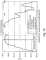
- Figure 6 shows a distribution of Br by the magnet 8a (mag. 1) on the outer peripheral surface (sleeve surface) of the developing sleeve 8 in Embodiment 1 of such a structure.
- a reference of the angle is the horizontal position (0°) of the drum, and the rotational moving direction is the opposite to the sleeve rotational moving direction.
- a vertical broken line indicates the position (blade opposing position) where the regulating blade 9 is opposed to the outer peripheral surface of the developing sleeve 8 and is the position of 86°.
- Broken lines in the opposite sides of the broken line show 3° range of the blade opposing position in the upstream and downstream sides.
- the change of the developer feeding amount attributable to the tolerances of the magnet is 3 mg/cm ⁇ 2 which is equivalent to comparison examples 2, 3, and the half-peak width can be reduced as compared with comparison examples 2, 3. That is, according to Embodiment 2, the magnetic flux density maximum value position of the blade opposing pole is 20° downstream of the half peak center portion position, and the blade opposing position is 3° upstream of the magnetic flux density maximum value position. Therefore, even if the maximum of the blade opposing pole is shifted upstream by 3°, the change of the magnetic flux distribution adjacent to the regulating blade is gentle. As a result, even if the magnetic flux density distribution changes due to the tolerances, the change of the developer feeding amount can be suppressed.
Landscapes
- Physics & Mathematics (AREA)
- General Physics & Mathematics (AREA)
- Dry Development In Electrophotography (AREA)
- Magnetic Brush Developing In Electrophotography (AREA)
Priority Applications (2)
| Application Number | Priority Date | Filing Date | Title |
|---|---|---|---|
| EP25163453.1A EP4564101A3 (de) | 2014-05-22 | 2015-05-21 | Entwicklungsgerät |
| EP23197384.3A EP4286953B1 (de) | 2014-05-22 | 2015-05-21 | Entwicklungsvorrichtung |
Applications Claiming Priority (3)
| Application Number | Priority Date | Filing Date | Title |
|---|---|---|---|
| JP2014106209A JP6351375B2 (ja) | 2014-05-22 | 2014-05-22 | 現像装置 |
| PCT/JP2015/065327 WO2015178502A1 (ja) | 2014-05-22 | 2015-05-21 | 現像装置 |
| EP15795755.6A EP3147721B1 (de) | 2014-05-22 | 2015-05-21 | Entwicklungsvorrichtung |
Related Parent Applications (2)
| Application Number | Title | Priority Date | Filing Date |
|---|---|---|---|
| EP15795755.6A Division-Into EP3147721B1 (de) | 2014-05-22 | 2015-05-21 | Entwicklungsvorrichtung |
| EP15795755.6A Division EP3147721B1 (de) | 2014-05-22 | 2015-05-21 | Entwicklungsvorrichtung |
Related Child Applications (3)
| Application Number | Title | Priority Date | Filing Date |
|---|---|---|---|
| EP25163453.1A Division EP4564101A3 (de) | 2014-05-22 | 2015-05-21 | Entwicklungsgerät |
| EP23197384.3A Division EP4286953B1 (de) | 2014-05-22 | 2015-05-21 | Entwicklungsvorrichtung |
| EP23197384.3A Division-Into EP4286953B1 (de) | 2014-05-22 | 2015-05-21 | Entwicklungsvorrichtung |
Publications (3)
| Publication Number | Publication Date |
|---|---|
| EP3534218A1 true EP3534218A1 (de) | 2019-09-04 |
| EP3534218C0 EP3534218C0 (de) | 2023-10-25 |
| EP3534218B1 EP3534218B1 (de) | 2023-10-25 |
Family
ID=54554158
Family Applications (4)
| Application Number | Title | Priority Date | Filing Date |
|---|---|---|---|
| EP19156376.6A Active EP3534218B1 (de) | 2014-05-22 | 2015-05-21 | Entwicklungsvorrichtung |
| EP23197384.3A Active EP4286953B1 (de) | 2014-05-22 | 2015-05-21 | Entwicklungsvorrichtung |
| EP25163453.1A Pending EP4564101A3 (de) | 2014-05-22 | 2015-05-21 | Entwicklungsgerät |
| EP15795755.6A Active EP3147721B1 (de) | 2014-05-22 | 2015-05-21 | Entwicklungsvorrichtung |
Family Applications After (3)
| Application Number | Title | Priority Date | Filing Date |
|---|---|---|---|
| EP23197384.3A Active EP4286953B1 (de) | 2014-05-22 | 2015-05-21 | Entwicklungsvorrichtung |
| EP25163453.1A Pending EP4564101A3 (de) | 2014-05-22 | 2015-05-21 | Entwicklungsgerät |
| EP15795755.6A Active EP3147721B1 (de) | 2014-05-22 | 2015-05-21 | Entwicklungsvorrichtung |
Country Status (7)
| Country | Link |
|---|---|
| US (4) | US10303084B2 (de) |
| EP (4) | EP3534218B1 (de) |
| JP (1) | JP6351375B2 (de) |
| CN (2) | CN111142350B (de) |
| ES (1) | ES3031883T3 (de) |
| PL (1) | PL4286953T3 (de) |
| WO (1) | WO2015178502A1 (de) |
Cited By (1)
| Publication number | Priority date | Publication date | Assignee | Title |
|---|---|---|---|---|
| EP4286953A2 (de) | 2014-05-22 | 2023-12-06 | Canon Kabushiki Kaisha | Entwicklungsvorrichtung |
Families Citing this family (7)
| Publication number | Priority date | Publication date | Assignee | Title |
|---|---|---|---|---|
| JP6688188B2 (ja) * | 2015-10-08 | 2020-04-28 | シャープ株式会社 | 現像装置 |
| JP2017146398A (ja) | 2016-02-16 | 2017-08-24 | コニカミノルタ株式会社 | 現像装置および画像形成装置 |
| JP6938167B2 (ja) | 2016-03-08 | 2021-09-22 | キヤノン株式会社 | 画像形成装置 |
| JP2017203841A (ja) | 2016-05-10 | 2017-11-16 | キヤノン株式会社 | 現像装置及び画像形成装置 |
| JP2018146919A (ja) * | 2017-03-09 | 2018-09-20 | キヤノン株式会社 | 現像装置 |
| JP7840701B2 (ja) * | 2022-01-27 | 2026-04-06 | キヤノン株式会社 | 現像装置 |
| JP7826027B2 (ja) * | 2022-01-27 | 2026-03-09 | キヤノン株式会社 | 現像装置 |
Citations (4)
| Publication number | Priority date | Publication date | Assignee | Title |
|---|---|---|---|---|
| JP2003140463A (ja) | 2001-11-06 | 2003-05-14 | Konica Corp | 現像装置および画像形成装置 |
| US20080145107A1 (en) * | 2006-12-13 | 2008-06-19 | Yasuo Miyoshi | Developing device, process cartridge, and image forming apparatus |
| WO2013162074A1 (en) * | 2012-04-27 | 2013-10-31 | Canon Kabushiki Kaisha | Developing device |
| EP3147721A1 (de) | 2014-05-22 | 2017-03-29 | Canon Kabushiki Kaisha | Entwicklungsvorrichtung |
Family Cites Families (20)
| Publication number | Priority date | Publication date | Assignee | Title |
|---|---|---|---|---|
| US3014705A (en) | 1958-08-11 | 1961-12-26 | Fairchild Stratos Corp | Cryogenic spray ejector |
| JP2759527B2 (ja) | 1989-11-22 | 1998-05-28 | 鐘淵化学工業株式会社 | 電子写真現像法 |
| JP4132350B2 (ja) * | 1998-03-16 | 2008-08-13 | 株式会社リコー | 画像形成方法ならびに画像形成装置 |
| JP2002244440A (ja) * | 2001-02-14 | 2002-08-30 | Matsushita Electric Ind Co Ltd | 画像形成装置 |
| JP3574078B2 (ja) | 2001-03-16 | 2004-10-06 | 東京エレクトロンデバイス株式会社 | 記憶装置と記憶装置制御方法 |
| JP4422921B2 (ja) * | 2001-03-22 | 2010-03-03 | 株式会社リコー | 現像ユニットと画像形成装置 |
| JP2004219510A (ja) * | 2003-01-10 | 2004-08-05 | Ricoh Co Ltd | 現像装置、プロセスカートリッジ及び画像形成装置 |
| JP2005250013A (ja) * | 2004-03-03 | 2005-09-15 | Ricoh Co Ltd | 現像ローラ、現像装置、プロセスカートリッジ及び画像形成装置 |
| JP2005331632A (ja) * | 2004-05-19 | 2005-12-02 | Canon Finetech Inc | 現像装置およびプロセスカートリッジならびにそれらを備えた画像形成装置 |
| JP2006011030A (ja) * | 2004-06-25 | 2006-01-12 | Ricoh Printing Systems Ltd | 現像装置および画像形成装置 |
| JP5111735B2 (ja) | 2005-04-11 | 2013-01-09 | 株式会社リコー | 現像装置、プロセスカートリッジ、及び、画像形成装置 |
| US7840168B2 (en) * | 2006-06-23 | 2010-11-23 | Canon Kabushiki Kaisha | Developing apparatus |
| JP2008275719A (ja) * | 2007-04-26 | 2008-11-13 | Fuji Xerox Co Ltd | 現像装置、像保持体ユニットおよび画像形成装置 |
| JP5689219B2 (ja) | 2007-12-26 | 2015-03-25 | 株式会社リコー | 現像装置、プロセスカートリッジ及び画像形成装置 |
| JP4600529B2 (ja) * | 2008-06-17 | 2010-12-15 | コニカミノルタビジネステクノロジーズ株式会社 | 現像装置及び画像形成装置 |
| JP5504942B2 (ja) * | 2010-02-09 | 2014-05-28 | 株式会社リコー | 現像装置、プロセスカートリッジ及び画像形成装置 |
| JP5585142B2 (ja) * | 2010-03-18 | 2014-09-10 | 富士ゼロックス株式会社 | 現像装置及び画像形成装置 |
| JP5505799B2 (ja) * | 2010-08-31 | 2014-05-28 | 株式会社リコー | 現像装置、並びに、これを備えたプロセスカートリッジ及び画像形成装置 |
| US9020403B2 (en) * | 2010-12-24 | 2015-04-28 | Canon Kabushiki Kaisha | Developing device |
| JP6016393B2 (ja) * | 2012-03-15 | 2016-10-26 | キヤノン株式会社 | 現像装置 |
-
2014
- 2014-05-22 JP JP2014106209A patent/JP6351375B2/ja active Active
-
2015
- 2015-05-21 CN CN202010025636.7A patent/CN111142350B/zh active Active
- 2015-05-21 EP EP19156376.6A patent/EP3534218B1/de active Active
- 2015-05-21 ES ES23197384T patent/ES3031883T3/es active Active
- 2015-05-21 PL PL23197384.3T patent/PL4286953T3/pl unknown
- 2015-05-21 EP EP23197384.3A patent/EP4286953B1/de active Active
- 2015-05-21 CN CN201580026428.6A patent/CN106462100B/zh active Active
- 2015-05-21 WO PCT/JP2015/065327 patent/WO2015178502A1/ja not_active Ceased
- 2015-05-21 EP EP25163453.1A patent/EP4564101A3/de active Pending
- 2015-05-21 EP EP15795755.6A patent/EP3147721B1/de active Active
-
2016
- 2016-11-10 US US15/348,147 patent/US10303084B2/en active Active
-
2019
- 2019-04-10 US US16/379,995 patent/US10705451B2/en active Active
-
2020
- 2020-06-05 US US16/893,558 patent/US11256195B2/en active Active
-
2022
- 2022-01-24 US US17/582,034 patent/US11829086B2/en active Active
Patent Citations (5)
| Publication number | Priority date | Publication date | Assignee | Title |
|---|---|---|---|---|
| JP2003140463A (ja) | 2001-11-06 | 2003-05-14 | Konica Corp | 現像装置および画像形成装置 |
| US20080145107A1 (en) * | 2006-12-13 | 2008-06-19 | Yasuo Miyoshi | Developing device, process cartridge, and image forming apparatus |
| WO2013162074A1 (en) * | 2012-04-27 | 2013-10-31 | Canon Kabushiki Kaisha | Developing device |
| JP2013231853A (ja) | 2012-04-27 | 2013-11-14 | Canon Inc | 現像装置 |
| EP3147721A1 (de) | 2014-05-22 | 2017-03-29 | Canon Kabushiki Kaisha | Entwicklungsvorrichtung |
Cited By (2)
| Publication number | Priority date | Publication date | Assignee | Title |
|---|---|---|---|---|
| EP4286953A2 (de) | 2014-05-22 | 2023-12-06 | Canon Kabushiki Kaisha | Entwicklungsvorrichtung |
| EP4564101A2 (de) | 2014-05-22 | 2025-06-04 | Canon Kabushiki Kaisha | Entwicklungsgerät |
Also Published As
| Publication number | Publication date |
|---|---|
| PL4286953T3 (pl) | 2025-09-08 |
| EP4564101A3 (de) | 2025-09-03 |
| US20200301312A1 (en) | 2020-09-24 |
| US20220146963A1 (en) | 2022-05-12 |
| US11829086B2 (en) | 2023-11-28 |
| EP3147721B1 (de) | 2021-04-21 |
| EP3147721A4 (de) | 2018-01-24 |
| CN111142350A (zh) | 2020-05-12 |
| EP4286953A2 (de) | 2023-12-06 |
| JP2015222317A (ja) | 2015-12-10 |
| US11256195B2 (en) | 2022-02-22 |
| CN111142350B (zh) | 2024-11-01 |
| CN106462100A (zh) | 2017-02-22 |
| EP4564101A2 (de) | 2025-06-04 |
| CN106462100B (zh) | 2020-01-21 |
| US10303084B2 (en) | 2019-05-28 |
| US20190235412A1 (en) | 2019-08-01 |
| EP3147721A1 (de) | 2017-03-29 |
| WO2015178502A1 (ja) | 2015-11-26 |
| US20170060023A1 (en) | 2017-03-02 |
| EP4286953C0 (de) | 2025-05-07 |
| EP3534218C0 (de) | 2023-10-25 |
| EP4286953B1 (de) | 2025-05-07 |
| EP3534218B1 (de) | 2023-10-25 |
| JP6351375B2 (ja) | 2018-07-04 |
| ES3031883T3 (en) | 2025-07-11 |
| US10705451B2 (en) | 2020-07-07 |
| EP4286953A3 (de) | 2024-04-03 |
Similar Documents
| Publication | Publication Date | Title |
|---|---|---|
| US11829086B2 (en) | Developing apparatus | |
| EP3518047B1 (de) | Entwicklungsvorrichtung | |
| US9599926B2 (en) | Developing unit | |
| US8548361B2 (en) | Developing device | |
| EP2469343B1 (de) | Entwicklungsvorrichtung | |
| US9235158B2 (en) | Developing device | |
| US9563150B2 (en) | Developing device | |
| US20230251590A1 (en) | Developing device | |
| JP7147036B2 (ja) | 現像装置 | |
| JP7379625B2 (ja) | 現像装置 | |
| JP6537676B2 (ja) | 現像装置 | |
| JP6992136B2 (ja) | 現像装置 | |
| JP2019139256A (ja) | 現像装置 | |
| JP2009020210A (ja) | 現像装置およびプロセスカートリッジおよび画像形成装置 |
Legal Events
| Date | Code | Title | Description |
|---|---|---|---|
| PUAI | Public reference made under article 153(3) epc to a published international application that has entered the european phase |
Free format text: ORIGINAL CODE: 0009012 |
|
| STAA | Information on the status of an ep patent application or granted ep patent |
Free format text: STATUS: THE APPLICATION HAS BEEN PUBLISHED |
|
| AC | Divisional application: reference to earlier application |
Ref document number: 3147721 Country of ref document: EP Kind code of ref document: P |
|
| AK | Designated contracting states |
Kind code of ref document: A1 Designated state(s): AL AT BE BG CH CY CZ DE DK EE ES FI FR GB GR HR HU IE IS IT LI LT LU LV MC MK MT NL NO PL PT RO RS SE SI SK SM TR |
|
| STAA | Information on the status of an ep patent application or granted ep patent |
Free format text: STATUS: REQUEST FOR EXAMINATION WAS MADE |
|
| 17P | Request for examination filed |
Effective date: 20200304 |
|
| RBV | Designated contracting states (corrected) |
Designated state(s): AL AT BE BG CH CY CZ DE DK EE ES FI FR GB GR HR HU IE IS IT LI LT LU LV MC MK MT NL NO PL PT RO RS SE SI SK SM TR |
|
| STAA | Information on the status of an ep patent application or granted ep patent |
Free format text: STATUS: EXAMINATION IS IN PROGRESS |
|
| 17Q | First examination report despatched |
Effective date: 20210623 |
|
| GRAP | Despatch of communication of intention to grant a patent |
Free format text: ORIGINAL CODE: EPIDOSNIGR1 |
|
| STAA | Information on the status of an ep patent application or granted ep patent |
Free format text: STATUS: GRANT OF PATENT IS INTENDED |
|
| INTG | Intention to grant announced |
Effective date: 20230512 |
|
| GRAS | Grant fee paid |
Free format text: ORIGINAL CODE: EPIDOSNIGR3 |
|
| GRAA | (expected) grant |
Free format text: ORIGINAL CODE: 0009210 |
|
| STAA | Information on the status of an ep patent application or granted ep patent |
Free format text: STATUS: THE PATENT HAS BEEN GRANTED |
|
| AC | Divisional application: reference to earlier application |
Ref document number: 3147721 Country of ref document: EP Kind code of ref document: P |
|
| AK | Designated contracting states |
Kind code of ref document: B1 Designated state(s): AL AT BE BG CH CY CZ DE DK EE ES FI FR GB GR HR HU IE IS IT LI LT LU LV MC MK MT NL NO PL PT RO RS SE SI SK SM TR |
|
| REG | Reference to a national code |
Ref country code: GB Ref legal event code: FG4D |
|
| REG | Reference to a national code |
Ref country code: CH Ref legal event code: EP |
|
| REG | Reference to a national code |
Ref country code: DE Ref legal event code: R096 Ref document number: 602015086276 Country of ref document: DE |
|
| REG | Reference to a national code |
Ref country code: IE Ref legal event code: FG4D |
|
| U01 | Request for unitary effect filed |
Effective date: 20231120 |
|
| U07 | Unitary effect registered |
Designated state(s): AT BE BG DE DK EE FI FR IT LT LU LV MT NL PT SE SI Effective date: 20231124 |
|
| PG25 | Lapsed in a contracting state [announced via postgrant information from national office to epo] |
Ref country code: GR Free format text: LAPSE BECAUSE OF FAILURE TO SUBMIT A TRANSLATION OF THE DESCRIPTION OR TO PAY THE FEE WITHIN THE PRESCRIBED TIME-LIMIT Effective date: 20240126 |
|
| PG25 | Lapsed in a contracting state [announced via postgrant information from national office to epo] |
Ref country code: IS Free format text: LAPSE BECAUSE OF FAILURE TO SUBMIT A TRANSLATION OF THE DESCRIPTION OR TO PAY THE FEE WITHIN THE PRESCRIBED TIME-LIMIT Effective date: 20240225 |
|
| PG25 | Lapsed in a contracting state [announced via postgrant information from national office to epo] |
Ref country code: ES Free format text: LAPSE BECAUSE OF FAILURE TO SUBMIT A TRANSLATION OF THE DESCRIPTION OR TO PAY THE FEE WITHIN THE PRESCRIBED TIME-LIMIT Effective date: 20231025 |
|
| PG25 | Lapsed in a contracting state [announced via postgrant information from national office to epo] |
Ref country code: IS Free format text: LAPSE BECAUSE OF FAILURE TO SUBMIT A TRANSLATION OF THE DESCRIPTION OR TO PAY THE FEE WITHIN THE PRESCRIBED TIME-LIMIT Effective date: 20240225 Ref country code: GR Free format text: LAPSE BECAUSE OF FAILURE TO SUBMIT A TRANSLATION OF THE DESCRIPTION OR TO PAY THE FEE WITHIN THE PRESCRIBED TIME-LIMIT Effective date: 20240126 Ref country code: ES Free format text: LAPSE BECAUSE OF FAILURE TO SUBMIT A TRANSLATION OF THE DESCRIPTION OR TO PAY THE FEE WITHIN THE PRESCRIBED TIME-LIMIT Effective date: 20231025 |
|
| U20 | Renewal fee for the european patent with unitary effect paid |
Year of fee payment: 10 Effective date: 20240418 |
|
| PG25 | Lapsed in a contracting state [announced via postgrant information from national office to epo] |
Ref country code: RS Free format text: LAPSE BECAUSE OF FAILURE TO SUBMIT A TRANSLATION OF THE DESCRIPTION OR TO PAY THE FEE WITHIN THE PRESCRIBED TIME-LIMIT Effective date: 20231025 Ref country code: PL Free format text: LAPSE BECAUSE OF FAILURE TO SUBMIT A TRANSLATION OF THE DESCRIPTION OR TO PAY THE FEE WITHIN THE PRESCRIBED TIME-LIMIT Effective date: 20231025 Ref country code: NO Free format text: LAPSE BECAUSE OF FAILURE TO SUBMIT A TRANSLATION OF THE DESCRIPTION OR TO PAY THE FEE WITHIN THE PRESCRIBED TIME-LIMIT Effective date: 20240125 Ref country code: HR Free format text: LAPSE BECAUSE OF FAILURE TO SUBMIT A TRANSLATION OF THE DESCRIPTION OR TO PAY THE FEE WITHIN THE PRESCRIBED TIME-LIMIT Effective date: 20231025 |
|
| PG25 | Lapsed in a contracting state [announced via postgrant information from national office to epo] |
Ref country code: CZ Free format text: LAPSE BECAUSE OF FAILURE TO SUBMIT A TRANSLATION OF THE DESCRIPTION OR TO PAY THE FEE WITHIN THE PRESCRIBED TIME-LIMIT Effective date: 20231025 |
|
| REG | Reference to a national code |
Ref country code: DE Ref legal event code: R097 Ref document number: 602015086276 Country of ref document: DE |
|
| PG25 | Lapsed in a contracting state [announced via postgrant information from national office to epo] |
Ref country code: SK Free format text: LAPSE BECAUSE OF FAILURE TO SUBMIT A TRANSLATION OF THE DESCRIPTION OR TO PAY THE FEE WITHIN THE PRESCRIBED TIME-LIMIT Effective date: 20231025 |
|
| PG25 | Lapsed in a contracting state [announced via postgrant information from national office to epo] |
Ref country code: SM Free format text: LAPSE BECAUSE OF FAILURE TO SUBMIT A TRANSLATION OF THE DESCRIPTION OR TO PAY THE FEE WITHIN THE PRESCRIBED TIME-LIMIT Effective date: 20231025 Ref country code: SK Free format text: LAPSE BECAUSE OF FAILURE TO SUBMIT A TRANSLATION OF THE DESCRIPTION OR TO PAY THE FEE WITHIN THE PRESCRIBED TIME-LIMIT Effective date: 20231025 Ref country code: RO Free format text: LAPSE BECAUSE OF FAILURE TO SUBMIT A TRANSLATION OF THE DESCRIPTION OR TO PAY THE FEE WITHIN THE PRESCRIBED TIME-LIMIT Effective date: 20231025 Ref country code: CZ Free format text: LAPSE BECAUSE OF FAILURE TO SUBMIT A TRANSLATION OF THE DESCRIPTION OR TO PAY THE FEE WITHIN THE PRESCRIBED TIME-LIMIT Effective date: 20231025 |
|
| PLBE | No opposition filed within time limit |
Free format text: ORIGINAL CODE: 0009261 |
|
| STAA | Information on the status of an ep patent application or granted ep patent |
Free format text: STATUS: NO OPPOSITION FILED WITHIN TIME LIMIT |
|
| 26N | No opposition filed |
Effective date: 20240726 |
|
| REG | Reference to a national code |
Ref country code: CH Ref legal event code: PL |
|
| PG25 | Lapsed in a contracting state [announced via postgrant information from national office to epo] |
Ref country code: MC Free format text: LAPSE BECAUSE OF FAILURE TO SUBMIT A TRANSLATION OF THE DESCRIPTION OR TO PAY THE FEE WITHIN THE PRESCRIBED TIME-LIMIT Effective date: 20231025 |
|
| PG25 | Lapsed in a contracting state [announced via postgrant information from national office to epo] |
Ref country code: MC Free format text: LAPSE BECAUSE OF FAILURE TO SUBMIT A TRANSLATION OF THE DESCRIPTION OR TO PAY THE FEE WITHIN THE PRESCRIBED TIME-LIMIT Effective date: 20231025 Ref country code: CH Free format text: LAPSE BECAUSE OF NON-PAYMENT OF DUE FEES Effective date: 20240531 |
|
| PG25 | Lapsed in a contracting state [announced via postgrant information from national office to epo] |
Ref country code: IE Free format text: LAPSE BECAUSE OF NON-PAYMENT OF DUE FEES Effective date: 20240521 |
|
| U20 | Renewal fee for the european patent with unitary effect paid |
Year of fee payment: 11 Effective date: 20250423 |
|
| PG25 | Lapsed in a contracting state [announced via postgrant information from national office to epo] |
Ref country code: CY Free format text: LAPSE BECAUSE OF FAILURE TO SUBMIT A TRANSLATION OF THE DESCRIPTION OR TO PAY THE FEE WITHIN THE PRESCRIBED TIME-LIMIT; INVALID AB INITIO Effective date: 20150521 |
|
| PG25 | Lapsed in a contracting state [announced via postgrant information from national office to epo] |
Ref country code: HU Free format text: LAPSE BECAUSE OF FAILURE TO SUBMIT A TRANSLATION OF THE DESCRIPTION OR TO PAY THE FEE WITHIN THE PRESCRIBED TIME-LIMIT; INVALID AB INITIO Effective date: 20150521 |
|
| PGFP | Annual fee paid to national office [announced via postgrant information from national office to epo] |
Ref country code: GB Payment date: 20260317 Year of fee payment: 12 |