EP3535162B1 - Elektromagnetische abschirmung für rückspiegelanordnung - Google Patents
Elektromagnetische abschirmung für rückspiegelanordnung Download PDFInfo
- Publication number
- EP3535162B1 EP3535162B1 EP17867384.4A EP17867384A EP3535162B1 EP 3535162 B1 EP3535162 B1 EP 3535162B1 EP 17867384 A EP17867384 A EP 17867384A EP 3535162 B1 EP3535162 B1 EP 3535162B1
- Authority
- EP
- European Patent Office
- Prior art keywords
- component
- rearview assembly
- peripheral rim
- circuit board
- electromagnetic shield
- Prior art date
- Legal status (The legal status is an assumption and is not a legal conclusion. Google has not performed a legal analysis and makes no representation as to the accuracy of the status listed.)
- Active
Links
Images



Classifications
-
- B—PERFORMING OPERATIONS; TRANSPORTING
- B60—VEHICLES IN GENERAL
- B60R—VEHICLES, VEHICLE FITTINGS, OR VEHICLE PARTS, NOT OTHERWISE PROVIDED FOR
- B60R1/00—Optical viewing arrangements; Real-time viewing arrangements for drivers or passengers using optical image capturing systems, e.g. cameras or video systems specially adapted for use in or on vehicles
- B60R1/02—Rear-view mirror arrangements
- B60R1/04—Rear-view mirror arrangements mounted inside vehicle
-
- B—PERFORMING OPERATIONS; TRANSPORTING
- B60—VEHICLES IN GENERAL
- B60R—VEHICLES, VEHICLE FITTINGS, OR VEHICLE PARTS, NOT OTHERWISE PROVIDED FOR
- B60R1/00—Optical viewing arrangements; Real-time viewing arrangements for drivers or passengers using optical image capturing systems, e.g. cameras or video systems specially adapted for use in or on vehicles
- B60R1/02—Rear-view mirror arrangements
- B60R1/08—Rear-view mirror arrangements involving special optical features, e.g. avoiding blind spots, e.g. convex mirrors; Side-by-side associations of rear-view and other mirrors
- B60R1/083—Anti-glare mirrors, e.g. "day-night" mirrors
- B60R1/088—Anti-glare mirrors, e.g. "day-night" mirrors using a cell of electrically changeable optical characteristic, e.g. liquid-crystal or electrochromic mirrors
-
- G—PHYSICS
- G02—OPTICS
- G02B—OPTICAL ELEMENTS, SYSTEMS OR APPARATUS
- G02B5/00—Optical elements other than lenses
- G02B5/08—Mirrors
-
- G—PHYSICS
- G02—OPTICS
- G02F—OPTICAL DEVICES OR ARRANGEMENTS FOR THE CONTROL OF LIGHT BY MODIFICATION OF THE OPTICAL PROPERTIES OF THE MEDIA OF THE ELEMENTS INVOLVED THEREIN; NON-LINEAR OPTICS; FREQUENCY-CHANGING OF LIGHT; OPTICAL LOGIC ELEMENTS; OPTICAL ANALOGUE/DIGITAL CONVERTERS
- G02F1/00—Devices or arrangements for the control of the intensity, colour, phase, polarisation or direction of light arriving from an independent light source, e.g. switching, gating or modulating; Non-linear optics
- G02F1/01—Devices or arrangements for the control of the intensity, colour, phase, polarisation or direction of light arriving from an independent light source, e.g. switching, gating or modulating; Non-linear optics for the control of the intensity, phase, polarisation or colour
- G02F1/15—Devices or arrangements for the control of the intensity, colour, phase, polarisation or direction of light arriving from an independent light source, e.g. switching, gating or modulating; Non-linear optics for the control of the intensity, phase, polarisation or colour based on an electrochromic effect
- G02F1/153—Constructional details
- G02F1/1533—Constructional details structural features not otherwise provided for
-
- G—PHYSICS
- G02—OPTICS
- G02F—OPTICAL DEVICES OR ARRANGEMENTS FOR THE CONTROL OF LIGHT BY MODIFICATION OF THE OPTICAL PROPERTIES OF THE MEDIA OF THE ELEMENTS INVOLVED THEREIN; NON-LINEAR OPTICS; FREQUENCY-CHANGING OF LIGHT; OPTICAL LOGIC ELEMENTS; OPTICAL ANALOGUE/DIGITAL CONVERTERS
- G02F1/00—Devices or arrangements for the control of the intensity, colour, phase, polarisation or direction of light arriving from an independent light source, e.g. switching, gating or modulating; Non-linear optics
- G02F1/01—Devices or arrangements for the control of the intensity, colour, phase, polarisation or direction of light arriving from an independent light source, e.g. switching, gating or modulating; Non-linear optics for the control of the intensity, phase, polarisation or colour
- G02F1/15—Devices or arrangements for the control of the intensity, colour, phase, polarisation or direction of light arriving from an independent light source, e.g. switching, gating or modulating; Non-linear optics for the control of the intensity, phase, polarisation or colour based on an electrochromic effect
- G02F1/153—Constructional details
- G02F1/157—Structural association of cells with optical devices, e.g. reflectors or illuminating devices
-
- H—ELECTRICITY
- H05—ELECTRIC TECHNIQUES NOT OTHERWISE PROVIDED FOR
- H05K—PRINTED CIRCUITS; CASINGS OR CONSTRUCTIONAL DETAILS OF ELECTRIC APPARATUS; MANUFACTURE OF ASSEMBLAGES OF ELECTRICAL COMPONENTS
- H05K7/00—Constructional details common to different types of electric apparatus
- H05K7/20—Modifications to facilitate cooling, ventilating, or heating
- H05K7/2039—Modifications to facilitate cooling, ventilating, or heating characterised by the heat transfer by conduction from the heat generating element to a dissipating body
- H05K7/20436—Inner thermal coupling elements in heat dissipating housings, e.g. protrusions or depressions integrally formed in the housing
-
- H—ELECTRICITY
- H05—ELECTRIC TECHNIQUES NOT OTHERWISE PROVIDED FOR
- H05K—PRINTED CIRCUITS; CASINGS OR CONSTRUCTIONAL DETAILS OF ELECTRIC APPARATUS; MANUFACTURE OF ASSEMBLAGES OF ELECTRICAL COMPONENTS
- H05K7/00—Constructional details common to different types of electric apparatus
- H05K7/20—Modifications to facilitate cooling, ventilating, or heating
- H05K7/2039—Modifications to facilitate cooling, ventilating, or heating characterised by the heat transfer by conduction from the heat generating element to a dissipating body
- H05K7/20436—Inner thermal coupling elements in heat dissipating housings, e.g. protrusions or depressions integrally formed in the housing
- H05K7/20445—Inner thermal coupling elements in heat dissipating housings, e.g. protrusions or depressions integrally formed in the housing the coupling element being an additional piece, e.g. thermal standoff
- H05K7/20454—Inner thermal coupling elements in heat dissipating housings, e.g. protrusions or depressions integrally formed in the housing the coupling element being an additional piece, e.g. thermal standoff with a conformable or flexible structure compensating for irregularities, e.g. cushion bags, thermal paste
-
- H—ELECTRICITY
- H05—ELECTRIC TECHNIQUES NOT OTHERWISE PROVIDED FOR
- H05K—PRINTED CIRCUITS; CASINGS OR CONSTRUCTIONAL DETAILS OF ELECTRIC APPARATUS; MANUFACTURE OF ASSEMBLAGES OF ELECTRICAL COMPONENTS
- H05K9/00—Screening of apparatus or components against electric or magnetic fields
- H05K9/0007—Casings
- H05K9/002—Casings with localised screening
- H05K9/0022—Casings with localised screening of components mounted on printed circuit boards [PCB]
- H05K9/0024—Shield cases mounted on a PCB, e.g. cans or caps or conformal shields
- H05K9/0032—Shield cases mounted on a PCB, e.g. cans or caps or conformal shields having multiple parts, e.g. frames mating with lids
-
- H—ELECTRICITY
- H05—ELECTRIC TECHNIQUES NOT OTHERWISE PROVIDED FOR
- H05K—PRINTED CIRCUITS; CASINGS OR CONSTRUCTIONAL DETAILS OF ELECTRIC APPARATUS; MANUFACTURE OF ASSEMBLAGES OF ELECTRICAL COMPONENTS
- H05K9/00—Screening of apparatus or components against electric or magnetic fields
- H05K9/0073—Shielding materials
- H05K9/0081—Electromagnetic shielding materials, e.g. EMI, RFI shielding
-
- B—PERFORMING OPERATIONS; TRANSPORTING
- B60—VEHICLES IN GENERAL
- B60R—VEHICLES, VEHICLE FITTINGS, OR VEHICLE PARTS, NOT OTHERWISE PROVIDED FOR
- B60R1/00—Optical viewing arrangements; Real-time viewing arrangements for drivers or passengers using optical image capturing systems, e.g. cameras or video systems specially adapted for use in or on vehicles
- B60R1/12—Mirror assemblies combined with other articles, e.g. clocks
- B60R2001/1215—Mirror assemblies combined with other articles, e.g. clocks with information displays
-
- G—PHYSICS
- G02—OPTICS
- G02F—OPTICAL DEVICES OR ARRANGEMENTS FOR THE CONTROL OF LIGHT BY MODIFICATION OF THE OPTICAL PROPERTIES OF THE MEDIA OF THE ELEMENTS INVOLVED THEREIN; NON-LINEAR OPTICS; FREQUENCY-CHANGING OF LIGHT; OPTICAL LOGIC ELEMENTS; OPTICAL ANALOGUE/DIGITAL CONVERTERS
- G02F1/00—Devices or arrangements for the control of the intensity, colour, phase, polarisation or direction of light arriving from an independent light source, e.g. switching, gating or modulating; Non-linear optics
- G02F1/01—Devices or arrangements for the control of the intensity, colour, phase, polarisation or direction of light arriving from an independent light source, e.g. switching, gating or modulating; Non-linear optics for the control of the intensity, phase, polarisation or colour
- G02F1/15—Devices or arrangements for the control of the intensity, colour, phase, polarisation or direction of light arriving from an independent light source, e.g. switching, gating or modulating; Non-linear optics for the control of the intensity, phase, polarisation or colour based on an electrochromic effect
Definitions
- the present disclosure generally relates to a rearview assembly, and more particularly to an electromagnetic shield for a rearview assembly for a vehicle.
- a rearview assembly having a circuit board.
- a grounded heat sink is proximate the circuit board.
- a thermal pad is disposed between and in abutting contact with the circuit board and the grounded heat sink.
- An electromagnetic shield includes a first component and a second component that is separate and distinct from the first component. At least one of the first and second components includes a plurality of spring tabs disposed about a periphery thereof.
- a peripheral rim of the first and second components includes retention features. The retention features of the first component are complementary to and configured to securely engage with the retention features of the second component. The first component is configured to nest over the second component.
- the present illustrated embodiments reside primarily apparatus components related to a rearview assembly. Accordingly, the apparatus components have been represented, where appropriate, by conventional symbols in the drawings, showing only those specific details that are pertinent to understanding the embodiments of the present disclosure so as not to obscure the disclosure with details that will be readily apparent to those of ordinary skill in the art having the benefit of the description herein. Further, like numerals in the description and drawings represent like elements.
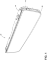
- the terms “upper,” “lower,” “right,” “left,” “rear,” “front,” “vertical,” “horizontal,” and derivatives thereof, shall relate to the disclosure as oriented in FIG. 1 .
- the term “front” shall refer to the surface of the device closer to an intended viewer of the device, and the term “rear” shall refer to the surface of the device further from the intended viewer of the device.
- the disclosure may assume various alternative orientations, except where expressly specified to the contrary.
- the specific devices and processes illustrated in the attached drawings, and described in the following specification are simply exemplary embodiments of the inventive concepts defined in the appended claims. Hence, specific dimensions and other physical characteristics relating to the embodiments disclosed herein are not to be considered as limiting, unless the claims expressly state otherwise.
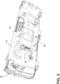
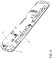
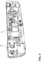
- reference numeral 10 generally designates a rearview assembly having a circuit board 12.
- a grounded heat sink 14 is proximate the circuit board 12.
- a thermal pad 16 is disposed between and in abutting contact with the circuit board 12 and the grounded heat sink 14.
- An electromagnetic shield 18 includes a plurality of spring tabs 20 disposed about a periphery 22 of the electromagnetic shield 18.
- the rearview assembly 10 as set forth herein is generally configured for use as an electro-optic assembly that includes auto dimmable features.
- the rearview assembly 10 as set forth herein may also include a full display construction such that the rearview assembly 10 provides a display of a view external to the vehicle that is captured by an imager with a field of view outside the vehicle.
- the rearview assembly 10 includes an electro-optic assembly 30 in the front portion thereof.
- the electro-optic assembly 30 may include an electrochromic construction or other similar construction.
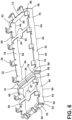
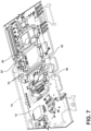
- the circuit board 12 of the rearview assembly 10 includes a variety of shielded electrical components 32 disposed proximate the electromagnetic shield 18. As shown in FIG. 6 , the electromagnetic shield 18 includes first and second components 40, 42 that are generally configured to guard against incoming or outgoing electromagnetic radiation emissions that can impact the performance of the rearview assembly 10.
- this design improves upon traditional two-piece shield designs by utilizing compliant spring fingers in the form of spring tabs 20 on the electromagnetic shield 18 to make contact with the heat sink 14, rather than using a lid.
- This allows the field programmable gate array (FPGA) chip, which is electromagnetic shielded by the compliant shield, to make improved thermal contact to the heat sink 14 via a single thermal pad 16, removing even more heat from the chip than traditional designs.
- FPGA field programmable gate array
- Traditional two-piece shields generally require two pieces of thermal tape to connect the FPGA chip to the heat sink 14, resulting in decreased thermal performance and a potentially shorter life span.
- EP1997363B1 A good example of such known construction is disclosed in EP1997363B1 , in which a combined low-profile EMI shielding and thermal management assembly is disclosed. It has a base member or frame and a lid or cover with on its inside a thermal interface in contact with a heat generating component and on the outside a thermal interface in contact with a heat sink. The heat from the heat generating component thus has to pass through three layers before it reaches the heat sink.
- U.S. Publication No. 2017/0231123 discloses pressure locking board level shield assemblies.
- U.S. Publication No. 2017/0231123 describes a board level shield (BLS) including a fence that is solderable to a printed circuit board (PCB) and a lid. When the lid is engaged to the fence that has been soldered to the PCB, the BLS provides electromagnetic interference (EMI) shielding protection to the components covered by the BLS.
- BLS board level shield
- PCB printed circuit board
- EMI electromagnetic interference
- Another know construction includes U.S. Publication No. 2002/0166683 , which discloses a push-fit shield.
- 2002/0166683 is directed to an electromagnetic interference or radio frequency interference (EMI/RFI) shield assembly for shielding PCB components, including a frame affixed to the PCB and a lid connected to the frame, which includes sidewalls that each have top and bottom portions.
- EMI/RFI electromagnetic interference or radio frequency interference
- FIG. 2007/103733 Another known construction includes International Publication No. WO 2007/103733 , which discloses combined board level shielding and thermal management for electrical components.
- International Publication No. WO 2007/103733 further discloses an apparatus that has a fence that includes walls defining at least one opening along an upper portion of the fence, a heat sink, and a thermal interface.
- the walls of the fence are configured to be disposed generally about one or more electrical components of a board.
- the heat sink includes resilient fingers connected to a lid portion, and configured to engage openings of the fence and/or the board.
- the lid portion is configured to entirely cover at least one opening of the fence for cooperatively shielding the one or more electrical components within the interior defined by the lid portion and the walls of the fence.
- the thermal interface is configured such that the engagement of the resilient fingers with the openings compresses the thermal interface between the lid portion and the one or more electrical components, thereby forming a thermally-conducting heat path from the one or more electrical components to the heat sink.
- U.S. Publication No. 2004/0052064 discloses an electromagnetic shielding and cooling device for a printed circuit board.
- U.S. Publication No. 2004/0052064 further discloses an electrically conductive contact strip arranged to form a perimeter fence.
- the contact strip used to form the shielding fence is oriented such that the contact fingers are vertical to the printed circuit board and the spring fingers face inward toward a heat producing device.
- a shielding lid which also functions as a heat sink for cooling the device, makes electrical contact around the perimeter thereof by sliding down across the contact portions of each finger of the fence, and thereby coming to rest on the heat producing device, either directly or through a thermally conductive interface.
- the first component 40 of the electromagnetic shield 18 includes a peripheral rim 50 that provides structural rigidity to the first component 40.
- the peripheral rim 50 includes four walls 52, 54, 56, 58, although additional walls may be included in the first component 40. Corners 60 of the first component 40 of the electromagnetic shield 18 generally define slots 62 that allow the walls 52, 54, 56, 58 of the peripheral rim 50 to be adjusted slightly, if desired, during installation.
- the first and second components 40, 42 also include upper lateral walls 64.
- the upper lateral walls 64 are integral with the walls 52, 54, 56, 58 of the peripheral rim 50 and can also assist in providing structural rigidity to the electromagnetic shield 18.
- the first component 40 includes a bridge 66.
- the bridge 66 extends across the first component 40 between non-adjacent walls 52, 56 and includes an enlarged central portion 67.
- the spring tabs 20 are integral with and extend from the walls 52, 54, 56, 58 of the peripheral rim 50. As previously noted, the spring tabs 20 of the electromagnetic shield 18 make contact with the heat sink and are generally compliant or compressive in structure, thereby maintaining good contact with the heat sink 14 ( FIG. 8 ).
- the walls 52, 54, 56, 58 of the peripheral rim 50 also include feet 68 indeterminately spaced about a bottom portion of the peripheral rim 50.
- the feet 68 are configured to engage the circuit board 12, and may be disposed within slots defined in the circuit board 12, or simply abut a surface of the circuit board 12.
- the spring tabs 20 face inwardly on each of the first and second components 40, 42.
- the spring tabs 20 could also face outwardly, or face inwardly and outwardly.
- the spring tabs 20 extend from only three of the four walls that define the peripheral rim 50 of the first component 40.
- additional spring tabs 20 could also be positioned on those walls that lack the spring tabs 20 to provide additional spring force on the heat sink 14.
- Application of the heat sink 14 protects and shields electrical components that are disposed on the circuit board 12. This shielding improves the performance of the electrical components, while also increasing the lifetime of these components and the rearview assembly 10 generally.
- the second component 42 includes features similar to those of the first component 40.
- a peripheral rim 70 of the second component 42 includes walls 72, 74, 76, 78.
- the walls 74, 76 are longer than the walls 72, 78.
- a bridge 80 extends across the peripheral rim 70 between the walls 74, 76.
- An upper lateral wall 82 is disposed at a top portion of the second component 42.
- the bridge 80 connects the upper lateral wall 82 disposed proximate the walls 74, 76.
- the bridge 80 includes an enlarged central portion 83.
- each of the walls 72, 74, 76, 78 includes feet 84 extending from a bottom portion of each wall 72, 74, 76, 78.
- Each corner 86 of the peripheral rim 70 defines a slot 88.
- Each of the spring tabs 20 extends upwardly from the walls 72, 74, 76, 78 of the peripheral rim 70 and provides a biasing force away from the walls 72, 74, 76, 78 of the peripheral rim 70 against the heat sink 14.
- the compliant electromagnetic shield 18 has unique spring tabs 20 disposed about the periphery 22 that make contact to ground on the circuit board 12, as well as the heat sink 14, once installed.
- the spring tab 20 spacing coupled with contact to the heat sink 14 allows the use of a single piece of thermal tape, as well as other assembly improvements. This construction solves the problem of electromagnetic shielding of the FPGA chip while at the same time improving heat transfer from the FPGA chip to the heat sink 14.
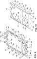
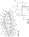
- the first component 102 includes a peripheral rim 106 defined by a plurality of walls 108, 110, 112, 114.
- the peripheral rim 106 includes upwardly extending spring tabs 120 that face inwardly and which also face outwardly.
- Each wall 108, 110, 112, 114 of the peripheral rim 106 includes a slot 122.
- the slots 122 are lined up and adjacent to the spring tabs 120.
- the peripheral rim 106 includes a plurality of retention features configured to secure the first component 102 with the second component 104, as explained in further detail herein.
- the retention features of the first component 102 include retention tabs 124 that are canted inwardly from the peripheral rim 106 of the first component 102.
- Each corner 130 of the peripheral rim 106 of the first component 102 is formed by folding adjacent walls into contact with one another.
- the first component 102 includes a bridge 132 that extends to at least three walls of the first component 102.
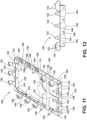
- the second component 104 of the electromagnetic shield 100 includes a peripheral rim 105 defined by a plurality of walls 140, 142, 144, 146. Corners 150 of the second component 104 define slots 152 that assist in nesting the first component 102 over the second components 104 during installation.
- the walls 140, 142, 144, 146 of the second component 104 include a plurality of retention features in the form of retention apertures 154 that are defined on the peripheral rim 105, and which are configured to receive the retention tabs 124 of the first component 102.
- the second component 104 includes a bridge 155 that extends across a central opening 156 of the second component 104, and which connects with three walls of the peripheral rim 105.
- the second component 104 includes a plurality of feet 158 configured to abut a circuit board to which the second component 104 is attached. The plurality of feet 158 may be inserted into slots defined in the circuit board, or may simply abut the circuit board.
- the first component 102 when nested, the first component 102 extends over the second component 104, substantially concealing portions of the walls of the second component 104.
- the retention features of the first component 102 are pushed slightly outward until the retention tabs 124 of the first component 102 snap-fittingly engage the retention apertures 154 of the second component 104.
- the first component 102 and the second component 104 are generally secured together.
- first component 102 and the second component 104 can be assembled prior to installation onto a printed circuit board, or the second component 104 may be installed onto the printed circuit board, and the first component 102 later positioned over the second component 104 and operably coupled with the second component 104 at that time. It will also be understood that other retention features are also possible, or that the spring tabs 120 may be disposed on the second component 104 and retention apertures may be disposed on the first component 102. In addition, it is contemplated that multiple retention features may be disposed on the peripheral rims 50, 105, or a single retention feature may be disposed on each peripheral rim 50, 105.
- the term "coupled” in all of its forms, couple, coupling, coupled, etc. generally means the joining of two components (electrical or mechanical) directly or indirectly to one another. Such joining may be stationary in nature or movable in nature. Such joining may be achieved with the two components (electrical or mechanical) and any additional intermediate members being integrally formed as a single unitary body with one another or with the two components. Such joining may be permanent in nature or may be removable or releasable in nature unless otherwise stated.
Landscapes
- Physics & Mathematics (AREA)
- Engineering & Computer Science (AREA)
- Microelectronics & Electronic Packaging (AREA)
- Nonlinear Science (AREA)
- General Physics & Mathematics (AREA)
- Optics & Photonics (AREA)
- Thermal Sciences (AREA)
- Multimedia (AREA)
- Mechanical Engineering (AREA)
- Chemical & Material Sciences (AREA)
- Crystallography & Structural Chemistry (AREA)
- Electromagnetism (AREA)
- Shielding Devices Or Components To Electric Or Magnetic Fields (AREA)
- Springs (AREA)
- Cooling Or The Like Of Electrical Apparatus (AREA)
Claims (8)
- Eine Rückblickanordnung (10), die Folgendes umfasst:eine Leiterplatte (12);einen geerdeten Kühlkörper (14) in der Nähe der Leiterplatte (12);ein Wärmeleitpad (16), das zwischen der Leiterplatte (12) und dem geerdeten Kühlkörper (14) angeordnet ist und mit diesen in Kontakt steht; undeine elektromagnetische Abschirmung (100), die Folgendes enthält: eine erste Komponente (102) und eine zweite Komponente (104), die von der ersten Komponente (102) getrennt und verschieden ist,wobei zumindest eine von der ersten Komponente (102) und der zweiten Komponente (104) eine Vielzahl von Federzungen (120) beinhaltet, die um einen Umfang davon angeordnet sind,wobei ein Umfangsrand (106, 105) der ersten und zweiten Komponente (102, 104) Rückhaltemerkmale (124, 154) beinhaltet,wobei die Rückhaltemerkmale der ersten Komponente (102) komplementär zu den Rückhaltemerkmalen der zweiten Komponente (104) sind und so konfiguriert sind, dass sie sicher in diese eingreifen,wobei die erste Komponente (102) so konfiguriert ist, dass sie nestartig über der zweiten Komponente (104) platziert werden kann (nest over).
- Die Rückblickanordnung (10) nach Anspruch 1, wobei mindestens eine von der ersten Komponente (102) und der zweiten Komponente (104) eine Brücke (132, 155) beinhaltet.
- Die Rückblickanordnung (10) nach irgendeinem der Ansprüche von 1 bis 2, wobei sowohl die erste Komponente (102) als auch die zweite Komponente (104) eine Brücke (132, 155) beinhaltet, und wobei die Brücke (132) der ersten Komponente (102) nicht mit der Brücke (155) der zweiten Komponente (104) ausgerichtet ist, wenn sich die erste Komponente (102) in einer nestartigen Position über der zweiten Komponente (104) befindet.
- Die Rückblickanordnung (10) nach irgendeinem der Ansprüche von 1 bis 3, wobei die erste Komponente (102) eine Vielzahl von sowohl nach innen als auch nach außen gerichteten Federzungen (120) beinhaltet.
- Die Rückblickanordnung (10) nach Anspruch 4, wobei mindestens eine der nach innen weisenden Federzungen (120) benachbart zu einem Spalt angeordnet ist, der im Umfangsrand (106) der ersten Komponente (102) ausgebildet ist.
- Die Rückblickanordnung (10) nach irgendeinem der Ansprüche von 1 bis 5, wobei die zweite Komponente (104) Ecken (150) beinhaltet, die Schlitze (152) definieren.
- Die Rückblickanordnung (10) nach irgendeinem der Ansprüche von 1 bis 6, wobei der Umfangsrand (106) der ersten Komponente (102) größer ist als der Umfangsrand (105) der zweiten Komponente (104).
- Die Rückblickanordnung (10) nach Anspruch 7, wobei die Brücke (132, 155) mit mindestens drei Seiten von mindestens einer der Komponenten eins und zwei (102, 104) gekoppelt ist.
Applications Claiming Priority (2)
| Application Number | Priority Date | Filing Date | Title |
|---|---|---|---|
| US201662415916P | 2016-11-01 | 2016-11-01 | |
| PCT/US2017/059496 WO2018085368A1 (en) | 2016-11-01 | 2017-11-01 | Electromagnetic shield for rearview assembly |
Publications (3)
| Publication Number | Publication Date |
|---|---|
| EP3535162A1 EP3535162A1 (de) | 2019-09-11 |
| EP3535162A4 EP3535162A4 (de) | 2019-10-02 |
| EP3535162B1 true EP3535162B1 (de) | 2023-03-22 |
Family
ID=62022149
Family Applications (1)
| Application Number | Title | Priority Date | Filing Date |
|---|---|---|---|
| EP17867384.4A Active EP3535162B1 (de) | 2016-11-01 | 2017-11-01 | Elektromagnetische abschirmung für rückspiegelanordnung |
Country Status (6)
| Country | Link |
|---|---|
| US (1) | US10342167B2 (de) |
| EP (1) | EP3535162B1 (de) |
| JP (1) | JP6679806B2 (de) |
| KR (1) | KR102414082B1 (de) |
| CN (1) | CN109890661B (de) |
| WO (1) | WO2018085368A1 (de) |
Families Citing this family (2)
| Publication number | Priority date | Publication date | Assignee | Title |
|---|---|---|---|---|
| US10893636B2 (en) * | 2017-03-10 | 2021-01-12 | Laird Technologies Inc. | Method for forming a pickup area of a board level shield |
| US11991869B2 (en) | 2022-10-11 | 2024-05-21 | Lunar Energy, Inc. | Thermal management system including an overmolded layer and a conductive layer over a circuit board |
Citations (2)
| Publication number | Priority date | Publication date | Assignee | Title |
|---|---|---|---|---|
| US20040052064A1 (en) * | 2001-11-15 | 2004-03-18 | Oliver Michael J. | Electromagnetic shielding and cooling device for printed circuit board |
| EP1997363B1 (de) * | 2006-03-09 | 2010-11-24 | Laird Technologies, Inc. | Emi-abschirmungs- und wärmemanagementbaugruppen mit rahmen und abdeckungen mit multipositionsverriegelung |
Family Cites Families (39)
| Publication number | Priority date | Publication date | Assignee | Title |
|---|---|---|---|---|
| US3338689A (en) | 1965-09-13 | 1967-08-29 | Marvin E Hetzel | Chain form clip |
| JPH0582994A (ja) * | 1991-09-20 | 1993-04-02 | Fujitsu Ltd | 箱形ユニツト構造 |
| JPH0810730B2 (ja) * | 1993-02-24 | 1996-01-31 | 日本電気株式会社 | パッケージのシールド構造 |
| US5557063A (en) | 1994-01-03 | 1996-09-17 | Lucent Technologies Inc. | Electronic component enclosure for RF shielding |
| JPH0818265A (ja) | 1994-06-29 | 1996-01-19 | Molex Inc | プリント回路基板上での電磁波等のシ−ルド方法 及びその為のシ−ルドカバ− |
| JP2793568B2 (ja) * | 1996-06-25 | 1998-09-03 | 静岡日本電気株式会社 | 電子部品の放熱構造 |
| US5717577A (en) | 1996-10-30 | 1998-02-10 | Ericsson, Inc. | Gasketed shield can for shielding emissions of electromagnetic energy |
| US6060659A (en) | 1997-07-29 | 2000-05-09 | Lucent Technologies Inc. | Electronic isolation shield and a method of determining the minimum number of securing points required on the shield to sufficiently secure the shield to a circuit board |
| US6043983A (en) * | 1998-06-17 | 2000-03-28 | Intel Corporation | EMI containment for microprocessor core mounted on a card using surface mounted clips |
| US6239359B1 (en) | 1999-05-11 | 2001-05-29 | Lucent Technologies, Inc. | Circuit board RF shielding |
| JP3270028B2 (ja) | 1999-09-10 | 2002-04-02 | 株式会社ソニー・コンピュータエンタテインメント | 電磁シールド板、電磁シールド構造体及びエンタテインメント装置 |
| JP3313682B2 (ja) * | 1999-11-18 | 2002-08-12 | 北川工業株式会社 | 電磁波シールドケース |
| JP2001148594A (ja) | 1999-11-19 | 2001-05-29 | Murata Mfg Co Ltd | シールドケース付き電子部品 |
| US6205026B1 (en) * | 2000-01-31 | 2001-03-20 | Intel Corporation | Heat sink retention components and system |
| TW477516U (en) | 2000-04-18 | 2002-02-21 | Hon Hai Prec Ind Co Ltd | Shielding structure of electronic device |
| US6552261B2 (en) * | 2001-04-27 | 2003-04-22 | Bmi, Inc. | Push-fit shield |
| US20030067757A1 (en) * | 2001-10-05 | 2003-04-10 | Richardson Patrick J. | Apparatus and method for shielding a device |
| DE10231145A1 (de) | 2002-07-10 | 2004-01-29 | Siemens Ag | Abschirmeinrichtung für elektronische Baugruppen auf einer Leiterplatte |
| US6729905B1 (en) | 2003-03-12 | 2004-05-04 | Hon Hai Precision Ind. Co., Ltd. | Transceiver cage assembly |
| US7095626B2 (en) | 2003-05-29 | 2006-08-22 | Interplex Nas Inc. | Openable one-piece electrical RF shield and method of manufacturing the same |
| US6872880B2 (en) | 2003-06-17 | 2005-03-29 | Delphi Technologies, Inc. | Two-piece solderless EMC/EMI shield |
| EP1949666B1 (de) | 2005-11-01 | 2013-07-17 | Magna Mirrors of America, Inc. | Innen-rückspiegel mit display |
| TWM289575U (en) | 2005-11-04 | 2006-04-11 | Hon Hai Prec Ind Co Ltd | Electromagnetic interference shield device |
| US7317618B2 (en) * | 2006-03-09 | 2008-01-08 | Laird Technologies, Inc. | Combined board level shielding and thermal management |
| US7422481B2 (en) * | 2006-03-22 | 2008-09-09 | Finisar Corporation | Electromagnetic interference containment in a transceiver module |
| US7351107B1 (en) | 2007-01-03 | 2008-04-01 | Delphi Technologies, Inc. | One-piece electromagnetic shield having mechanical attachment features |
| CN101578031A (zh) * | 2008-05-08 | 2009-11-11 | 莱尔德电子材料(上海)有限公司 | 屏蔽装置 |
| TWI370722B (en) * | 2008-12-22 | 2012-08-11 | Unihan Corp | Electromagnetic shielding device with heat dissipating |
| US8279624B2 (en) | 2010-06-03 | 2012-10-02 | Laird Technologies, Inc. | Board level electromagnetic interference (EMI) shields with through hole latching mechanisms |
| CN102378562A (zh) | 2010-08-19 | 2012-03-14 | 深圳富泰宏精密工业有限公司 | 电磁屏蔽罩及印刷电路板装置 |
| US8827517B2 (en) | 2010-10-12 | 2014-09-09 | Gentex Corporation | Clear bezel |
| JP2012164852A (ja) * | 2011-02-08 | 2012-08-30 | Murata Mfg Co Ltd | 半導体パッケージのシールド構造 |
| US8724342B2 (en) | 2012-03-21 | 2014-05-13 | Gentex Corporation | Shield with resilient spring snaps for removable attachment to an electrical circuit board without the use of adhesive or solder |
| US20140153192A1 (en) * | 2012-12-05 | 2014-06-05 | Molex Incorporated | Module cage with integrated emi aspect |
| JP6000170B2 (ja) * | 2013-03-15 | 2016-09-28 | 三菱電機株式会社 | 電子機器 |
| JP6403750B2 (ja) * | 2013-03-15 | 2018-10-10 | ジェンテックス コーポレイション | 表示ミラーアセンブリ |
| US9403590B2 (en) * | 2013-07-26 | 2016-08-02 | Gentex Corporation | Electro-optic window assembly EMI shield |
| US9832915B2 (en) * | 2016-02-05 | 2017-11-28 | Laird Technologies, Inc. | Pressure locking board level shield assemblies |
| DE102016213645A1 (de) | 2016-07-26 | 2018-02-01 | Robert Bosch Gmbh | Verfahren zum Betreiben einer automatisierten Feststellbremse |
-
2017
- 2017-11-01 WO PCT/US2017/059496 patent/WO2018085368A1/en not_active Ceased
- 2017-11-01 US US15/800,240 patent/US10342167B2/en active Active
- 2017-11-01 JP JP2019520372A patent/JP6679806B2/ja active Active
- 2017-11-01 CN CN201780067187.9A patent/CN109890661B/zh active Active
- 2017-11-01 KR KR1020197009723A patent/KR102414082B1/ko active Active
- 2017-11-01 EP EP17867384.4A patent/EP3535162B1/de active Active
Patent Citations (2)
| Publication number | Priority date | Publication date | Assignee | Title |
|---|---|---|---|---|
| US20040052064A1 (en) * | 2001-11-15 | 2004-03-18 | Oliver Michael J. | Electromagnetic shielding and cooling device for printed circuit board |
| EP1997363B1 (de) * | 2006-03-09 | 2010-11-24 | Laird Technologies, Inc. | Emi-abschirmungs- und wärmemanagementbaugruppen mit rahmen und abdeckungen mit multipositionsverriegelung |
Also Published As
| Publication number | Publication date |
|---|---|
| JP6679806B2 (ja) | 2020-04-15 |
| EP3535162A1 (de) | 2019-09-11 |
| KR102414082B1 (ko) | 2022-06-28 |
| CN109890661A (zh) | 2019-06-14 |
| EP3535162A4 (de) | 2019-10-02 |
| WO2018085368A1 (en) | 2018-05-11 |
| US20180124958A1 (en) | 2018-05-03 |
| CN109890661B (zh) | 2022-06-10 |
| JP2019533602A (ja) | 2019-11-21 |
| KR20190077324A (ko) | 2019-07-03 |
| US10342167B2 (en) | 2019-07-02 |
Similar Documents
| Publication | Publication Date | Title |
|---|---|---|
| EP1951021B1 (de) | Abschirmvorrichtung für elektromagnetische Interferenz und Herstellungsverfahren dafür | |
| EP2269430B1 (de) | Emi-verriegelabschirmung | |
| EP0866648B1 (de) | Zweiteilige elektromagnetische Abschirmvorrichtung zur Befestigung auf einer Leiterplatte | |
| EP2031950B1 (de) | Elektromagnetische Abschirmungen und zugehöriges Herstellungsverfahren | |
| EP3391720B1 (de) | Mehrteiliger schutzschild | |
| KR101978793B1 (ko) | 차폐 장치 | |
| US6893294B2 (en) | Transceiver cage | |
| US20040043659A1 (en) | Electrical connector having improved shielding member and method of making the same | |
| US10117367B2 (en) | Fastening structure for shield can | |
| US9832915B2 (en) | Pressure locking board level shield assemblies | |
| US20110226523A1 (en) | Electronic device | |
| US10342167B2 (en) | Electromagnetic shield for rearview assembly | |
| US8222542B2 (en) | Shielding assembly | |
| US9980418B2 (en) | RF shield assembly | |
| WO2013142549A1 (en) | Shield with resilient spring snaps for removable attachment to an electrical circuit board without the use of adhesive or solder | |
| KR101846393B1 (ko) | 튜너구조 | |
| KR20190015829A (ko) | 카메라 | |
| JP5263553B2 (ja) | シールドコネクタ | |
| CN112399768A (zh) | 屏蔽罩、电路板组件和电子设备 | |
| US20130112453A1 (en) | Structural improvement of a filter casing | |
| HK1150488B (en) | Interlocking emi shield |
Legal Events
| Date | Code | Title | Description |
|---|---|---|---|
| STAA | Information on the status of an ep patent application or granted ep patent |
Free format text: STATUS: THE INTERNATIONAL PUBLICATION HAS BEEN MADE |
|
| PUAI | Public reference made under article 153(3) epc to a published international application that has entered the european phase |
Free format text: ORIGINAL CODE: 0009012 |
|
| STAA | Information on the status of an ep patent application or granted ep patent |
Free format text: STATUS: REQUEST FOR EXAMINATION WAS MADE |
|
| 17P | Request for examination filed |
Effective date: 20190529 |
|
| AK | Designated contracting states |
Kind code of ref document: A1 Designated state(s): AL AT BE BG CH CY CZ DE DK EE ES FI FR GB GR HR HU IE IS IT LI LT LU LV MC MK MT NL NO PL PT RO RS SE SI SK SM TR |
|
| AX | Request for extension of the european patent |
Extension state: BA ME |
|
| A4 | Supplementary search report drawn up and despatched |
Effective date: 20190829 |
|
| RIC1 | Information provided on ipc code assigned before grant |
Ipc: B60R 1/04 20060101AFI20190823BHEP Ipc: B60R 1/12 20060101ALI20190823BHEP |
|
| DAV | Request for validation of the european patent (deleted) | ||
| DAX | Request for extension of the european patent (deleted) | ||
| STAA | Information on the status of an ep patent application or granted ep patent |
Free format text: STATUS: EXAMINATION IS IN PROGRESS |
|
| 17Q | First examination report despatched |
Effective date: 20200804 |
|
| REG | Reference to a national code |
Ref country code: DE Ref legal event code: R079 Ref document number: 602017067086 Country of ref document: DE Free format text: PREVIOUS MAIN CLASS: B60R0001040000 Ipc: H05K0009000000 |
|
| GRAP | Despatch of communication of intention to grant a patent |
Free format text: ORIGINAL CODE: EPIDOSNIGR1 |
|
| STAA | Information on the status of an ep patent application or granted ep patent |
Free format text: STATUS: GRANT OF PATENT IS INTENDED |
|
| RIC1 | Information provided on ipc code assigned before grant |
Ipc: B60R 1/04 20060101ALI20221031BHEP Ipc: G02B 5/08 20060101ALI20221031BHEP Ipc: G02F 1/15 20190101ALI20221031BHEP Ipc: H05K 7/20 20060101ALI20221031BHEP Ipc: H05K 9/00 20060101AFI20221031BHEP |
|
| INTG | Intention to grant announced |
Effective date: 20221115 |
|
| GRAS | Grant fee paid |
Free format text: ORIGINAL CODE: EPIDOSNIGR3 |
|
| GRAA | (expected) grant |
Free format text: ORIGINAL CODE: 0009210 |
|
| STAA | Information on the status of an ep patent application or granted ep patent |
Free format text: STATUS: THE PATENT HAS BEEN GRANTED |
|
| AK | Designated contracting states |
Kind code of ref document: B1 Designated state(s): AL AT BE BG CH CY CZ DE DK EE ES FI FR GB GR HR HU IE IS IT LI LT LU LV MC MK MT NL NO PL PT RO RS SE SI SK SM TR |
|
| REG | Reference to a national code |
Ref country code: GB Ref legal event code: FG4D |
|
| REG | Reference to a national code |
Ref country code: CH Ref legal event code: EP |
|
| REG | Reference to a national code |
Ref country code: IE Ref legal event code: FG4D |
|
| REG | Reference to a national code |
Ref country code: DE Ref legal event code: R096 Ref document number: 602017067086 Country of ref document: DE |
|
| REG | Reference to a national code |
Ref country code: AT Ref legal event code: REF Ref document number: 1556041 Country of ref document: AT Kind code of ref document: T Effective date: 20230415 |
|
| P01 | Opt-out of the competence of the unified patent court (upc) registered |
Effective date: 20230503 |
|
| REG | Reference to a national code |
Ref country code: LT Ref legal event code: MG9D |
|
| REG | Reference to a national code |
Ref country code: NL Ref legal event code: MP Effective date: 20230322 |
|
| PG25 | Lapsed in a contracting state [announced via postgrant information from national office to epo] |
Ref country code: RS Free format text: LAPSE BECAUSE OF FAILURE TO SUBMIT A TRANSLATION OF THE DESCRIPTION OR TO PAY THE FEE WITHIN THE PRESCRIBED TIME-LIMIT Effective date: 20230322 Ref country code: NO Free format text: LAPSE BECAUSE OF FAILURE TO SUBMIT A TRANSLATION OF THE DESCRIPTION OR TO PAY THE FEE WITHIN THE PRESCRIBED TIME-LIMIT Effective date: 20230622 Ref country code: LV Free format text: LAPSE BECAUSE OF FAILURE TO SUBMIT A TRANSLATION OF THE DESCRIPTION OR TO PAY THE FEE WITHIN THE PRESCRIBED TIME-LIMIT Effective date: 20230322 Ref country code: LT Free format text: LAPSE BECAUSE OF FAILURE TO SUBMIT A TRANSLATION OF THE DESCRIPTION OR TO PAY THE FEE WITHIN THE PRESCRIBED TIME-LIMIT Effective date: 20230322 Ref country code: HR Free format text: LAPSE BECAUSE OF FAILURE TO SUBMIT A TRANSLATION OF THE DESCRIPTION OR TO PAY THE FEE WITHIN THE PRESCRIBED TIME-LIMIT Effective date: 20230322 |
|
| REG | Reference to a national code |
Ref country code: AT Ref legal event code: MK05 Ref document number: 1556041 Country of ref document: AT Kind code of ref document: T Effective date: 20230322 |
|
| PG25 | Lapsed in a contracting state [announced via postgrant information from national office to epo] |
Ref country code: SE Free format text: LAPSE BECAUSE OF FAILURE TO SUBMIT A TRANSLATION OF THE DESCRIPTION OR TO PAY THE FEE WITHIN THE PRESCRIBED TIME-LIMIT Effective date: 20230322 Ref country code: NL Free format text: LAPSE BECAUSE OF FAILURE TO SUBMIT A TRANSLATION OF THE DESCRIPTION OR TO PAY THE FEE WITHIN THE PRESCRIBED TIME-LIMIT Effective date: 20230322 Ref country code: GR Free format text: LAPSE BECAUSE OF FAILURE TO SUBMIT A TRANSLATION OF THE DESCRIPTION OR TO PAY THE FEE WITHIN THE PRESCRIBED TIME-LIMIT Effective date: 20230623 Ref country code: FI Free format text: LAPSE BECAUSE OF FAILURE TO SUBMIT A TRANSLATION OF THE DESCRIPTION OR TO PAY THE FEE WITHIN THE PRESCRIBED TIME-LIMIT Effective date: 20230322 |
|
| PG25 | Lapsed in a contracting state [announced via postgrant information from national office to epo] |
Ref country code: SM Free format text: LAPSE BECAUSE OF FAILURE TO SUBMIT A TRANSLATION OF THE DESCRIPTION OR TO PAY THE FEE WITHIN THE PRESCRIBED TIME-LIMIT Effective date: 20230322 Ref country code: RO Free format text: LAPSE BECAUSE OF FAILURE TO SUBMIT A TRANSLATION OF THE DESCRIPTION OR TO PAY THE FEE WITHIN THE PRESCRIBED TIME-LIMIT Effective date: 20230322 Ref country code: PT Free format text: LAPSE BECAUSE OF FAILURE TO SUBMIT A TRANSLATION OF THE DESCRIPTION OR TO PAY THE FEE WITHIN THE PRESCRIBED TIME-LIMIT Effective date: 20230724 Ref country code: ES Free format text: LAPSE BECAUSE OF FAILURE TO SUBMIT A TRANSLATION OF THE DESCRIPTION OR TO PAY THE FEE WITHIN THE PRESCRIBED TIME-LIMIT Effective date: 20230322 Ref country code: EE Free format text: LAPSE BECAUSE OF FAILURE TO SUBMIT A TRANSLATION OF THE DESCRIPTION OR TO PAY THE FEE WITHIN THE PRESCRIBED TIME-LIMIT Effective date: 20230322 Ref country code: AT Free format text: LAPSE BECAUSE OF FAILURE TO SUBMIT A TRANSLATION OF THE DESCRIPTION OR TO PAY THE FEE WITHIN THE PRESCRIBED TIME-LIMIT Effective date: 20230322 |
|
| PG25 | Lapsed in a contracting state [announced via postgrant information from national office to epo] |
Ref country code: SK Free format text: LAPSE BECAUSE OF FAILURE TO SUBMIT A TRANSLATION OF THE DESCRIPTION OR TO PAY THE FEE WITHIN THE PRESCRIBED TIME-LIMIT Effective date: 20230322 Ref country code: PL Free format text: LAPSE BECAUSE OF FAILURE TO SUBMIT A TRANSLATION OF THE DESCRIPTION OR TO PAY THE FEE WITHIN THE PRESCRIBED TIME-LIMIT Effective date: 20230322 Ref country code: IS Free format text: LAPSE BECAUSE OF FAILURE TO SUBMIT A TRANSLATION OF THE DESCRIPTION OR TO PAY THE FEE WITHIN THE PRESCRIBED TIME-LIMIT Effective date: 20230722 |
|
| REG | Reference to a national code |
Ref country code: DE Ref legal event code: R097 Ref document number: 602017067086 Country of ref document: DE |
|
| PLBE | No opposition filed within time limit |
Free format text: ORIGINAL CODE: 0009261 |
|
| STAA | Information on the status of an ep patent application or granted ep patent |
Free format text: STATUS: NO OPPOSITION FILED WITHIN TIME LIMIT |
|
| PG25 | Lapsed in a contracting state [announced via postgrant information from national office to epo] |
Ref country code: SI Free format text: LAPSE BECAUSE OF FAILURE TO SUBMIT A TRANSLATION OF THE DESCRIPTION OR TO PAY THE FEE WITHIN THE PRESCRIBED TIME-LIMIT Effective date: 20230322 Ref country code: DK Free format text: LAPSE BECAUSE OF FAILURE TO SUBMIT A TRANSLATION OF THE DESCRIPTION OR TO PAY THE FEE WITHIN THE PRESCRIBED TIME-LIMIT Effective date: 20230322 Ref country code: CZ Free format text: LAPSE BECAUSE OF FAILURE TO SUBMIT A TRANSLATION OF THE DESCRIPTION OR TO PAY THE FEE WITHIN THE PRESCRIBED TIME-LIMIT Effective date: 20230322 |
|
| 26N | No opposition filed |
Effective date: 20240102 |
|
| PG25 | Lapsed in a contracting state [announced via postgrant information from national office to epo] |
Ref country code: IT Free format text: LAPSE BECAUSE OF FAILURE TO SUBMIT A TRANSLATION OF THE DESCRIPTION OR TO PAY THE FEE WITHIN THE PRESCRIBED TIME-LIMIT Effective date: 20230322 |
|
| REG | Reference to a national code |
Ref country code: CH Ref legal event code: PL |
|
| PG25 | Lapsed in a contracting state [announced via postgrant information from national office to epo] |
Ref country code: MC Free format text: LAPSE BECAUSE OF FAILURE TO SUBMIT A TRANSLATION OF THE DESCRIPTION OR TO PAY THE FEE WITHIN THE PRESCRIBED TIME-LIMIT Effective date: 20230322 |
|
| PG25 | Lapsed in a contracting state [announced via postgrant information from national office to epo] |
Ref country code: LU Free format text: LAPSE BECAUSE OF NON-PAYMENT OF DUE FEES Effective date: 20231101 |
|
| PG25 | Lapsed in a contracting state [announced via postgrant information from national office to epo] |
Ref country code: CH Free format text: LAPSE BECAUSE OF NON-PAYMENT OF DUE FEES Effective date: 20231130 |
|
| PG25 | Lapsed in a contracting state [announced via postgrant information from national office to epo] |
Ref country code: MC Free format text: LAPSE BECAUSE OF FAILURE TO SUBMIT A TRANSLATION OF THE DESCRIPTION OR TO PAY THE FEE WITHIN THE PRESCRIBED TIME-LIMIT Effective date: 20230322 Ref country code: LU Free format text: LAPSE BECAUSE OF NON-PAYMENT OF DUE FEES Effective date: 20231101 Ref country code: CH Free format text: LAPSE BECAUSE OF NON-PAYMENT OF DUE FEES Effective date: 20231130 |
|
| REG | Reference to a national code |
Ref country code: BE Ref legal event code: MM Effective date: 20231130 |
|
| REG | Reference to a national code |
Ref country code: IE Ref legal event code: MM4A |
|
| PG25 | Lapsed in a contracting state [announced via postgrant information from national office to epo] |
Ref country code: IE Free format text: LAPSE BECAUSE OF NON-PAYMENT OF DUE FEES Effective date: 20231101 |
|
| PG25 | Lapsed in a contracting state [announced via postgrant information from national office to epo] |
Ref country code: BE Free format text: LAPSE BECAUSE OF NON-PAYMENT OF DUE FEES Effective date: 20231130 |
|
| PG25 | Lapsed in a contracting state [announced via postgrant information from national office to epo] |
Ref country code: IE Free format text: LAPSE BECAUSE OF NON-PAYMENT OF DUE FEES Effective date: 20231101 Ref country code: BE Free format text: LAPSE BECAUSE OF NON-PAYMENT OF DUE FEES Effective date: 20231130 |
|
| PG25 | Lapsed in a contracting state [announced via postgrant information from national office to epo] |
Ref country code: BG Free format text: LAPSE BECAUSE OF FAILURE TO SUBMIT A TRANSLATION OF THE DESCRIPTION OR TO PAY THE FEE WITHIN THE PRESCRIBED TIME-LIMIT Effective date: 20230322 |
|
| PG25 | Lapsed in a contracting state [announced via postgrant information from national office to epo] |
Ref country code: BG Free format text: LAPSE BECAUSE OF FAILURE TO SUBMIT A TRANSLATION OF THE DESCRIPTION OR TO PAY THE FEE WITHIN THE PRESCRIBED TIME-LIMIT Effective date: 20230322 |
|
| PG25 | Lapsed in a contracting state [announced via postgrant information from national office to epo] |
Ref country code: CY Free format text: LAPSE BECAUSE OF FAILURE TO SUBMIT A TRANSLATION OF THE DESCRIPTION OR TO PAY THE FEE WITHIN THE PRESCRIBED TIME-LIMIT; INVALID AB INITIO Effective date: 20171101 |
|
| PG25 | Lapsed in a contracting state [announced via postgrant information from national office to epo] |
Ref country code: HU Free format text: LAPSE BECAUSE OF FAILURE TO SUBMIT A TRANSLATION OF THE DESCRIPTION OR TO PAY THE FEE WITHIN THE PRESCRIBED TIME-LIMIT; INVALID AB INITIO Effective date: 20171101 |
|
| PG25 | Lapsed in a contracting state [announced via postgrant information from national office to epo] |
Ref country code: TR Free format text: LAPSE BECAUSE OF FAILURE TO SUBMIT A TRANSLATION OF THE DESCRIPTION OR TO PAY THE FEE WITHIN THE PRESCRIBED TIME-LIMIT Effective date: 20230322 |
|
| PGFP | Annual fee paid to national office [announced via postgrant information from national office to epo] |
Ref country code: DE Payment date: 20251022 Year of fee payment: 9 |
|
| PGFP | Annual fee paid to national office [announced via postgrant information from national office to epo] |
Ref country code: GB Payment date: 20251022 Year of fee payment: 9 |
|
| PGFP | Annual fee paid to national office [announced via postgrant information from national office to epo] |
Ref country code: FR Payment date: 20251022 Year of fee payment: 9 |