EP3539121B1 - Fehlertolerante anzeige - Google Patents
Fehlertolerante anzeige Download PDFInfo
- Publication number
- EP3539121B1 EP3539121B1 EP17870564.6A EP17870564A EP3539121B1 EP 3539121 B1 EP3539121 B1 EP 3539121B1 EP 17870564 A EP17870564 A EP 17870564A EP 3539121 B1 EP3539121 B1 EP 3539121B1
- Authority
- EP
- European Patent Office
- Prior art keywords
- switch
- pixel
- driver
- select
- data driver
- Prior art date
- Legal status (The legal status is an assumption and is not a legal conclusion. Google has not performed a legal analysis and makes no representation as to the accuracy of the status listed.)
- Active
Links
Images





Classifications
-
- G—PHYSICS
- G09—EDUCATION; CRYPTOGRAPHY; DISPLAY; ADVERTISING; SEALS
- G09G—ARRANGEMENTS OR CIRCUITS FOR CONTROL OF INDICATING DEVICES USING STATIC MEANS TO PRESENT VARIABLE INFORMATION
- G09G3/00—Control arrangements or circuits, of interest only in connection with visual indicators other than cathode-ray tubes
- G09G3/20—Control arrangements or circuits, of interest only in connection with visual indicators other than cathode-ray tubes for presentation of an assembly of a number of characters, e.g. a page, by composing the assembly by combination of individual elements arranged in a matrix no fixed position being assigned to or needed to be assigned to the individual characters or partial characters
- G09G3/34—Control arrangements or circuits, of interest only in connection with visual indicators other than cathode-ray tubes for presentation of an assembly of a number of characters, e.g. a page, by composing the assembly by combination of individual elements arranged in a matrix no fixed position being assigned to or needed to be assigned to the individual characters or partial characters by control of light from an independent source
- G09G3/36—Control arrangements or circuits, of interest only in connection with visual indicators other than cathode-ray tubes for presentation of an assembly of a number of characters, e.g. a page, by composing the assembly by combination of individual elements arranged in a matrix no fixed position being assigned to or needed to be assigned to the individual characters or partial characters by control of light from an independent source using liquid crystals
- G09G3/3611—Control of matrices with row and column drivers
- G09G3/3648—Control of matrices with row and column drivers using an active matrix
-
- G—PHYSICS
- G02—OPTICS
- G02F—OPTICAL DEVICES OR ARRANGEMENTS FOR THE CONTROL OF LIGHT BY MODIFICATION OF THE OPTICAL PROPERTIES OF THE MEDIA OF THE ELEMENTS INVOLVED THEREIN; NON-LINEAR OPTICS; FREQUENCY-CHANGING OF LIGHT; OPTICAL LOGIC ELEMENTS; OPTICAL ANALOGUE/DIGITAL CONVERTERS
- G02F1/00—Devices or arrangements for the control of the intensity, colour, phase, polarisation or direction of light arriving from an independent light source, e.g. switching, gating or modulating; Non-linear optics
- G02F1/01—Devices or arrangements for the control of the intensity, colour, phase, polarisation or direction of light arriving from an independent light source, e.g. switching, gating or modulating; Non-linear optics for the control of the intensity, phase, polarisation or colour
- G02F1/13—Devices or arrangements for the control of the intensity, colour, phase, polarisation or direction of light arriving from an independent light source, e.g. switching, gating or modulating; Non-linear optics for the control of the intensity, phase, polarisation or colour based on liquid crystals, e.g. single liquid crystal display cells
- G02F1/133—Constructional arrangements; Operation of liquid crystal cells; Circuit arrangements
- G02F1/136—Liquid crystal cells structurally associated with a semi-conducting layer or substrate, e.g. cells forming part of an integrated circuit
- G02F1/1362—Active matrix addressed cells
- G02F1/1368—Active matrix addressed cells in which the switching element is a three-electrode device
-
- G—PHYSICS
- G09—EDUCATION; CRYPTOGRAPHY; DISPLAY; ADVERTISING; SEALS
- G09G—ARRANGEMENTS OR CIRCUITS FOR CONTROL OF INDICATING DEVICES USING STATIC MEANS TO PRESENT VARIABLE INFORMATION
- G09G3/00—Control arrangements or circuits, of interest only in connection with visual indicators other than cathode-ray tubes
- G09G3/006—Electronic inspection or testing of displays and display drivers, e.g. of LED or LCD displays
-
- G—PHYSICS
- G09—EDUCATION; CRYPTOGRAPHY; DISPLAY; ADVERTISING; SEALS
- G09G—ARRANGEMENTS OR CIRCUITS FOR CONTROL OF INDICATING DEVICES USING STATIC MEANS TO PRESENT VARIABLE INFORMATION
- G09G3/00—Control arrangements or circuits, of interest only in connection with visual indicators other than cathode-ray tubes
- G09G3/20—Control arrangements or circuits, of interest only in connection with visual indicators other than cathode-ray tubes for presentation of an assembly of a number of characters, e.g. a page, by composing the assembly by combination of individual elements arranged in a matrix no fixed position being assigned to or needed to be assigned to the individual characters or partial characters
- G09G3/34—Control arrangements or circuits, of interest only in connection with visual indicators other than cathode-ray tubes for presentation of an assembly of a number of characters, e.g. a page, by composing the assembly by combination of individual elements arranged in a matrix no fixed position being assigned to or needed to be assigned to the individual characters or partial characters by control of light from an independent source
- G09G3/36—Control arrangements or circuits, of interest only in connection with visual indicators other than cathode-ray tubes for presentation of an assembly of a number of characters, e.g. a page, by composing the assembly by combination of individual elements arranged in a matrix no fixed position being assigned to or needed to be assigned to the individual characters or partial characters by control of light from an independent source using liquid crystals
- G09G3/3607—Control arrangements or circuits, of interest only in connection with visual indicators other than cathode-ray tubes for presentation of an assembly of a number of characters, e.g. a page, by composing the assembly by combination of individual elements arranged in a matrix no fixed position being assigned to or needed to be assigned to the individual characters or partial characters by control of light from an independent source using liquid crystals for displaying colours or for displaying grey scales with a specific pixel layout, e.g. using sub-pixels
-
- G—PHYSICS
- G02—OPTICS
- G02F—OPTICAL DEVICES OR ARRANGEMENTS FOR THE CONTROL OF LIGHT BY MODIFICATION OF THE OPTICAL PROPERTIES OF THE MEDIA OF THE ELEMENTS INVOLVED THEREIN; NON-LINEAR OPTICS; FREQUENCY-CHANGING OF LIGHT; OPTICAL LOGIC ELEMENTS; OPTICAL ANALOGUE/DIGITAL CONVERTERS
- G02F1/00—Devices or arrangements for the control of the intensity, colour, phase, polarisation or direction of light arriving from an independent light source, e.g. switching, gating or modulating; Non-linear optics
- G02F1/01—Devices or arrangements for the control of the intensity, colour, phase, polarisation or direction of light arriving from an independent light source, e.g. switching, gating or modulating; Non-linear optics for the control of the intensity, phase, polarisation or colour
- G02F1/13—Devices or arrangements for the control of the intensity, colour, phase, polarisation or direction of light arriving from an independent light source, e.g. switching, gating or modulating; Non-linear optics for the control of the intensity, phase, polarisation or colour based on liquid crystals, e.g. single liquid crystal display cells
- G02F1/133—Constructional arrangements; Operation of liquid crystal cells; Circuit arrangements
- G02F1/136—Liquid crystal cells structurally associated with a semi-conducting layer or substrate, e.g. cells forming part of an integrated circuit
- G02F1/1362—Active matrix addressed cells
- G02F1/136204—Arrangements to prevent high voltage or static electricity failures
-
- G—PHYSICS
- G09—EDUCATION; CRYPTOGRAPHY; DISPLAY; ADVERTISING; SEALS
- G09G—ARRANGEMENTS OR CIRCUITS FOR CONTROL OF INDICATING DEVICES USING STATIC MEANS TO PRESENT VARIABLE INFORMATION
- G09G2300/00—Aspects of the constitution of display devices
- G09G2300/04—Structural and physical details of display devices
- G09G2300/0439—Pixel structures
-
- G—PHYSICS
- G09—EDUCATION; CRYPTOGRAPHY; DISPLAY; ADVERTISING; SEALS
- G09G—ARRANGEMENTS OR CIRCUITS FOR CONTROL OF INDICATING DEVICES USING STATIC MEANS TO PRESENT VARIABLE INFORMATION
- G09G2300/00—Aspects of the constitution of display devices
- G09G2300/04—Structural and physical details of display devices
- G09G2300/0439—Pixel structures
- G09G2300/0452—Details of colour pixel setup, e.g. pixel composed of a red, a blue and two green components
-
- G—PHYSICS
- G09—EDUCATION; CRYPTOGRAPHY; DISPLAY; ADVERTISING; SEALS
- G09G—ARRANGEMENTS OR CIRCUITS FOR CONTROL OF INDICATING DEVICES USING STATIC MEANS TO PRESENT VARIABLE INFORMATION
- G09G2300/00—Aspects of the constitution of display devices
- G09G2300/08—Active matrix structure, i.e. with use of active elements, inclusive of non-linear two terminal elements, in the pixels together with light emitting or modulating elements
- G09G2300/0809—Several active elements per pixel in active matrix panels
-
- G—PHYSICS
- G09—EDUCATION; CRYPTOGRAPHY; DISPLAY; ADVERTISING; SEALS
- G09G—ARRANGEMENTS OR CIRCUITS FOR CONTROL OF INDICATING DEVICES USING STATIC MEANS TO PRESENT VARIABLE INFORMATION
- G09G2320/00—Control of display operating conditions
- G09G2320/02—Improving the quality of display appearance
- G09G2320/029—Improving the quality of display appearance by monitoring one or more pixels in the display panel, e.g. by monitoring a fixed reference pixel
- G09G2320/0295—Improving the quality of display appearance by monitoring one or more pixels in the display panel, e.g. by monitoring a fixed reference pixel by monitoring each display pixel
-
- G—PHYSICS
- G09—EDUCATION; CRYPTOGRAPHY; DISPLAY; ADVERTISING; SEALS
- G09G—ARRANGEMENTS OR CIRCUITS FOR CONTROL OF INDICATING DEVICES USING STATIC MEANS TO PRESENT VARIABLE INFORMATION
- G09G2330/00—Aspects of power supply; Aspects of display protection and defect management
- G09G2330/02—Details of power systems and of start or stop of display operation
- G09G2330/021—Power management, e.g. power saving
-
- G—PHYSICS
- G09—EDUCATION; CRYPTOGRAPHY; DISPLAY; ADVERTISING; SEALS
- G09G—ARRANGEMENTS OR CIRCUITS FOR CONTROL OF INDICATING DEVICES USING STATIC MEANS TO PRESENT VARIABLE INFORMATION
- G09G2330/00—Aspects of power supply; Aspects of display protection and defect management
- G09G2330/08—Fault-tolerant or redundant circuits, or circuits in which repair of defects is prepared
-
- G—PHYSICS
- G09—EDUCATION; CRYPTOGRAPHY; DISPLAY; ADVERTISING; SEALS
- G09G—ARRANGEMENTS OR CIRCUITS FOR CONTROL OF INDICATING DEVICES USING STATIC MEANS TO PRESENT VARIABLE INFORMATION
- G09G2330/00—Aspects of power supply; Aspects of display protection and defect management
- G09G2330/10—Dealing with defective pixels
-
- G—PHYSICS
- G09—EDUCATION; CRYPTOGRAPHY; DISPLAY; ADVERTISING; SEALS
- G09G—ARRANGEMENTS OR CIRCUITS FOR CONTROL OF INDICATING DEVICES USING STATIC MEANS TO PRESENT VARIABLE INFORMATION
- G09G2330/00—Aspects of power supply; Aspects of display protection and defect management
- G09G2330/12—Test circuits or failure detection circuits included in a display system, as permanent part thereof
-
- G—PHYSICS
- G09—EDUCATION; CRYPTOGRAPHY; DISPLAY; ADVERTISING; SEALS
- G09G—ARRANGEMENTS OR CIRCUITS FOR CONTROL OF INDICATING DEVICES USING STATIC MEANS TO PRESENT VARIABLE INFORMATION
- G09G3/00—Control arrangements or circuits, of interest only in connection with visual indicators other than cathode-ray tubes
- G09G3/20—Control arrangements or circuits, of interest only in connection with visual indicators other than cathode-ray tubes for presentation of an assembly of a number of characters, e.g. a page, by composing the assembly by combination of individual elements arranged in a matrix no fixed position being assigned to or needed to be assigned to the individual characters or partial characters
- G09G3/34—Control arrangements or circuits, of interest only in connection with visual indicators other than cathode-ray tubes for presentation of an assembly of a number of characters, e.g. a page, by composing the assembly by combination of individual elements arranged in a matrix no fixed position being assigned to or needed to be assigned to the individual characters or partial characters by control of light from an independent source
- G09G3/36—Control arrangements or circuits, of interest only in connection with visual indicators other than cathode-ray tubes for presentation of an assembly of a number of characters, e.g. a page, by composing the assembly by combination of individual elements arranged in a matrix no fixed position being assigned to or needed to be assigned to the individual characters or partial characters by control of light from an independent source using liquid crystals
- G09G3/3611—Control of matrices with row and column drivers
- G09G3/3674—Details of drivers for scan electrodes
- G09G3/3677—Details of drivers for scan electrodes suitable for active matrices only
-
- G—PHYSICS
- G09—EDUCATION; CRYPTOGRAPHY; DISPLAY; ADVERTISING; SEALS
- G09G—ARRANGEMENTS OR CIRCUITS FOR CONTROL OF INDICATING DEVICES USING STATIC MEANS TO PRESENT VARIABLE INFORMATION
- G09G3/00—Control arrangements or circuits, of interest only in connection with visual indicators other than cathode-ray tubes
- G09G3/20—Control arrangements or circuits, of interest only in connection with visual indicators other than cathode-ray tubes for presentation of an assembly of a number of characters, e.g. a page, by composing the assembly by combination of individual elements arranged in a matrix no fixed position being assigned to or needed to be assigned to the individual characters or partial characters
- G09G3/34—Control arrangements or circuits, of interest only in connection with visual indicators other than cathode-ray tubes for presentation of an assembly of a number of characters, e.g. a page, by composing the assembly by combination of individual elements arranged in a matrix no fixed position being assigned to or needed to be assigned to the individual characters or partial characters by control of light from an independent source
- G09G3/36—Control arrangements or circuits, of interest only in connection with visual indicators other than cathode-ray tubes for presentation of an assembly of a number of characters, e.g. a page, by composing the assembly by combination of individual elements arranged in a matrix no fixed position being assigned to or needed to be assigned to the individual characters or partial characters by control of light from an independent source using liquid crystals
- G09G3/3611—Control of matrices with row and column drivers
- G09G3/3685—Details of drivers for data electrodes
- G09G3/3688—Details of drivers for data electrodes suitable for active matrices only
Definitions
- the disclosed technique relates to systems and methods for providing visual display, in general, and to systems and methods for redundancy in visual display, in particular.
- AMLCD Active-Matrix Liquid-Crystal Display
- Figure 1A is a schematic illustration of a conventional AMLCD display, generally referenced 10, which is known in the art.
- Figure 1B and 1C are schematic illustrations of a single electrical potential setting section, generally referenced 24A R of display 10 of Figure 1A , which is known in the art, at different states.
- Figure 1D is a schematic illustration of a specific implementation of a sub-pixel, generally referenced 22A R , of display 10 of Figure 1A , which is known in the art.
- Display 10 includes a plurality of pixels 20A, 20B, 20C and 20D.
- Each of pixels 20A, 20B, 20C and 20D includes three respective sub-pixels 22A R , 22A G , 22A R , 22B R , 22B G , 22B B , 22C R , 22C G , 22C B , 22D R , 22D G and 22D B .
- a typical display such as display 10 may contain any number of pixels, from a few thousands and up to several millions and more, and that Figure 1A , provides a mere illustration of a very small portion of a typical display.
- Each of sub-pixels 22A R , 22A G , 22A R , 22B R , 22B G , 22B B , 22C R , 22C G , 22C B , 22D R , 22D G and 22D B includes a liquid crystal section directed at a predetermined wavelength range such as Red (R), Green (G) and blue (B), a respective capacitor (not shown) and further a respective electrical potential setting section referenced 24A R , 24A G , 24A R , 24B R , 24B G , 24B B , 24C R , 24C G , 24C B , 24D R , 24D G and 24D B .
- Display 10 further includes a select driver 12 and a data driver 14.
- Select driver 12 is coupled to each of electrical potential setting sections 24A R , 24A G , 24A R , 24B R , 24B G and 24B B via select line 18 1 and further to electrical potential setting sections 24C R , 24C G , 24C B , 24D R , 24D G and 24D B via select line 18 2 .
- Data driver 14 is coupled to each electrical potential setting sections 24A R and 24C R via data line 16 1R , to each electrical potential setting sections 24A G and 24C G via data line 16 1G , to each electrical potential setting sections 24A B and 24C B via data line 16 2B , to each electrical potential setting sections 24B R and 24D R via data line 16 1R , to each electrical potential setting sections 24B G and 24D G via data line 16 2G and to each electrical potential setting sections 24B B and 24D B via data line 16 2B .
- electrical potential setting section 24A R includes a switch 30.
- Switch 30 is coupled with a capacitor 32, select line 18 1 and data line 16 1R .
- Select line 18 1 controls the state of switch 30 to be either open (as shown in Figure 1B ) or closed (as shown in Figure 1C ).
- Data line 16 1R sets to a certain potential V 1 , respective with a desired state of transmittance (e.g., transparent, opaque or various levels of semi- -transparency), for the respective LCD layer (not shown).
- capacitor 32 exhibits a potential V 0 , wherein V 0 ⁇ V 1 .
- select line 18 1 changes the state of switch 30 from open to closed, thereby coupling data line 16 1R with capacitor 32 and setting capacitor 32 to exhibit potential V 1 .
- Capacitor 32 induces this potential V 1 on to the respective LCD layer which in turn is set to the desired state of transmittance.
- switch 30 is implemented in the form of a transistor 33, having a gate electrode 36, a drain electrode 34 and a source electrode 38.
- Gate electrode 36 is coupled with select line 18 1
- source electrode 38 is coupled with data line 16 1R
- drain electrode 34 is coupled with capacitor 32 and further with LCD element R of sub-pixel 24A R .
- Select line 18 1 controls the state of the transistor 33, in time to alternately be in either an open state, a closed/conductive state, a resistive state (i.e., partially/semi-conductive) and the like, coupling between date line 18 1 and capacitor 32.
- Electrical potential setting section 44 includes two switches 40 A and 40 B . Each one of switches 40 A and 40 B is coupled with a capacitor 42, and further with LCD element R of a sub-pixel (not shown), a select line 48 and to a data line 46. Select line 48 operates switches 40 A and 40 B to simultaneously be in the same state, which is either an open state or a closed state. Data line 46 simultaneously sets a potential level V 1 at one end of switches 40 A and 40 B . Once select line 48 sets switches 40 A and 40 B to the closed state, 40 A and 40 B connect data line 48 to capacitor 42, thereby charging capacitor 42 to potential level V 1 and setting it to that potential level.
- U.S. patent no. 8,832,748 to Bushell et al entitled “Apparatus for aircraft dual channel display” is directed to a display, which includes a pixel matrix, back light illumination and two video channels capable of displaying a video signal on the display panel.
- Each video channel includes respective column drivers, row drivers, LED drivers, timing controller, backlight controller and a power source.
- the column and row drives of each channel couples to the columns and rows in the pixel matrix, such as a liquid crystal matrix and drives electrically isolated, interleaved color groups within each pixel.
- a switch provides for selecting between the two independent video channels to display a video signal on the display.
- each pixel includes two or four color groups of subpixels each group includes a red, a green and a blue subpixel.
- Each channels drive one color group or a pair of color groups. Such a configuration may provide even distribution of active subpixels upon failure of one of the channels.
- EP patent application no. 1 335 343 A2 to Sasaki, titled "Liquid Crystal Display with Reduced Driving Voltage and Separate Driving Circuits for Positive and Negative Voltages” describes a frame inversion technique to prevent degradation of a liquid crystal display (LCD).
- the architecture separates the drive signal into two, one signal having positive polarity and the other having negative polarity.
- the positive signal and negative signal are applied to the LCD in a synchronized manner to produce a single alternating signal.
- US patent application publication no. US 2008/0007504 A1 to Kawaura et al. entitled “Liquid crystal display apparatus and testing method for liquid crystal display apparatus", is directed to a testing method for a liquid crystal display (LCD) apparatus wherein an accurate comparison can be performed for comparing the voltages between two data lines in the LCD, wherein when voltages retained in paired pixels are read out to two data lines they are compared with each other.
- the LCD apparatus includes a pixel array section including a plurality of unit pixels disposed in a matrix and each including a pixel transistor, a capacitive element connected to an output electrode of the pixel transistor and a liquid crystal cell configured to display a gradation in accordance with a voltage retained in the capacitive element.
- a first data line is connected to an input electrode of each unit pixel of a first pixel group in a unit of a pixel column from among the unit pixels of the pixel array section and a second data line is connected to an input electrode of each unit pixel of a second pixel group in a unit of a pixel column from among the unit pixels of the pixel array section.
- the LCD apparatus also includes a writing unit for writing a first measurement signal into the unit pixels of the first pixel group through the first data lines and for writing a second measurement signal into the unit pixels of the second pixel group through the second data lines, along with a voltage supply control unit for selectively supplying a predetermined DC voltage to the first and second data lines.
- the LCD apparatus further includes a data line short-circuiting unit for short-circuiting the first data lines and the second data lines after the voltage supply by the voltage supply control unit, a reading out unit for reading out the first and second measurement signals from the unit pixels of the first and second pixel groups into the first and second data lines, respectively, after the first and second data lines are short-circuited to each other by the data line short-circuiting unit.
- the LCD apparatus finally includes a testing unit for comparing the potentials at the first data lines and the potentials at the second data lines with each other after the reading out by the reading out unit and performing a test of the pixel array section based on a result of the comparison.
- US patent application publication no. US 2010/0214273 A1 to Shirouzu et al. entitled “Display device and method for controlling the same", is directed to a display device that includes an organic EL element and a capacitor.
- a driving transistor is connected to an anode of the organic EL element and passes a current to the organic EL element. The current corresponds to a voltage held in the capacitor.
- a first switch is located between the capacitor and a data line and the data line supplies the voltage to the capacitor.
- a voltage detector is connected to the data line for detecting an anode voltage applied to the organic EL element.
- a second switch is located between the anode and the data line.
- a controller turns on the first switch, causing the organic EL element to emit light, and causing the voltage detector to detect the anode voltage by turning off the first switch and turning on the second switch while the organic EL element is emitting light.
- US patent application publication no. US 2013/0120664 A1 to Bushell et al. entitled “Apparatus for aircraft dual channel display”, is directed to a cockpit display including an LCD panel having a liquid crystal matrix and an LED backlight having an array of LEDs for illuminating the liquid crystal matrix.
- the display includes first and second independent video channels, with each video channel having a row driver operably coupled to and driving the rows in the liquid crystal matrix, a column driver operably coupled to and driving the columns in the liquid crystal matrix, and an LED driver operably coupled to the array of LEDs to control the backlight to the liquid crystal matrix.
- the display also includes a switch for selecting between the first and second independent video channels to display a video signal on the LCD panel.
- a display device including a first select driver, a first data driver, a second select driver and a second data driver as well as a plurality of pixels.
- Each of the pixels includes at least one sub-pixel.
- Each of the sub-pixels includes a drivable visual segment, a first electrical potential setting section and a second electrical potential setting section.
- the drivable visual segment is operative to exhibit at least a first visible state and a second visible state and includes an electric potential retentioner selected from the group of a capacitor and a memory element.
- the first electrical potential setting section includes a first switch which couples the electric potential retentioner of the drivable visual segment with the first select driver and the first data driver.
- the first switch is operative to drive the drivable visual segment, at least from the first visible state to the second visible state.
- the second electrical potential setting section includes a second switch which couples the electric potential retentioner of the drivable visual segment with the second select driver and the second data driver.
- the second switch is operative to drive the drivable visual segment, independently from the first switch, at least from the first visible state to the second visible state.
- the display device further comprising means configured to determine if the first select driver, the first data driver, or the first electrical potential setting section is malfunctioning.
- the display device also comprising means configured to cut power from the first select driver and the first data driver, and to provide power to the second select driver and the second data driver in response to a determined malfunction. When the power is provided to the second select driver and the second data driver, the same display instructions provided to the first select driver and the first data driver are provided to the second select driver and the second data driver.
- a method for operating a display multi-operation architecture of a multi-pixel display having a first select driver, a first data driver, a second select driver and a second data driver as well as a plurality of sub-pixels.
- Each of the sub-pixels includes a first switch, a second switch, a first electrical potential setting section, a second electrical potential setting section and a respective drivable visual segment.
- the drivable visual segment is coupled between the first switch and the second switch and includes a respective electric potential retentioner selected from the group consisting of a capacitor and a memory element.
- the display multi-operation architecture couples to each one of the electric potential retentioners the first select driver and the first data driver with the respective first switch and the first electrical potential setting section.
- the display multi-operation architecture further couples to each one of the electric potential retentioners the second select driver and the second data driver with the respective second switch and the second electrical potential setting section.
- the method includes the procedures of: providing access to the electric potential retentioner respective of a selected one of the at least one of the sub-pixels, by employing the first switch respective of the selected sub-pixel, via the respective first data line and the respective first select line and providing access to the electric potential retentioner respective of the selected one of the at least one of the sub-pixels, by employing the second switch respective of the selected sub-pixel, via the respective second data line and the respective second select line.
- the method further includes the procedures of determining if the first select driver, the first data driver, or the first electrical potential setting section is malfunctioning and cutting power from the first select driver and the first data driver and providing power to the second select driver and the second data driver in response to a determined malfunction.
- the same display instructions are provided to the second select driver and the second data driver as provided to the first select driver and the first data driver.
- each sub-pixel includes a drivable visual segment (e.g., LCD layer, dynamic mirror), a potential retentioner (e.g., capacitor, a memory element), a first switch, coupled with a first select driver and a first data driver, and a second switch, coupled with a second select driver and a second data driver.
- a drivable visual segment e.g., LCD layer, dynamic mirror
- a potential retentioner e.g., capacitor, a memory element
- Each one of the switches is operative, independently of the other switch, to be operated by the respective select driver, coupled therewith.
- Each one of the switches is operative, independently of the other switch, to set the capacitor to the potential provided thereto by the respective data driver, coupled therewith.
- each full color pixel includes three independently operable sub-pixels, a red sub pixel, a green sub pixel and a blue sub pixel, otherwise known in the art as the RGB chromatic scheme.
- the disclosed technique can easily apply to any other chromatic schemes, such as:
- any one of these sub pixels can be set to a plurality of visible states, which are determined by the background illumination illuminating a given sub-pixel, the chromatic filter placed in front of it and the transparency level that the LCD layer is set to.
- setting a sub-pixel to a desired visible state is carried out by setting the respective LCD layer to a desired transparency level, which is associated and required for that desired visible state.
- Transitions between visible states can be discrete (i.e., "jumping" from one visible state to another), gradual or continuous (i.e., “soft") by setting the LCD from one level of transparency to another (e.g., by setting the respective capacitor from a potential level V 1 to a potential level V 2 all at once or by setting an intermediate level V 3 or gradually, respectively.
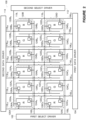
- Figure 2 is a schematic illustration of the display, generally referenced 100, constructed and operative in accordance with an embodiment of the disclosed technique.
- Display 100 includes a plurality of pixels 120A, 120B, 120C and 120D.
- Each of the pixels 120A, 120B, 120C and 120D includes three respective sub-pixels 122A R , 122A G , 122A B , 122B R , 122B G , 122B B , 122C R , 122C G , 122C B , 122D R , 122D G and 122D B .
- a typical display such as display 10, may contain any number of pixels (i.e., subject to manufacturing limitations) and further that each such pixel may include one or more sub-pixels, at any desired spectral range arrangement.
- Each of sub-pixels 122A R , 122A G , 122A B , 122B R , 122B G , 122B B , 122C R , 122C G , 122C B , 122D R , 122D G and 122D B includes a liquid crystal section directed at a predetermined wavelength range such as Red (R), Green (G) and blue (B), a respective capacitor (not shown), a first respective electrical potential setting section referenced 124A R , 124A G , 124A B , 124B R , 124B G , 124B B , 124C R , 124C G , 124C B , 124D R , 124D G , 124D B and a second respective electrical potential setting section referenced 126A R , 126A G , 126A B , 126B R , 126B G , 126B B , 126C R , 126C G , 126C
- Display 100 further includes a first select driver 102, a second select driver 112, a first data driver 104 and a second data driver 114.
- First select driver 102 is coupled to each of electrical potential setting sections 124A R , 124A G , 124A R , 124B R , 124B G and 124B B via select line 108 1 and further to electrical potential setting sections 124C R , 124C G , 124C B , 124D R , 124D G and 124D B via select line 108 2 .
- First data driver 104 is coupled to each electrical potential setting sections 124A R and 124C R via data line 106 1R , to each electrical potential setting sections 124A G and 124C G via data line 106 1G , to each electrical potential setting sections 124A B and 124C B via data line 106 1B , to each electrical potential setting sections 124B R and 124D R via data line 106 2R , to each electrical potential setting sections 124B G and 124D G via data line 106 2G and to each electrical potential setting sections 124B B and 124D B via data line 106 2B .
- Second select driver 112 is coupled to each of electrical potential setting sections 126A R , 126A G , 126A R , 126B R , 126B G and 126B B via select line 118 1 and further to electrical potential setting sections 126C R , 126C G , 126C B , 126D R , 126D G and 126D B via select line 118 2 .
- Second data driver 114 is coupled to each electrical potential setting sections 126A R and 126C R via data line 116 1R , to each electrical potential setting sections 126A G and 126C G via data line 116 1G , to each electrical potential setting sections 126A B and 126C B via data line 116 1B , to each electrical potential setting sections 126B R and 126D R via data line 116 2R , to each electrical potential setting sections 126B G and 126D G via data line 116 2G and to each electrical potential setting sections 126B B and 126D B via data line 116 2B .
- each of the above potential setting sections is associated with a respective data terminal and a respective select terminal.
- Such a respective date terminal is formed from the data line coupled with a given potential setting section and from the respective data driver coupled with that data line.
- Such a respective select terminal is formed from the select line coupled with a given potential setting section and from the respective select driver coupled with that select line.
- the select terminal of potential setting section 124A G includes select line 108 1 and select driver 102, while the data terminal of potential setting section 124A G includes data line 106 1G and data driver 104.
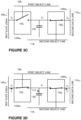
- Figure 3A is a schematic illustration of first electrical potential setting section 124A R and second electrical potential setting section 126A R , of display 100 of Figure 2 , constructed and operative in a first mode of operation, in accordance with the disclosed technique.
- Figure 3B is a schematic illustration of first electrical potential setting section 124A R and second electrical potential setting section 126A R , of display 100 of Figure 2 , constructed and operative in a second mode of operation, in accordance with the disclosed technique.
- Figure 3C is a schematic illustration of first electrical potential setting section 124A R and second electrical potential setting section 126A R , of display 100 of Figure 2 , constructed and operative in a third mode of operation, in accordance with the disclosed technique.
- Figure 3D is a schematic illustration of first electrical potential setting section 124A R and second electrical potential setting section 126A R , of display 100 of Figure 2 , constructed and operative in a fourth mode of operation, in accordance with the disclosed technique.
- first electrical potential setting section 124A R and second electrical potential setting section 126A R are both associated with sub-pixel 122A R and with a capacitor 132, which serves as an electric potential retentioner, retaining the electric potential which sets the sub-pixel 122A R LCD layer to a desired state of transmittance (e.g., transparent, opaque or various levels of semi-transparency).
- a desired state of transmittance e.g., transparent, opaque or various levels of semi-transparency
- Electrical potential setting section 124A R includes a switch 130 1 .
- Electrical potential setting section 126A R includes a switch 130 2 .
- Switch 130 1 is coupled with capacitor 132, with first select line 108 1 and with first data line 106 1R .
- Switch 130 2 is coupled with capacitor 132, with second select line 118 1 and with second data line 116 1R .
- First select line 108 1 controls the state of switch 130 1 to be either open (as shown in Figures 3A and 3C ) or closed (as shown in Figures 3B and 3D ).
- first data line 106 1R is operable to set (i.e., setting only occurs in Figures 3B and 3D )
- Capacitor 132 to a certain potential V 1 , respective with a first desired state of transmittance (e.g., transparent, opaque or various levels of semi-transparency), for the respective LCD layer (not shown).
- Second select line 118 1 controls the state of switch 130 2 to be either open (as shown in Figures 3A and 3B ) or closed (as shown in Figures 3C and 3D ).
- Data line 116 1R sets to a certain potential V 2 (in Figures 3A, 3B and 3C ), respective with a second desired state of transmittance (e.g., transparent, opaque or various levels of semi-transparency), for the respective LCD layer (not shown).
- each sub-pixel of display 100 can be driven independently, by either the first select driver 102 and first data driver 104 or second select driver 112 and second data driver 114. Accordingly, power can be toggled between the first driving electronics (i.e., first select driver 102 and first data driver 104) and the second driving electronics (i.e., second select driver 112 and second data driver 114).
- first driving electronics i.e., first select driver 102 and first data driver 104
- the second driving electronics i.e., second select driver 112 and second data driver 114.
- the electrical potential setting sections coupled therewith e.g., 124A R , 124A G , 124A R , 124B R , 124B G , 124B B , 124C R , 124C G , 124C B , 124D R , 124D G , 124D B
- power is cut off from first select driver 102 and first data driver 104 and is provided to second select driver 112 and second data
- capacitor 132 exhibits a potential V 0 , wherein V 2 ⁇ V 0 ⁇ V 1 ⁇ V 2 .
- second select line 118 1 maintains an open state for switch 130 2 while first select line 108 1 changes the state of switch 130 1 from open to closed, thereby coupling first data line 106 1R with capacitor 132 and setting capacitor 132 to exhibit potential V 1 .
- Capacitor 132 induces this potential V 1 on to the respective LCD layer which in turn is set to the first desired state of transmittance.
- first select driver 102 when, for example, one or more of first select driver 102, first data driver 104 or at least one of the electrical potential setting sections coupled therewith malfunctions, second select driver 106, second data driver 108 and the electrical potential setting sections coupled therewith are still operative to set the potential level of the capacitor respective of anyone of the sub-pixels of display 100.
- the display panel may continue to display the full image (i.e., employing all of the pixels in the display panel).
- first select line 108 1 maintains an open state for switch 130 1 while second select line 118 1 changes the state of switch 130 2 from open to closed, thereby coupling second data line 116 1R with capacitor 132 and setting capacitor 132 to exhibit potential V 2 .
- Capacitor 132 induces this potential V 2 on to the respective LCD layer which in turn is set to the second desired state of transmittance.
- switch 130 2 can set capacitor 132 to any desired potential, including V 1 (e.g., when switch 130 1 or the electronics driving it are malfunctioning)
- both data lines 106 1R and 116 1R are set to a potential V 1 .
- First select line 108 1 changes the state of switch 130 1 from open to closed thereby coupling first data line 106 1R with capacitor 132
- second select line 118 1 changes the state of switch 130 2 from open to closed, thereby coupling second data line 116 1R with capacitor 132.
- both data lines 106 1R and 116 1R are set to a potential V 1 and are hence simultaneously coupled with capacitor 132, they set capacitor 132 to exhibit potential V 1 , but typically faster than in the configuration disclosed in Figures 3B and 3C (had second data line been set to a potential V 1 ), since the current used to charge capacitor 132 is the sum of the current I 1 flowing through switch 130 1 and the current I2 flowing thought switch 130 2 (i.e., I 1 +I 2 ). It is noted that typically current I 1 is limited by the material characteristics, which the LCD TFT transistors are made of.
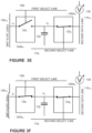
- Figures 3E and 3F are schematic illustrations of first electrical potential setting section 124A R and second electrical potential setting section 126A R , of display 100 of Figure 2 , constructed and operative in a further mode of operation, in accordance with another embodiment of the disclosed technique.
- Figures 3F is a schematic illustration of first electrical potential setting section 124A R and second electrical potential setting section 126A R , of display 100 of Figure 2 , constructed and operative in another mode of operation, in accordance with a further embodiment of the disclosed technique.
- second data line 116 1R is further coupled with a potential sensor in the form of a voltmeter 136.
- a potential sensor in the form of a voltmeter 136.
- switch 130 1 is open and switch 130 2 is closed and hence, voltmeter can measure the potential V C of capacitor 132, uninterrupted by the potential V1, which first data line 106 1R sets.
- the disclosed technique may utilize any potential measuring device, which can measure potential either directly (e.g., a voltmeter, as in the present example) or indirectly, such as by means of current meter readout integration and optionally further taking into account the characteristics of other components such as the electric potential retentioner.
- a quality measurement unit e.g., a voltmeter, an ampermeter
- first select terminal e.g., a voltmeter, an ampermeter
- second select terminal e.g., a voltmeter, an ampermeter
- Such a measurement unit can be unique for a selected line, or allocated momentarily to a plurality of lines (i.e., data lines or select lines).
- a second data line such as 116 1R can be alternatively coupled with a potential source and with a potential sensor, such when the potential sensor detects a malfunction, the potential source coupled with that second data line (i.e., together with second select line and the second switch), can serve as backup for the "first" mechanism that includes the first select line, the first data line and the first switch.
- a redundantly operable display is provided.
- the display includes a plurality of pixels, each including at least one sub-pixel.
- Each sub-pixel includes a drivable visual segment, a first switch and a second switch, the first switch being coupled with a first select driver and a first data driver and the second switch being coupled with a second select driver and a second data driver.
- first electrical potential setting section 124A R is employed to provide a first potential V 1 to the liquid crystal section R of sub-pixel 122A R .
- First potential V 1 corresponds to a desired first transparency level.
- first electrical potential setting section 124A G is employed to provide a second potential V 2 to the liquid crystal section G of sub-pixel 122A G .
- Second potential V 2 corresponds to a desired second transparency level.
- procedures 202 and 204 can be executed either in sequence or simultaneously. When executed simultaneously, procedures reduce the time required to refresh the entire display, by substantially half, since at each given moment, two sub-pixels are refreshed, instead of one. It is further noted that the method of Figure 4 , also serves in a situation wherein a certain sub-pixel can no longer be operated by its respective first electrical potential setting section, and is instead being operated by its respective second electrical potential setting section.
- a redundantly operable display is provided.
- the display includes a plurality of pixels, each including at least one sub-pixel.
- Each sub-pixel includes a drivable visual segment, a first switch and a second switch, the first switch being coupled with a first select driver and a first data driver and the second switch being coupled with a second select driver and a second data driver.
- first electrical potential setting section 126A R is employed to provide a first potential V 1 to the liquid crystal section R of sub-pixel 122A R .
- First potential V 1 corresponds to a desired first transparency level.
- the transparency state for the drivable visual segment of at least another one of the sub-pixels is set by employing the respective second switch of that sub-pixel.
- second electrical potential setting section 126A R is employed to provide a second potential V 1 to the liquid crystal section R of sub-pixel 122A R .
- Second potential V 1 also corresponds to the desired first transparency level.
- procedures 212 and 214 can be executed either in sequence or simultaneously. When executed simultaneously, procedures reduce the time required to refresh the entire display, since at each given moment, two electrical potential setting sections are used to set the desired potential for the LCD layer of a given sub-pixel, at a current which exceeds the current provided by a single electrical potential setting section, thereby reducing the time required to charge the respective capacitor of that sub-pixel.
- a display including a plurality of pixels is provided. Each of the pixels includes at least one sub-pixel. Each of the sub-pixels includes a drivable visual segment, a first switch and a second switch. The first switch is coupled with a first select driver and a second data driver. The second switch is coupled with a second select driver and a second data driver.
- display 100 includes a plurality of pixels 120A, 120B, 120C and 120D, each including sub pixels such as 122A R , 12B B and 122D G , each including a first switch (e.g., Figure 3A ) a second switch, wherein the first switches are each coupled to a first select driver 102 and a first data driver 104 and the second switches are each coupled to a second select driver 112 and a second data driver 114.
- a first switch e.g., Figure 3A
- procedure 222 access to the electric potential retentioner respective of a selected sub-pixel is provided, by employing the first switch respective of that selected sub-pixel, via the respective first data line and the respective first select line.
- access is provided to capacitor 132 by employing switch 130 1 via first select line 108 1 and first data line 106 1R .
- the access provided in procedure 222 can be provided to a variety of actions such as setting potential to the potential retentioner denoted 230, measuring the potential of the potential retentioner denoted 232 and disabling the respective switch 234.
- potential V 1 is set for capacitor 132.
- V 2 is set for capacitor 132.
- switch 130 1 can be disabled via either one of select line 108 1 and first data line 106 1R (disabling not shown).
- procedure 224 access to the electric potential retentioner respective of a selected sub-pixel is provided, by employing the second switch respective of that selected sub-pixel, via the respective second data line and the respective second select line.
- access is provided to capacitor 132 by employing switch 130 2 via first select line 118 1 and first data line 116 1R .
- the access provided in procedure 224 can be provided to a variety of actions such as setting potential to the potential retentioner, as demonstrated in the example presented in Figure 3B . Similar to procedure 222, the access provided in procedure 224 can be provided to a variety of actions such as setting potential to the potential retentioner denoted 236, measuring the potential of the potential retentioner denoted 238 and disabling the respective switch 240.
- procedure 226 access to the electric potential retentioner respective of another selected sub-pixel is provided, by employing the first switch respective of that other selected sub-pixel, via the respective first data line and the respective first select line. It is noted that since the configuration presented in Figure 3A is applied for each of the sub-pixels of display 100, the description provided in conjunction with procedure 222 can be applied with respective components (not shown) for procedure 226. Similar to procedure 222, the access provided in procedure 226 can be provided to a variety of actions such as setting potential to the potential retentioner denoted 242, measuring the potential of the potential retentioner denoted 244 and disabling the respective switch 246.
- the access provided in procedure 222, the access provided in procedure 224 and the access provided in procedure 226 can sequential or simultaneous (e.g., depending operational requirements).
Landscapes
- Engineering & Computer Science (AREA)
- Physics & Mathematics (AREA)
- General Physics & Mathematics (AREA)
- Crystallography & Structural Chemistry (AREA)
- Chemical & Material Sciences (AREA)
- Theoretical Computer Science (AREA)
- Computer Hardware Design (AREA)
- Nonlinear Science (AREA)
- Microelectronics & Electronic Packaging (AREA)
- Mathematical Physics (AREA)
- Optics & Photonics (AREA)
- Control Of Indicators Other Than Cathode Ray Tubes (AREA)
- Liquid Crystal Display Device Control (AREA)
- Liquid Crystal (AREA)
Claims (16)
- Fehlertolerante Anzeigevorrichtung, umfassend:ein erstes Auswahlansteuerelement (102);ein erstes Datenansteuerelement (104);ein zweites Auswahlansteuerelement (112);ein zweites Datenansteuerelement (114);eine Vielzahl von Pixeln (120A, 120B, 120C, 120D), wobei jedes Pixel mindestens ein Unterpixel beinhaltet;wobei jedes der Unterpixel (122AR) Folgendes umfasst:ein ansteuerbares visuelles Segment, das eine Rückhaltevorrichtung für elektrisches Potenzial umfasst, die ausgewählt ist aus der Gruppe bestehend aus: einem Kondensator (132) und einem Speicherelement, wobei das ansteuerbare visuelle Segment dazu betreibbar ist, mindestens einen ersten sichtbaren Zustand und einen zweiten sichtbaren Zustand anzunehmen; einen ersten Einstellbereich (124AR) für elektrisches Potenzial, der einen ersten Schalter (1301) umfasst, der die Rückhaltevorrichtung für elektrisches Potenzial des ansteuerbaren visuellen Segments mit dem ersten Auswahlansteuerelement (102) und dem ersten Datenansteuerelement (104) koppelt, wobei der erste Schalter (1301) dazu betreibbar ist, das ansteuerbare visuelle Segment mindestens aus dem ersten sichtbaren Zustand in den zweiten sichtbaren Zustand anzusteuern; undeinen zweiten Einstellbereich (126AR) für elektrisches Potenzial, der einen zweiten Schalter 1302) umfasst, der die Rückhaltevorrichtung für elektrisches Potenzial des ansteuerbaren visuellen Segments mit dem zweiten Auswahlansteuerelement (112) und dem zweiten Datenansteuerelement (114) koppelt, wobei der zweite Schalter (1302) des zweiten Einstellbereichs (126AR) für elektrisches Potenzial unabhängig von dem ersten Schalter (1301) dazu betreibbar ist, das ansteuerbare visuelle Segment über das zweite Auswahlansteuerelement (112) und das zweite Datenansteuerelement (114) anzusteuern, zumindest aus dem ersten sichtbaren Zustand in den zweiten sichtbaren Zustand;Mittel, die dazu konfiguriert sind, zu bestimmen, ob das erste Auswahlansteuerelement, das erste Datenansteuerelement oder der erste Einstellbereich für elektrisches Potenzial eine Fehlfunktion aufweist; undMittel, die dazu konfiguriert sind, als Reaktion auf eine bestimmte Fehlfunktion, Leistung zu dem ersten Auswahlansteuerelement und dem ersten Datenansteuerelement zu unterbrechen und dem zweiten Auswahlansteuerelement und dem zweiten Datenansteuerelement Leistung bereitzustellen,wobei, wenn die Leistung dem zweiten Auswahlansteuerelement und dem zweiten Datenansteuerelement bereitgestellt wird, dem zweiten Auswahlansteuerelement und dem zweiten Datenansteuerelement dieselben Anzeigeanweisungen bereitgestellt werden, die dem ersten Auswahlansteuerelement und dem ersten Datenansteuerelement bereitgestellt werden.
- Anzeigevorrichtung nach Anspruch 1, wobei die Rückhaltevorrichtung für elektrisches Potenzial dazu konfiguriert ist, jeweilige elektrische Potenziale zurückzuhalten, die für jeden des ersten sichtbaren Zustands und des zweiten sichtbaren Zustands erforderlich sind, wobei jedes der jeweiligen elektrischen Potenziale durch mindestens eines des ersten Einstellbereichs für elektrisches Potenzial (124AR) und des zweiten Einstellbereichs für elektrisches Potenzial (126AR) gesteuert wird.
- Anzeigevorrichtung nach Anspruch 1, wobei ein Übergang aus dem ersten sichtbaren Zustand in den zweiten sichtbaren Zustand diskret ist.
- Anzeigevorrichtung nach Anspruch 1, wobei ein Übergang aus dem ersten sichtbaren Zustand in den zweiten sichtbaren Zustand kontinuierlich ist.
- Anzeigevorrichtung nach Anspruch 2, wobei ein Übergang aus dem ersten sichtbaren Zustand in den zweiten sichtbaren Zustand über mindestens einen dritten sichtbaren Zustand, der ein elektrisches Zwischenpotenzial erfordert, ausgeführt wird.
- Anzeigevorrichtung nach Anspruch 1, ferner umfassend mindestens eine Qualitätsmesseinheit, die dazu betreibbar ist, auf mindestens eines des Folgenden zuzugreifen: a) den ersten Einstellbereich für elektrisches Potenzial (124AR) über eine erste Datenleitung (1061R), die an das erste Datenansteuerelement (104) gekoppelt ist, und über eine erste Auswahlleitung (1081), die an das erste Auswahlansteuerelement (102) gekoppelt ist, und b) den zweiten Einstellbereich für elektrisches Potenzial (126AR) über eine zweite Datenleitung (1161R), die an das zweite Datenansteuerelement (114) gekoppelt ist, und über eine zweite Auswahlleitung (1181), die an das zweite Auswahlansteuerelement (112) gekoppelt ist.
- Anzeigevorrichtung nach Anspruch 6, wobei die mindestens eine Qualitätsmesseinheit ein Potenziometer (136) ist.
- Anzeigevorrichtung nach Anspruch 6, wobei die mindestens eine Qualitätsmesseinheit ein Strommesser ist.
- Verfahren zum Betreiben einer Mehrfachbetriebanzeigearchitektur einer Mehrfachpixelanzeige, die Folgendes aufweist:ein erstes Auswahlansteuerelement (102);ein erstes Datenansteuerelement (104);ein zweites Auswahlansteuerelement (112);ein zweites Datenansteuerelement (114); undeine Vielzahl von Unterpixeln, wobei jedes Unterpixel (122AR) Folgendes umfasst:wobei das Verfahren die folgenden Prozeduren umfasst:einen ersten Schalter (1301),einen zweiten Schalter (1302),einen ersten Einstellbereich für elektrisches Potenzial (124AR),einen zweiten Einstellbereich für elektrisches Potenzial (126AR),ein ansteuerbares visuelles Segment, das zwischen dem ersten Schalter (1301) und dem zweiten Schalter (1302) gekoppelt ist, wobei das ansteuerbare visuelle Segment Folgendes umfasst: eine Rückhaltevorrichtung für elektrisches Potenzial, die ausgewählt ist aus der Gruppe bestehend aus: einem Kondensator (132) und einem Speicherelement,wobei die Mehrfachbetriebanzeigearchitektur jede der Rückhaltevorrichtungen für elektrisches Potenzial mit dem ersten Datenansteuerelement (104) und dem ersten Auswahlansteuerelement (102) über den ersten Schalter (1301) und den ersten Einstellungsbereich (124AR) für elektrisches Potenzial koppelt und ferner jede der Rückhaltevorrichtungen für elektrisches Potenzial mit dem zweiten Datenansteuerelement (114) und dem zweiten Auswahlansteuerelement (112) über den zweiten Schalter (1302) koppelt;Bereitstellen von Zugriff auf die Rückhaltevorrichtung für elektrisches Potenzial eines ausgewählten Unterpixels (122AR) der Vielzahl von Unterpixeln durch Einsetzen des ersten Schalters (1301) des ausgewählten Unterpixels (122AR) über das erste Auswahlansteuerelement (102);Bereitstellen von Zugriff auf die Rückhaltevorrichtung für elektrisches Potenzial des ausgewählten Unterpixels (122AR) der Vielzahl von Unterpixeln durch Einsetzen des zweiten Schalters (1302) des ausgewählten Unterpixels (122AR) über das zweite Auswahlansteuerelement (112);Bestimmen, ob das erste Auswahlansteuerelement, das erste Datenansteuerelement oder der erste Einstellbereich für elektrisches Potenzial eine Fehlfunktion aufweist; undals Reaktion auf das Bestimmen einer Fehlfunktion, Unterbrechen von Leistung zu dem ersten Auswahlansteuerelement und dem ersten Datenansteuerelement und Bereitstellen von Leistung an das zweite Auswahlansteuerelement und das zweite Datenansteuerelement,wobei, wenn die Leistung dem zweiten Auswahlansteuerelement und dem zweiten Datenansteuerelement bereitgestellt wird, dem zweiten Auswahlansteuerelement und dem zweiten Datenansteuerelement dieselben Anzeigeanweisungen bereitgestellt werden, die dem ersten Auswahlansteuerelement und dem ersten Datenansteuerelement bereitgestellt werden.
- Verfahren nach Anspruch 9, ferner umfassend die Prozedur des Deaktivierens des ersten Schalters (1301) des ausgewählten Unterpixels (122AR).
- Verfahren nach Anspruch 9, wobei das Einsetzen des ersten Schalters (1301) des ausgewählten Unterpixels (122AR) die Rückhaltevorrichtung für elektrisches Potenzial des ausgewählten Unterpixels (122AR) über das erste Datenansteuerelement (104) auf ein ausgewähltes Potenzialniveau einstellt.
- Verfahren nach Anspruch 9, wobei das Einsetzen des zweiten Schalters (1302) des ausgewählten Unterpixels (122AR) die Rückhaltevorrichtung für elektrisches Potenzial des ausgewählten Unterpixels (122AR) durch das zweite Datenansteuerelement (114) auf ein ausgewähltes Potenzialniveau einstellt.
- Verfahren nach Anspruch 9, wobei das Einsetzen des ersten Schalters (1301) des ausgewählten Unterpixels (122AR) Messen des Potenzialniveaus der Rückhaltevorrichtung für elektrisches Potenzial des ausgewählten Unterpixels (122AR) über den ersten Schalter (1301) umfasst.
- Verfahren nach Anspruch 9, wobei das Einsetzen des zweiten Schalters (1302) des ausgewählten Unterpixels (122AR) Messen des Potenzialniveaus der Rückhaltevorrichtung für elektrisches Potenzial jeweils von dem ausgewählten Unterpixel (122AR) über den zweiten Schalter (1302) umfasst.
- Verfahren nach Anspruch 9, ferner umfassend gleichzeitiges Durchführen der Prozeduren von 1) Zugreifen auf das ausgewählte Unterpixel (122AR) über den zweiten Schalter (1302) des ausgewählten Unterpixels (122AR) und 2) Zugreifen auf das ausgewählte Unterpixel (122AR) über den ersten Schalter (1301) des ausgewählten Unterpixels (122AR).
- Verfahren nach Anspruch 9, ferner umfassend die folgenden Prozeduren:Bereitstellen von Zugriff auf die Rückhaltevorrichtung für elektrisches Potenzial eines zweiten ausgewählten Unterpixels (122AG) durch Einsetzen des ersten Schalters (1301) des zweiten ausgewählten Unterpixels (122AG) über das erste Auswahlansteuerelement (102); undgleichzeitiges Zugreifen 3) auf das ausgewählte Unterpixel (122AR) über den zweiten Schalter (1302) des ausgewählten Unterpixels (122AR) und 4) Zugreifen auf das zweite ausgewählte Unterpixel (122AG) über den ersten Schalter (1301) des zweiten ausgewählten Unterpixels (122AG).
Applications Claiming Priority (2)
| Application Number | Priority Date | Filing Date | Title |
|---|---|---|---|
| IL248845A IL248845B (en) | 2016-11-08 | 2016-11-08 | Fault-tolerant display |
| PCT/IL2017/051205 WO2018087750A1 (en) | 2016-11-08 | 2017-11-05 | Fault tolerant display |
Publications (4)
| Publication Number | Publication Date |
|---|---|
| EP3539121A1 EP3539121A1 (de) | 2019-09-18 |
| EP3539121A4 EP3539121A4 (de) | 2020-05-20 |
| EP3539121B1 true EP3539121B1 (de) | 2025-03-19 |
| EP3539121C0 EP3539121C0 (de) | 2025-03-19 |
Family
ID=61800735
Family Applications (1)
| Application Number | Title | Priority Date | Filing Date |
|---|---|---|---|
| EP17870564.6A Active EP3539121B1 (de) | 2016-11-08 | 2017-11-05 | Fehlertolerante anzeige |
Country Status (6)
| Country | Link |
|---|---|
| US (1) | US10755658B2 (de) |
| EP (1) | EP3539121B1 (de) |
| JP (2) | JP2020502557A (de) |
| KR (1) | KR102175225B1 (de) |
| IL (1) | IL248845B (de) |
| WO (1) | WO2018087750A1 (de) |
Families Citing this family (7)
| Publication number | Priority date | Publication date | Assignee | Title |
|---|---|---|---|---|
| EP3580746A2 (de) * | 2017-02-10 | 2019-12-18 | L-3 Technologies, Inc. | Fehlertolerante lcd-anzeige mit dualen transistorpixelzellen |
| JP6841326B2 (ja) * | 2017-05-25 | 2021-03-10 | 株式会社島津製作所 | 頭部装着型表示装置 |
| US11538431B2 (en) | 2020-06-29 | 2022-12-27 | Google Llc | Larger backplane suitable for high speed applications |
| US12573349B2 (en) | 2020-06-29 | 2026-03-10 | Google Llc | Efficient image data delivery for an array of pixel memory cells |
| US11645957B1 (en) * | 2020-09-10 | 2023-05-09 | Apple Inc. | Defective display source driver screening and repair |
| US11783739B2 (en) * | 2020-09-10 | 2023-10-10 | Apple Inc. | On-chip testing architecture for display system |
| JP2025506332A (ja) * | 2022-01-05 | 2025-03-11 | グーグル エルエルシー | ピクセルドライバメモリセルのアレイのための効率的な画像データ送達 |
Family Cites Families (33)
| Publication number | Priority date | Publication date | Assignee | Title |
|---|---|---|---|---|
| JPS55159512A (en) | 1979-05-31 | 1980-12-11 | Tokyo Shibaura Electric Co | Motor driven spring actuator |
| JPS6120091A (ja) * | 1984-07-09 | 1986-01-28 | 日本電信電話株式会社 | 画像表示装置 |
| GB2206721A (en) | 1987-07-03 | 1989-01-11 | Philips Electronic Associated | Active matrix display device |
| JPH01130131A (ja) * | 1987-11-16 | 1989-05-23 | Seiko Epson Corp | ドライバー内蔵アクティブマトリクスパネル |
| US5063378A (en) | 1989-12-22 | 1991-11-05 | David Sarnoff Research Center, Inc. | Scanned liquid crystal display with select scanner redundancy |
| JPH03237434A (ja) | 1990-02-14 | 1991-10-23 | Fujitsu Ltd | アクティブマトリクスパネルとその欠陥検出方法 |
| US5151632A (en) | 1991-03-22 | 1992-09-29 | General Motors Corporation | Flat panel emissive display with redundant circuit |
| WO1994008331A1 (en) | 1992-10-06 | 1994-04-14 | Panocorp Display Systems | Drive system and method for panel displays |
| US5859627A (en) | 1992-10-19 | 1999-01-12 | Fujitsu Limited | Driving circuit for liquid-crystal display device |
| US5555001A (en) | 1994-03-08 | 1996-09-10 | Prime View Hk Limited | Redundant scheme for LCD display with integrated data driving circuit |
| US5977961A (en) | 1996-06-19 | 1999-11-02 | Sun Microsystems, Inc. | Method and apparatus for amplitude band enabled addressing arrayed elements |
| GB9705417D0 (en) * | 1997-03-15 | 1997-04-30 | Sharp Kk | Fault tolerant circuit arrangements |
| US6259504B1 (en) | 1997-12-22 | 2001-07-10 | Hyundai Electronics Industries Co., Ltd. | Liquid crystal display having split data lines |
| US6191830B1 (en) * | 1998-03-19 | 2001-02-20 | Philips Electronics North America Corporation | Electro-optical display having split storage capacitor structure for series capacitance |
| GB2341476A (en) | 1998-09-03 | 2000-03-15 | Sharp Kk | Variable resolution display device |
| JP4014831B2 (ja) | 2000-09-04 | 2007-11-28 | 株式会社半導体エネルギー研究所 | El表示装置及びその駆動方法 |
| US20030025658A1 (en) * | 2001-08-03 | 2003-02-06 | Philips Electronics North America Corporation | Redundant column drive circuitry for image display device |
| JP3906090B2 (ja) | 2002-02-05 | 2007-04-18 | シャープ株式会社 | 液晶表示装置 |
| US7728788B1 (en) | 2003-10-14 | 2010-06-01 | International Display Consortium | Segmented redundant display cell interface system and method |
| JP2007333823A (ja) * | 2006-06-13 | 2007-12-27 | Sony Corp | 液晶表示装置および液晶表示装置の検査方法 |
| JP5010030B2 (ja) * | 2008-07-04 | 2012-08-29 | パナソニック株式会社 | 表示装置及びその制御方法 |
| JP5206178B2 (ja) | 2008-07-09 | 2013-06-12 | ソニー株式会社 | 映像表示装置および電子機器 |
| RU2479000C2 (ru) | 2008-12-26 | 2013-04-10 | Шарп Кабусики Кайся | Жидкокристаллический дисплей |
| JP5299200B2 (ja) | 2009-09-29 | 2013-09-25 | 富士通株式会社 | パネルモジュール、駆動回路、表示装置および制御プログラム |
| US9202422B2 (en) | 2011-01-07 | 2015-12-01 | Sharp Kabushiki Kaisha | Liquid crystal display device |
| GB2496590A (en) | 2011-11-11 | 2013-05-22 | Ge Aviat Systems Ltd | Apparatus for aircraft dual channel display |
| EP2801022A1 (de) * | 2012-01-05 | 2014-11-12 | American Panel Corporation Inc. | Redundantes steuerungssystem für lcd |
| GB2501255B (en) | 2012-04-16 | 2018-04-11 | Ge Aviat Systems Ltd | Apparatus for aircraft dual channel display |
| JP6094855B2 (ja) | 2012-09-27 | 2017-03-15 | Nltテクノロジー株式会社 | 液晶表示素子、画像表示装置、画像表示装置の駆動方法、携帯機器 |
| GB2507524B (en) | 2012-11-01 | 2016-02-24 | Ge Aviat Systems Ltd | Apparatus for aircraft dual channel display |
| US10339882B2 (en) * | 2015-12-09 | 2019-07-02 | L-3 Communications Corporation | Fault-tolerant AMLCD display |
| WO2017210314A1 (en) * | 2016-05-31 | 2017-12-07 | Anthem Displays, Llc | Systems and methods for providing redundant data and power |
| US10037723B2 (en) * | 2016-09-15 | 2018-07-31 | L3 Communications Corp. | Fault-tolerant LCD display |
-
2016
- 2016-11-08 IL IL248845A patent/IL248845B/en active IP Right Grant
-
2017
- 2017-11-05 US US16/348,076 patent/US10755658B2/en active Active
- 2017-11-05 KR KR1020197016428A patent/KR102175225B1/ko active Active
- 2017-11-05 EP EP17870564.6A patent/EP3539121B1/de active Active
- 2017-11-05 WO PCT/IL2017/051205 patent/WO2018087750A1/en not_active Ceased
- 2017-11-05 JP JP2019523630A patent/JP2020502557A/ja active Pending
-
2020
- 2020-08-06 JP JP2020133816A patent/JP2020197740A/ja active Pending
Also Published As
| Publication number | Publication date |
|---|---|
| WO2018087750A1 (en) | 2018-05-17 |
| IL248845B (en) | 2018-03-29 |
| US10755658B2 (en) | 2020-08-25 |
| US20190259346A1 (en) | 2019-08-22 |
| KR20190092427A (ko) | 2019-08-07 |
| EP3539121A4 (de) | 2020-05-20 |
| KR102175225B1 (ko) | 2020-11-09 |
| EP3539121C0 (de) | 2025-03-19 |
| EP3539121A1 (de) | 2019-09-18 |
| JP2020197740A (ja) | 2020-12-10 |
| JP2020502557A (ja) | 2020-01-23 |
| IL248845A0 (en) | 2017-02-28 |
Similar Documents
| Publication | Publication Date | Title |
|---|---|---|
| US10755658B2 (en) | Fault tolerant LCD display using redundant drivers, select lines, data lines, and switches | |
| KR100614030B1 (ko) | 액정표시장치 | |
| US10416812B2 (en) | Display substrate and method for testing the same, display apparatus | |
| US9093042B2 (en) | Transparent display apparatus | |
| US8681081B2 (en) | Active matrix type display device and drive control circuit used in the same | |
| US9548323B2 (en) | Thin film transistor display panel and method of manufacturing the same | |
| US8587579B2 (en) | Array substrate and driving method thereof | |
| US9952478B2 (en) | Display device with positive polarity and negative polarity pixels and method for driving the same | |
| KR101448006B1 (ko) | 액정 표시 장치 | |
| KR102409349B1 (ko) | 표시장치 | |
| JP2011013288A (ja) | 表示装置 | |
| KR20240121526A (ko) | 데이터 구동 회로 및 이를 포함하는 표시 장치 | |
| US20070013631A1 (en) | Liquid crystal display driving methodology with improved power consumption | |
| US10078394B2 (en) | Liquid crystal display device having pixels with memories | |
| US8982027B2 (en) | LCD drive circuit and driving method for scanning at least two adjacent scan lines simultaneously | |
| KR20080089988A (ko) | 액정표시장치 및 이의 구동방법 | |
| US20080013008A1 (en) | Liquid Crystal Driving Circuit and Liquid Crystal Display Device with the Same | |
| CN109859716B (zh) | 液晶显示面板、显示装置和驱动方法 | |
| US9478183B2 (en) | Display device and display method | |
| KR20090048745A (ko) | 액정 화소, 그를 포함한 패널 및 표시 장치 | |
| KR20050045445A (ko) | 액정표시장치의 구동회로 |
Legal Events
| Date | Code | Title | Description |
|---|---|---|---|
| STAA | Information on the status of an ep patent application or granted ep patent |
Free format text: STATUS: THE INTERNATIONAL PUBLICATION HAS BEEN MADE |
|
| PUAI | Public reference made under article 153(3) epc to a published international application that has entered the european phase |
Free format text: ORIGINAL CODE: 0009012 |
|
| STAA | Information on the status of an ep patent application or granted ep patent |
Free format text: STATUS: REQUEST FOR EXAMINATION WAS MADE |
|
| 17P | Request for examination filed |
Effective date: 20190607 |
|
| AK | Designated contracting states |
Kind code of ref document: A1 Designated state(s): AL AT BE BG CH CY CZ DE DK EE ES FI FR GB GR HR HU IE IS IT LI LT LU LV MC MK MT NL NO PL PT RO RS SE SI SK SM TR |
|
| AX | Request for extension of the european patent |
Extension state: BA ME |
|
| DAV | Request for validation of the european patent (deleted) | ||
| DAX | Request for extension of the european patent (deleted) | ||
| A4 | Supplementary search report drawn up and despatched |
Effective date: 20200422 |
|
| RIC1 | Information provided on ipc code assigned before grant |
Ipc: G09G 3/22 20060101AFI20200416BHEP Ipc: G09G 3/00 20060101ALI20200416BHEP |
|
| STAA | Information on the status of an ep patent application or granted ep patent |
Free format text: STATUS: EXAMINATION IS IN PROGRESS |
|
| 17Q | First examination report despatched |
Effective date: 20211110 |
|
| GRAP | Despatch of communication of intention to grant a patent |
Free format text: ORIGINAL CODE: EPIDOSNIGR1 |
|
| STAA | Information on the status of an ep patent application or granted ep patent |
Free format text: STATUS: GRANT OF PATENT IS INTENDED |
|
| INTG | Intention to grant announced |
Effective date: 20241202 |
|
| GRAS | Grant fee paid |
Free format text: ORIGINAL CODE: EPIDOSNIGR3 |
|
| GRAA | (expected) grant |
Free format text: ORIGINAL CODE: 0009210 |
|
| STAA | Information on the status of an ep patent application or granted ep patent |
Free format text: STATUS: THE PATENT HAS BEEN GRANTED |
|
| AK | Designated contracting states |
Kind code of ref document: B1 Designated state(s): AL AT BE BG CH CY CZ DE DK EE ES FI FR GB GR HR HU IE IS IT LI LT LU LV MC MK MT NL NO PL PT RO RS SE SI SK SM TR |
|
| REG | Reference to a national code |
Ref country code: GB Ref legal event code: FG4D |
|
| REG | Reference to a national code |
Ref country code: CH Ref legal event code: EP |
|
| REG | Reference to a national code |
Ref country code: DE Ref legal event code: R096 Ref document number: 602017088459 Country of ref document: DE |
|
| REG | Reference to a national code |
Ref country code: IE Ref legal event code: FG4D |
|
| RAP4 | Party data changed (patent owner data changed or rights of a patent transferred) |
Owner name: ELBIT SYSTEMS LTD. |
|
| U01 | Request for unitary effect filed |
Effective date: 20250409 |
|
| U07 | Unitary effect registered |
Designated state(s): AT BE BG DE DK EE FI FR IT LT LU LV MT NL PT RO SE SI Effective date: 20250416 |
|
| PG25 | Lapsed in a contracting state [announced via postgrant information from national office to epo] |
Ref country code: RS Free format text: LAPSE BECAUSE OF FAILURE TO SUBMIT A TRANSLATION OF THE DESCRIPTION OR TO PAY THE FEE WITHIN THE PRESCRIBED TIME-LIMIT Effective date: 20250619 |
|
| PG25 | Lapsed in a contracting state [announced via postgrant information from national office to epo] |
Ref country code: NO Free format text: LAPSE BECAUSE OF FAILURE TO SUBMIT A TRANSLATION OF THE DESCRIPTION OR TO PAY THE FEE WITHIN THE PRESCRIBED TIME-LIMIT Effective date: 20250619 |
|
| PG25 | Lapsed in a contracting state [announced via postgrant information from national office to epo] |
Ref country code: HR Free format text: LAPSE BECAUSE OF FAILURE TO SUBMIT A TRANSLATION OF THE DESCRIPTION OR TO PAY THE FEE WITHIN THE PRESCRIBED TIME-LIMIT Effective date: 20250319 |
|
| PG25 | Lapsed in a contracting state [announced via postgrant information from national office to epo] |
Ref country code: GR Free format text: LAPSE BECAUSE OF FAILURE TO SUBMIT A TRANSLATION OF THE DESCRIPTION OR TO PAY THE FEE WITHIN THE PRESCRIBED TIME-LIMIT Effective date: 20250620 |
|
| PG25 | Lapsed in a contracting state [announced via postgrant information from national office to epo] |
Ref country code: SM Free format text: LAPSE BECAUSE OF FAILURE TO SUBMIT A TRANSLATION OF THE DESCRIPTION OR TO PAY THE FEE WITHIN THE PRESCRIBED TIME-LIMIT Effective date: 20250319 |
|
| PG25 | Lapsed in a contracting state [announced via postgrant information from national office to epo] |
Ref country code: ES Free format text: LAPSE BECAUSE OF FAILURE TO SUBMIT A TRANSLATION OF THE DESCRIPTION OR TO PAY THE FEE WITHIN THE PRESCRIBED TIME-LIMIT Effective date: 20250319 |
|
| PG25 | Lapsed in a contracting state [announced via postgrant information from national office to epo] |
Ref country code: PL Free format text: LAPSE BECAUSE OF FAILURE TO SUBMIT A TRANSLATION OF THE DESCRIPTION OR TO PAY THE FEE WITHIN THE PRESCRIBED TIME-LIMIT Effective date: 20250319 |
|
| PGFP | Annual fee paid to national office [announced via postgrant information from national office to epo] |
Ref country code: GB Payment date: 20250911 Year of fee payment: 9 |
|
| PG25 | Lapsed in a contracting state [announced via postgrant information from national office to epo] |
Ref country code: CZ Free format text: LAPSE BECAUSE OF FAILURE TO SUBMIT A TRANSLATION OF THE DESCRIPTION OR TO PAY THE FEE WITHIN THE PRESCRIBED TIME-LIMIT Effective date: 20250319 |
|
| PG25 | Lapsed in a contracting state [announced via postgrant information from national office to epo] |
Ref country code: SK Free format text: LAPSE BECAUSE OF FAILURE TO SUBMIT A TRANSLATION OF THE DESCRIPTION OR TO PAY THE FEE WITHIN THE PRESCRIBED TIME-LIMIT Effective date: 20250319 |
|
| PG25 | Lapsed in a contracting state [announced via postgrant information from national office to epo] |
Ref country code: IS Free format text: LAPSE BECAUSE OF FAILURE TO SUBMIT A TRANSLATION OF THE DESCRIPTION OR TO PAY THE FEE WITHIN THE PRESCRIBED TIME-LIMIT Effective date: 20250719 |
|
| U20 | Renewal fee for the european patent with unitary effect paid |
Year of fee payment: 9 Effective date: 20251008 |
|
| PLBE | No opposition filed within time limit |
Free format text: ORIGINAL CODE: 0009261 |
|
| STAA | Information on the status of an ep patent application or granted ep patent |
Free format text: STATUS: NO OPPOSITION FILED WITHIN TIME LIMIT |
|
| REG | Reference to a national code |
Ref country code: CH Ref legal event code: L10 Free format text: ST27 STATUS EVENT CODE: U-0-0-L10-L00 (AS PROVIDED BY THE NATIONAL OFFICE) Effective date: 20260128 |
|
| 26N | No opposition filed |
Effective date: 20251222 |
|
| U1N | Appointed representative for the unitary patent procedure changed after the registration of the unitary effect |
Representative=s name: MARKS & CLERK LLP; GB |