EP3540940A1 - Améliorations apportées ou se rapportant à une adaptation d'impédance - Google Patents
Améliorations apportées ou se rapportant à une adaptation d'impédance Download PDFInfo
- Publication number
- EP3540940A1 EP3540940A1 EP18275038.0A EP18275038A EP3540940A1 EP 3540940 A1 EP3540940 A1 EP 3540940A1 EP 18275038 A EP18275038 A EP 18275038A EP 3540940 A1 EP3540940 A1 EP 3540940A1
- Authority
- EP
- European Patent Office
- Prior art keywords
- matching circuit
- phase shifter
- stub
- receiver
- antenna
- Prior art date
- Legal status (The legal status is an assumption and is not a legal conclusion. Google has not performed a legal analysis and makes no representation as to the accuracy of the status listed.)
- Ceased
Links
Images
Classifications
-
- H—ELECTRICITY
- H03—ELECTRONIC CIRCUITRY
- H03H—IMPEDANCE NETWORKS, e.g. RESONANT CIRCUITS; RESONATORS
- H03H7/00—Multiple-port networks comprising only passive electrical elements as network components
- H03H7/38—Impedance-matching networks
- H03H7/383—Impedance-matching networks comprising distributed impedance elements together with lumped impedance elements
-
- H—ELECTRICITY
- H03—ELECTRONIC CIRCUITRY
- H03H—IMPEDANCE NETWORKS, e.g. RESONANT CIRCUITS; RESONATORS
- H03H7/00—Multiple-port networks comprising only passive electrical elements as network components
- H03H7/38—Impedance-matching networks
- H03H2007/386—Multiple band impedance matching
Definitions
- the present invention relates to circuits and associated techniques for impedance matching i.e. matching the impedance of one circuit to another circuit, with a view to maximising energy transfer between the two.
- first (source) circuit In practical electrical circuits, it is common for a first (source) circuit to have a first characteristic electrical impedance, and for this first (source) circuit to be connected to a second (sink) circuit, having a second characteristic electrical impedance. In the event that the first and second characteristic impedances are not equal, then a certain proportion of transmitted power will be reflected back from the sink circuit to the source circuit.
- the characteristic impedances match.
- a separate impedance matching circuit may provide an interface between the two circuits. Effectively the impedance matching circuit matches itself in both directions i.e. to each of the two circuits to ensure maximal transfer of power.
- Examples of situations where impedance matching is important include between a transmitter and an antenna and between an antenna and a receiver.
- a transmitter connected to an antenna it is desirable to ensure that as much energy from the transmitter is transferred to the antenna as possible. There are two reasons for this. Firstly, it is desirable to ensure that maximum energy is transmitted to ensure that a distant receiver receives sufficient energy to receive and decode the transmitted signal. Secondly, in the event of an impedance mismatch, a significant amount of energy may be reflected back into the output stage of a transceiver, (a transmitter with an associated receiver), which could damage it.
- the receiver part of a transceiver is configured to receive much smaller signal levels than those associated with the transmitter part and so ensuring that as little energy as possible is reflected back into the receiver part during a transmission cycle is important.
- the input to the receiver typically needs to receive as much energy from a transmitted signal as possible.
- an impedance matcher for use in a communication system, operable to match a transmitter or receiver, respectively, to an associated antenna, comprising a stub matching circuit and a phase shifter, whereby, in use, energy flows from a source to the phase shifter, to the stub matching circuit and to an electrical load.
- the load is the antenna in a transmit configuration and a receiver in a receive configuration.
- energy is arranged to flow from the antenna to the phase shifter, to the stub matching circuit, and to the receiver.
- energy is arranged to flow from the transmitter, to the phase shifter, to the stub matching circuit, and to the antenna.
- the stub matching circuitry comprises either a single stub matching circuit or a double stub matching circuit.
- the single or double stub matching circuit is either open or closed circuit.
- the stub matching circuit is a double stub matching circuit comprising two short circuit stubs.
- a transceiver comprising a first impedance matcher for a receive chain, and a second impedance matcher for a transmit chain.
- phase shifter controller operable to supply each phase shifter with a signal indicative of a channel.
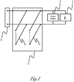
- Figure 1 shows an embodiment of the present invention. It comprises a double stub matching circuit 50, comprising a first stub 30 and a second stub 40.
- stubs are known from the prior art and can take any suitable form, depending on the form of the circuit in question and taking into account factors such as frequency of operation.
- each stub can take the form of a defined length of conductor, such as coaxial cable. The length and other characteristics (e.g. open or short circuit) can be manipulated in a known way.
- FIG. 1 i.e. a double stub with two short circuit stubs
- a double stub with two short circuit stubs is particularly useful in a marine environment, as it allows the physical location of the stub circuitry, in relation to the physical location of the antenna, to be adapted as required and can obviate the need to install the stub circuitry 50 in an awkward or inconvenient location, such as a hard-to-access compartment on a ship.
- a single stub configuration may also be used, but this offers less adaptability.
- Short circuit stubs 30, 40 are selected so that the stubs themselves do not radiate.
- a double stub matching circuit 50 is useful to match a single frequency or a relatively small range of frequencies. It is often less useful or completely unsuitable if it is required to match a relatively broad range of frequencies.
- each antenna is matched to a particular system, operating with a particular range of frequencies, some form of impedance matching may be required, which can be problematic if, as stated previously, a relatively broad range of frequencies is to be matched.
- TVWS Television White Space
- frequency spectra which have been freed up by the switching off of analogue television systems may be reutilised by other systems. This is desirable for use on marine vessels, but there is often no, or limited, free space to install a new antenna. Instead, it is often desirable to share an antenna with another on-board service or simply re-purpose an existing antenna. However, this requires impedance matching beyond the capabilities of a prior art matching circuit.
- phase shifter 20 By incorporating a phase shifter 20 between the double stub matching circuit 50 and the load 10, it is possible to manipulate the effective reflection coefficient ⁇ L( ⁇ ) of the load impedance before it arrives at the double stub matching circuit 50.
- the phase shifter affects the phase element only (or substantially), without affecting the magnitude of the reflection coefficient.
- the phase shifter 20 can be a custom-designed device or it can take the form of an off the shelf package. Suitable devices for use in embodiments of the present invention include the following devices: RFPSHT0001 D6 provided by RF Lambda; PE82P5000 provided by Pasternak; and DPS-00650155-180-8-IF-IF provided by L3 NARDA-MITEQ. Other devices may be available and these are exemplary only.
- channel m In the context of TVWS, which includes e.g. 28 frequency-spaced channels, one of the channels is selected as the basis for the double stub matching circuit 50 to operate without the need for the phase shifter 20.
- This channel is referred to as channel m. It may be considered as the base channel and is the frequency at which the double stub matcher 50 will naturally achieve optimal results.
- Channel m may be any one of the available channels.
- Other TVWS schemes in different countries may have a different number of channels.
- the phase shifter 20 is controlled by a controller such that upon a particular channel being selected for use, the phase shifter is configured to provide a phase shift associated with that channel or frequency.
- the concept underlying the circuit shown in Figure 1 is generally applicable to both receivers and transmitters. However, the relative position of stub circuitry 50 and phase shifter 20 are adjusted depending on whether the system in question is a transmitter or receiver. In general, the energy flow passes through components in the order: source to phase-shifter, to stub circuitry, to load.
- the antenna 10 receives an incoming signal.
- the phase shifter 20 is positioned between the antenna 10 (the source in this case) and the double stub matching circuit 50.
- the receiver circuitry would be connected at connector 60. The energy flow is from the antenna 10 to the phase shifter 20 to the stub circuitry 50 to the receiver.
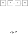
- FIG. 2 shows the corresponding configuration for a transmitter.
- the energy flow follows the same 'path' as for the receiver described above.
- the source is the transmitter 100, from where the energy flows to the phase shifter 20, then onto stub circuitry 50 and then is transmitted via antenna 110.
- the difference in use in a receiver or transmitter scenario concerns the relative direction of energy flow, as well as the relative magnitudes of the signals involved.
- the amount of energy flowing from the antenna 10 to the double stub matching circuit 50 via the phase shifter 20 is significantly smaller than the energy flow in the transmitter system shown in Figure 2 .
- FIG. 1 and 2 relate to receivers and transmitters respectively.
- a transceiver a transmitter and receiver
- This can be achieved in a known way e.g. using a duplexer or other technique which protects the receiver during a transmit operation.
- the transmit chain and receive chain will have separate phase shifters 20 and stub circuits 50, since it would be impractical to share them.
- the phase shifter 20 is required to deal with powers of vastly different magnitudes in a transmit scenario compared to a receive scenario.
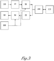
- FIG. 3 shows a transceiver system employing an impedance matching arrangement according to an embodiment of the present invention.
- the transceiver includes a transmit chain 100, 20, 50, a receive chain 60, 50, 20, a duplexer 200 and a common antenna 210. There is also shown a controller 300.
- the receive chain and transmit chain operate as set out previously. Each is connected to a duplexer 200, which is operable to ensure that only one of the receive chain and transmit chain is connected to the antenna at any given time. There are a number of different ways to implement such a function and the skilled person will be aware of an appropriate option for any given scenario.
- the antenna 210 is a shared antenna, used for transmitting and receiving. It may further be shared with another service, as described previously.
- a controller 300 This supplies a control signal to both of the phase shifters 50 so that an appropriate phase shift may be applied, dependent on the particular channel in use at that time.
- the controller 300 may be an integral part of the transceiver or it may be a stand-alone device, which receives channel information from the transceiver.
- the signal supplied from the controller 300 to the phase shifters 50 may be in the form of a digital signal or an analogue voltage, depending on the particular configuration of phase shifter employed.
- the channel number may be used to retrieve a control signal value from a look up table, with the retrieved control signal being supplied as required.
- Embodiments of the invention are operable to make use of limited facilities, for example on a maritime vessel, with minimal adaptation of the existing equipment.
Landscapes
- Transmitters (AREA)
Priority Applications (6)
| Application Number | Priority Date | Filing Date | Title |
|---|---|---|---|
| EP18275038.0A EP3540940A1 (fr) | 2018-03-13 | 2018-03-13 | Améliorations apportées ou se rapportant à une adaptation d'impédance |
| AU2019233937A AU2019233937B2 (en) | 2018-03-13 | 2019-03-06 | Improvements in and relating to impedance matching |
| US16/980,199 US11070188B2 (en) | 2018-03-13 | 2019-03-06 | Impedance matching |
| PCT/GB2019/050625 WO2019175544A1 (fr) | 2018-03-13 | 2019-03-06 | Améliorations apportées et relatives à l'adaptation d'impédance |
| EP19709553.2A EP3766175A1 (fr) | 2018-03-13 | 2019-03-06 | Améliorations apportées et relatives à l'adaptation d'impédance |
| CA3093767A CA3093767C (fr) | 2018-03-13 | 2019-03-06 | Ameliorations apportees et relatives a l'adaptation d'impedance |
Applications Claiming Priority (1)
| Application Number | Priority Date | Filing Date | Title |
|---|---|---|---|
| EP18275038.0A EP3540940A1 (fr) | 2018-03-13 | 2018-03-13 | Améliorations apportées ou se rapportant à une adaptation d'impédance |
Publications (1)
| Publication Number | Publication Date |
|---|---|
| EP3540940A1 true EP3540940A1 (fr) | 2019-09-18 |
Family
ID=61655710
Family Applications (1)
| Application Number | Title | Priority Date | Filing Date |
|---|---|---|---|
| EP18275038.0A Ceased EP3540940A1 (fr) | 2018-03-13 | 2018-03-13 | Améliorations apportées ou se rapportant à une adaptation d'impédance |
Country Status (1)
| Country | Link |
|---|---|
| EP (1) | EP3540940A1 (fr) |
Citations (4)
| Publication number | Priority date | Publication date | Assignee | Title |
|---|---|---|---|---|
| US5065118A (en) * | 1990-07-26 | 1991-11-12 | Applied Materials, Inc. | Electronically tuned VHF/UHF matching network |
| US5077499A (en) * | 1990-04-18 | 1991-12-31 | Mitsubishi Denki Kabushiki Kaisha | High-frequency feeding method for use in plasma apparatus and device for carrying out the method |
| US20040104785A1 (en) * | 2002-12-02 | 2004-06-03 | Park Pil Jae | Variable impedance matching circuit |
| US20090109880A1 (en) * | 2007-10-31 | 2009-04-30 | Hong Teuk Kim | Impedance control apparatus and method for portable mobile communication terminal |
-
2018
- 2018-03-13 EP EP18275038.0A patent/EP3540940A1/fr not_active Ceased
Patent Citations (4)
| Publication number | Priority date | Publication date | Assignee | Title |
|---|---|---|---|---|
| US5077499A (en) * | 1990-04-18 | 1991-12-31 | Mitsubishi Denki Kabushiki Kaisha | High-frequency feeding method for use in plasma apparatus and device for carrying out the method |
| US5065118A (en) * | 1990-07-26 | 1991-11-12 | Applied Materials, Inc. | Electronically tuned VHF/UHF matching network |
| US20040104785A1 (en) * | 2002-12-02 | 2004-06-03 | Park Pil Jae | Variable impedance matching circuit |
| US20090109880A1 (en) * | 2007-10-31 | 2009-04-30 | Hong Teuk Kim | Impedance control apparatus and method for portable mobile communication terminal |
Non-Patent Citations (1)
| Title |
|---|
| JOHN PAPAPOLYMEROU ET AL: "Reconfigurable Double-Stub Tuners Using MEMS Switches for Intelligent RF Front-Ends", IEEE TRANSACTIONS ON MICROWAVE THEORY AND TECHNIQUES, PLENUM, USA, vol. do51, no. 1, 1 January 2003 (2003-01-01), XP011076839, ISSN: 0018-9480 * |
Similar Documents
| Publication | Publication Date | Title |
|---|---|---|
| US10425115B2 (en) | Systems and methods for configurable hybrid self-interference cancellation | |
| US6194980B1 (en) | Quadrature hybrid RF combining system | |
| US10530033B2 (en) | Demultiplexer/multiplexer, antenna device, and fading elimination method | |
| EP2073393B1 (fr) | Transmetteur-récepteur | |
| US20130260844A1 (en) | Series-connected couplers for active antenna systems | |
| AU4111899A (en) | A radio transceiver and a method of preventing transmission spurious response | |
| US20170070368A1 (en) | Reflection coefficient reader | |
| US10382085B2 (en) | Analog self-interference cancellation systems for CMTS | |
| US10084496B2 (en) | Interference signal cancellation over a broad frequency range | |
| KR102233631B1 (ko) | 자기간섭신호 제거 장치 및 이를 포함하는 송수신기 | |
| US11070188B2 (en) | Impedance matching | |
| KR102424306B1 (ko) | 커플러 기반 전이중 무선통신 전단부 회로 및 그 제어방법 | |
| CA3093767C (fr) | Ameliorations apportees et relatives a l'adaptation d'impedance | |
| WO2020217388A1 (fr) | Circuit de synchronisation de phase | |
| GB2571943A (en) | Improvements in and relating to impedance matching | |
| US7336220B2 (en) | Method and apparatus for equalizing broadband chirped signal | |
| US7224244B2 (en) | Line-doubler delay circuit | |
| US20060198429A1 (en) | Isolating circuit of transmitting and receiving paths in same frequency carrier | |
| JPH02151130A (ja) | アンテナ共用器 | |
| CN112204893B (zh) | 数据传输系统 | |
| US20080076360A1 (en) | Apparatus for combining two radios on a single antenna | |
| CN108964679B (zh) | 功率容量提升方法、装置和设备 | |
| JPH1068770A (ja) | アクティブ・フェーズド・アレイ・レーダ装置 | |
| JP2002189045A (ja) | 反射電力モニタ回路とその調整方法 | |
| CN107147425A (zh) | 补偿电路及应用该补偿电路的天线单元 |
Legal Events
| Date | Code | Title | Description |
|---|---|---|---|
| PUAI | Public reference made under article 153(3) epc to a published international application that has entered the european phase |
Free format text: ORIGINAL CODE: 0009012 |
|
| AK | Designated contracting states |
Kind code of ref document: A1 Designated state(s): AL AT BE BG CH CY CZ DE DK EE ES FI FR GB GR HR HU IE IS IT LI LT LU LV MC MK MT NL NO PL PT RO RS SE SI SK SM TR |
|
| AX | Request for extension of the european patent |
Extension state: BA ME |
|
| STAA | Information on the status of an ep patent application or granted ep patent |
Free format text: STATUS: THE APPLICATION HAS BEEN REFUSED |
|
| 18R | Application refused |
Effective date: 20191007 |