EP3556600A1 - Dispositif et procédé d'étalonnage de dispositifs de détection d'objets - Google Patents
Dispositif et procédé d'étalonnage de dispositifs de détection d'objets Download PDFInfo
- Publication number
- EP3556600A1 EP3556600A1 EP19169790.3A EP19169790A EP3556600A1 EP 3556600 A1 EP3556600 A1 EP 3556600A1 EP 19169790 A EP19169790 A EP 19169790A EP 3556600 A1 EP3556600 A1 EP 3556600A1
- Authority
- EP
- European Patent Office
- Prior art keywords
- calibration
- ref
- characteristic
- electrical
- individual sensor
- Prior art date
- Legal status (The legal status is an assumption and is not a legal conclusion. Google has not performed a legal analysis and makes no representation as to the accuracy of the status listed.)
- Pending
Links
- 238000001514 detection method Methods 0.000 title claims abstract description 131
- 238000000034 method Methods 0.000 title claims abstract description 66
- 239000003990 capacitor Substances 0.000 claims abstract description 23
- 230000001419 dependent effect Effects 0.000 claims abstract description 13
- 238000005259 measurement Methods 0.000 claims description 108
- 238000011156 evaluation Methods 0.000 claims description 70
- 230000004044 response Effects 0.000 claims description 5
- 238000012546 transfer Methods 0.000 claims description 3
- 230000001939 inductive effect Effects 0.000 description 20
- 230000009897 systematic effect Effects 0.000 description 19
- 238000012545 processing Methods 0.000 description 15
- 230000009021 linear effect Effects 0.000 description 14
- 230000006870 function Effects 0.000 description 12
- 238000004364 calculation method Methods 0.000 description 10
- 230000008859 change Effects 0.000 description 10
- 230000008569 process Effects 0.000 description 10
- 230000008901 benefit Effects 0.000 description 7
- 239000011159 matrix material Substances 0.000 description 7
- 230000005540 biological transmission Effects 0.000 description 6
- 241000737052 Naso hexacanthus Species 0.000 description 5
- 230000006978 adaptation Effects 0.000 description 5
- 230000000694 effects Effects 0.000 description 5
- 238000013459 approach Methods 0.000 description 4
- 238000012937 correction Methods 0.000 description 4
- 238000011161 development Methods 0.000 description 4
- 230000018109 developmental process Effects 0.000 description 4
- 238000001914 filtration Methods 0.000 description 4
- 230000035484 reaction time Effects 0.000 description 4
- 230000003595 spectral effect Effects 0.000 description 4
- 241001136792 Alle Species 0.000 description 3
- 230000032683 aging Effects 0.000 description 3
- 238000004891 communication Methods 0.000 description 3
- 238000013461 design Methods 0.000 description 3
- 230000007274 generation of a signal involved in cell-cell signaling Effects 0.000 description 3
- 238000000926 separation method Methods 0.000 description 3
- 239000000243 solution Substances 0.000 description 3
- 238000012360 testing method Methods 0.000 description 3
- 230000003321 amplification Effects 0.000 description 2
- 238000004422 calculation algorithm Methods 0.000 description 2
- 230000003750 conditioning effect Effects 0.000 description 2
- 238000010586 diagram Methods 0.000 description 2
- 238000013507 mapping Methods 0.000 description 2
- 238000003199 nucleic acid amplification method Methods 0.000 description 2
- 230000000704 physical effect Effects 0.000 description 2
- 230000002265 prevention Effects 0.000 description 2
- 230000009467 reduction Effects 0.000 description 2
- 102100023444 Centromere protein K Human genes 0.000 description 1
- 101000907931 Homo sapiens Centromere protein K Proteins 0.000 description 1
- 206010061218 Inflammation Diseases 0.000 description 1
- 230000009471 action Effects 0.000 description 1
- 238000003491 array Methods 0.000 description 1
- 230000002457 bidirectional effect Effects 0.000 description 1
- 239000003985 ceramic capacitor Substances 0.000 description 1
- 238000012512 characterization method Methods 0.000 description 1
- 150000001875 compounds Chemical class 0.000 description 1
- 238000010276 construction Methods 0.000 description 1
- 125000004122 cyclic group Chemical group 0.000 description 1
- 230000003111 delayed effect Effects 0.000 description 1
- 230000007613 environmental effect Effects 0.000 description 1
- 238000010438 heat treatment Methods 0.000 description 1
- 230000006872 improvement Effects 0.000 description 1
- 230000006698 induction Effects 0.000 description 1
- 230000004054 inflammatory process Effects 0.000 description 1
- 238000009434 installation Methods 0.000 description 1
- 230000003993 interaction Effects 0.000 description 1
- 239000010410 layer Substances 0.000 description 1
- 239000000463 material Substances 0.000 description 1
- 229910052751 metal Inorganic materials 0.000 description 1
- 239000002184 metal Substances 0.000 description 1
- 150000002739 metals Chemical class 0.000 description 1
- 239000000203 mixture Substances 0.000 description 1
- 238000012544 monitoring process Methods 0.000 description 1
- 230000003287 optical effect Effects 0.000 description 1
- 230000000737 periodic effect Effects 0.000 description 1
- 230000001681 protective effect Effects 0.000 description 1
- 239000011241 protective layer Substances 0.000 description 1
- 230000035945 sensitivity Effects 0.000 description 1
- 238000007619 statistical method Methods 0.000 description 1
- 230000009466 transformation Effects 0.000 description 1
- 230000001052 transient effect Effects 0.000 description 1
- 238000009966 trimming Methods 0.000 description 1
Images

Classifications
-
- B—PERFORMING OPERATIONS; TRANSPORTING
- B60—VEHICLES IN GENERAL
- B60L—PROPULSION OF ELECTRICALLY-PROPELLED VEHICLES; SUPPLYING ELECTRIC POWER FOR AUXILIARY EQUIPMENT OF ELECTRICALLY-PROPELLED VEHICLES; ELECTRODYNAMIC BRAKE SYSTEMS FOR VEHICLES IN GENERAL; MAGNETIC SUSPENSION OR LEVITATION FOR VEHICLES; MONITORING OPERATING VARIABLES OF ELECTRICALLY-PROPELLED VEHICLES; ELECTRIC SAFETY DEVICES FOR ELECTRICALLY-PROPELLED VEHICLES
- B60L53/00—Methods of charging batteries, specially adapted for electric vehicles; Charging stations or on-board charging equipment therefor; Exchange of energy storage elements in electric vehicles
- B60L53/10—Methods of charging batteries, specially adapted for electric vehicles; Charging stations or on-board charging equipment therefor; Exchange of energy storage elements in electric vehicles characterised by the energy transfer between the charging station and the vehicle
- B60L53/12—Inductive energy transfer
- B60L53/124—Detection or removal of foreign bodies
-
- Y—GENERAL TAGGING OF NEW TECHNOLOGICAL DEVELOPMENTS; GENERAL TAGGING OF CROSS-SECTIONAL TECHNOLOGIES SPANNING OVER SEVERAL SECTIONS OF THE IPC; TECHNICAL SUBJECTS COVERED BY FORMER USPC CROSS-REFERENCE ART COLLECTIONS [XRACs] AND DIGESTS
- Y02—TECHNOLOGIES OR APPLICATIONS FOR MITIGATION OR ADAPTATION AGAINST CLIMATE CHANGE
- Y02T—CLIMATE CHANGE MITIGATION TECHNOLOGIES RELATED TO TRANSPORTATION
- Y02T10/00—Road transport of goods or passengers
- Y02T10/60—Other road transportation technologies with climate change mitigation effect
- Y02T10/70—Energy storage systems for electromobility, e.g. batteries
-
- Y—GENERAL TAGGING OF NEW TECHNOLOGICAL DEVELOPMENTS; GENERAL TAGGING OF CROSS-SECTIONAL TECHNOLOGIES SPANNING OVER SEVERAL SECTIONS OF THE IPC; TECHNICAL SUBJECTS COVERED BY FORMER USPC CROSS-REFERENCE ART COLLECTIONS [XRACs] AND DIGESTS
- Y02—TECHNOLOGIES OR APPLICATIONS FOR MITIGATION OR ADAPTATION AGAINST CLIMATE CHANGE
- Y02T—CLIMATE CHANGE MITIGATION TECHNOLOGIES RELATED TO TRANSPORTATION
- Y02T10/00—Road transport of goods or passengers
- Y02T10/60—Other road transportation technologies with climate change mitigation effect
- Y02T10/7072—Electromobility specific charging systems or methods for batteries, ultracapacitors, supercapacitors or double-layer capacitors
-
- Y—GENERAL TAGGING OF NEW TECHNOLOGICAL DEVELOPMENTS; GENERAL TAGGING OF CROSS-SECTIONAL TECHNOLOGIES SPANNING OVER SEVERAL SECTIONS OF THE IPC; TECHNICAL SUBJECTS COVERED BY FORMER USPC CROSS-REFERENCE ART COLLECTIONS [XRACs] AND DIGESTS
- Y02—TECHNOLOGIES OR APPLICATIONS FOR MITIGATION OR ADAPTATION AGAINST CLIMATE CHANGE
- Y02T—CLIMATE CHANGE MITIGATION TECHNOLOGIES RELATED TO TRANSPORTATION
- Y02T90/00—Enabling technologies or technologies with a potential or indirect contribution to GHG emissions mitigation
- Y02T90/10—Technologies relating to charging of electric vehicles
- Y02T90/14—Plug-in electric vehicles
Definitions
- the present invention relates to an apparatus for detecting objects (more precisely, detecting the presence of objects), and more particularly foreign matter.
- the device will be described with reference to a charging system for charging electrical equipment. It should be noted, however, that this device for detecting objects can also be used in other areas, for example in the detection of persons or living beings, but also in the detection of objects such as motor vehicles.
- the foreign bodies which can also be referred to as foreign objects, can be both inorganic bodies such as metals, as well as organic bodies.
- FOD Form Object Detection
- the basis of the FOD system is an active electromagnetic sensor system.
- Inductive sensors which are traversed by a time-variant current, generate a time-varying magnetic vortex field.
- Foreign objects brought into the area of action of the magnetic field experience an interaction with the same.
- the properties of the sensor are thereby changed.
- the present invention is therefore based on the object to provide a high precision of the foreign body detection even with occurring systematic errors or to ensure and thereby increase the security of such inductive charging devices.
- This object is achieved by the subject of the independent claims.
- Advantageous embodiments and further developments are the subject of the dependent claims.
- a further object of the invention is to make available a detection device which enables a precise and secure detection of objects, in particular a detection and / or detection of the presence of objects, even over long periods of time.
- a charging arrangement according to the invention for charging electrically operated devices has at least one primary coil, which is suitable and intended to generate a magnetic field, to transmit electrical energy inductively to a secondary coil, which is part of the electrically operated device.
- the charging arrangement is, in particular, a primary module which is suitable and intended to inductively supply a secondary module (for example a module having a secondary coil) of the object to be charged (for example a vehicle) with energy.
- a secondary module for example a module having a secondary coil
- the charging arrangement according to the invention on a detection device for detecting objects, wherein the detection means at least one signal generator which is suitable and intended, at least one individual sensor device comprising an electrical circuit, the at least one detection coil and / or at least one resistor and / or at least one Capacitor has to supply AC voltage, and an evaluation device (and / or a measuring device), which is suitable and intended to detect at least one of the individual sensor device (and / or for the electrical circuit) characteristic electrical variable.
- This is the characteristic of the individual sensor device (or for the electrical circuit) size preferably by phase information (and / or amplitude information) and this characteristic variable is preferably obtained on the basis of scattering parameter measurements of the electrical circuit (or of the individual sensor device (s)).
- the size characteristic of the individual sensor device is understood to mean a quantity of (among other things) at least one characteristic value, preferably a plurality of characteristic values (for example two characteristic values) of the series replacement image (or series replacement circuit) of (or at least a) individual sensor device (which consists for example of a series resistor and an inductor or this has) depends.
- the characteristic value may be, for example, the resistance value or the value of the inductance or the capacitance value of the series-equivalent circuit (or series-substitute image) of the individual sensor device.
- at least one measurement signal is sampled directly here.
- the characteristic quantity is determined by vectorial scattering parameter measurements of the electrical circuit (or of the individual sensor device (s)).
- the alternating voltage is preferably a sinusoidal voltage and generally a periodic alternating voltage.
- the alternating voltage is preferably the superposition of at least two or preferably a plurality of sinusoidal voltages (and / or cosine voltages).
- the signal generator may preferably be a frequency generator.
- the signal generator is suitable and determined to superimpose a plurality of alternating voltages such as sinusoidal voltages and / or cosine voltages.
- the signal or the AC voltage can be generated by a digital-to-analog converter.
- the detection device is suitable and determines at least one calibration device (preferably at least one first calibration device and at least one second calibration device) with (in each case) at least one calibration element, preferably with (respectively) at least three (different) calibration elements, in particular by the signal generator To supply AC voltage, wherein the evaluation device is suitable and intended to detect at least one of the (and preferably each) calibration element characteristic electrical variable (or to measure or determine).
- the charging arrangement is preferably suitable and intended to carry out the method described below or individual method steps described in this context or in combination.
- the evaluation device detects the characteristic size of the circuit (or of the individual sensor device (s)) by applying the same to the AC voltage and more precisely by detecting a reaction of the switching circuit (or the individual sensor device charged with the AC voltage). , the presence of a foreign body.
- the abovementioned coil of the detection device or of the individual sensor device (s) is / are also referred to below as the detection coil for the purpose of better delimitation from the primary coil.
- the detection device has at least one electrical component whose properties and in particular its current conduction properties change in the presence of a foreign body.
- this component may be a coil (or in general an inductance) and / or a capacitor (or in general a capacitive element).
- a resistor may be present.
- the detection device can preferably be a component of the charging arrangement, or be in firm connection with the primary module (or form part of the primary module). However, it would also be conceivable that the detection device is integrated into the secondary module of the object to be charged or that the detection device is a further module which is arranged, for example, between the primary module and the secondary module.
- the electrical and charging device is selected from a group of devices which include motor vehicles, in particular cars, motorcycles, household appliances, telecommunication devices, such as smartphones and the like.
- the charging arrangement on a power supply to supply the primary coil with electrical energy.
- the primary coil is operated with a primary voltage of a first frequency and the AC voltage source outputs an AC voltage of a second frequency and one of these two frequencies is at least twice as large as the other of the two frequencies.
- the frequencies which are used for the operation of the electrical circuit or resonant circuit on the one hand and which are used to operate the primary coil on the other hand significantly differ from each other, at least by a factor of 2.
- the frequency is the Operation of the circuit or resonant circuit is used much higher than the frequency, with which the primary coil is supplied.
- one of said frequencies is at least five times as large as the other, preferably at least ten times as large, more preferably at least one hundred times as large. In this way it can be achieved that even during operation of the primary coil of the electrical resonant circuit is not significantly influenced by the influence of the primary coil b whose magnetic field.
- the primary coil and the detection coil are arranged in a predetermined fixed position to each other.
- the sensitive part can also be a capacitor.
- a (second) sensor network may also be mounted in the car module.
- the primary coil and the detection device may be arranged on a common carrier and / or on a common housing.
- a protective element is provided, which protects the primary coil as well as the detection coil device or the electrical circuit and / or the electrical resonant circuit from direct contact.
- a thickness or resistance of this protective layer may depend on the particular requirements. For example, the field of application of the detection device or the field of application of the charging arrangement.
- the charging arrangement has a control device which controls an energization of the primary coil in dependence on an output signal of the detection device. If, for example, it follows from this output signal that there is a foreign body between the primary coil and the secondary coil or in the region of the primary coil, then (primary) energization of the primary coil can be prevented or a current supply for the primary coil can be switched off, in this way Prevent hedging risks.
- the device may comprise an information output device which informs the user of a foreign body in a physically perceptible manner. More specifically, it is possible that the sensor also provides a pre-detection before the loading operation (because the sensor just can also detect independently of the operation of the primary coil). This distinguishes it from other known sensor systems. Here is one of the great strengths of the invention to see.
- the charging arrangement has at least one A / D converter which samples an analog signal.
- the phase information is obtained on the basis of the scatter parameters by detecting the scatter parameters by means of algorithms as complex variables.
- a signal conditioning is provided which provides the microcontroller with a processed analog signal.
- This output device can output, for example, an audible alarm signal, which indicates to the user that a foreign body is in the region of the primary coil. Furthermore, it is also possible that during the detection of a foreign body is switched off during operation, in particular the current charging operation or switching is prevented. Furthermore, it is possible that the primary coil and the detection coil are operated together. However, it is also possible that the detection coil is operated outside the operation of the primary coil. Furthermore, a control device may be provided, which performs measurements on foreign bodies at predetermined time intervals or at discrete times, for example in a predetermined timing.
- the present invention is further directed to a detection device for detecting objects, wherein the detection device at least one signal generator which is suitable and intended, at least one individual sensor device comprising an electrical circuit (and in particular a resonant circuit), the at least one detection coil and / or at least a resistor and / or at least one capacitor, to supply with AC voltage, and having an evaluation device which is suitable and intended to detect at least one characteristic of the individual sensor device electrical quantity.
- the detection device has at least two coils or at least two detection coils.
- the detection device has at least one capacitor.
- the detection device may, for example, comprise a measuring device, which is one of the (preferably each) resonant circuit (or of at least one individual sensor device and preferably from each individual sensor device) measures electrical signal. If necessary. the measuring device and / or the sensor device has at least one directional coupler. Preferably, however, a measuring device and / or sensor device is used which operates without the use of a directional coupler.
- the detection device is suitable and determines at least one calibration device (and preferably at least one first calibration device and / or at least one second calibration device) with (in each case) at least one calibration element (and preferably with at least three calibration elements) in particular by the signal generator with alternating voltage
- the evaluation device is suitable and intended to detect at least one electrical variable that is characteristic of the (and preferably one for each) calibration element.
- the detection device preferably has a measuring device which measures at least one electrical variable characteristic of the (and preferably one for each) calibration element.
- the detection device is preferably suitable and determines to carry out the method steps described above in connection with the method for detecting objects, individually or in combination, and vice versa.
- the detection device may have the feature described above in connection with the charging arrangement individually or in combination, and vice versa.
- a characteristic of a calibration electrical variable is preferably an amplitude information and / or phase information, which in particular (each) depending on the frequency of the exciting signal or the AC voltage, and this characteristic size is preferably based on (vector ) Scattering parameter measurements on this calibration obtained.
- vectorial is preferably understood a measurement by amplitude and phase.
- An application of this detection device can thus again be a charging device for charging vehicles, for example.
- the detection device it is also possible to detect other objects, as mentioned above, for example of living beings or of vehicles or the like.
- live object detection can also work with the "simple” variant with only one network or circuit.
- live object detection can also work with the "simple” variant with only one network or circuit.
- the circuit is preferably not a so-called integrated circuit (IC).
- the object can be both an organic and an inorganic object.
- these objects can be metallic objects, but also non-metallic objects. It is also proposed here that it is determined how a behavior of the circuit or resonant circuit and in particular its natural frequency changes due to the said object.
- the resonant circuit has a plurality of detection coils (for each resonant circuit preferably always includes exactly one coil or a plurality of series and / or parallel coils) preferably at least four coils, preferably at least five coils and preferably at least six coils.
- the detection device has an even number of coils and / or individual sensor devices (each having a coil).
- the coils or coil areas may each be wound in pairs in different directions, so that in the aggregate the coils are not influenced by a magnetic field originating, for example, from the primary coil.
- the presence of a foreign body usually only affects one of the mentioned coils.
- coils of a resonant circuit are preferably arranged in series. However, it would also be possible that several coils are arranged in parallel within the scope of a resonant circuit.
- a first group of oscillating circuits and in particular the coils of these oscillating circuits, to extend in a first predetermined direction.
- a first group of oscillating circuits to extend in a first direction and for a second group of oscillating circuits to extend in a second direction, in particular in a direction perpendicular to the first direction. In this way it would be possible that a relatively accurate position of the objects is detected.
- the position of the object can be determined, for example, it can be assumed that the object is based on a resonant circuit extending in the first direction and a second resonant circuit, in a second to the first vertical direction extends affects.
- the frequency of the signal generator in a predetermined frequency range or frequency band is tunable.
- At least one frequency is preferred and all frequencies are particularly preferably selected from a range around 1 MHz.
- the sensor device and / or the individual sensor device (s) and / or (first and / or second) calibration device are subjected in particular sequentially to AC voltage of different frequencies.
- at least ten, preferably at least twenty, preferably at least thirty and more preferably 32 and / or preferably at most 50 different frequencies are preferably selected for this purpose.
- These are preferably selected from a range between 500 kHz and 1 MHz, preferably from a range between 600 kHz and 900 kHz and more preferably from a range between 700 kHz and 900 kHz.
- a capacitance of the or at least one capacitor of the circuit is between 20 pF and 1nF, preferably between 50 pF and 500 pF and preferably between 100 pF and 300 pF.
- a capacitance of the or at least one capacitor of the circuit can be between 1 nF and 50 nF, preferably between 3 nF and 30 pF, and preferably between 4 nF and 20 nF.
- the at least one capacitor is selected from a group of capacitors containing film capacitors, ceramic capacitors and the like.
- so-called capacitance diodes could be used whose capacity is variable.
- the device has an A / D converter to convert analog signals into digital signals.
- the signal generator generates a frequency changeable output voltage.
- a frequency with which or the electrical oscillator circuits are controlled can be controlled in a specific range and in particular a specific range around a resonant frequency.
- the detection device has a control device which controls the frequency of the output voltage of the signal generator in a predetermined frequency range.
- a frequency of the signal generator in a certain frequency range can be tuned.
- the frequency could be controlled within a range of +/- 50 kilohertz (+/- 50 kHz) by a natural frequency of the resonant circuit.
- the evaluation device and / or the measuring device allows detection of only one parameter or only a few characteristics of the circuit or network.
- the circuit could be a two-terminal.
- it could also be a quadrupole, with only about two values of this quadrupole being measured, such as its S11 and its S21 parameter.
- the measuring device and / or the evaluation device and / or the individual sensor device (s) has at least one directional coupler in order to tap off at least a portion of a voltage from the circuit.
- an embodiment which dispenses with the use of directional couplers is preferred (cf. Fig. 10 ).
- at least one directional coupler is a unidirectional directional coupler.
- at least one of these directional couplers is a bidirectional directional coupler.
- the evaluation device has at least one measuring device for measuring a current intensity or a voltage.
- this measuring device is parallel to the mentioned circuit or resonant circuit.
- the characteristic of the resonant circuit size is selected from a group of electrical variables, which includes an attenuation of the circuit or resonant circuit, a power loss of the circuit or oscillating circuit and the like.
- the detection device also serves for the non-optical detection of foreign bodies and / or objects.
- the at least one and preferably the at least two detection coils are arranged on a circuit board and particularly preferably printed on this circuit board.
- This procedure has proven to be particularly space-saving.
- the turns of the coil are preferably arranged in at least one plane, preferably in exactly one plane. This leads to a cost reduction because a PCB with fewer layers is less expensive.
- a space reduction can be achieved. This can be achieved as mentioned, for example, by printing on a board.
- the capacitor or capacitors can / can be arranged on the board (or even the entire measuring electronics).
- a plurality of coils are arranged in one plane and preferably all coils are arranged in one plane.
- the device has a plurality of electrical circuits or oscillating circuits and a switching device which causes these circuits or oscillating circuits to be subjected sequentially to an alternating voltage and in particular to the alternating voltage of a signal generator.
- this switching device is a so-called multiplexer.
- the switching device (also) is designed as a sensor interface.
- the detection device has an (inductive) sensor device, which in particular at least one (inductive) single sensor device and preferably a plurality of (inductive) single sensor devices (preferably each with a circuit and in particular resonant circuit preferably comprising at least one coil and / or at least one capacitor and / or at least one resistor).
- each individual sensor device has at least one coil and at least one resonant adjustment device (hereinafter also referred to as resonant adaptation), in particular for adaptation and / or adjustment of the resonant frequency (of the oscillating circuit or of the individual sensor device), the resonant adapting device preferably being suitable and is determined to act as a filter and / or to adapt a performance of the individual sensor device.
- the individual sensor devices are also referred to as individual sensors or sensor fields.
- at least two, preferably at least ten, preferably at least 16, preferably at least 32 and particularly preferably at least 64 and / or at most 256 and preferably at most 128 and particularly preferably at most 64 individual sensor devices are provided.
- each individual sensor device is connected to the evaluation device and / or the signal generator and / or the measuring device (electrically) and / or connectable.
- each individual sensor device (the sensor device) is preferably connected to a sensor interface and / or one / of the switching device (multiplexer) (electrically) and / or can be connected to the signal generator via this sensor interface.
- the calibration device has at least three calibration elements, which preferably differ from one another in pairs in at least one electrical property or their electrical properties, in particular with respect to their current conductivity.
- the (at least three) calibration elements differ with respect to their electrical resistance.
- the calibration elements are precision resistors. This offers the advantage that these over a longer period of time a given resistance value within very small tolerances ensure their usefulness as a reference. In principle, all resistance values, which preferably differ sufficiently from one another, can be selected for this purpose.
- a calibration element has a resistance (value) of 0 ohms (short circuit) and / or a calibration element has a resistance (value) of infinite ohms (open circuit) and / or a calibration element has a resistance (value) of substantially 50 ohms (exactly) 50 ohms.
- the calibration device is at least one detachably or temporarily connectable to the detection device (and / or the signal generator and / or the measuring device and / or the evaluation device) (wherein preferably at least one part or unit of the Calibration device and particularly preferably at least two and preferably to all (separate) parts or units in particular sequentially (but not simultaneously) such a compound is prepared or can be produced) and / or preferably separable from the detection device calibration device, which hereinafter also as first calibration device or (also) as a basic calibration device (or as a calibration device for performing a basic calibration) is called.
- the first calibration device can be separated mechanically and / or electrically from the detection device and in particular from the (or at least one) signal generator of the detection device and / or a sensor interface of the detection device and / or the evaluation device and / or the measuring device.
- the first calibration device is manually separable from the detection device and / or the sensor device.
- a electrical connection between at least one calibration element (preferably all calibration elements) of the first calibration device and the sensor interface of the detection device can be produced via a plug connection.
- At least one calibration element of the first calibration device is preferably arranged on a different or separate base body or circuit board in comparison to the signal generator. In particular, the first calibration device is thus not arranged on the (evaluation) board on which the evaluation device (with the signal generator) is arranged.
- the basic calibration device or the first calibration device has at least one, preferably at least two, preferably at least three and particularly preferably exactly three calibration units.
- the calibration units are preferably in particular successively in each case with the detection device and / or the signal generator and / or the evaluation device (mechanically and / or electrically) (via the same sensor interface of the detection device) connectable. It is possible that the different calibration units are separate and / or (mechanically and / or electrically) not (pairwise) interconnected elements.
- Each calibration unit preferably has at least one calibration element.
- each calibration unit has a multiplicity of calibration elements, with the number of calibration elements and, preferably, of each calibration device particularly preferably corresponding to the number of individual sensor devices.
- each calibration unit preferably has at least two, preferably at least ten, preferably at least 16, preferably at least 32 and particularly preferably at least 64 and / or at most 256 and preferably at most 128 and particularly preferably at most 64 calibration elements.
- each calibration unit has identical and / or identical and / or the same electrical resistance having calibration elements.
- at least two calibration units and preferably all calibration units have (with regard to their current-carrying properties and preferably in their electrical resistance values) calibration elements differing from each other.
- the first calibration device is preferably not arranged on the detection device and / or the charging arrangement or connected to it (mechanically and / or electrically).
- the detection device has (at least) one (and preferably exactly one) permanently connected to it calibration device, which is referred to as a second calibration device (or as a calibration device for performing the calibration at run time).
- the second calibration device is (permanently) mechanically and in particular also permanently connected to the detection device and in particular to the evaluation device and / or the measuring device and / or the signal generator and / or preferably arranged stationary on the detection device.
- the second is preferred Calibration device and in particular at least one calibration element thereof arranged on the (evaluation) board on which also the signal generator and / or at least partially the measuring device and / or at least partially the evaluation device is arranged.
- the second calibration device is preferably suitable and intended for remaining on or on the detection device.
- the second calibration device preferably has at least two and preferably at least three and particularly preferably exactly three calibration elements.
- the (preferably three) calibration elements preferably each have (in pairs) different resistance values and / or current-conducting properties.
- the calibration elements of the second calibration device are not identical or identical components.
- a calibration element of the second calibration device has a resistance value of 0 ohms (short circuit) and / or a calibration element of the second calibration device has a resistance value of infinity ohms (idle) and / or a calibration element of the second calibration device has a resistance of substantially 50 ohms or (exactly ) 50 ohms.
- the number of calibration units of the first calibration device preferably coincides with the number of (preferably different and / or with the total number of) calibration elements of the second calibration device.
- at least one and preferably each calibration element of the second calibration device is identical and / or identical to at least one and preferably each calibration element of (preferably exactly) a calibration unit of the first calibration device and / or preferably correspondingly have identical current conduction properties and / or identical electrical resistance.
- This offers the advantage that in the context of the calibration over the first calibration device and over the second calibration device (respectively) identical calibration elements are used. This offers the advantage of a more direct comparability or an identical electrical behavior and / or preferably an expected same time aging or change of the calibration elements.
- the second calibration device can also have at least one calibration element and preferably all calibration elements with different current-conducting properties or electrical resistances (in each case) relative to the calibration elements of the first calibration device.
- the detection device is suitable and determines that in particular at the same time (at least partially) the first calibration device (or at least one calibration unit the first calibration device) and (preferably completely) the second calibration device (or at least at least three calibration elements of the second calibration device) are arranged on it or connected to it (and / or to the evaluation device) (mechanically and / or electrically).
- the detection device is suitable and determines that the second calibration device (or at least at least three calibration elements of the second calibration device) and the sensor device or at least one individual sensor device and preferably all individual sensor devices (of the sensor device) are arranged or arranged at it at the same time (preferably completely) are connected to it (and / or to the evaluation device) (mechanically and / or electrically).
- the first calibration device (or at least one calibration unit of the first calibration device) or (exclusively or) the sensor device or at least one individual sensor device is arranged on or connected to the detection device.
- the first calibration device (or its calibration units and / or calibration elements) is preferably not connected to the detection device and in particular to the signal generator and / or the measuring device and / or or in particular the evaluation device connected.
- the second calibration device or at least one calibration element of the second calibration device with the detection device and in particular the signal generator and / or in particular the measuring device and / or in particular the evaluation device is preferred in particular during the performance of a measurement on at least one circuit or oscillating circuit or at least one individual sensor device (at least mechanically and preferably electrically) connected.
- the evaluation device is suitable and determines, as a function of an electrical variable characteristic of the individual sensor device, whether there is a movable object in the vicinity of the individual sensor device (or sensor device) with respect to this individual sensor device (or sensor device), wherein in this determination at least one calibration variable is taken into account, which is dependent on at least one characteristic of the calibration element electrical variable.
- the detection device and in particular the evaluation device has a memory device in which the electrical variables detected and / or measured by the evaluation device and / or measuring device (characteristic of at least one calibration element (preferably for all calibration elements) of the first and / or second calibration device and / or characteristic for at least one individual sensor device (and preferably for all individual sensor devices) and / or calculated or determined calibration variables can be stored and / or retrieved.
- the detection device and in particular the evaluation device preferably has a processor or a computing device which preferably determines at least one calibration variable characteristic for an individual sensor device (in particular for each individual sensor device) or at least one calibration variable for the individual sensor device (in particular for each individual sensor device). or calculated.
- the determination and / or calculation is preferably carried out as a function of and / or taking into account at least one characteristic electrical variable (measured and / or detected) for individual sensor device (s) and / or taking into account at least one measured (and / or measured) for the first calibration device. or detected) characteristic electrical quantity and / or at least one for the second calibration device (measured and / or detected) characteristic electrical variable.
- the determination and / or calculation is preferably carried out as a function of at least one, preferably at least two and particularly preferably at least three electrical variables characteristic of (each) one (other) calibration element of the second calibration device.
- the determination and / or calculation is preferably carried out as a function of at least one, preferably at least two and particularly preferably at least three electrical variables characteristic of (in each case) one calibration element (another calibration unit) of the first calibration device.
- the present invention is further directed to a method for detecting objects, in particular in charging arrangements for charging electrically operated devices, by means of a detection device, the method comprising applying at least one individual sensor device comprising an electrical circuit (in particular resonant circuit), the at least one detection coil and / or at least one resistor and / or at least one capacitor (preferably with at least two coils and / or at least one capacitor) comprises (from a signal generator or frequency generator) with an alternating voltage and measuring at least one characteristic of the individual sensor device electrical variable.
- the electrically operated devices are preferably mobile devices and particularly preferably vehicles, for example motor vehicles. In particular, it is also particularly preferred in terms of the method Foreign body that is not intended in the vicinity of said circuit or resonant circuit.
- At least one calibration element is subjected to alternating voltage and at least one electrical variable characteristic of this calibration element is determined, depending on this characteristic variable for the individual sensor device, whether in the environment of the individual sensor device (and / or the sensor device) opposite to this individual sensor device (and / or the sensor device) movable object is located, wherein in this determination at least one calibration is taken into account, which is dependent on at least the electrical variable characteristic of the calibration.
- a frequency of the signal generator is changed to detect the objects and in particular that frequency with which the at least one resonant circuit is applied.
- the frequency is tuned in a predetermined frequency range or frequency band.
- At least two coils connected in parallel or in series are operated or acted upon by the alternating voltage.
- the forward voltage can be taken into account, which results from the value S21 explained in more detail below.
- a natural frequency of the resonant circuit is determined, in particular also as a function of the presence of the object to be detected.
- At least three, in particular in pairs at least in an electrical property of each other different, calibration elements are subjected to AC voltage.
- an electrical variable characteristic for the respective calibration element is preferably measured, the calibration variable being dependent on at least these three characteristic electrical variables.
- the calibration variable is preferably selected as a function of at least one, preferably at least two, and particularly preferably at least three measured, electrical (n) characteristic (s) for one (other) calibration element (the first calibration device and / or the second calibration device) ) Size (s) determined or calculated.
- a first calibration of at least one measuring method of the detection device is carried out by means of a first calibration device, and a further calibration of the measuring method is carried out by means of a second calibration device, in particular delayed in time or chronologically thereafter.
- an object detection method of the detection device is thereby calibrated.
- the at least one further and preferably at least two further and preferably at least two further and preferably a multiplicity of further calibrations carried out by the second calibration device take place, taking into account the results of the first calibration by the first calibration device.
- the first calibration device is preferably used once (a basic calibration) (possibly with the aid or use of the second calibration device). Further calibrations (at later times) then preferably take place exclusively using the second calibration device, ie without (re) using or carrying out measurements on the first calibration device (at these later times).
- the basic calibration performed once with the first calibration device and, in particular, the characteristic electrical variables and / or calibration variables and / or results obtained therein are used and at least partially taken into account in the calculation of the calibration variable ,
- the further calibration carried out by means of the second calibration device (which preferably takes place at a later time than the basic calibration or a calibration by means of the first calibration device takes place) without using the first calibration device.
- a ratio is preferably formed from at least one characteristic variable (detected or measured) for a calibration element of the second calibration device and at least one characteristic variable determined (measured or measured) for the same calibration element at a later point in time.
- the further calibration carried out by means of the second calibration device is based on at least one and preferably three permanently arranged on the detection device and in particular electrically connected to at least one component of the detection device calibration elements.
- the first calibration device for performing the first calibration is or is detachably connected to the detection device, in particular to one or a (or via) sensor interface for the electrical connection of the individual sensor device and / or a sensor device to a signal generator ,
- At least two and preferably a plurality of further calibrations are carried out by means of the second calibration device.
- the measuring cycle is preferably understood to be the successive or (immediately) consecutive measurement or detection of characteristic electrical variables of a plurality (preferably all) of individual sensor devices.
- precisely one characteristic electrical variable is thus detected or measured in a measuring cycle for each individual sensor device (preferably in each case for each predefined frequency).
- At least one and preferably exactly one (running time) calibration measurement takes place after each measurement cycle (preferably in each case for each predetermined frequency), whereby at least one and in particular exactly one characteristic electrical one for each calibration element of the second calibration device Size is measured or measured.
- three Einzelkalibrier pileen take place preferably after a measuring cycle, in each of which a characteristic of each calibration of the second calibration device electrical variable is detected or measured. For example, in the case of 64 individual sensor devices, the successive measurement of the individual sensor device may be followed by three individual calibration measurements (of the three calibration elements of the second calibration device).
- a calibration measurement by means of the second calibration device preferably in each case for each predefined frequency, in which preferably (at least and preferably exactly) an electrical variable characteristic of each calibration element of the second calibration device is detected or measured.
- a calibration measurement is carried out by means of the second calibration device (in which preferably (at least and preferably exactly) one electrical variable characteristic of each calibration element of the second calibration device is detected or measured) at fixed time intervals (which can preferably be predetermined or initiated by a timing device) ).
- calibration measurements can be made by means of the second calibration device after every one second. This offers the advantage that, for example, after a period of time of 10 s, expected changes can be monitored or controlled or taken into account.
- the fixed time intervals between two successive are preferably selected from a range between 1/10 s and 10 min, preferably between 1/5 s and 1 min and particularly preferably between 1 ⁇ 2 s and 5 s.
- the determination of at least one calibration variable and particularly preferably all calibration variables takes place on the basis of a linear error model.
- a calibration (of a non-calibrated or measured) variable is performed by a linear mapping or a linear transformation.
- a (electrical) variable (for an individual sensor device) characteristic of a traveling (normalized) wave size and / or a characteristic (electrical) variable characteristic of a returning (normalized) wave size (for this individual sensor device) is preferably linearly transformed or imaged.
- Preferred is a linear representation represented by a matrix, preferably represented by a 2x2 matrix of a vector made up of a variable (electrical) quantity characteristic of a traveling (normalized) wave size (for a single sensor device) and of a (electrical) variable characteristic of a returning (normalized) wave size (for this single sensor device) (for calibration).
- a matrix preferably represented by a 2x2 matrix of a vector made up of a variable (electrical) quantity characteristic of a traveling (normalized) wave size (for a single sensor device) and of a (electrical) variable characteristic of a returning (normalized) wave size (for this single sensor device) (for calibration).
- Preferably (at least three, and more preferably exactly three) of the entries of the matrix are determined by means of the first calibration device and / or by means of the second calibration device.
- the characterization of the electrical sensor properties is carried out by the vectorial measurement of scattering parameters on bipolar sensors.
- Scattering parameters that describe a two-pole or a one-port are limited to S 11 equivalent to the reflection factor ⁇ .
- He describes the ratio of reflected wave b i to the outgoing wave a i and fully characterizes the linear properties of a gate.
- the reflection factor can be converted without restrictions to the input impedance of a single gate. The common representation of this size is in the frequency domain.
- the evaluation of the measurement signals is based on the above-described change in the electrical sensor properties (or the change in the electrical properties of the sensor device 10 or the individual sensor devices 43), which consequently result in a change in the measured reflection factors.
- suitable evaluation parameters it would be possible to draw conclusions about foreign objects, or their size, location and their material, and thus fulfill the function of a foreign object recognition.
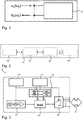
- FIG. 1 Fig. 3 is an illustration of the scattering parameters a i ( ⁇ i ), b i ( ⁇ i ) on a two-pole or sensor dipole 10 (which may be approximately part of a sensor device 40).
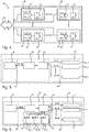
- the FOD system 20 (or also detection device 20) (FOD Foreign Object Detection), shown in FIG. 2 , is preferably in an evaluation electronics 30 (or evaluation device 30, wherein the evaluation device 30 is hereinafter referred to as evaluation electronics) and an inductive sensor unit 40 (or sensor device 40, which is also referred to below as a sensor unit) to divide.
- evaluation electronics 30 or evaluation device 30, wherein the evaluation device 30 is hereinafter referred to as evaluation electronics
- an inductive sensor unit 40 or sensor device 40, which is also referred to below as a sensor unit
- the evaluation electronics 30 are preferably in communication with a (higher-level) control unit 50 or a (higher-level) control unit 50.
- the sensor unit 40 may preferably detect an object in the monitored space 60 adjoining the control unit 50.
- the evaluation electronics 30 preferably forms the core of the system and contains the complete functionality for sequentially measuring a defined number N of sensors on inductive sensors 43 (which are also referred to as individual sensor devices 43) and for inferring possible foreign objects. It also forms the interface to the other system components of the inductive charging system in order to be able to pass on messages about detection events.
- Inductive sensor unit 40 in FIG Figure 4 provides the actual sensors.
- the entire unit consists of a defined number of in particular planar printed inductors 41 or coils 41, which together cover the entire surface to be detected.
- Resonance adjustments 42 are preferably connected to the sensor coils (filtering effect, power adjustment sensor, etc.).
- FIG. 4 shows a block diagram of the sensor unit or sensor device 40th
- the combination of inductance and resonance adaptation forms individual sensor (s) 43, which are also referred to below as sensor fields.
- the shape, size and composition of these sensor coils determine the generated magnetic field and thus also the space in which foreign objects can be detected.
- Each field is separately connected to the evaluation electronics, preferably via an interface 34.
- the sensor fields are excited and measured one after the other with a measurement signal during a measurement process.
- Each sensor field will measure a defined time T meas .
- a defined break T break is observed between the measurements of individual sensor fields (switch multiplexer, buffer digitized values, transient process next sensor field).
- T cycle essentially determines the reaction time of the system. If the measured values are additionally averaged or filtered in a later processing, the reaction time is additionally increased by one factor.
- the measuring system is designed such that the complete processing of the recorded data from field n takes place at the time of recording the data from field n +1 . Since no further pause or delay times occur apart from the times described above, it is possible to speak of a real-time measuring system with a defined reaction time.
- the aim of the system is to measure electrical parameters of the sensor coils. It can be assumed that these parameters change only slightly with small foreign objects (for example, relative inductance change ⁇ 0.1% in the case of a foreign object paper clip). As a result, the measured values must be recorded with great precision in order to be able to estimate changes in a further signal processing and draw conclusions about the way in which the changes are made. Measurement errors would massively distort these results or make further processing of the data impossible. For this reason, a strategy must be developed to prevent or minimize measurement errors as much as possible. This requires a deeper understanding of the nature and origins of errors, which will be discussed in more detail below.
- the errors described can be characterized by statistical methods and minimized by different approaches.
- the reflection factor is generally a frequency-dependent variable
- the measurement must be made for each measurement frequency ( ⁇ i ) and each sensor field.
- the index Sn which belongs to the n . Sensor field expresses. Based on the knowledge of the reflection factors, the further signal processing can take place (eg estimation of the electrical sensor properties ⁇ consideration of changes ⁇ foreign object recognition).
- a digital processing (means) 35, an analog processing (means) 38 and the signal distribution 33 are shown as elements of the evaluation electronics 30. Furthermore, a sensor device 40, which is arranged on the evaluation electronics 40 or is electrically connected thereto, is shown with a plurality of individual sensor devices 43 or 43_1, 43_2, 43_N.
- a linear error model was developed, which maps the measured quantities by complex valued error coefficients to the true values by a linear equation.
- Systematic errors from 1,3,4,5 described in 2.1.2 can be corrected.
- the basic assumption of this model is that the system itself can be considered linear.
- ⁇ can be called an "absolute error coefficient”.
- the challenge now is to precisely determine the error coefficients ⁇ , ⁇ , ⁇ of the relative error matrix for each sensor field and each measurement frequency at each instant.
- the relative calibration of the FOD system is similar to a classical calibration of a vectorial network analyzer (e.g., SOLT).
- the three error coefficients can be determined by measuring at least three known test objects (instead of the inductive sensor unit).
- any error coefficient can be determined.
- indices i expressing the frequency dependence of the measurement frequency ⁇ i are omitted below for reasons of better readability. Building on this point However, all other variables are to be considered as frequency dependent without restriction.
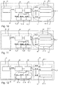
- FIG. 6 shows a signal flow plan FOD with calibration units.
- the reference numeral 74 denotes the second calibration device, which is preferably fixedly arranged on the evaluation electronics 30 and has at least one calibration element 76 and preferably three different calibration elements 76_A, 76_B, 76C.
- the reference numeral 70 generally indicates the first calibration device, which in turn has three (separate) calibration units 70_A, 70_B and 70_C (see FIG Figures 7-9 ). Each of these calibration units preferably has a plurality of, and preferably N, in particular identical or identical calibration elements 72_A or 72_B or 72_C.
- Indices G / M indicate valid values for the basic calibration or later measurement, ie at runtime.
- the error coefficients of the sensor fields at the time of the measurement ⁇ ⁇ L, Sn , ⁇ L, Sn , ⁇ L, Sn ⁇ are necessary for the later calculation of the reflection factors, but for the time being unknown.
- the calibration element B (reference numeral 72_B) is measured in each case.
- Total N measurements for N sensor fields. For each sensor field and each measurement frequency you get the ratio b G . sn a G . sn Calf M . sn S 1 . S 2 . ... . SN
- FIG. 10 shows a basic calibration with measurement of the calibration elements A, B and C (see reference numerals 72_A, 72_B and 72_C) and the second calibration device 74 on reference path (illustrated by ellipse E1).
- the sensor fields 1 to N are measured periodically in the first place.
- This measuring process is now extended by inserting calibration procedures. Since it can be assumed that system changes take place only slowly (constant over a few seconds), it is generally not necessary to carry out a calibration procedure after each measurement. In each case one calibration procedure can be carried out on a number of M measuring processes.
- the calibration operations at runtime are carried out as in 3.2.3 by measuring the calibration element A (reference numeral 72_A), calibration element B (reference numeral 72_B) and calibration element C (reference numeral 72_C), which are located on the evaluation board on the reference path.
- FIG. 11 shows a calibration at run time, measurement of the calibration elements A, B and C (see reference numerals 72_A, 72_B and 72_C) (the second calibration device) to the reference path.
- FIG. 12 illustrates a measurement process of sensor unit 40 or sensor device 40.
- the sensor field 43_1 to sensor field 43_N are measured one after the other (cf. FIG. 12 )
- you can now use the erroneous measured raw values a n M . b n M on the true wave sizes a sn D . b sn D be shown: a b sn D 1 ⁇ ⁇ ⁇ L . sn a b sn M
- ⁇ sn D ⁇ L . sn a L . sn M + ⁇ L . sn b sn M a sn M + ⁇ L . sn b sn M
- This method preferably consists of a two-stage approach, comprising and in particular consisting of a one-time basic calibration and a particular cyclically running calibration at run time.
- the basic calibration preferably at least three different, known calibration units are connected to the evaluation unit and measured instead of the sensor unit.
- At runtime preferably at least three different, known elements which are located on the evaluation unit itself, measured cyclically.
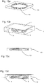
- the reference numeral 1 refers to the entire charging unit or charging arrangement (or the primary module).
- This has a housing 14 in which a primary coil 12, which also serves as a charging coil serves, is arranged.
- the reference numeral 100 denotes the secondary part, which has a secondary coil 120. This secondary part may be part of a motor vehicle, for example.
- the detection device 20 is shown. This is arranged here above the primary coil 12 and thus preferably between the primary coil 12 and the further coil 120 and the secondary module 100 which serves to charge the device to be charged (such as a vehicle).
- FIG. 13b shows a side view of in FIG. 13a shown illustration.
- the reference numeral 56 denotes a control means which controls the primary coil in response to a signal output from the detection means 20. For example, if the evaluation device 30 outputs a signal indicative of a foreign body between the primary coil 12 and the object, the controller may cause a shutdown of the primary coil.
- the detection device 20 or the sensor print here has the networks to be measured and is a flat design of several adjacent coils, as shown in the above-mentioned figures.
- This sensor device 40 is located near the surface in the base module and preferably directly opposite the primary coil.
- the associated measuring electronics can also be accommodated in this print or represent a separate print unit, which preferably also contacts the sensor print by means of a cable.
- the sensor device is able to monitor the surface of the floor module (or the gap between the primary module and secondary module) for objects.
- circuits e.g., trimming capacitors or capacitance diodes or potentiometers. This opens up possibilities for further applications. For example, an adjustment under different environmental conditions, such as a temperature compensation, take place. In addition, the sensitivity could be maintained and it could be discriminated against.
Landscapes
- Engineering & Computer Science (AREA)
- Power Engineering (AREA)
- Transportation (AREA)
- Mechanical Engineering (AREA)
- Charge And Discharge Circuits For Batteries Or The Like (AREA)
Applications Claiming Priority (1)
| Application Number | Priority Date | Filing Date | Title |
|---|---|---|---|
| DE102018109093.5A DE102018109093A1 (de) | 2018-04-17 | 2018-04-17 | Vorrichtung und Verfahren zur Kalibrierung von Objekterfassungseinrichtungen |
Publications (1)
| Publication Number | Publication Date |
|---|---|
| EP3556600A1 true EP3556600A1 (fr) | 2019-10-23 |
Family
ID=66217907
Family Applications (1)
| Application Number | Title | Priority Date | Filing Date |
|---|---|---|---|
| EP19169790.3A Pending EP3556600A1 (fr) | 2018-04-17 | 2019-04-17 | Dispositif et procédé d'étalonnage de dispositifs de détection d'objets |
Country Status (2)
| Country | Link |
|---|---|
| EP (1) | EP3556600A1 (fr) |
| DE (1) | DE102018109093A1 (fr) |
Cited By (1)
| Publication number | Priority date | Publication date | Assignee | Title |
|---|---|---|---|---|
| CN111090119A (zh) * | 2020-01-04 | 2020-05-01 | 北京有感科技有限责任公司 | 异物检测系统 |
Families Citing this family (1)
| Publication number | Priority date | Publication date | Assignee | Title |
|---|---|---|---|---|
| JP2022114397A (ja) * | 2021-01-26 | 2022-08-05 | Tdk株式会社 | 物体検出装置、送電装置、及び、電力伝送システム |
Citations (4)
| Publication number | Priority date | Publication date | Assignee | Title |
|---|---|---|---|---|
| US20150323694A1 (en) * | 2014-05-07 | 2015-11-12 | Witricity Corporation | Foreign object detection in wireless energy transfer systems |
| US20160187519A1 (en) * | 2014-12-30 | 2016-06-30 | Qualcomm Incorporated | Systems, methods, and apparatus for detecting ferromagnetic foreign objects in a predetermined space |
| US20170141622A1 (en) * | 2015-10-19 | 2017-05-18 | Witricity Corporation | Foreign Object Detection In Wireless Energy Transfer Systems |
| WO2017174380A1 (fr) * | 2016-04-06 | 2017-10-12 | Koninklijke Philips N.V. | Détection d'objet dans un système de transfert de puissance sans fil |
Family Cites Families (2)
| Publication number | Priority date | Publication date | Assignee | Title |
|---|---|---|---|---|
| US8258777B2 (en) * | 2009-09-04 | 2012-09-04 | Weihua Chen | Inductive proximity sensor |
| CN107005090B (zh) * | 2014-12-11 | 2020-08-25 | 皇家飞利浦有限公司 | 一种用于无线功率传送系统的装置和方法 |
-
2018
- 2018-04-17 DE DE102018109093.5A patent/DE102018109093A1/de active Pending
-
2019
- 2019-04-17 EP EP19169790.3A patent/EP3556600A1/fr active Pending
Patent Citations (4)
| Publication number | Priority date | Publication date | Assignee | Title |
|---|---|---|---|---|
| US20150323694A1 (en) * | 2014-05-07 | 2015-11-12 | Witricity Corporation | Foreign object detection in wireless energy transfer systems |
| US20160187519A1 (en) * | 2014-12-30 | 2016-06-30 | Qualcomm Incorporated | Systems, methods, and apparatus for detecting ferromagnetic foreign objects in a predetermined space |
| US20170141622A1 (en) * | 2015-10-19 | 2017-05-18 | Witricity Corporation | Foreign Object Detection In Wireless Energy Transfer Systems |
| WO2017174380A1 (fr) * | 2016-04-06 | 2017-10-12 | Koninklijke Philips N.V. | Détection d'objet dans un système de transfert de puissance sans fil |
Cited By (1)
| Publication number | Priority date | Publication date | Assignee | Title |
|---|---|---|---|---|
| CN111090119A (zh) * | 2020-01-04 | 2020-05-01 | 北京有感科技有限责任公司 | 异物检测系统 |
Also Published As
| Publication number | Publication date |
|---|---|
| DE102018109093A1 (de) | 2019-10-17 |
Similar Documents
| Publication | Publication Date | Title |
|---|---|---|
| DE102007046483B4 (de) | Schaltungsanordnung und Verfahren zur Überwachung einer elektrischen Isolation | |
| DE112013006074B4 (de) | Kapazitiver Sensor, der dafür ausgelegt ist, ein Heizelement als Antennenelektrode zu verwenden | |
| EP3124314B1 (fr) | Detection de corps etrangers, en particulier pour systemes de charge inductifs | |
| EP2100101B1 (fr) | Système pour mesurer une grandeur physique | |
| EP3028053B1 (fr) | Dispositif de détection de proportions de courant alternatif dans un circuit à courant continu et utilisation dudit dispositif | |
| DE60129529T2 (de) | Impedanzmessungsschaltkreis, -detektor und verfahren zur impedanzmessung | |
| WO2009074193A1 (fr) | Dispositif et procédé pour générer une impulsion de charge donnée en vue de réaliser une mesure de décharge partielle | |
| EP3631976B1 (fr) | Procédé servant à identifier un contact défectueux dans une installation photovoltaïque | |
| DE102010029762A1 (de) | Verfahren zur Bestimmung einer Restkopplung eines induktiven Leitfähigkeitssensors | |
| DE102013200871A1 (de) | Vorrichtung und Verfahren zur Diagnose eines kapazitiven Sensors | |
| DE102012008601A1 (de) | Kraftwagen und Verfahren zum Erkennen einer blockierten Schalteinrichtung einer Fahrzeugbatterie | |
| EP3788388B1 (fr) | Dispositif capteur et procédé de détermination d'une tension alternative | |
| DE10256064A1 (de) | Verfahren und Vorrichtung zur Bestimmung des Wassergehalts und der Leitfähigkeit in Böden und Schüttgütern | |
| WO2006034959A2 (fr) | Reglage, au niveau de la fabrication, d'un appareil de mesure pour une mesure de niveau capacitive et appareil de mesure correspondant | |
| EP2859374B1 (fr) | Dispositif pour calibrer un système de mesure de puissance pour des transformateurs de puissance | |
| DE112015005677T5 (de) | Erdschlusserfassungsvorrichtung für ein Fahrzeug | |
| DE112019000888T5 (de) | System zur Erdung und Diagnose | |
| DE102018109093A1 (de) | Vorrichtung und Verfahren zur Kalibrierung von Objekterfassungseinrichtungen | |
| DE102016208960B3 (de) | Überwachungsvorrichtung und Verfahren zum Überwachen einer gegenüber einem Referenzpotential galvanisch entkoppelten Wechselspannungsquelle | |
| WO2015036280A1 (fr) | Surveillance de l'isolation d'enroulements compensés en série d'un système de transmission d'énergie sans contact | |
| DE102008062659A1 (de) | Vorrichtung zur Diebstahl-Überwachung des Solargenerators einer PV-Anlage | |
| EP1151310A1 (fr) | Procede de mesure pour systeme de mesure capacitif | |
| EP3357742B1 (fr) | Dispositif de détection d'objets en particulier pour systèmes de charge | |
| DE112018004554T5 (de) | Batteriezellenüberwachungssystem | |
| DE10253864A1 (de) | Verfahren und Anordnung zur Erdschlussüberwachung eines Stators in Sternschaltung |
Legal Events
| Date | Code | Title | Description |
|---|---|---|---|
| PUAI | Public reference made under article 153(3) epc to a published international application that has entered the european phase |
Free format text: ORIGINAL CODE: 0009012 |
|
| STAA | Information on the status of an ep patent application or granted ep patent |
Free format text: STATUS: THE APPLICATION HAS BEEN PUBLISHED |
|
| AK | Designated contracting states |
Kind code of ref document: A1 Designated state(s): AL AT BE BG CH CY CZ DE DK EE ES FI FR GB GR HR HU IE IS IT LI LT LU LV MC MK MT NL NO PL PT RO RS SE SI SK SM TR |
|
| AX | Request for extension of the european patent |
Extension state: BA ME |
|
| STAA | Information on the status of an ep patent application or granted ep patent |
Free format text: STATUS: REQUEST FOR EXAMINATION WAS MADE |
|
| 17P | Request for examination filed |
Effective date: 20200417 |
|
| RBV | Designated contracting states (corrected) |
Designated state(s): AL AT BE BG CH CY CZ DE DK EE ES FI FR GB GR HR HU IE IS IT LI LT LU LV MC MK MT NL NO PL PT RO RS SE SI SK SM TR |
|
| STAA | Information on the status of an ep patent application or granted ep patent |
Free format text: STATUS: EXAMINATION IS IN PROGRESS |
|
| 17Q | First examination report despatched |
Effective date: 20210629 |