EP3563423B1 - Fotovoltaische verpackung und verfahren zur herstellung solch einer fotovoltaischen verpackung - Google Patents
Fotovoltaische verpackung und verfahren zur herstellung solch einer fotovoltaischen verpackung Download PDFInfo
- Publication number
- EP3563423B1 EP3563423B1 EP17818594.8A EP17818594A EP3563423B1 EP 3563423 B1 EP3563423 B1 EP 3563423B1 EP 17818594 A EP17818594 A EP 17818594A EP 3563423 B1 EP3563423 B1 EP 3563423B1
- Authority
- EP
- European Patent Office
- Prior art keywords
- photovoltaic
- photovoltaic cells
- packaging
- layer
- back layer
- Prior art date
- Legal status (The legal status is an assumption and is not a legal conclusion. Google has not performed a legal analysis and makes no representation as to the accuracy of the status listed.)
- Active
Links
Images





Classifications
-
- H—ELECTRICITY
- H10—SEMICONDUCTOR DEVICES; ELECTRIC SOLID-STATE DEVICES NOT OTHERWISE PROVIDED FOR
- H10F—INORGANIC SEMICONDUCTOR DEVICES SENSITIVE TO INFRARED RADIATION, LIGHT, ELECTROMAGNETIC RADIATION OF SHORTER WAVELENGTH OR CORPUSCULAR RADIATION
- H10F19/00—Integrated devices, or assemblies of multiple devices, comprising at least one photovoltaic cell covered by group H10F10/00, e.g. photovoltaic modules
- H10F19/80—Encapsulations or containers for integrated devices, or assemblies of multiple devices, having photovoltaic cells
- H10F19/85—Protective back sheets
-
- H—ELECTRICITY
- H10—SEMICONDUCTOR DEVICES; ELECTRIC SOLID-STATE DEVICES NOT OTHERWISE PROVIDED FOR
- H10F—INORGANIC SEMICONDUCTOR DEVICES SENSITIVE TO INFRARED RADIATION, LIGHT, ELECTROMAGNETIC RADIATION OF SHORTER WAVELENGTH OR CORPUSCULAR RADIATION
- H10F19/00—Integrated devices, or assemblies of multiple devices, comprising at least one photovoltaic cell covered by group H10F10/00, e.g. photovoltaic modules
- H10F19/80—Encapsulations or containers for integrated devices, or assemblies of multiple devices, having photovoltaic cells
-
- H—ELECTRICITY
- H10—SEMICONDUCTOR DEVICES; ELECTRIC SOLID-STATE DEVICES NOT OTHERWISE PROVIDED FOR
- H10F—INORGANIC SEMICONDUCTOR DEVICES SENSITIVE TO INFRARED RADIATION, LIGHT, ELECTROMAGNETIC RADIATION OF SHORTER WAVELENGTH OR CORPUSCULAR RADIATION
- H10F19/00—Integrated devices, or assemblies of multiple devices, comprising at least one photovoltaic cell covered by group H10F10/00, e.g. photovoltaic modules
- H10F19/90—Structures for connecting between photovoltaic cells, e.g. interconnections or insulating spacers
- H10F19/902—Structures for connecting between photovoltaic cells, e.g. interconnections or insulating spacers for series or parallel connection of photovoltaic cells
-
- H—ELECTRICITY
- H10—SEMICONDUCTOR DEVICES; ELECTRIC SOLID-STATE DEVICES NOT OTHERWISE PROVIDED FOR
- H10F—INORGANIC SEMICONDUCTOR DEVICES SENSITIVE TO INFRARED RADIATION, LIGHT, ELECTROMAGNETIC RADIATION OF SHORTER WAVELENGTH OR CORPUSCULAR RADIATION
- H10F71/00—Manufacture or treatment of devices covered by this subclass
- H10F71/137—Batch treatment of the devices
-
- Y—GENERAL TAGGING OF NEW TECHNOLOGICAL DEVELOPMENTS; GENERAL TAGGING OF CROSS-SECTIONAL TECHNOLOGIES SPANNING OVER SEVERAL SECTIONS OF THE IPC; TECHNICAL SUBJECTS COVERED BY FORMER USPC CROSS-REFERENCE ART COLLECTIONS [XRACs] AND DIGESTS
- Y02—TECHNOLOGIES OR APPLICATIONS FOR MITIGATION OR ADAPTATION AGAINST CLIMATE CHANGE
- Y02E—REDUCTION OF GREENHOUSE GAS [GHG] EMISSIONS, RELATED TO ENERGY GENERATION, TRANSMISSION OR DISTRIBUTION
- Y02E10/00—Energy generation through renewable energy sources
- Y02E10/50—Photovoltaic [PV] energy
Definitions
- the present teachings relate to a photovoltaic packaging having a plurality of electrically interconnected photovoltaic, or, solar, cells placed in between a front layer and a back layer.
- the present teachings also relate to a method for manufacturing such a photovoltaic packaging.
- FR 2 349 959 A1 relates to a solar panel and to a method of manufacturing of such a solar panel.
- An object of the invention is to provide a photovoltaic packaging which can be manufactured in an efficient manner at low costs, and which can be recycled in an efficient manner, to a large degree.
- the invention relates to a photovoltaic packaging, as defined in claim 1.
- a photovoltaic packaging comprising:
- the photovoltaic packaging according to the present teachings can be manufactured efficiently because lamination of encapsulant layers, which is time consuming and expensive, is no longer required. That means, according to the present invention the plurality of mutually connected photovoltaic cells may be located between the front layer and the back layer in the absence of any encapsulant layers.
- the packaging is free from encapsulant layers which encapsulate and fully embed photovoltaic cells, so that the front layer and the back layer are in direct contact with the plurality of photovoltaic cells.
- the front layer and the back layer may thus be connected directly to each other by means of the welded connection, along at least substantially the entire welded connection.
- Enclosing the plurality of photovoltaic cells between the polymer front and back layer by means of welding of said layers to each other is a very effective and cost efficient manner of protecting the photovoltaic cells from external influences like moisture and dust. Also, during recycling, the photovoltaic cells can easily be separated from the front and back layers, such as by cutting though said layers. Because each individual cell of the plurality of photovoltaic cells is separated from the remaining of the photovoltaic cells by the welded connection, each of the cells is positioned at a defined location, or, pocket, defined by the welded connection, between the front and back layers.
- Encapsulant layers are layers which encapsulate a photovoltaic cell, which fully embed the cell, and which may be melted or glued to it. Their function is to protect the photovoltaic cell.
- An encapsulant such as of ethylene-vinyl acetate (EVA) may have been provided in thin sheets placed on top of and underneath the solar cell. This sandwich has then been heated to 150 °C to polymerize the EVA and bond the encapsulant, the cell, and optionally also a front panel, or, top layer, and rear panel of a solar module together.
- EVA ethylene-vinyl acetate
- the welds mutually connecting the front and back layer are laser welds.
- one of the front layer and the back layer is laser transmissive, while the other of the front layer and the back layer is laser absorbent.
- the melting temperature of the front and back layer are similar, or at least the melting temperature range is overlapping.
- the laser welds preferably are discrete, linear. That is, the laser welded connection by means of which the front layer and the back layer are connected follows lines, that is, they are line-shaped.
- the front and back layer of the photovoltaic packaging are configured such that the plurality of photovoltaic cells do not adhere, or at most reversibly adhere, to either the front layer and the back layer.
- the photovoltaic, or, solar cells are commercially available solar cells such as wafer-based cells such as made of crystalline silicon.
- transparent to light is meant transparent to light to such an extent that in use of the photovoltaic packaging electrical power is generated by the plurality of photovoltaic cells due to incident sunlight.
- transparent to light is meant that the polymer front layer allows at least an average of 65%, preferably at least an average of 70%, more preferably at least an average of 75%, most preferably at least an average of 80% transmission of light in the wavelength range of 350 nm to 1200 nm as compared to a situation without the polymer front layer, when measuring the transmittance curves (full spectrum from 200-2500nm) using a Perkin Elmer Lambda 950 according to ASTM D1003 (used lamp: halogen in combination with deuterium lamp). That means that the transmission of light is measured according to ASTM D1003.
- each individual cell of the plurality of photovoltaic cells of the photovoltaic packaging is separated from the remaining of the photovoltaic cells by a continuous welded connection between the front layer and the back layer, the continuous welded connection extending around the individual cell, that means, around the perimeter of the individual cell.
- a continuous welded connection fully separates each of the cells from the remaining of the cells.
- the welded connection may comprise more than one weld passing between each two adjacent photovoltaic cells of the plurality of photovoltaic cells. This increases the reliability of the sealing, and thus protection, of the photovoltaic cells from the external influences as mentioned above.
- the polymer front layer may be a sheet having a thickness in the range of 20 to 1000 micrometer, preferably of 100 to 500 micrometer.
- the polymer back layer may be a sheet having a thickness in the range of 300 to 10000 micrometer, preferably of 300 to 3000 micrometer.
- the polymer of the front layer and/or of the back layer may be chosen from the group consisting of polyolefins, such as homopolymers (PP) or random copolymers (rPP) of polypropylene, for example a polymer prepared from propylene and ethylene monomore, for example from at least 90wt% propylene and at most 10 wt% ethylene; polyethylene (PE), e.g. linear low density polyethylene (LLDPE) or other polymers, such as polyethylene terephthalate (PET), polybutylene terephthalate (PBT), polycarbonates (PC), polymethylmethacrylate (PMMA), silicons and fluoroplastomers.
- the back layer may have a foamed core. Examples of materials that may be (laser) welded together include but are not limited to PP/rPP with PP, PET with PET, PET with PBT, LLDPE with PE, PC with PC and PMMA with PMMA.
- the polymer front layer is transparent to light.
- the polymer back layer may be prepared from a long glass fiber reinforced polypropylene, such as made by the process described in WO 2009/080281 , which disclosure is incorporated by reference.
- Pellets comprising a thermoplastic polymer sheath intimately surrounding glass filaments, which glass filaments are covered at least in part with an impregnating agent and extend in a longitudinal direction of said pellets, are for example commercially available under the brand name STAMAX.
- the front layer and/or the back layer may have an adhesive layer on their side facing the plurality of photovoltaic cells, wherein the composition of the adhesive of the adhesive layer is such that a self-adhesive effect is obtained after bringing the respective layer in contact with a photovoltaic cell, in such a manner that hardly any residual adhesive will remain behind on the photovoltaic cells, if at all, after removal of the respective layer from the photovoltaic cell.
- the front layer and/or the back layer thus reversibly adhere to the plurality of photovoltaic cells. In practice this can be accomplished by an adhesive that is known to the skilled person. The adhesive provides temporary adhesion until the respective layer is removed, which adhesive allows easy removal of the layer.
- Such an adhesive does not lose its adhesive strength, or at most to a limited degree, after a connection between two parts which has been effected by means of the adhesive in question is broken by separating the parts that have been joined together by means of the adhesive joint. Said adhesive remains behind on a first part, to which the adhesive had originally been applied. Because the adhesive does not lose its adhesive strength, or at most to a limited extent when the connection is broken, the adhesive can be reused for effecting an adhesive joint with the same second part of with another second part.
- the plurality of photovoltaic cells may be electrically connected to each other in a parallel electrical configuration, and alternatively in series configuration.
- the plurality of cells may be divided in various groups, wherein each cell of a group is connected in series to the other cells of that group, while groups may be connected in parallel, for example.
- the electrical conductors may be metal strips such as comprising copper, aluminium and/or silver. Alternatively the electrical conductors may be metal wires.
- the photovoltaic packaging according to the invention may further comprise a piece, such as a strip, of encapsulant extending over any electrical conductors between adjacent photovoltaic cells of the plurality of photovoltaic cells.
- the piece of encapsulant is heat-sealable, and may be sealingly connected to the conductors. This means that the front layer and the back layer are connected directly to each other by means of the welded connection, along substantially the entire welded connection.
- the packaging according to the invention may have a width, and may comprise a plurality of strips of encapsulant each extending in a continuous manner over the width of the photovoltaic packaging, between adjacent photovoltaic cells of the plurality of photovoltaic cells.
- the welded connection may extend over a strip and thus directly connect the front and the back layer together except for the, small, locations of the encapsulant strips where the front layer, strip material and back layer are welded to each other (the encapsulant strip separating the front layer and the back layer). This means that the front layer and the back layer are connected directly to each other by means of the welded connection, along substantially the entire welded connection.
- the packaging may have a plurality of elongate, wire-shaped, metal reinforcement elements, such as metal wires, preferably steel wires, incorporated within the back layer, distributed over the width of the back layer and extending along the length of the back layer.
- metal wires preferably steel wires
- Such a packaging is highly resistant to burning objects from the outside.
- the plurality of elongate metal reinforcement elements may provide sufficient protection against such objects passing through the packaging by melting the packaging material, in particular the front and back layer, or at least provide sufficient delay.
- the plurality of elongate metal reinforcement elements may be incorporated within the back layer by lamination, extrusion or injection moulding. Extrusion is preferred.
- the invention further relates to a method for manufacturing a photovoltaic packaging as defined in claim 13. According to the invention, a method for manufacturing a photovoltaic packaging is provided, the method comprising:
- the method further comprises the step of placing a piece, such as a strip, of encapsulant extending over any electrical conductors between adjacent photovoltaic cells of the plurality of photovoltaic cells, between the front layer and the back layer, and melting the piece of encapsulant to at least one of the front layer and the back layer.
- a piece such as a strip
- the invention also relates to a solar panel having a rigid, UV protective top layer which is transparent to light, such as a glass plate, connected to a photovoltaic packaging according to the invention on a front, sun facing side of the photovoltaic packaging.
- a solar panel having a rigid, UV protective top layer which is transparent to light, such as a glass plate, connected to a photovoltaic packaging according to the invention on a front, sun facing side of the photovoltaic packaging.
- the person skilled in the art knows how to increase the resistance to UV (decreased degradation of the material under the influence of sunlight) of materials, for example by adding UV stabilizers as are known in the art.
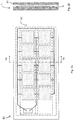
- FIG. 1a and 1b show a photovoltaic packaging 1 according to the present invention.
- the photovoltaic packaging 1 has ten photovoltaic cells, or, solar cells 3 in two parallel rows of five cells 3, while in practice the photovoltaic packaging may have less or (much) more solar cells such as a grid of six times ten solar cells.
- the solar cells 3 are mutually connected in an electrical manner by electrical conductors in the form of copper strips 2a, 2b, 2c.
- the strips 2a extend in the longitudinal direction of the packaging 1 while the strips 2b and 2c extend in the transverse direction.
- the main strips 2a extend between rows of solar cells 3 and are electrically connected to respective electrical contacts on the back side of each of the cells 3 by means of transverse strips 2b extending between a main strip 2a and an electrical contact of a solar cell 3.
- the ten cells 3 are in electrical connection in a parallel configuration while the two rows share a central longitudinal strip of the strips 2a, which may be the (-)-wire.
- the two outer strips of the strips 2a are connected by the transverse strip 2c and may be the (+)-wire.
- Such a parallel configuration may result in a higher durability as compared to the series configuration as shown in figure 4a (to be detailed below) because of the increased capability of the photovoltaic packaging 1 to deal with temperature differences between the copper strips 2a and the below described front and back sheets 6, 8.
- the transverse strips 2b may bend slightly in case that the solar cells 3 remain in place. This reduces the forces at, normally soldered, electrical connections between strips and solar cell contacts.
- conductors of other shapes may be used, such as wire-shaped conductors, i.e. conductive wires, such as of copper or aluminium.
- the rows of cells 3 thus formed may comprise a larger number of cells, such as ten cells.
- the panel may comprise a plurality of such rows, such as six rows.
- the above holds in an analogous manner for the further examples of packagings to be described below.
- the photovoltaic packaging 1 has a polymer back layer in the form of a back sheet 8 of polypropylene.
- the back sheet 8 has a thickness of 500 micrometer.
- the photovoltaic packaging also has a polymer front layer which is light transparent to such an extent that in use of the photovoltaic packaging 1 electrical power is generated by the plurality of photovoltaic cells 3 due to incident sunlight.
- the front layer is in the form of a front sheet 6 of polypropylene.
- the thickness of the front sheet 6 is 200 micrometer.
- the solar cells 3 are located between the front sheet 6 and back sheet 8 and do not adhere to either the front sheet 6 or the back sheet 8. Also, the front sheet 6 does not adhere to the back sheet 8, as visualized schematically in figure 1b .
- the front sheet 6 is connected locally to the back sheet 8 by means of laser welds 4 (indicated by dashed lines), i.e connected by means of laser welding.
- the photovoltaic packaging 1 has longitudinal welds 4 in the direction of the rows, on each side of each row, and transverse welds between each two adjacent cells 3, thereby creating ten pockets 9, one pocket 9 for each individual cell 3.
- laser welds 4 surround each individual solar cell 3 so that each cell 3 is enclosed in a pocket 9 defined by the front sheet 6 and back sheet 8 and one or more of the laser welds 4.
- a transverse connecting strip 2b from a cell 3 to a conductor strip 2a extends through a longitudinal weld 4.
- the (+)-wire and (-)-wires 2a can be connected to an external power cable via a junction box 12 which provides a sealed electrical external connection of the conductor strips 2a.
- Figure 1c shows in detail a junction of a longitudinal and a transverse weld 4.
- a circular weld part 4a may be provided.
- a photovoltaic packaging connecting element such as a screw 20 may safely be passed through the front 6 and back 8 sheets without compromising the full enclosure and thereby sealing from external influences such as moist and dust, of each cell 3 in its pocket 9.
- the packaging may be connected to a surrounding structure such as a supporting structure.
- FIGs 2a and 2b show a solar panel 50 according to the invention.
- the solar panel 50 comprises the photovoltaic packaging 1 of figures 1a-1c and a rigid, UV protective top layer which is transparent to light, in the form of a glass plate 51, connected to a top, sun facing side of the front sheet 6 by means of gluing the glass plate 51 to the front sheet 6, such as using an above-described "Post-it" adhesive.
- the glass plate 51 is of the same size, seen in plan view, as the front sheet 6 and back sheet 8.
- the solar panel 50 may additionally have a rigid further back layer in the form of a back plate connected to the back sheet, such as by means of gluing, for further strengthening of the solar panel.
- FIGs 3a and 3b show a photovoltaic packaging 101 which is to a large extent identical to the packaging 1 of figures 1a-1b .
- the photovoltaic packaging 101 has a front sheet 106 and a back sheet 108, in this example both made of polyethylene and having a thickness of 300 micrometer.
- Conductor strips 102a, 102b, 102c are provided to mutually connect the cells of the plurality of solar cells 103 in an electrical manner, like packaging 1.
- the front sheet 106 is connected locally to the back sheet 108 by means of laser welds 104.
- a laser weld 104, 104' extends continuously around each individual solar cell 103 so that each cell 103 is fully enclosed in a pocket 109 defined by the front sheet 106 and back sheet 108, as is the case with packaging 1.
- the difference is that each cell 103 of packaging 101 is completely surrounded by two welds, because two transverse welds 104' extend between each two adjacent cells 103 instead of one transverse weld in the packaging of figure 1a . for the remainder, the above description of packaging 1 applies in an analogous manner.
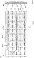
- FIG. 4a and 4b show a photovoltaic packaging 201 according to the present invention.
- the photovoltaic packaging 201 has ten photovoltaic, or, solar cells 203 in two parallel rows of five cells 203.
- the solar cells 203 are mutually connected in an electrical manner by electrical conductors in the form of copper strips 202a and 202d connected to respective electrical contacts on the back side of each of the cells.
- the strips 202a are mutually connected and may form a (+)-wire.
- the strips 202d are also mutually connected but are electrically isolated from the wires 202a and may form a (-)-wire. Both the (+)- and (-)-wire extend to a junction box 212 where they may be connected to an external power cable.
- the five cells 203 of each of the two rows are in electrical connection in a series configuration while the two rows are connected in parallel.
- the back layer 208, the front layer 206, and the pattern of welds 204, 204' is the same as in the packaging 101 of figure 3a-3b .
- conductor strips 202a and 202d pass through transverse welds 204'.
- a piece of encapsulant material 260 such as of EVA, is provided at the location of the pair of transverse welds 204', between the back layer 208 and the strip 202a and 202d of a row of cells 203.
- a piece of encapsulant material 260 is also provided between the front layer 206 and the same strips 202a and 202d, above the first-mentioned piece 260.
- the two pieces of encapsulant material 260 between which the strips 202a and 202d pass increase the sealing between two adjacent pockets 209.
- the two stacked pieces of encapsulant material 260 are melted to the front sheet 206 and back sheet 208 and to each other, while the strips 202a and 202b pass between them.
- a piece of encapsulant material may only be provided below, or alternatively on top of, the conductor strips. Such a piece thus connects to the front sheet 206 as well as to the back sheet 208.
- the photovoltaic packaging 301 of figures 5a and 5b is highly similar to packaging 201, except for the thickness of the back sheet, which may also be identical to the back sheet of packaging 201, and except for the embodiment of the encapsulant material.
- packaging 301 has strips 360 of encapsulant material, such as of EVA, extending in transverse direction between adjacent cells 303.
- the packaging 301 may be cut to length at the location of a transverse encapsulant strip 360, depending on the required number of cells 303 per row. In that case, a junction box, or at least an electrical connection, may be established with the conductor strips at the location of the cut.
- the strips 360 may extend over the entire width of the packaging.
- packaging 301 has a strip 360 on the top side of the conductor strips 302a and 302d only, that means between the front layer 306 and the strips 302a and 302d.
- the strip 360 is thus melted to the front sheet 306 as well as to the back sheet 308.
- two of such strips 360 may each time be provided between adjacent cells, similar to the two strips 260 of packaging 201.
- Figure 6a and 6b show a photovoltaic packaging 401 which is identical to packaging 1 except for the embodiment of the back sheet thereof.
- Packaging 401 has a back sheet 408 having a thickness of 400 micrometer.
- the back sheet 408 has five mutually parallel incorporated steel wires 415, for the purpose of reinforcing the back sheet 408.
- the back sheet 408 is made by co-extruding the wires 415 with the polymer of the back sheet. Alternatively the wires may be laminated between two sublayers of the back-sheet 408.
- the wires extend in the longitudinal direction of the packaging and less or more wires may be provided.
- the wires 415 are electrically isolated from conductor strips 402a-402c by the back sheet material.
- the wires 15 provide for an increased fire protection of any objects underneath the packaging in use.
- the wires 415 function as a safety net; the object may melt the front and back sheet of the packaging, but cannot pass through the wires 415.
- Such wires 415 may also be present in the other photovoltaic packagings according to the invention as described above.
- Figures 7a-7c show a part of a photovoltaic packaging 601 according to the invention, for the purpose of explaining an embodiment of a junction box 612 which may also be used in a similar manner in any of the packagings 1-401 according to the invention as described above.
- the junction box 612 is formed at a transverse end 613 of the packaging 601 and it comprises two halves 612a and 612b which are glued to the transverse end 613.
- Encapsulant material 660 is melted between the front and back sheet 606, 608 at the end 613, to increase the sealing of the packaging 601.
- Conductor strips 602a and 602d extend through the encapsulant material 660 to the junction box 612.
Landscapes
- Photovoltaic Devices (AREA)
Claims (15)
- Photovoltaikpaket (1; 101; 201; 301; 401; 601) umfassend:- eine Polymerrückseitenschicht (8),- eine Vielzahl von Photovoltaikzellen (3), die elektrisch mittels elektrischer Leiter miteinander verbunden sind,- eine Polymervorderseitenschicht (6), die für Licht transparent ist, und die ausgestaltet ist, um mittels Schweißen mit der Polymerrückseitenschicht verbunden zu werden,
wobei die Vielzahl von miteinander verbundenen Photovoltaikzellen sich zwischen der Vorderseitenschicht und der Rückseitenschicht befindet,
die Vorderseitenschicht (6) und die Rückseitenschicht (8) lokal mittels einer lokal geschweißten Verbindung (4) miteinander verbunden sind, so dass die Vielzahl der Photovoltaikzellen zwischen der Vorderseitenschicht und der Rückseitenschicht durch die geschweißte Verbindung, welche die Vielzahl der Photovoltaikzellen umgibt, vollständig umschlossen ist, und wobei jede individuelle Zelle der Vielzahl von Photovoltaikzellen von den restlichen Photovoltaikzellen durch die geschweißte Verbindung getrennt ist. - Photovoltaikpaket nach Anspruch 1, wobei die Vorderseitenschicht (6) und die Rückseitenschicht (8) mittels einer lasergeschweißten Verbindung lokal miteinander verbunden sind, wobei die Laserschwei-ßungen (4) vorzugsweise linienförmig sind.
- Photovoltaikpaket nach Anspruch 1 oder 2, wobei das Paket frei von Verkapselungsschichten ist, die Photovoltaikzellen (3) verkapseln und vollständig einbetten, so dass die Vorderseitenschicht (6) und die Rückseitenschicht (8) in direktem Kontakt mit der Vielzahl von Photovoltaikzellen sind.
- Photovoltaikpaket nach Anspruch 1, 2 oder 3, wobei die Vorderseitenschicht (6) und die Rückseitenschicht (8) so ausgestaltet sind, dass die Vielzahl von Photovoltaikzellen (3) nicht oder höchstens reversibel an der Vorderseitenschicht und/oder der Rückseitenschicht haftet.
- Photovoltaikpaket nach einem der vorhergehenden Ansprüche, wobei jede individuelle Zelle (3) von der Vielzahl von Photovoltaikzellen von den restlichen Photovoltaikzellen durch eine kontinuierliche lokale geschweißte Verbindung zwischen der Vorderseitenschicht und der Rückseitenschicht getrennt ist, wobei die kontinuierliche geschweißte Verbindung sich um die individuelle Zelle herum, das heißt um den Umfang der individuellen Zelle herum, erstreckt, wodurch eine Tasche (9) definiert wird, welche die individuelle Zelle (3) umschließt.
- Photovoltaikpaket (101) nach einem der vorhergehenden Ansprüche, wobei die geschweißte Verbindung mehr als eine Schweißung (104') umfasst, die zwischen jedweden zwei benachbarten Photovoltaikzellen (103) von der Vielzahl der Photovoltaikzellen hindurchführt.
- Photovoltaikpaket nach einem der vorhergehenden Ansprüche, wobei die Polymervorderseitenschicht (6) eine Lage mit einer Dicke im Bereich von 20 bis 1000 Mikrometern, vorzugsweise 100 bis 500 Mikrometern ist, und wobei die Polymerrückseitenschicht (8) eine Lage mit einer Dicke im Bereich von 300 bis 10000 Mikrometern, vorzugsweise 300 bis 3000 Mikrometern ist.
- Photovoltaikpaket nach einem der vorhergehenden Ansprüche, wobei die Polymervorderseitenschicht (6) und/oder die Polymerrückseitenschicht (8) ein Polymer ausgewählt aus der Gruppe bestehend aus Polyolefinen, wie Homopolymeren (PP) oder statistischen Copolymeren von Polypropylen (rPP), beispielsweise einem Polymer, das aus Propylen und Ethylenmonomer hergestellt ist, beispielsweise aus mindestens 90 Gew.% Propylen und höchstens 10 Gew.% Ethylen; Polyethylen, z. B. linearem Polyethylen mit niedriger Dichte (LLDPE), oder anderen Polymeren, wie Polyethylenterephthalat (PET), Polybutylenterephthalat (PBT), Polycarbonaten (PC), Polymethylmethacrylat (PMMA), Silikonen und Fluorplastomeren umfasst.
- Photovoltaikpaket nach einem der vorhergehenden Ansprüche, wobei die Vielzahl der Photovoltaikzellen (3) in einer parallelen elektrischen Konfiguration elektrisch miteinander verbunden ist.
- Photovoltaikpaket (201) nach einem der vorhergehenden Ansprüche, des Weiteren umfassend ein Stück, wie einen Streifen, Verkapselungsmittel (260), das sich über jegliche elektrischen Leiter (202a, 202d) zwischen benachbarten Photovoltaikzellen (203) von der Vielzahl der Photovoltaikzellen erstreckt.
- Photovoltaikpaket (301) nach Anspruch 10 mit einer Breite und umfassend eine Vielzahl der Streifen des Verkapselungsmittels (360), die sich jeweils in einer kontinuierlichen Weise über die Breite des Photovoltaikpakets zwischen benachbarten Photovoltaikzellen (303) von der Vielzahl der Photovoltaikzellen erstrecken,
wobei die geschweißte Verbindung vorzugsweise eine kontinuierliche Schweißung direkt benachbart zu jedem Verkapselungsstreifen auf jeder von dessen Seiten umfasst. - Photovoltaikpaket (401) nach einem der vorhergehenden Ansprüche mit einer Vielzahl von Metallverstärkungselementen, wie Stahldrähten (415), die in die Rückseitenschicht (408) eingearbeitet sind, über die Breite der Rückseitenschicht verteilt sind und sich entlang der Länge der Rückseitenschicht erstrecken.
- Verfahren zum Fertigen eines Photovoltaikpakets (1; 101; 201; 301; 401; 601) nach einem der vorhergehenden Ansprüche, umfassend:- Bereitstellen einer Polymervorderseitenschicht (6) und einer Polymerrückseitenschicht (8),- Bereitstellen einer Vielzahl von Photovoltaikzellen (3), die elektrisch miteinander verbunden sind,- Platzieren der Vielzahl von Photovoltaikzellen zwischen der Vorderseitenschicht und der Rückseitenschicht,- lokales Verschweißen der Vorderseitenschicht und der Rückseitenschicht miteinander, so dass die Vielzahl der Photovoltaikzellen zwischen der Vorderseitenschicht und der Rückseitenschicht durch die lokal geschweißte Verbindung (4), welche die Vielzahl der Photovoltaikzellen umgibt, vollständig umschlossen ist, und wobei jede individuelle Zelle der Vielzahl von Photovoltaikzellen von den restlichen Photovoltaikzellen durch die geschweißte Verbindung getrennt ist.
- Verfahren nach Anspruch 13, des Weiteren umfassend den Schritt des Platzierens eines Stücks, wie eines Streifens, von Verkapselungsmittel (260; 360), so dass sich dieses über jegliche elektrischen Leiter zwischen benachbarten Photovoltaikzellen von der Vielzahl von Photovoltaikzellen zwischen der Vorderseitenschicht und der Rückseitenschicht erstreckt, und Schmelzen des Stücks des Verkapselungsmittels an mindestens eine von der Vorderseitenschicht und der Rückseitenschicht.
- Solarkollektor (50) mit einer steifen, UV-schützenden Deckschicht, die für Licht transparent ist, wie einer Glasplatte (51), die mit einem Photovoltaikpaket (1) nach einem der vorhergehenden Ansprüche 1 bis 12 an einer vorderen, zur Sonne weisenden Seite des Photovoltaikpakets verbunden ist.
Applications Claiming Priority (2)
| Application Number | Priority Date | Filing Date | Title |
|---|---|---|---|
| EP17150032 | 2017-01-02 | ||
| PCT/EP2017/084537 WO2018122203A1 (en) | 2017-01-02 | 2017-12-22 | A photovoltaic packaging, and a method for manufacturing such a photovoltaic packaging |
Publications (2)
| Publication Number | Publication Date |
|---|---|
| EP3563423A1 EP3563423A1 (de) | 2019-11-06 |
| EP3563423B1 true EP3563423B1 (de) | 2020-08-26 |
Family
ID=57681526
Family Applications (1)
| Application Number | Title | Priority Date | Filing Date |
|---|---|---|---|
| EP17818594.8A Active EP3563423B1 (de) | 2017-01-02 | 2017-12-22 | Fotovoltaische verpackung und verfahren zur herstellung solch einer fotovoltaischen verpackung |
Country Status (4)
| Country | Link |
|---|---|
| US (2) | US12446330B2 (de) |
| EP (1) | EP3563423B1 (de) |
| CN (1) | CN110326120B (de) |
| WO (1) | WO2018122203A1 (de) |
Families Citing this family (3)
| Publication number | Priority date | Publication date | Assignee | Title |
|---|---|---|---|---|
| NL2022468B1 (en) * | 2019-01-29 | 2020-08-18 | Solarge B V | [photovotaic panel] |
| CN114424349B (zh) * | 2019-09-19 | 2024-05-28 | Sabic环球技术有限责任公司 | 光伏元件 |
| EP4228010A4 (de) * | 2020-12-30 | 2024-05-29 | Risen Energy Co. Ltd | Verpackungsverfahren für ein solarzellenmodul, verbindungsverfahren für einen solarzellenstrang, solarzellenmodul und herstellungsverfahren dafür |
Family Cites Families (30)
| Publication number | Priority date | Publication date | Assignee | Title |
|---|---|---|---|---|
| DE2445642C2 (de) * | 1974-09-25 | 1982-05-27 | Licentia Patent-Verwaltungs-Gmbh, 6000 Frankfurt | Solarzellenanordnung |
| JPS52129295A (en) * | 1976-04-23 | 1977-10-29 | Agency Of Ind Science & Technol | Solar battery device and its production |
| FR2349959A1 (fr) * | 1976-04-27 | 1977-11-25 | Radiotechnique Compelec | Procede de fabrication de panneaux de photopiles solaires et panneaux fabriques par ce procede |
| JPS604270A (ja) * | 1983-06-22 | 1985-01-10 | Hitachi Ltd | 太陽電池の製造方法 |
| JPS60214550A (ja) | 1984-04-10 | 1985-10-26 | Nippon Denso Co Ltd | 太陽電池モジユ−ル |
| EP0631328B1 (de) * | 1993-06-24 | 1998-05-27 | Canon Kabushiki Kaisha | Solarmodul mit warm-verschweisstem Teil zur Verbesserung der Feuchtigkeitsbeständigkeit |
| US5437735A (en) * | 1993-12-30 | 1995-08-01 | United Solar Systems Corporation | Photovoltaic shingle system |
| US5575861A (en) * | 1993-12-30 | 1996-11-19 | United Solar Systems Corporation | Photovoltaic shingle system |
| US6459032B1 (en) * | 1995-05-15 | 2002-10-01 | Daniel Luch | Substrate structures for integrated series connected photovoltaic arrays and process of manufacture of such arrays |
| JP3972233B2 (ja) * | 1999-09-02 | 2007-09-05 | 富士電機ホールディングス株式会社 | 太陽電池モジュール |
| JP4480106B2 (ja) * | 2000-05-16 | 2010-06-16 | 大日本印刷株式会社 | 太陽電池モジュ−ル |
| JP2002237606A (ja) * | 2000-12-04 | 2002-08-23 | Canon Inc | 太陽電池用基板、それを用いた太陽電池及び太陽電池の製造方法 |
| US7098395B2 (en) * | 2001-03-29 | 2006-08-29 | Kaneka Corporation | Thin-film solar cell module of see-through type |
| EP2251911B1 (de) * | 2002-10-25 | 2017-11-29 | Nakajima Glass Co., Inc. | Solarzellen Modul Herstellungsverfahren |
| EP1959502A1 (de) * | 2007-02-14 | 2008-08-20 | Imphy Alloys | Photovoltaikmodul und Module zur Energie- oder Lichterzeugung |
| US20090000222A1 (en) * | 2007-06-28 | 2009-01-01 | Kalkanoglu Husnu M | Photovoltaic Roofing Tiles And Methods For Making Them |
| ES2376076T3 (es) | 2007-12-21 | 2012-03-08 | Saudi Basic Industries Corporation | Procedimiento para producir composiciones termopl�?sticas reforzadas con fibra de vidrio larga. |
| EP2250679A2 (de) * | 2008-02-02 | 2010-11-17 | RENOLIT Belgium N.V. | Photovoltaische module und verfahren zu ihrer herstellung |
| US20120138117A1 (en) * | 2008-03-20 | 2012-06-07 | Miasole | Thermoplastic wire network support for photovoltaic cells |
| US20120085391A1 (en) | 2010-10-06 | 2012-04-12 | Uday Varde | Structure and method for mounting a photovoltaic material |
| EP2629339B1 (de) | 2012-02-17 | 2015-04-15 | Eppstein Technologies GmbH | Foliensystem zur Kontaktierung von Photovoltaik-Zellen |
| FR2988222B1 (fr) | 2012-03-13 | 2016-06-24 | Commissariat Energie Atomique | Module photovoltaique comprenant des elements de conversion spectrale localises et procede de realisation |
| JP2013252667A (ja) * | 2012-06-07 | 2013-12-19 | Omron Corp | 樹脂部品、光電センサおよび樹脂部品の製造方法 |
| JP6011050B2 (ja) * | 2012-06-15 | 2016-10-19 | Jnc株式会社 | 太陽電池用封止材 |
| WO2014071417A2 (en) * | 2012-11-05 | 2014-05-08 | Solexel, Inc. | Systems and methods for monolithically isled solar photovoltaic cells and modules |
| CN203774347U (zh) * | 2013-12-27 | 2014-08-13 | 比亚迪股份有限公司 | 光伏电池组件 |
| ES2745557T3 (es) * | 2014-03-07 | 2020-03-02 | Saudi Basic Ind Corp | Cubierta de tejado modular |
| US20150263196A1 (en) | 2014-03-13 | 2015-09-17 | E I Du Pont De Nemours And Company | Photovoltaic module and process for manufacture thereof |
| US20160351740A1 (en) | 2015-05-28 | 2016-12-01 | Kyocera Corporation | Solar cell module and solar cell device |
| JP7291380B2 (ja) | 2018-06-08 | 2023-06-15 | 株式会社古川リサーチオフィス | 鼻水又は鼻づまりの口腔粘膜投与用即効性改善剤 |
-
2017
- 2017-12-22 EP EP17818594.8A patent/EP3563423B1/de active Active
- 2017-12-22 WO PCT/EP2017/084537 patent/WO2018122203A1/en not_active Ceased
- 2017-12-22 US US16/474,181 patent/US12446330B2/en active Active
- 2017-12-22 CN CN201780087176.7A patent/CN110326120B/zh active Active
-
2024
- 2024-09-23 US US18/893,125 patent/US20250015217A1/en active Pending
Non-Patent Citations (1)
| Title |
|---|
| None * |
Also Published As
| Publication number | Publication date |
|---|---|
| WO2018122203A1 (en) | 2018-07-05 |
| CN110326120A (zh) | 2019-10-11 |
| US20250015217A1 (en) | 2025-01-09 |
| CN110326120B (zh) | 2022-11-11 |
| US20210305445A1 (en) | 2021-09-30 |
| US12446330B2 (en) | 2025-10-14 |
| EP3563423A1 (de) | 2019-11-06 |
Similar Documents
| Publication | Publication Date | Title |
|---|---|---|
| US20250015217A1 (en) | Photovoltaic packaging, and a method for manufacturing such a photovoltaic packaging | |
| US5733382A (en) | Solar cell modules and method of making same | |
| KR101985053B1 (ko) | 광 지향 매체를 포함하는 광기전 모듈 및 이를 제조하는 방법 | |
| CN114424349B (zh) | 光伏元件 | |
| US20160254404A1 (en) | Photovoltaic panel and method for producing same | |
| JP7317479B2 (ja) | 太陽電池モジュールおよび太陽電池モジュールの製造方法 | |
| KR102607102B1 (ko) | 태양광모듈, 태양광 봉합재 및 태양광모듈의 제조방법 | |
| US8497153B2 (en) | Integrated back-sheet for back contact photovoltaic module | |
| US20140130841A1 (en) | Solar module and manufacturing method therefor | |
| WO2013066813A1 (en) | Integrated back-sheet for back contact photovoltaic module | |
| US20130160813A1 (en) | Back contact photovoltaic module with integrated circuitry | |
| TW201526266A (zh) | 用於傳送可撓性太陽能電池至捲對捲模組裝配製程之方法 | |
| WO2013066815A1 (en) | Solar cell module and process for making the same | |
| US20160372618A1 (en) | Solar Cell Strip Assembly and Method of Making | |
| CN110337728B (zh) | 太阳能电池模块及太阳能电池模块的制造方法 | |
| US20130104959A1 (en) | Integrated back-sheet for back contact photovoltaic module | |
| EP2824715B1 (de) | Solarzellenmodul und verfahren zur herstellung davon | |
| US20130104960A1 (en) | Integrated back-sheet for back contact photovoltaic module | |
| EP2824718A1 (de) | Fotovoltaisches Modul und Herstellungsverfahren | |
| US20180309002A1 (en) | Solar cell protective sheet, method for producing same, solar cell module, and method for producing same | |
| US10950745B2 (en) | Manufacturing systems and methods including inline cutting | |
| WO2011152350A1 (ja) | 太陽電池モジュールの製造方法 | |
| US20130104958A1 (en) | Integrated back-sheet for back contact photovoltaic module | |
| KR101220113B1 (ko) | 내습용 태양전지모듈 및 태양전지모듈의 제조방법 | |
| KR102885769B1 (ko) | 건물 일체형 태양광 모듈 |
Legal Events
| Date | Code | Title | Description |
|---|---|---|---|
| STAA | Information on the status of an ep patent application or granted ep patent |
Free format text: STATUS: UNKNOWN |
|
| STAA | Information on the status of an ep patent application or granted ep patent |
Free format text: STATUS: THE INTERNATIONAL PUBLICATION HAS BEEN MADE |
|
| PUAI | Public reference made under article 153(3) epc to a published international application that has entered the european phase |
Free format text: ORIGINAL CODE: 0009012 |
|
| STAA | Information on the status of an ep patent application or granted ep patent |
Free format text: STATUS: REQUEST FOR EXAMINATION WAS MADE |
|
| 17P | Request for examination filed |
Effective date: 20190620 |
|
| AK | Designated contracting states |
Kind code of ref document: A1 Designated state(s): AL AT BE BG CH CY CZ DE DK EE ES FI FR GB GR HR HU IE IS IT LI LT LU LV MC MK MT NL NO PL PT RO RS SE SI SK SM TR |
|
| AX | Request for extension of the european patent |
Extension state: BA ME |
|
| DAV | Request for validation of the european patent (deleted) | ||
| DAX | Request for extension of the european patent (deleted) | ||
| GRAP | Despatch of communication of intention to grant a patent |
Free format text: ORIGINAL CODE: EPIDOSNIGR1 |
|
| STAA | Information on the status of an ep patent application or granted ep patent |
Free format text: STATUS: GRANT OF PATENT IS INTENDED |
|
| INTG | Intention to grant announced |
Effective date: 20200430 |
|
| GRAS | Grant fee paid |
Free format text: ORIGINAL CODE: EPIDOSNIGR3 |
|
| GRAA | (expected) grant |
Free format text: ORIGINAL CODE: 0009210 |
|
| STAA | Information on the status of an ep patent application or granted ep patent |
Free format text: STATUS: THE PATENT HAS BEEN GRANTED |
|
| AK | Designated contracting states |
Kind code of ref document: B1 Designated state(s): AL AT BE BG CH CY CZ DE DK EE ES FI FR GB GR HR HU IE IS IT LI LT LU LV MC MK MT NL NO PL PT RO RS SE SI SK SM TR |
|
| REG | Reference to a national code |
Ref country code: GB Ref legal event code: FG4D |
|
| REG | Reference to a national code |
Ref country code: CH Ref legal event code: EP |
|
| REG | Reference to a national code |
Ref country code: AT Ref legal event code: REF Ref document number: 1307219 Country of ref document: AT Kind code of ref document: T Effective date: 20200915 |
|
| REG | Reference to a national code |
Ref country code: IE Ref legal event code: FG4D |
|
| REG | Reference to a national code |
Ref country code: DE Ref legal event code: R096 Ref document number: 602017022518 Country of ref document: DE |
|
| REG | Reference to a national code |
Ref country code: NL Ref legal event code: FP |
|
| REG | Reference to a national code |
Ref country code: LT Ref legal event code: MG4D |
|
| PG25 | Lapsed in a contracting state [announced via postgrant information from national office to epo] |
Ref country code: HR Free format text: LAPSE BECAUSE OF FAILURE TO SUBMIT A TRANSLATION OF THE DESCRIPTION OR TO PAY THE FEE WITHIN THE PRESCRIBED TIME-LIMIT Effective date: 20200826 Ref country code: LT Free format text: LAPSE BECAUSE OF FAILURE TO SUBMIT A TRANSLATION OF THE DESCRIPTION OR TO PAY THE FEE WITHIN THE PRESCRIBED TIME-LIMIT Effective date: 20200826 Ref country code: GR Free format text: LAPSE BECAUSE OF FAILURE TO SUBMIT A TRANSLATION OF THE DESCRIPTION OR TO PAY THE FEE WITHIN THE PRESCRIBED TIME-LIMIT Effective date: 20201127 Ref country code: NO Free format text: LAPSE BECAUSE OF FAILURE TO SUBMIT A TRANSLATION OF THE DESCRIPTION OR TO PAY THE FEE WITHIN THE PRESCRIBED TIME-LIMIT Effective date: 20201126 Ref country code: BG Free format text: LAPSE BECAUSE OF FAILURE TO SUBMIT A TRANSLATION OF THE DESCRIPTION OR TO PAY THE FEE WITHIN THE PRESCRIBED TIME-LIMIT Effective date: 20201126 Ref country code: FI Free format text: LAPSE BECAUSE OF FAILURE TO SUBMIT A TRANSLATION OF THE DESCRIPTION OR TO PAY THE FEE WITHIN THE PRESCRIBED TIME-LIMIT Effective date: 20200826 Ref country code: PT Free format text: LAPSE BECAUSE OF FAILURE TO SUBMIT A TRANSLATION OF THE DESCRIPTION OR TO PAY THE FEE WITHIN THE PRESCRIBED TIME-LIMIT Effective date: 20201228 Ref country code: SE Free format text: LAPSE BECAUSE OF FAILURE TO SUBMIT A TRANSLATION OF THE DESCRIPTION OR TO PAY THE FEE WITHIN THE PRESCRIBED TIME-LIMIT Effective date: 20200826 |
|
| REG | Reference to a national code |
Ref country code: AT Ref legal event code: MK05 Ref document number: 1307219 Country of ref document: AT Kind code of ref document: T Effective date: 20200826 |
|
| PG25 | Lapsed in a contracting state [announced via postgrant information from national office to epo] |
Ref country code: RS Free format text: LAPSE BECAUSE OF FAILURE TO SUBMIT A TRANSLATION OF THE DESCRIPTION OR TO PAY THE FEE WITHIN THE PRESCRIBED TIME-LIMIT Effective date: 20200826 Ref country code: LV Free format text: LAPSE BECAUSE OF FAILURE TO SUBMIT A TRANSLATION OF THE DESCRIPTION OR TO PAY THE FEE WITHIN THE PRESCRIBED TIME-LIMIT Effective date: 20200826 Ref country code: PL Free format text: LAPSE BECAUSE OF FAILURE TO SUBMIT A TRANSLATION OF THE DESCRIPTION OR TO PAY THE FEE WITHIN THE PRESCRIBED TIME-LIMIT Effective date: 20200826 Ref country code: IS Free format text: LAPSE BECAUSE OF FAILURE TO SUBMIT A TRANSLATION OF THE DESCRIPTION OR TO PAY THE FEE WITHIN THE PRESCRIBED TIME-LIMIT Effective date: 20201226 |
|
| PG25 | Lapsed in a contracting state [announced via postgrant information from national office to epo] |
Ref country code: EE Free format text: LAPSE BECAUSE OF FAILURE TO SUBMIT A TRANSLATION OF THE DESCRIPTION OR TO PAY THE FEE WITHIN THE PRESCRIBED TIME-LIMIT Effective date: 20200826 Ref country code: RO Free format text: LAPSE BECAUSE OF FAILURE TO SUBMIT A TRANSLATION OF THE DESCRIPTION OR TO PAY THE FEE WITHIN THE PRESCRIBED TIME-LIMIT Effective date: 20200826 Ref country code: DK Free format text: LAPSE BECAUSE OF FAILURE TO SUBMIT A TRANSLATION OF THE DESCRIPTION OR TO PAY THE FEE WITHIN THE PRESCRIBED TIME-LIMIT Effective date: 20200826 Ref country code: CZ Free format text: LAPSE BECAUSE OF FAILURE TO SUBMIT A TRANSLATION OF THE DESCRIPTION OR TO PAY THE FEE WITHIN THE PRESCRIBED TIME-LIMIT Effective date: 20200826 Ref country code: SM Free format text: LAPSE BECAUSE OF FAILURE TO SUBMIT A TRANSLATION OF THE DESCRIPTION OR TO PAY THE FEE WITHIN THE PRESCRIBED TIME-LIMIT Effective date: 20200826 |
|
| REG | Reference to a national code |
Ref country code: DE Ref legal event code: R097 Ref document number: 602017022518 Country of ref document: DE |
|
| PG25 | Lapsed in a contracting state [announced via postgrant information from national office to epo] |
Ref country code: ES Free format text: LAPSE BECAUSE OF FAILURE TO SUBMIT A TRANSLATION OF THE DESCRIPTION OR TO PAY THE FEE WITHIN THE PRESCRIBED TIME-LIMIT Effective date: 20200826 Ref country code: AT Free format text: LAPSE BECAUSE OF FAILURE TO SUBMIT A TRANSLATION OF THE DESCRIPTION OR TO PAY THE FEE WITHIN THE PRESCRIBED TIME-LIMIT Effective date: 20200826 Ref country code: AL Free format text: LAPSE BECAUSE OF FAILURE TO SUBMIT A TRANSLATION OF THE DESCRIPTION OR TO PAY THE FEE WITHIN THE PRESCRIBED TIME-LIMIT Effective date: 20200826 |
|
| PG25 | Lapsed in a contracting state [announced via postgrant information from national office to epo] |
Ref country code: SK Free format text: LAPSE BECAUSE OF FAILURE TO SUBMIT A TRANSLATION OF THE DESCRIPTION OR TO PAY THE FEE WITHIN THE PRESCRIBED TIME-LIMIT Effective date: 20200826 |
|
| PLBE | No opposition filed within time limit |
Free format text: ORIGINAL CODE: 0009261 |
|
| STAA | Information on the status of an ep patent application or granted ep patent |
Free format text: STATUS: NO OPPOSITION FILED WITHIN TIME LIMIT |
|
| PG25 | Lapsed in a contracting state [announced via postgrant information from national office to epo] |
Ref country code: IT Free format text: LAPSE BECAUSE OF FAILURE TO SUBMIT A TRANSLATION OF THE DESCRIPTION OR TO PAY THE FEE WITHIN THE PRESCRIBED TIME-LIMIT Effective date: 20200826 |
|
| REG | Reference to a national code |
Ref country code: CH Ref legal event code: PL |
|
| 26N | No opposition filed |
Effective date: 20210527 |
|
| PG25 | Lapsed in a contracting state [announced via postgrant information from national office to epo] |
Ref country code: MC Free format text: LAPSE BECAUSE OF FAILURE TO SUBMIT A TRANSLATION OF THE DESCRIPTION OR TO PAY THE FEE WITHIN THE PRESCRIBED TIME-LIMIT Effective date: 20200826 |
|
| PG25 | Lapsed in a contracting state [announced via postgrant information from national office to epo] |
Ref country code: LU Free format text: LAPSE BECAUSE OF NON-PAYMENT OF DUE FEES Effective date: 20201222 Ref country code: IE Free format text: LAPSE BECAUSE OF NON-PAYMENT OF DUE FEES Effective date: 20201222 |
|
| PG25 | Lapsed in a contracting state [announced via postgrant information from national office to epo] |
Ref country code: CH Free format text: LAPSE BECAUSE OF NON-PAYMENT OF DUE FEES Effective date: 20201231 Ref country code: LI Free format text: LAPSE BECAUSE OF NON-PAYMENT OF DUE FEES Effective date: 20201231 |
|
| PG25 | Lapsed in a contracting state [announced via postgrant information from national office to epo] |
Ref country code: TR Free format text: LAPSE BECAUSE OF FAILURE TO SUBMIT A TRANSLATION OF THE DESCRIPTION OR TO PAY THE FEE WITHIN THE PRESCRIBED TIME-LIMIT Effective date: 20200826 Ref country code: MT Free format text: LAPSE BECAUSE OF FAILURE TO SUBMIT A TRANSLATION OF THE DESCRIPTION OR TO PAY THE FEE WITHIN THE PRESCRIBED TIME-LIMIT Effective date: 20200826 Ref country code: CY Free format text: LAPSE BECAUSE OF FAILURE TO SUBMIT A TRANSLATION OF THE DESCRIPTION OR TO PAY THE FEE WITHIN THE PRESCRIBED TIME-LIMIT Effective date: 20200826 |
|
| PG25 | Lapsed in a contracting state [announced via postgrant information from national office to epo] |
Ref country code: MK Free format text: LAPSE BECAUSE OF FAILURE TO SUBMIT A TRANSLATION OF THE DESCRIPTION OR TO PAY THE FEE WITHIN THE PRESCRIBED TIME-LIMIT Effective date: 20200826 |
|
| GBPC | Gb: european patent ceased through non-payment of renewal fee |
Effective date: 20211222 |
|
| PG25 | Lapsed in a contracting state [announced via postgrant information from national office to epo] |
Ref country code: GB Free format text: LAPSE BECAUSE OF NON-PAYMENT OF DUE FEES Effective date: 20211222 |
|
| P01 | Opt-out of the competence of the unified patent court (upc) registered |
Effective date: 20230529 |
|
| PG25 | Lapsed in a contracting state [announced via postgrant information from national office to epo] |
Ref country code: SI Free format text: LAPSE BECAUSE OF FAILURE TO SUBMIT A TRANSLATION OF THE DESCRIPTION OR TO PAY THE FEE WITHIN THE PRESCRIBED TIME-LIMIT Effective date: 20200826 |
|
| REG | Reference to a national code |
Ref country code: DE Ref legal event code: R079 Ref document number: 602017022518 Country of ref document: DE Free format text: PREVIOUS MAIN CLASS: H01L0031049000 Ipc: H10F0019850000 |
|
| PGFP | Annual fee paid to national office [announced via postgrant information from national office to epo] |
Ref country code: NL Payment date: 20251226 Year of fee payment: 9 Ref country code: FR Payment date: 20251226 Year of fee payment: 9 |
|
| PGFP | Annual fee paid to national office [announced via postgrant information from national office to epo] |
Ref country code: BE Payment date: 20251229 Year of fee payment: 9 |
|
| PGFP | Annual fee paid to national office [announced via postgrant information from national office to epo] |
Ref country code: DE Payment date: 20251229 Year of fee payment: 9 |