EP3568703B1 - Dispositif de microscopie à force atomique, procédé et système lithographique - Google Patents
Dispositif de microscopie à force atomique, procédé et système lithographique Download PDFInfo
- Publication number
- EP3568703B1 EP3568703B1 EP18702350.2A EP18702350A EP3568703B1 EP 3568703 B1 EP3568703 B1 EP 3568703B1 EP 18702350 A EP18702350 A EP 18702350A EP 3568703 B1 EP3568703 B1 EP 3568703B1
- Authority
- EP
- European Patent Office
- Prior art keywords
- signal
- sample
- probe
- probe tip
- atomic force
- Prior art date
- Legal status (The legal status is an assumption and is not a legal conclusion. Google has not performed a legal analysis and makes no representation as to the accuracy of the status listed.)
- Active
Links
Images



Classifications
-
- G—PHYSICS
- G01—MEASURING; TESTING
- G01Q—SCANNING-PROBE TECHNIQUES OR APPARATUS; APPLICATIONS OF SCANNING-PROBE TECHNIQUES, e.g. SCANNING PROBE MICROSCOPY [SPM]
- G01Q60/00—Particular types of SPM [Scanning Probe Microscopy] or microscopes; Essential components thereof
- G01Q60/24—AFM [Atomic Force Microscopy] or apparatus therefor, e.g. AFM probes
- G01Q60/30—Scanning potential microscopy
-
- G—PHYSICS
- G01—MEASURING; TESTING
- G01Q—SCANNING-PROBE TECHNIQUES OR APPARATUS; APPLICATIONS OF SCANNING-PROBE TECHNIQUES, e.g. SCANNING PROBE MICROSCOPY [SPM]
- G01Q60/00—Particular types of SPM [Scanning Probe Microscopy] or microscopes; Essential components thereof
- G01Q60/24—AFM [Atomic Force Microscopy] or apparatus therefor, e.g. AFM probes
- G01Q60/32—AC mode
-
- G—PHYSICS
- G01—MEASURING; TESTING
- G01N—INVESTIGATING OR ANALYSING MATERIALS BY DETERMINING THEIR CHEMICAL OR PHYSICAL PROPERTIES
- G01N29/00—Investigating or analysing materials by the use of ultrasonic, sonic or infrasonic waves; Visualisation of the interior of objects by transmitting ultrasonic or sonic waves through the object
- G01N29/04—Analysing solids
- G01N29/06—Visualisation of the interior, e.g. acoustic microscopy
- G01N29/0654—Imaging
- G01N29/0681—Imaging by acoustic microscopy, e.g. scanning acoustic microscopy
-
- G—PHYSICS
- G01—MEASURING; TESTING
- G01Q—SCANNING-PROBE TECHNIQUES OR APPARATUS; APPLICATIONS OF SCANNING-PROBE TECHNIQUES, e.g. SCANNING PROBE MICROSCOPY [SPM]
- G01Q10/00—Scanning or positioning arrangements, i.e. arrangements for actively controlling the movement or position of the probe
- G01Q10/04—Fine scanning or positioning
- G01Q10/06—Circuits or algorithms therefor
- G01Q10/065—Feedback mechanisms, i.e. wherein the signal for driving the probe is modified by a signal coming from the probe itself
-
- G—PHYSICS
- G01—MEASURING; TESTING
- G01Q—SCANNING-PROBE TECHNIQUES OR APPARATUS; APPLICATIONS OF SCANNING-PROBE TECHNIQUES, e.g. SCANNING PROBE MICROSCOPY [SPM]
- G01Q20/00—Monitoring the movement or position of the probe
- G01Q20/02—Monitoring the movement or position of the probe by optical means
-
- G—PHYSICS
- G01—MEASURING; TESTING
- G01Q—SCANNING-PROBE TECHNIQUES OR APPARATUS; APPLICATIONS OF SCANNING-PROBE TECHNIQUES, e.g. SCANNING PROBE MICROSCOPY [SPM]
- G01Q60/00—Particular types of SPM [Scanning Probe Microscopy] or microscopes; Essential components thereof
- G01Q60/24—AFM [Atomic Force Microscopy] or apparatus therefor, e.g. AFM probes
- G01Q60/38—Probes, their manufacture, or their related instrumentation, e.g. holders
-
- G—PHYSICS
- G01—MEASURING; TESTING
- G01Q—SCANNING-PROBE TECHNIQUES OR APPARATUS; APPLICATIONS OF SCANNING-PROBE TECHNIQUES, e.g. SCANNING PROBE MICROSCOPY [SPM]
- G01Q70/00—General aspects of SPM probes, their manufacture or their related instrumentation, insofar as they are not specially adapted to a single SPM technique covered by group G01Q60/00
- G01Q70/08—Probe characteristics
- G01Q70/10—Shape or taper
-
- G—PHYSICS
- G03—PHOTOGRAPHY; CINEMATOGRAPHY; ANALOGOUS TECHNIQUES USING WAVES OTHER THAN OPTICAL WAVES; ELECTROGRAPHY; HOLOGRAPHY
- G03F—PHOTOMECHANICAL PRODUCTION OF TEXTURED OR PATTERNED SURFACES, e.g. FOR PRINTING, FOR PROCESSING OF SEMICONDUCTOR DEVICES; MATERIALS THEREFOR; ORIGINALS THEREFOR; APPARATUS SPECIALLY ADAPTED THEREFOR
- G03F7/00—Photomechanical, e.g. photolithographic, production of textured or patterned surfaces, e.g. printing surfaces; Materials therefor, e.g. comprising photoresists; Apparatus specially adapted therefor
- G03F7/70—Microphotolithographic exposure; Apparatus therefor
- G03F7/70483—Information management; Active and passive control; Testing; Wafer monitoring, e.g. pattern monitoring
- G03F7/70605—Workpiece metrology
- G03F7/70616—Monitoring the printed patterns
- G03F7/70633—Overlay, i.e. relative alignment between patterns printed by separate exposures in different layers, or in the same layer in multiple exposures or stitching
-
- G—PHYSICS
- G03—PHOTOGRAPHY; CINEMATOGRAPHY; ANALOGOUS TECHNIQUES USING WAVES OTHER THAN OPTICAL WAVES; ELECTROGRAPHY; HOLOGRAPHY
- G03F—PHOTOMECHANICAL PRODUCTION OF TEXTURED OR PATTERNED SURFACES, e.g. FOR PRINTING, FOR PROCESSING OF SEMICONDUCTOR DEVICES; MATERIALS THEREFOR; ORIGINALS THEREFOR; APPARATUS SPECIALLY ADAPTED THEREFOR
- G03F9/00—Registration or positioning of originals, masks, frames, photographic sheets or textured or patterned surfaces, e.g. automatically
- G03F9/70—Registration or positioning of originals, masks, frames, photographic sheets or textured or patterned surfaces, e.g. automatically for microlithography
- G03F9/7049—Technique, e.g. interferometric
- G03F9/7053—Non-optical, e.g. mechanical, capacitive, using an electron beam, acoustic or thermal waves
- G03F9/7061—Scanning probe microscopy, e.g. AFM, scanning tunneling microscopy
-
- G—PHYSICS
- G01—MEASURING; TESTING
- G01N—INVESTIGATING OR ANALYSING MATERIALS BY DETERMINING THEIR CHEMICAL OR PHYSICAL PROPERTIES
- G01N2291/00—Indexing codes associated with group G01N29/00
- G01N2291/04—Wave modes and trajectories
- G01N2291/042—Wave modes
- G01N2291/0427—Flexural waves, plate waves, e.g. Lamb waves, tuning fork, cantilever
Definitions
- the present invention relates to an atomic microscopy device.
- the present invention relates to a method using an atomic microscopy device.
- the present invention further relates to a lithographic system.
- AFM Ultrasonic Force Microscopy
- Heterodyne force microscopy Heterodyne force microscopy
- Acoustic force microscopy and bimodal and trimodal force microscopy.
- Good results have been obtained for applications like imaging nanoparticles in cells, subsurface imaging of particles inside polymers, buried defects inside the interconnects and silicon nanowires inside polymer. All these examples are limited to rigid nanoparticles suspended and buried inside a soft matrix, e.g. polymers.
- Such device may have a high number of layers, e.g. from 50 to 200 layers, and the stack of layers may have a thickness of a few micron.
- FR 2 697 087 A1 pertains to acoustic microscopy for internal analysis of materials for internal faults in microelectronics and micro-metallurgy.
- EP 0 721 101 A2 pertains to detection and analysis of photothermal effects of a material in order to identify and characterize the material.
- US 6 392 229 B1 discloses a photolithographic track system for semiconductor wafer manufacture, that includes an Atomic Force Microscope (AFM).
- AFM Atomic Force Microscope
- WO 2008/141301 A1 provides a method, and apparatus of imaging sub-surface features at a plurality of locations on a sample, e.g. a silicon wafer, using an ultrasonic wave.
- Striegler et al. disclose "Detection of buried reference structures by use of atomic force acoustic microscopy", in ULTRAMICROSCOPY, ELSEVIER, AMSTERDAM, NL, vol. 111, no. 8, 22 May 2011 (2011-05-22), pages 1405-1416 ,
- an atomic microscopy device according to a first aspect of the invention is provided in claim 1.
- At least one scan head includes a probe with a flexible carrier and a probe tip arranged on the flexible carrier.
- the flexible carrier may for example be a cantilever, but may also provided in another form, such as a membrane.
- An output signal is obtained by monitoring during scanning a motion of the probe tip relative to the scan head with a tip position detector during said scanning.
- the probe tip has an end portion with an end facing away from the flexible carrier.
- the tip may have its largest cross-section at the interface with the flexible cantilever.
- the tip may comprise an extension portion in addition to said at least an end portion, wherein the tip is mounted with its extension portion onto the flexible carrier.
- the tip may widen towards it end facing the sample.
- the probe tip may be shaped for example like a 3 or 4 sided pyramid. However, various other non-claimed options are possible such a probe tip with the shape of a semi-sphere, or a fully spherical probe tip.
- the end portion of the tip has a largest cross-section with a cross-sectional area Acx, a square root of which is at least 100 nm and wherein a distance Dend between said end and said largest cross-section is at most two times the value of said square root.
- the atomic force microscopy system is characterized in that the controller comprises a first processing module for reconstructing a feature signal from the output signal, wherein said feature signal is a demodulated signal, as well as a second processing module for low-pass filtering the feature signal and for providing a low-pass filtered signal.
- the controller further comprises a centroid identification module for detecting a centroid position in the low-pass filtered signal and for rendering an output signal indicating the centroid position as a position of a detected sub-surface feature.
- the controller further comprises a curve fitting module to perform curve fitting on the demodulated signal based on an input signal that specifies an expected response curve for a marker present as a sub-surface structure in the sample, and that provides an output signal indicative for a position of the marker estimated therewith.
- the square root of said largest cross-section Amax is at least 200 nm. In an even more preferred embodiment the square root of said largest cross-section Amax is at least 500 nm.
- the first actuator is arranged for applying the first acoustic input signal to the probe.
- the first actuator in that embodiment comprises at least one element of a group comprising: an acoustic transducer connected to at least one of the flexible carrier or the probe tip, an electrostatic actuator cooperating with the flexible carrier, an electrostatic actuator cooperating with the probe tip wherein the probe tip is flexibly attached to the flexible carrier, a piezo electric actuator cooperating with the flexible carrier, a piezo electric actuator cooperating with the probe tip wherein the probe tip is flexibly attached to the flexible carrier or a pulsed optical source for photothermic excitation of at least one of the flexible carrier or the probe tip, such as a pulsed laser.
- An embodiment of the atomic force microscopy device further comprises a pulsed optical source for applying said first acoustic input signal or a further acoustic input signal by means of photothermic excitation of the surface of the sample.
- Claim 6 specifies a method having features corresponding to those specified for the atomic force microscopy system in claim 1,
- the sample is a device comprising a substrate having at least a first device layer.
- the device may comprise at least one marker arranged in a plane between the substrate and the at least a first device layer.
- the sample involved in an embodiment of the method may be a semi-finished multilayer semiconductor device comprising a resist layer covering one or more layers including the at least a first device layer.
- the embodiment of the method further comprises the steps of:
- the sample involved in another embodiment of the method may be a semiconductor device that comprises a stack of device layers including at least a second patterned device layer in addition to said at least a first patterned device layer.
- the method in that embodiment further comprises the step of determining an overlay error between the at least a first patterned layer and the at least a second patterned layer based on the analysis.
- the semiconductor device for example a NAND, involved in that embodiment may comprise at least 100 device layers.
- the at least a first acoustic input signal is applied in absence of a further acoustic input signal, and the first frequency is within a range of 0.01 megahertz to 100 megahertz.
- the at least a first acoustic input signal comprises various signal components.
- the various signal components may comprise a carrier frequency fc, the carrier frequency fc lowered by a modulation frequency fm to obtain a frequency component fc-fm, and the carrier frequency fc increased by the modulation frequency fm to obtain a frequency component fc+fm.
- the first frequency of the at least a first acoustic input signal has a value of at least 1 GHz.
- the at least a first acoustic input signal may be applied to the probe.
- the at least a first acoustic signal applied to the probe comprises in addition to the first component a second component of a second frequency lower than the first frequency.
- the first component is provided pulsewise, and the analyzing comprises echo acoustic measurements.
- the second acoustic input signal may be applied to the sample, and may comprise at least a third component at a frequency having a value in the range between the value of the second frequency and the first frequency.
- detection may be further improved by using markers arranged in the sample.
- an optimal size of the markers is determined depending on the sample to be investigated. Also filtering methods are described for improving a resolution with which the markers can be detected.
- a size of a marker and a window size for low-pass filtering said demodulated signal may be selected as follows.
- a test sample with a set of subsurface features having mutually different sizes is provided.
- the method according to the second option is used to determine the demodulated signal, low-pass filtering the demodulated signal with a set of low-pass filters with respective window sizes corresponding to the sizes of said subsurface features in said test sample.
- a centroid position of each of the set of subsurface features is detected in the low-pass filtered signal obtained with the low-pass filter with the corresponding window size.
- a position of the detected sub-surface features is determined on the basis of the centroid position of each of the subsurface features in its corresponding low-pass filtered feature signal.
- Claim 15 specifies a lithographic system for manufacturing of a multilayer semiconductor device that comprises an atomic force microscopy device according to one of the claims 1-5.
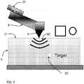
- FIG. 1 schematically shows an atomic force microscopy device, the device comprising a scan head 3 with a probe 2.
- the probe 2 embodiments of which are shown in FIG. 2,2A,2B,2C and FIG. 3, 3A comprises a flexible carrier such as a cantilever 8 (or a membrane) and a probe tip 9 arranged on the flexible carrier.
- the scan head 3 enables scanning of the probe 2 relative to the surface 51 of a sample 5.
- the probe tip 9 is brought in contact with the surface 51 of the sample 5.
- the probe tip 9 may be scanned across the surface of the sample 5 in contact mode (continuous contact between the probe tip 9 and the surface of the sample 5) or tapping mode (periodic contact between the probe tip 9 and the surface of the sample 5 during each cycle of a vibration applied to the cantilever 8).
- a laser unit (not shown) provides a laser beam 10 that impinges on the cantilever 8 and reflects towards an optical detector 20. Using the optical detector 20, vibrations in the cantilever 8 can be sensed due to small deflections of the reflected beam 10 under influence of such vibrations. This provides an output signal 26 for further analysis.
- An actuator (not shown) is provided that cooperates with at least one of the scan head 3 or a sample holder (not shown) for moving the probe tip 9 and the sample 5 relative to each other in one or more directions parallel to the surface 51of the sample for scanning of the surface with the probe tip.
- the laser unit and the optical detector 20 form a tip position detector for measuring motion of the probe tip relative to the scan head during said scanning, wherein the detector 20 provides the output signal 26 indicative for the motion.
- any suitable type of position detector may be applied, such as a piezo-resistive layer, the electrical resistance of which varies with probe deflection.
- Probe deflection may in that case be detected by detecting voltage differences in an electric signal applied to the piezo-resistive layer.
- probe deflection may be detected using a piezo-electric element or layer, the potential of which changes dependent on cantilever motion.
- capacitive measurements may be applied in an electrostatic sensing technique.
- one may also apply an interferometer to measure probe deflection or perform a heat flux measurement in a thermal method by using a temperature difference between probe and sample.
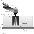
- the atomic force microscopy device comprises a first actuator 31 for applying a first acoustic input signal 92 comprising a signal component at a first frequency to at least one of the probe or the sample.
- the first acoustic input signal 92 is induced by an actuator 31, here a piezo electric actuator attached to the cantilever 8.
- the first actuator is a high frequency actuator 91, e.g. a piezo-electric actuator or an electrostatic actuator is mechanically coupled to the tip 9.
- An analysis system/controller 40 is provided for receiving and analyzing the output signal 26 from the tip position detector 20.
- a generator 6 provides a first input signal 61 and in addition thereto a second input signal 62.
- the first input signal 61 is periodic with a frequency fc
- the second input signal 62 is a periodic signal with a frequency fm.
- a mixer 63 modulates the first input signal 61 with the second input signal 62.
- Amplifier 64 amplifies the modulated signal so obtained and provides an amplified modulated signal 65 to the first actuator 31.
- FIG. 2 shows a side-view of a tip 9 in one embodiment of the device and FIG. 2A shows a cross-section according to IIA-IIA in FIG. 2.
- FIG. 2B and 2C respectively show of a tip 9 in other embodiments of the device according to the same cross-section.
- the tip is formed as a cone.
- the cone-shaped tip 9 has its largest cross-sectional area Amax at its base 95, where it is attached to the cantilever 8.
- the tip 9 tapers over a distance Dend towards its end.
- the square root R A of the largest cross-section Amax is equal to 150 nm and the distance Dend is equal to 100 nm.
- the tip is formed as a three-sided pyramid.
- the pyramid-shaped tip 9 has its largest cross-sectional area Amax at its base 95', where it is attached to the cantilever 8.
- the tip 9 tapers over a distance Dend towards its end.
- the square root RA of the largest cross-section Amax is equal to 120 nm and the distance Dend is equal to 100 nm.
- the tip is formed as a four-sided pyramid.
- the pyramid-shaped tip 9 has its largest cross-sectional area Amax at its base 95", where it is attached to the cantilever 8.
- the tip 9 tapers over a distance Dend towards its end.
- the square root RA of the largest cross-section Amax is equal to 200 nm and the distance Dend is equal to 150 nm.
- FIG. 3 shows a side-view of a tip 9 in another non-claimed embodiment of the device and FIG. 3A shows a cross-section according to IIIA-IIIA in FIG. 3 .
- the tip 9 has an extension portion 96 with which it is mounted onto the flexible carrier 8.
- the tip 9 includes a spherical body at the extension portion 96. From a central plane 95"", which has the largest cross-sectional area Amax the end portion tapers over a distance Dend equal to the radius of the sphere. In this case the ratio RA/Dend is equal to the square root of pi ( ⁇ ).
- RA may for example be 500 nm.
- FIG. 4 shows a side-view of a tip 9 in another non-claimed embodiment of the device and FIG. 4A shows a cross-section according to IVA-IVA in FIG. 4 .
- the tip 9 has an extension portion 96 with which it is mounted onto the flexible carrier 8.
- the tip has an end portion in the form of a truncated cone with its widest side at its end face 95′′′′′′ that faces away from the flexible carrier 8.
- the cross-section according to IVA-IVA in FIG. 4 coinciding with the end face 95′′′′′′ of the tip 9 has a cross-sectional area with a square root of 700 nm. As the cross-section coincides with the end face, the distance Dend between the end of the tip and the cross-section having the specified cross-sectional area is equal to 0, which complies with the requirement that it should be at most two times the value of said square root.
- the controller 40 is arranged for analyzing the output signal 26 for mapping at least subsurface nanostructures 52 below the surface 51 of the sample 5.
- Subsurface nanostructures 52 can be of various kinds, e.g. topological features formed by deliberately applied patterns in a layer or defects but may alternatively be non-topological features, such as density variations or stressed regions at a level below the surface 51 of the sample 5.
- the controller 40 may cooperate with additional modules as illustrated in FIG. 1 . In the embodiment shown these include a low-pass filter 41, a high pass filter 42 and a demodulator 43.
- the low-pass filter 41 selects a low frequent portion of the output signal 26, e.g.
- the high-pass filter 42 selects a high frequent portion Shf of the output signal 26, and provides this to the demodulator 43.
- the demodulator 43 demodulates this high frequent signal Shf using the modulation signal 62 to provide the demodulated signal Sdm.
- the demodulated signal Sdm at the output of demodulator 43 is indicative for subsurface features present in the sample 5.
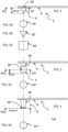
- FIG. 7 shows the amplitude of the demodulated signal Sdm as a function of the position x in a direction in a lateral direction with respect to the surface 51 of the sample 5.
- the signal to noise ratio of the signal is very low, which makes it impossible to locate such features.
- the signal to noise ratio in the signal resulting from a feature 52a is too much disturbed by measurement noise to be capable of identifying the feature. Larger features, e.g.
- feature 52b can still be detected in the signal Sdm, but due to their size, it is difficult to determine an accurate location indicative for their position. According to the present invention various approaches are offered for further processing to be applied to the demodulated signal Sdm in order to improve the spatial resolution.
- the demodulated signal is low-pass filtered by a low-pass filter 45 (See FIG. 1A ) to obtain a low-pass filtered feature signal S LP .
- a centroid detector 47 detects a centroid position in the low-pass filtered signal S LP and renders an output signal S centr indicative for a position x b of a detected sub-surface feature 52b determined on the basis of said centroid position in said low-pass filtered signal S LP .
- the low-pass filter 45 applied to the demodulated signal may for example be a box filter or another spatial filter such as a cosine or a Gaussian filter.
- the low-pass filter may have a spatial window in the same order of magnitude of the size s x of the features to be detected in the scanning direction x.
- the spatial window d w may have a size in the range of 0.2 s x to 5 s x . More preferably the spatial window d w may have a size in the range of 0.5 s x to 2 Sx.
- the size s x of the features that are detectable depends on various circumstances, such as the dimensions of the tip 9, the frequency range of the acoustic input signals and the depth of the features to be detected with respect to the sample surface 51.
- FIG. 1B Another approach is schematically illustrated in FIG. 1B .
- a marker position is estimated by curve fitting of an expected response curve to the demodulated signal S dm .
- a curve fitting module 48 is provided to perform this curve fitting on the demodulated signal S dm based on an input signal Ser specifying the expected response curve and to provide an output signal Smp indicative for the position of the marker estimated therewith.
- An optimal size s x to be selected for the features may be selected with the following procedure as illustrated in FIG. 8 .
- a test sample is provided at least substantially having the specifications corresponding to the device to be manufactured and provided with a set of subsurface features 521, 522, 523, 524 of mutually different size at a depth with respect to the surface where detection should take place.
- the wording "at least substantially having the specifications” implies that the device at least substantially has the same number of layers e.g. +/- 10% of the number of layers of the device to be manufactured and that the layers are manufactured of similar materials.
- the test sample is similar to the device to be manufactured apart from the set of subsurface features.
- the set of subsurface features may for example have a sizes selected from the range of 10 nm to 1 micron.
- a set of square shaped subsurface features may be provided subsequently having the sizes: 10 nm, 20 nm, 50 nm, 100 nm. 200 nm, 500 nm, 1000 nm.
- the test sample is scanned with the method according to the second aspect of the invention, while subsequently processing the demodulated signal S dm using subsequently different spatial window sizes d w each time corresponding to a respective size of the set of subsurface features. It is noted that it is sufficient to perform a single scan to obtain a demodulated signal S dm , and to subsequently process this demodulated signal Sdm using the subsequently different spatial window sizes d w .
- the position of each of the subsurface features 521, 522, 523 and 524 is estimated using the signal S LP1 , S LP2 , S LP3 , S LP4 , obtained with the low-pass filter having the corresponding window size d w1 , d w2 , d w3 , d w4 , Then a deviation ⁇ 1 , ⁇ 2 , ⁇ 3 , ⁇ 4 .
- the size the subsurface feature having the smallest absolute value for the deviation is selected as the size of the markers to be used in the manufacturing stage.
- FIG. 8 can analogically be used in combination with the detection method as described with reference to FIG. 1B .
- the expected response curve as indicated by the signal Ser is adapted to the specifications of the subsurface features 521, 522, 523 and 524.
- FIG. 9 schematically shows a lithographic system 100 for manufacturing of a multilayer semiconductor device 5.
- the lithographic system 100 comprises an atomic force microscopy device 110a according to the second aspect of the invention.
- the lithographic system is arranged to manufacture the semiconductor device in mutually subsequent manufacturing stages 100a, 100b, ..100n.
- the mutually subsequent manufacturing stages 100a, 100b, ..100n at least comprise a first manufacturing stage 100a and a second manufacturing stage 100b.
- the atomic force microscopy device 110a is arranged to inspect a semi-finished product 5' obtained in the first manufacturing stage 100a and to provide an analysis signal S align indicative for a position of sub-surface features in the semi-finished product 5'.
- the lithographic system 100 is arranged to use the analysis signal S align for alignment of the semi-finished product 5' in the second manufacturing stage 100b.
- the lithographic system 100 comprises a further atomic force microscopy device 110n that analyses a quality of the multilayer semiconductor device 5 and provides an output signal S Q indicative for said quality.
- the output signal S Q may be provided as a binary signal that indicates whether or not the quality of the semiconductor device meets predetermined requirements. Alternatively, or in addition the output signal SQ may provide diagnostic information enabling an operator of the lithographic system to improve its operation.
Landscapes
- Physics & Mathematics (AREA)
- General Physics & Mathematics (AREA)
- Health & Medical Sciences (AREA)
- General Health & Medical Sciences (AREA)
- Nuclear Medicine, Radiotherapy & Molecular Imaging (AREA)
- Radiology & Medical Imaging (AREA)
- Chemical & Material Sciences (AREA)
- Life Sciences & Earth Sciences (AREA)
- Acoustics & Sound (AREA)
- Analytical Chemistry (AREA)
- Biochemistry (AREA)
- Immunology (AREA)
- Pathology (AREA)
- Engineering & Computer Science (AREA)
- Power Engineering (AREA)
- Length Measuring Devices With Unspecified Measuring Means (AREA)
- Control Of Heat Treatment Processes (AREA)
- Investigating Or Analyzing Materials By The Use Of Ultrasonic Waves (AREA)
Claims (15)
- Dispositif de microscopie à force atomique (110a,...,110n), le dispositif comprenant une tête de balayage (3), la tête de balayage comprenant une sonde (2), la sonde comprenant un support flexible et une pointe de sonde (9) agencée sur le support flexible (8), dans lequel le dispositif de microscopie à force atomique est agencé pour déterminer des structures souterraines dans un échantillon (5), dans lequel le dispositif de microscopie à force atomique comprend en outre :un actionneur coopérant avec au moins l'un parmi la tête de balayage (3) ou un porte-substrat pour déplacer la pointe de sonde (9) et l'échantillon (5) l'un par rapport à l'autre dans une ou plusieurs directions parallèles à une surface (51) de l'échantillon pour balayer la surface avec la pointe de sonde ;un détecteur de position de pointe (20) pour mesurer un mouvement de la pointe de sonde par rapport à la tête de balayage pendant ledit balayage, le détecteur étant agencé pour fournir un signal de sortie (26) indicatif dudit mouvement ; etun dispositif de commande (40) pour recevoir et analyser le signal de sortie provenant du détecteur de position de pointe ;dans lequel le dispositif de microscopie à force atomique comprend en outre :un premier actionneur (31) pour appliquer un premier signal d'entrée acoustique comprenant une composante de signal (61) à une première fréquence à au moins l'un parmi la sonde ou l'échantillon ;dans lequel le dispositif de commande est agencé pour analyser le signal de sortie pour cartographier au moins des nanostructures souterraines (52) sous la surface (51) de l'échantillon (5), dans lequel la pointe de sonde (9) a une partie d'extrémité avec une extrémité faisant face à l'opposé dudit support flexible, dans lequel ladite partie d'extrémité a une coupe transversale la plus grande avec une surface en coupe transversale Acx, dont une racine carrée est d'au moins 100 nm et dans lequel une distance Dend entre ladite extrémité et ladite coupe transversale la plus grande est égale à au plus deux fois la valeur de ladite racine carrée, caractérisé en ce que ledit dispositif de commande comprend un premier module de traitement (43) pour reconstruire un signal caractéristique (Sdm) à partir dudit signal de sortie (Sscan), ledit signal caractéristique (Sdm) étant un signal démodulé (Sdm), un second module de traitement (45) pour un filtrage passe-bas dudit signal caractéristique et pour fournir un signal filtré passe-bas (SLP) et, selon une première option, comprenant en outre un module d'identification de centroïde (47) détectant une position de centroïde (Scentr) dans ledit signal filtré passe-bas SLP et restituant un signal de sortie (Scentr) indiquant la position de centroïde en tant que position d'une caractéristique souterraine détectée ou, selon une seconde option, comprenant en outre un module d'ajustement de courbe (48) pour effectuer un ajustement de courbe sur le signal démodulé (Sdm) sur la base d'un signal d'entrée (Ser) spécifiant une courbe de réponse attendue pour un marqueur présent en tant que structure souterraine dans l'échantillon, et pour fournir un signal de sortie (Smp) indicatif d'une position du marqueur estimé avec celui-ci.
- Dispositif de microscopie à force atomique selon la revendication 1, dans lequel la racine carrée de ladite coupe transversale la plus grande Amax est d'au moins 200 nm.
- Dispositif de microscopie à force atomique selon la revendication 2, dans lequel la racine carrée de ladite coupe transversale la plus grande Amax est d'au moins 500 nm.
- Dispositif de microscopie à force atomique selon l'une des revendications précédentes, dans lequel le premier actionneur est agencé pour appliquer le premier signal d'entrée acoustique à la sonde (2), dans lequel le premier actionneur comprend au moins un élément d'un groupe comprenant : un transducteur acoustique connecté à au moins l'un du support flexible (8) ou de la pointe de sonde (9), un actionneur électrostatique coopérant avec le support flexible, un actionneur électrostatique coopérant avec la pointe de sonde, la pointe de sonde étant fixée de manière flexible au support flexible, un actionneur piézoélectrique (31) coopérant avec le support flexible, un actionneur piézoélectrique (91) coopérant avec la pointe de sonde, la pointe de sonde étant fixée de manière flexible au support flexible, ou une source optique pulsée pour une excitation photothermique d'au moins l'un du support flexible ou de la pointe de sonde, telle qu'un laser pulsé.
- Dispositif de microscopie à force atomique selon l'une des revendications précédentes, comprenant en outre une source optique pulsée pour appliquer ledit premier signal d'entrée acoustique ou un autre signal d'entrée acoustique au moyen d'une excitation photothermique de la surface de l'échantillon.
- Procédé de détermination de structures souterraines (52, 521, 522, 523, 524) dans un échantillon à l'aide d'un système de microscopie à force atomique (100a,...,100n), dans lequel le système de microscopie à force atomique comprend au moins une tête de balayage (3), la tête de balayage comprenant une sonde (2), la sonde comprenant un support flexible (8) et une pointe de sonde (9) disposée sur le support flexible, dans lequel le procédé comprend :le déplacement de la pointe de sonde (9) et de l'échantillon (5) l'un par rapport à l'autre dans une ou plusieurs directions parallèles à une surface (51) de l'échantillon (5) pour balayer ladite surface avec la pointe de sonde ; etla surveillance du mouvement de la pointe de sonde (9) par rapport à la tête de balayage (3) avec un détecteur de position de pointe (20) pendant ledit balayage pour obtenir un signal de sortie (26) ;dans lequel le procédé comprend en outre :pendant ledit balayage, l'application d'au moins un premier signal d'entrée acoustique comprenant une composante de signal (61) à une première fréquence à au moins l'un parmi la sonde (2) ou l'échantillon (5) ;l'analyse du signal de sortie (26) pour cartographier au moins des nanostructures souterraines (52, 521, 522, 523, 524) sous la surface (51) de l'échantillon (5), dans lequel la pointe de sonde (9) a une partie d'extrémité avec une extrémité faisant face à l'opposé dudit support flexible (8), dans lequel ladite partie d'extrémité a une coupe transversale la plus grande avec une surface en coupe transversale Acx, dont une racine carrée est d'au moins 100 nm et dans lequel une distance Dend entre ladite extrémité et ladite coupe transversale la plus grande est égale à au plus deux fois la valeur de ladite racine carrée, caractérisé par la génération d'un signal démodulé (Sdm) à partir dudit signal de sortie (26), le filtrage passe-bas dudit signal démodulé pour obtenir un signal filtré passe-bas (SLP), et, selon une première option, la détection en outre d'une position de centroïde (Scentr) dans ledit signal filtré passe-bas (SLP) et la fourniture d'un signal de sortie (Scentr) indiquant la position de centroïde en tant que position d'une caractéristique souterraine détectée, ou, selon une seconde option, l'estimation en outre d'une position d'un marqueur, présent sous forme d'une caractéristique souterraine dans l'échantillon, par ajustement de courbe du signal démodulé (Sdm) sur la base d'une courbe de réponse attendue pour un marqueur, et par fourniture d'un signal de sortie (Smp) indicatif de la position du marqueur estimée avec celui-ci.
- Procédé selon la revendication 6 selon ladite première option, comprenant en outre la sélection d'une taille d'un marqueur et d'une taille de fenêtre pour le filtrage passe-bas dudit signal démodulé (Sdm), le procédé comprenant la fourniture d'un échantillon test avec un ensemble de caractéristiques souterraines (521, 522, 523, 524) ayant des tailles mutuellement différentes, l'utilisation du procédé pour déterminer le signal démodulé (Sdm), le filtrage passe-bas du signal démodulé avec un ensemble de filtres passe-bas ayant des tailles de fenêtre respectives correspondant aux tailles desdites caractéristiques souterraines dans ledit échantillon test, la détection d'une position de centroïde de chacune de l'ensemble de caractéristiques souterraines dans le signal filtré passe-bas obtenu avec le filtre passe-bas ayant la taille de fenêtre correspondante et l'estimation d'une position de la caractéristique souterraine détectée sur la base de la position de centroïde de chacune des caractéristiques souterraines dans son signal caractéristique filtré passe-bas correspondant.
- Procédé selon la revendication 6 ou 7, dans lequel l'échantillon (5) est un dispositif semi-conducteur multicouche semi-fini comprenant une couche de réserve recouvrant une ou plusieurs couches comprenant la au moins une première couche de dispositif, le procédé comprenant en outre les étapes consistant à- en tant que partie de l'analyse dudit signal de sortie, déterminer l'alignement des structures souterraines définies par le au moins un marqueur et/ou par un motif dans ladite au moins une première couche de dispositif,- adapter l'alignement du dispositif semi-conducteur par rapport à un alignement d'une autre couche de dispositif à motif à former sur le dispositif semi-conducteur multicouche semi-fini, sur la base de l'alignement déterminé desdites structures souterraines.
- Procédé selon la revendication 6 ou 7, dans lequel le dispositif (5) est un dispositif semi-conducteur qui comprend un empilement de couches de dispositif comprenant au moins une seconde couche de dispositif à motif en plus de ladite au moins une première couche de dispositif à motif, et le procédé comprenant en outre l'étape de détermination d'une erreur de superposition entre la au moins une première couche à motif et la au moins une seconde couche à motif sur la base de l'analyse.
- Procédé selon l'une des revendications 6 à 9, dans lequel le au moins un premier signal d'entrée acoustique (61) est appliqué en l'absence d'un autre signal d'entrée acoustique, et dans lequel la première fréquence est dans une plage de 0,01 mégahertz à 100 mégahertz.
- Procédé selon l'une des revendications 6 à 9, dans lequel le au moins un premier signal d'entrée acoustique (65) comprend diverses composantes de signal.
- Procédé selon l'une des revendications 6 à 9, dans lequel la première fréquence du au moins un premier signal acoustique d'entrée a une valeur d'au moins 1 GHz.
- Procédé selon la revendication 12, dans lequel ledit au moins un premier signal acoustique d'entrée est appliqué à la sonde (2), le au moins un premier signal acoustique comprenant en plus de ladite première composante une deuxième composante d'une seconde fréquence inférieure à ladite première fréquence, ladite première composante étant fournie d'une manière pulsée, et dans lequel ladite analyse comprend des mesures acoustiques d'écho.
- Procédé selon la revendication 13, dans lequel un second signal acoustique d'entrée est appliqué à l'échantillon, le second signal acoustique d'entrée comprenant au moins une troisième composante à une fréquence ayant une valeur dans la plage comprise entre la valeur de ladite seconde fréquence et de ladite première fréquence.
- Système lithographique (100) pour la fabrication d'un dispositif semi-conducteur multicouche (5), le système comprenant un dispositif de microscopie à force atomique (110a,..., 110n) selon l'une quelconque des revendications 1 à 5.
Applications Claiming Priority (2)
| Application Number | Priority Date | Filing Date | Title |
|---|---|---|---|
| EP17151418.5A EP3349018A1 (fr) | 2017-01-13 | 2017-01-13 | Dispositif de microscopie à force atomique, procédé et système lithographique |
| PCT/NL2018/050023 WO2018132007A1 (fr) | 2017-01-13 | 2018-01-12 | Système lithographique, procédé et dispositif de microscopie à force atomique |
Publications (2)
| Publication Number | Publication Date |
|---|---|
| EP3568703A1 EP3568703A1 (fr) | 2019-11-20 |
| EP3568703B1 true EP3568703B1 (fr) | 2023-03-01 |
Family
ID=57796253
Family Applications (2)
| Application Number | Title | Priority Date | Filing Date |
|---|---|---|---|
| EP17151418.5A Withdrawn EP3349018A1 (fr) | 2017-01-13 | 2017-01-13 | Dispositif de microscopie à force atomique, procédé et système lithographique |
| EP18702350.2A Active EP3568703B1 (fr) | 2017-01-13 | 2018-01-12 | Dispositif de microscopie à force atomique, procédé et système lithographique |
Family Applications Before (1)
| Application Number | Title | Priority Date | Filing Date |
|---|---|---|---|
| EP17151418.5A Withdrawn EP3349018A1 (fr) | 2017-01-13 | 2017-01-13 | Dispositif de microscopie à force atomique, procédé et système lithographique |
Country Status (5)
| Country | Link |
|---|---|
| US (1) | US10976345B2 (fr) |
| EP (2) | EP3349018A1 (fr) |
| KR (1) | KR102484672B1 (fr) |
| TW (1) | TWI787227B (fr) |
| WO (1) | WO2018132007A1 (fr) |
Families Citing this family (17)
| Publication number | Priority date | Publication date | Assignee | Title |
|---|---|---|---|---|
| EP3232192A1 (fr) * | 2016-04-14 | 2017-10-18 | Nederlandse Organisatie voor toegepast- natuurwetenschappelijk onderzoek TNO | Procédé de microscopie à sonde à balayage hétérodyne, système de microscopie à sonde à balayage et sonde correspondante |
| EP3690449A1 (fr) * | 2019-02-04 | 2020-08-05 | Nederlandse Organisatie voor toegepast- natuurwetenschappelijk onderzoek TNO | Cantilever, dispositif de microscopie acoustique ultrasonore comprenant le cantilever, son procédé d'utilisation et système lithographique le comprenant |
| NL2022516B1 (en) * | 2019-02-05 | 2020-09-08 | Nearfield Instr B V | Method of and arrangement for mapping structural features on a surface of a sample by scanning probe microscopy. |
| NL2025275B1 (en) * | 2020-04-03 | 2021-10-25 | Nearfield Instr B V | Method of determining dimensions of features of a subsurface topography, scanning probe microscopy system and computer program. |
| EP3901701A1 (fr) * | 2020-04-23 | 2021-10-27 | Nederlandse Organisatie voor toegepast- natuurwetenschappelijk Onderzoek TNO | Détermination de l'alignement de couches dans un produit stratifié |
| US12251991B2 (en) | 2020-08-20 | 2025-03-18 | Denso International America, Inc. | Humidity control for olfaction sensors |
| US11636870B2 (en) | 2020-08-20 | 2023-04-25 | Denso International America, Inc. | Smoking cessation systems and methods |
| US12377711B2 (en) | 2020-08-20 | 2025-08-05 | Denso International America, Inc. | Vehicle feature control systems and methods based on smoking |
| US11760169B2 (en) | 2020-08-20 | 2023-09-19 | Denso International America, Inc. | Particulate control systems and methods for olfaction sensors |
| US12017506B2 (en) | 2020-08-20 | 2024-06-25 | Denso International America, Inc. | Passenger cabin air control systems and methods |
| US11881093B2 (en) | 2020-08-20 | 2024-01-23 | Denso International America, Inc. | Systems and methods for identifying smoking in vehicles |
| US11813926B2 (en) | 2020-08-20 | 2023-11-14 | Denso International America, Inc. | Binding agent and olfaction sensor |
| US11760170B2 (en) | 2020-08-20 | 2023-09-19 | Denso International America, Inc. | Olfaction sensor preservation systems and methods |
| US11828210B2 (en) | 2020-08-20 | 2023-11-28 | Denso International America, Inc. | Diagnostic systems and methods of vehicles using olfaction |
| US12269315B2 (en) | 2020-08-20 | 2025-04-08 | Denso International America, Inc. | Systems and methods for measuring and managing odor brought into rental vehicles |
| US11932080B2 (en) | 2020-08-20 | 2024-03-19 | Denso International America, Inc. | Diagnostic and recirculation control systems and methods |
| EP4050345B1 (fr) | 2021-02-26 | 2025-02-26 | Materials Center Leoben Forschung GmbH | Sonde de mesure permettant d'examiner des zones de surface |
Family Cites Families (7)
| Publication number | Priority date | Publication date | Assignee | Title |
|---|---|---|---|---|
| FR2697087B1 (fr) * | 1992-10-19 | 1995-01-06 | Centre Nat Rech Scient | Procédé acoustique d'analyse microscopique ou d'imagerie d'un objet en profondeur par application d'une pointe vibrante et microscope en faisant application. |
| JPH08254542A (ja) * | 1995-01-09 | 1996-10-01 | Texas Instr Inc <Ti> | ナノメートルスケールで試料を同定し特性を確定するための方法および装置 |
| US6392229B1 (en) * | 1999-01-12 | 2002-05-21 | Applied Materials, Inc. | AFM-based lithography metrology tool |
| JP4746104B2 (ja) * | 2005-10-06 | 2011-08-10 | ノースウエスタン ユニバーシティ | 走査型近視野超音波ホログラフィー |
| CN101029862B (zh) * | 2007-03-19 | 2010-10-20 | 中国科学院上海硅酸盐研究所 | 基于原子力显微镜的声成像用弱信号检测器 |
| EP2150973B1 (fr) * | 2007-05-10 | 2020-05-06 | Bruker Nano, Inc. | Microscopie ultrasonore non destructive de sous-surface a l'echelle d'une tranche, utilisant une detection afm de champ proche |
| EP2940480A1 (fr) * | 2014-04-28 | 2015-11-04 | Nederlandse Organisatie voor toegepast- natuurwetenschappelijk onderzoek TNO | Procédé permettant de faire avancer une pointe de sonde d'un dispositif de microscopie à balayage vers une surface d'échantillon et dispositif à cet effet |
-
2017
- 2017-01-13 EP EP17151418.5A patent/EP3349018A1/fr not_active Withdrawn
-
2018
- 2018-01-12 EP EP18702350.2A patent/EP3568703B1/fr active Active
- 2018-01-12 KR KR1020197022732A patent/KR102484672B1/ko active Active
- 2018-01-12 WO PCT/NL2018/050023 patent/WO2018132007A1/fr not_active Ceased
- 2018-01-12 US US16/477,820 patent/US10976345B2/en active Active
- 2018-01-15 TW TW107101423A patent/TWI787227B/zh active
Also Published As
| Publication number | Publication date |
|---|---|
| US20190369139A1 (en) | 2019-12-05 |
| US10976345B2 (en) | 2021-04-13 |
| EP3349018A1 (fr) | 2018-07-18 |
| KR102484672B1 (ko) | 2023-01-04 |
| WO2018132007A1 (fr) | 2018-07-19 |
| TW201831906A (zh) | 2018-09-01 |
| EP3568703A1 (fr) | 2019-11-20 |
| KR20190107687A (ko) | 2019-09-20 |
| TWI787227B (zh) | 2022-12-21 |
Similar Documents
| Publication | Publication Date | Title |
|---|---|---|
| US10976345B2 (en) | Atomic force microscopy device, method and lithographic system | |
| US7798001B2 (en) | Scanning near field ultrasound holography | |
| Stan et al. | Mapping the elastic properties of granular Au films by contact resonance atomic force microscopy | |
| TWI766932B (zh) | 外差式原子力顯微術裝置、方法以及微影製程系統 | |
| EP3443363B1 (fr) | Procédé de réglages de paramètres de syntonisation pour effectuer une microscopie à sonde de balayage acoustique pour imagerie souterraine, système de microscopie à sonde à balayage, et produit de programme informatique | |
| KR102405671B1 (ko) | 반도체 소자 또는 반가공 반도체 소자의 레이어의 결함 탐지 또는 특성화를 수행하는 방법 및 시스템 | |
| WO2018132008A1 (fr) | Procédé et système pour la détection de structures se trouvant sur ou sous la surface d'un échantillon à l'aide d'une sonde comprenant un porte-à-faux et une pointe de sonde | |
| EP1952204A1 (fr) | Holographie ultrasonore de champ proche a balayage | |
| EP3646117B1 (fr) | Procédé, système de microscopie à force atomique et produit-programme d'ordinateur | |
| EP3507607B1 (fr) | Procédé pour mesurer les dommages sur un substrat provoqués par un faisceau d'électrons | |
| CN101303221A (zh) | 基于原子力显微镜的纳米结构中纳米间隙的精密测量方法 |
Legal Events
| Date | Code | Title | Description |
|---|---|---|---|
| STAA | Information on the status of an ep patent application or granted ep patent |
Free format text: STATUS: UNKNOWN |
|
| STAA | Information on the status of an ep patent application or granted ep patent |
Free format text: STATUS: THE INTERNATIONAL PUBLICATION HAS BEEN MADE |
|
| PUAI | Public reference made under article 153(3) epc to a published international application that has entered the european phase |
Free format text: ORIGINAL CODE: 0009012 |
|
| STAA | Information on the status of an ep patent application or granted ep patent |
Free format text: STATUS: REQUEST FOR EXAMINATION WAS MADE |
|
| 17P | Request for examination filed |
Effective date: 20190805 |
|
| AK | Designated contracting states |
Kind code of ref document: A1 Designated state(s): AL AT BE BG CH CY CZ DE DK EE ES FI FR GB GR HR HU IE IS IT LI LT LU LV MC MK MT NL NO PL PT RO RS SE SI SK SM TR |
|
| AX | Request for extension of the european patent |
Extension state: BA ME |
|
| DAV | Request for validation of the european patent (deleted) | ||
| DAX | Request for extension of the european patent (deleted) | ||
| STAA | Information on the status of an ep patent application or granted ep patent |
Free format text: STATUS: EXAMINATION IS IN PROGRESS |
|
| 17Q | First examination report despatched |
Effective date: 20210630 |
|
| GRAP | Despatch of communication of intention to grant a patent |
Free format text: ORIGINAL CODE: EPIDOSNIGR1 |
|
| STAA | Information on the status of an ep patent application or granted ep patent |
Free format text: STATUS: GRANT OF PATENT IS INTENDED |
|
| INTG | Intention to grant announced |
Effective date: 20220907 |
|
| GRAS | Grant fee paid |
Free format text: ORIGINAL CODE: EPIDOSNIGR3 |
|
| GRAA | (expected) grant |
Free format text: ORIGINAL CODE: 0009210 |
|
| STAA | Information on the status of an ep patent application or granted ep patent |
Free format text: STATUS: THE PATENT HAS BEEN GRANTED |
|
| AK | Designated contracting states |
Kind code of ref document: B1 Designated state(s): AL AT BE BG CH CY CZ DE DK EE ES FI FR GB GR HR HU IE IS IT LI LT LU LV MC MK MT NL NO PL PT RO RS SE SI SK SM TR |
|
| REG | Reference to a national code |
Ref country code: GB Ref legal event code: FG4D |
|
| REG | Reference to a national code |
Ref country code: CH Ref legal event code: EP Ref country code: AT Ref legal event code: REF Ref document number: 1551333 Country of ref document: AT Kind code of ref document: T Effective date: 20230315 |
|
| REG | Reference to a national code |
Ref country code: DE Ref legal event code: R096 Ref document number: 602018046633 Country of ref document: DE |
|
| REG | Reference to a national code |
Ref country code: IE Ref legal event code: FG4D |
|
| REG | Reference to a national code |
Ref country code: NL Ref legal event code: FP |
|
| REG | Reference to a national code |
Ref country code: LT Ref legal event code: MG9D |
|
| P01 | Opt-out of the competence of the unified patent court (upc) registered |
Effective date: 20230522 |
|
| PG25 | Lapsed in a contracting state [announced via postgrant information from national office to epo] |
Ref country code: RS Free format text: LAPSE BECAUSE OF FAILURE TO SUBMIT A TRANSLATION OF THE DESCRIPTION OR TO PAY THE FEE WITHIN THE PRESCRIBED TIME-LIMIT Effective date: 20230301 Ref country code: NO Free format text: LAPSE BECAUSE OF FAILURE TO SUBMIT A TRANSLATION OF THE DESCRIPTION OR TO PAY THE FEE WITHIN THE PRESCRIBED TIME-LIMIT Effective date: 20230601 Ref country code: LV Free format text: LAPSE BECAUSE OF FAILURE TO SUBMIT A TRANSLATION OF THE DESCRIPTION OR TO PAY THE FEE WITHIN THE PRESCRIBED TIME-LIMIT Effective date: 20230301 Ref country code: LT Free format text: LAPSE BECAUSE OF FAILURE TO SUBMIT A TRANSLATION OF THE DESCRIPTION OR TO PAY THE FEE WITHIN THE PRESCRIBED TIME-LIMIT Effective date: 20230301 Ref country code: HR Free format text: LAPSE BECAUSE OF FAILURE TO SUBMIT A TRANSLATION OF THE DESCRIPTION OR TO PAY THE FEE WITHIN THE PRESCRIBED TIME-LIMIT Effective date: 20230301 Ref country code: ES Free format text: LAPSE BECAUSE OF FAILURE TO SUBMIT A TRANSLATION OF THE DESCRIPTION OR TO PAY THE FEE WITHIN THE PRESCRIBED TIME-LIMIT Effective date: 20230301 |
|
| REG | Reference to a national code |
Ref country code: AT Ref legal event code: MK05 Ref document number: 1551333 Country of ref document: AT Kind code of ref document: T Effective date: 20230301 |
|
| PG25 | Lapsed in a contracting state [announced via postgrant information from national office to epo] |
Ref country code: SE Free format text: LAPSE BECAUSE OF FAILURE TO SUBMIT A TRANSLATION OF THE DESCRIPTION OR TO PAY THE FEE WITHIN THE PRESCRIBED TIME-LIMIT Effective date: 20230301 Ref country code: PL Free format text: LAPSE BECAUSE OF FAILURE TO SUBMIT A TRANSLATION OF THE DESCRIPTION OR TO PAY THE FEE WITHIN THE PRESCRIBED TIME-LIMIT Effective date: 20230301 Ref country code: GR Free format text: LAPSE BECAUSE OF FAILURE TO SUBMIT A TRANSLATION OF THE DESCRIPTION OR TO PAY THE FEE WITHIN THE PRESCRIBED TIME-LIMIT Effective date: 20230602 Ref country code: FI Free format text: LAPSE BECAUSE OF FAILURE TO SUBMIT A TRANSLATION OF THE DESCRIPTION OR TO PAY THE FEE WITHIN THE PRESCRIBED TIME-LIMIT Effective date: 20230301 |
|
| PG25 | Lapsed in a contracting state [announced via postgrant information from national office to epo] |
Ref country code: SM Free format text: LAPSE BECAUSE OF FAILURE TO SUBMIT A TRANSLATION OF THE DESCRIPTION OR TO PAY THE FEE WITHIN THE PRESCRIBED TIME-LIMIT Effective date: 20230301 Ref country code: RO Free format text: LAPSE BECAUSE OF FAILURE TO SUBMIT A TRANSLATION OF THE DESCRIPTION OR TO PAY THE FEE WITHIN THE PRESCRIBED TIME-LIMIT Effective date: 20230301 Ref country code: PT Free format text: LAPSE BECAUSE OF FAILURE TO SUBMIT A TRANSLATION OF THE DESCRIPTION OR TO PAY THE FEE WITHIN THE PRESCRIBED TIME-LIMIT Effective date: 20230703 Ref country code: EE Free format text: LAPSE BECAUSE OF FAILURE TO SUBMIT A TRANSLATION OF THE DESCRIPTION OR TO PAY THE FEE WITHIN THE PRESCRIBED TIME-LIMIT Effective date: 20230301 Ref country code: CZ Free format text: LAPSE BECAUSE OF FAILURE TO SUBMIT A TRANSLATION OF THE DESCRIPTION OR TO PAY THE FEE WITHIN THE PRESCRIBED TIME-LIMIT Effective date: 20230301 Ref country code: AT Free format text: LAPSE BECAUSE OF FAILURE TO SUBMIT A TRANSLATION OF THE DESCRIPTION OR TO PAY THE FEE WITHIN THE PRESCRIBED TIME-LIMIT Effective date: 20230301 |
|
| PG25 | Lapsed in a contracting state [announced via postgrant information from national office to epo] |
Ref country code: SK Free format text: LAPSE BECAUSE OF FAILURE TO SUBMIT A TRANSLATION OF THE DESCRIPTION OR TO PAY THE FEE WITHIN THE PRESCRIBED TIME-LIMIT Effective date: 20230301 Ref country code: IS Free format text: LAPSE BECAUSE OF FAILURE TO SUBMIT A TRANSLATION OF THE DESCRIPTION OR TO PAY THE FEE WITHIN THE PRESCRIBED TIME-LIMIT Effective date: 20230701 |
|
| REG | Reference to a national code |
Ref country code: DE Ref legal event code: R097 Ref document number: 602018046633 Country of ref document: DE |
|
| PLBE | No opposition filed within time limit |
Free format text: ORIGINAL CODE: 0009261 |
|
| STAA | Information on the status of an ep patent application or granted ep patent |
Free format text: STATUS: NO OPPOSITION FILED WITHIN TIME LIMIT |
|
| PG25 | Lapsed in a contracting state [announced via postgrant information from national office to epo] |
Ref country code: SI Free format text: LAPSE BECAUSE OF FAILURE TO SUBMIT A TRANSLATION OF THE DESCRIPTION OR TO PAY THE FEE WITHIN THE PRESCRIBED TIME-LIMIT Effective date: 20230301 Ref country code: DK Free format text: LAPSE BECAUSE OF FAILURE TO SUBMIT A TRANSLATION OF THE DESCRIPTION OR TO PAY THE FEE WITHIN THE PRESCRIBED TIME-LIMIT Effective date: 20230301 |
|
| 26N | No opposition filed |
Effective date: 20231204 |
|
| PG25 | Lapsed in a contracting state [announced via postgrant information from national office to epo] |
Ref country code: IT Free format text: LAPSE BECAUSE OF FAILURE TO SUBMIT A TRANSLATION OF THE DESCRIPTION OR TO PAY THE FEE WITHIN THE PRESCRIBED TIME-LIMIT Effective date: 20230301 |
|
| PG25 | Lapsed in a contracting state [announced via postgrant information from national office to epo] |
Ref country code: MC Free format text: LAPSE BECAUSE OF FAILURE TO SUBMIT A TRANSLATION OF THE DESCRIPTION OR TO PAY THE FEE WITHIN THE PRESCRIBED TIME-LIMIT Effective date: 20230301 |
|
| PG25 | Lapsed in a contracting state [announced via postgrant information from national office to epo] |
Ref country code: MC Free format text: LAPSE BECAUSE OF FAILURE TO SUBMIT A TRANSLATION OF THE DESCRIPTION OR TO PAY THE FEE WITHIN THE PRESCRIBED TIME-LIMIT Effective date: 20230301 |
|
| REG | Reference to a national code |
Ref country code: CH Ref legal event code: PL |
|
| PG25 | Lapsed in a contracting state [announced via postgrant information from national office to epo] |
Ref country code: LU Free format text: LAPSE BECAUSE OF NON-PAYMENT OF DUE FEES Effective date: 20240112 |
|
| GBPC | Gb: european patent ceased through non-payment of renewal fee |
Effective date: 20240112 |
|
| PG25 | Lapsed in a contracting state [announced via postgrant information from national office to epo] |
Ref country code: LU Free format text: LAPSE BECAUSE OF NON-PAYMENT OF DUE FEES Effective date: 20240112 |
|
| PG25 | Lapsed in a contracting state [announced via postgrant information from national office to epo] |
Ref country code: GB Free format text: LAPSE BECAUSE OF NON-PAYMENT OF DUE FEES Effective date: 20240112 |
|
| PG25 | Lapsed in a contracting state [announced via postgrant information from national office to epo] |
Ref country code: BE Free format text: LAPSE BECAUSE OF NON-PAYMENT OF DUE FEES Effective date: 20240131 |
|
| PG25 | Lapsed in a contracting state [announced via postgrant information from national office to epo] |
Ref country code: CH Free format text: LAPSE BECAUSE OF NON-PAYMENT OF DUE FEES Effective date: 20240131 |
|
| PG25 | Lapsed in a contracting state [announced via postgrant information from national office to epo] |
Ref country code: GB Free format text: LAPSE BECAUSE OF NON-PAYMENT OF DUE FEES Effective date: 20240112 Ref country code: CH Free format text: LAPSE BECAUSE OF NON-PAYMENT OF DUE FEES Effective date: 20240131 Ref country code: BE Free format text: LAPSE BECAUSE OF NON-PAYMENT OF DUE FEES Effective date: 20240131 |
|
| REG | Reference to a national code |
Ref country code: BE Ref legal event code: MM Effective date: 20240131 |
|
| PG25 | Lapsed in a contracting state [announced via postgrant information from national office to epo] |
Ref country code: BG Free format text: LAPSE BECAUSE OF FAILURE TO SUBMIT A TRANSLATION OF THE DESCRIPTION OR TO PAY THE FEE WITHIN THE PRESCRIBED TIME-LIMIT Effective date: 20230301 |
|
| PG25 | Lapsed in a contracting state [announced via postgrant information from national office to epo] |
Ref country code: BG Free format text: LAPSE BECAUSE OF FAILURE TO SUBMIT A TRANSLATION OF THE DESCRIPTION OR TO PAY THE FEE WITHIN THE PRESCRIBED TIME-LIMIT Effective date: 20230301 |
|
| PG25 | Lapsed in a contracting state [announced via postgrant information from national office to epo] |
Ref country code: CY Free format text: LAPSE BECAUSE OF FAILURE TO SUBMIT A TRANSLATION OF THE DESCRIPTION OR TO PAY THE FEE WITHIN THE PRESCRIBED TIME-LIMIT; INVALID AB INITIO Effective date: 20180112 |
|
| PG25 | Lapsed in a contracting state [announced via postgrant information from national office to epo] |
Ref country code: HU Free format text: LAPSE BECAUSE OF FAILURE TO SUBMIT A TRANSLATION OF THE DESCRIPTION OR TO PAY THE FEE WITHIN THE PRESCRIBED TIME-LIMIT; INVALID AB INITIO Effective date: 20180112 |
|
| PG25 | Lapsed in a contracting state [announced via postgrant information from national office to epo] |
Ref country code: TR Free format text: LAPSE BECAUSE OF FAILURE TO SUBMIT A TRANSLATION OF THE DESCRIPTION OR TO PAY THE FEE WITHIN THE PRESCRIBED TIME-LIMIT Effective date: 20230301 |
|
| PGFP | Annual fee paid to national office [announced via postgrant information from national office to epo] |
Ref country code: NL Payment date: 20260121 Year of fee payment: 9 |
|
| PGFP | Annual fee paid to national office [announced via postgrant information from national office to epo] |
Ref country code: DE Payment date: 20260121 Year of fee payment: 9 Ref country code: IE Payment date: 20260122 Year of fee payment: 9 |
|
| PGFP | Annual fee paid to national office [announced via postgrant information from national office to epo] |
Ref country code: FR Payment date: 20260123 Year of fee payment: 9 |